Nanophotonic lithium niobate electro-optic modulators · 2 a b Our Etched waveguide Traditional ion...
6
Nanophotonic lithium niobate electro-optic modulators Cheng Wang*, 1 Mian Zhang*, 1 Brian Stern, 2, 3 Michal Lipson, 3 and Marko Loncar 1 1 John A. Paulson School of Engineering and Applied Sciences, Harvard University, Cambridge, Massachusetts 02138, USA 2 School of Electrical and Computer Engineering, Cornell University, Ithaca, New York 14853, USA. 3 Department of Electrical Engineering, Columbia University, New York, New York 10027,USA (Dated: December 30, 2016) Modern communication networks require high performance and scalable electro-optic modulators that convert electrical signals to optical signals at high speed. Existing lithium niobate modula- tors have excellent performance but are bulky and prohibitively expensive to scale up. Here we demonstrate scalable and high-performance nanophotonic electro-optic modulators made of single- crystalline lithium niobate microring resonators and micro-Mach-Zehnder interferometers. We show a half-wave electro-optic modulation efficiency of 1.8V·cm and data rates up to 40 Gbps. Data centers, metropolitan and long-haul data commu- nication networks demand scalable and high-performance electro-optic modulators to convert electrical signals to modulated light waves at high speed [1, 2]. For decades, lithium niobate (LiNbO 3 , LN) has been the material of choice owing to its excellent properties - namely large electro-optic response, high intrinsic bandwidth, wide transparency window, exceptional signal quality and good temperature stability [1–3]. Existing LN modu- lators however are not scalable due to the difficulty in nanostructuring LN [2]. As a result, they remain bulky (∼ 10 cm long), discrete, expensive, and require high- power electrical drivers [1, 2]. Integrated silicon (Si) [4–7] and indium phosphide (InP) [8–10] photonics are promising solutions for scalability but come at the cost of compromised performance [4–10]. Here we demon- strate monolithically integrated LN electro-optic modu- lators that are orders of magnitudes smaller and more efficient than traditional bulk LN devices while preserv- ing LN’s excellent material properties. Our compact LN platform consists of low-loss nanoscale LN waveguides, micro-ring resonators and miniaturized Mach-Zehnder interferometers (MZI), fabricated by directly shaping LN thin films into sub-wavelength structures. To address the need of scalable and high-performance electro-optic modulators for modern data communica- tions, tremendous efforts have been made in recent years towards a variety of platforms that feature small foot- prints and high data bandwidths, including Si [4–7], InP [8–10], AlN [11], plasmonics [12], graphene [13–15] and polymers [16, 17]. However, these approaches have fundamental material limitations that are hard to over- come. For example, both Si and InP modulators rely on switching mechanisms (carrier injection and quantum- confinement Stark effect respectively) that are intrinsi- cally nonlinear, absorptive, and sensitive to temperature *These authors contributed equally to this work fluctuation [4–10]. Limitations of the other platforms in- clude low switching efficiency (AlN) [11], high optical loss (plasmonics) [12], challenging scalability (graphene) [15] and poor long term stability (polymer) [17]. LN remains the material of choice for high-performance electro-optic modulators due to its wide bandgap (high transparency) and large second order (χ 2 ) electro-optic coefficient (30 pm/V). In contrast to Si and InP, the χ 2 process in LN changes its index of refraction linearly with an applied electrical field, at femtosecond timescale. The efficiency of this process is determined by the overlap of the optical and the electrical fields. Conventional ion- diffused LN waveguides suffer from the low refractive index contrast (Δn< 0.02) between core and cladding (Fig. 1a), resulting in large optical modal volumes and bending radii [18]. As a result, the photonic structures are large and the radio-frequency (RF) electrodes have to be placed far away from the optical mode to prevent detrimental waveguide propagation loss, significantly re- ducing the electro-optic switching efficiency [1, 2]. Thin-film LN on insulator has recently emerged as a promising candidate to shrink the optical modal volume and boost the electro-optic efficiency [19]. While progress has been made towards chip-scale LN devices [19–29], realization of a monolithic LN nanophotonic circuit re- mains challenging due to the difficulty in LN dry etching. Instead, heterogeneous integration of intact LN thin films with another easy-to-etch material has been pursued [21– 24]. These hybrid platforms, however, suffer from low bandwidth performance and/or low optical confinement due to the addition of non-ideal deposited materials. For example, the hybrid Si/LN modulator has a bandwidth of ∼ 5 GHz due to the large resistance of the bonded silicon layer [21]. Ridge waveguides formed by depositing pas- sive index-matching materials (e.g. silicon nitride and chalcogenide) results in weakly confined optical modes and large bending (> 0.2 mm) [22–24].Furthermore, the electro-optic efficiencies in these heterogeneous devices
Transcript of Nanophotonic lithium niobate electro-optic modulators · 2 a b Our Etched waveguide Traditional ion...
Nanophotonic lithium niobate electro-optic modulators
Cheng Wang*,1 Mian Zhang*,1 Brian Stern,2, 3 Michal Lipson,3 and Marko Loncar1
1John A. Paulson School of Engineering and Applied Sciences,Harvard University, Cambridge, Massachusetts 02138, USA
2School of Electrical and Computer Engineering,Cornell University, Ithaca, New York 14853, USA.
3Department of Electrical Engineering, Columbia University, New York, New York 10027,USA(Dated: December 30, 2016)
Modern communication networks require high performance and scalable electro-optic modulatorsthat convert electrical signals to optical signals at high speed. Existing lithium niobate modula-tors have excellent performance but are bulky and prohibitively expensive to scale up. Here wedemonstrate scalable and high-performance nanophotonic electro-optic modulators made of single-crystalline lithium niobate microring resonators and micro-Mach-Zehnder interferometers. We showa half-wave electro-optic modulation efficiency of 1.8V·cm and data rates up to 40 Gbps.
Data centers, metropolitan and long-haul data commu-nication networks demand scalable and high-performanceelectro-optic modulators to convert electrical signals tomodulated light waves at high speed [1, 2]. For decades,lithium niobate (LiNbO3, LN) has been the material ofchoice owing to its excellent properties - namely largeelectro-optic response, high intrinsic bandwidth, widetransparency window, exceptional signal quality andgood temperature stability [1–3]. Existing LN modu-lators however are not scalable due to the difficulty innanostructuring LN [2]. As a result, they remain bulky(∼ 10 cm long), discrete, expensive, and require high-power electrical drivers [1, 2]. Integrated silicon (Si)[4–7] and indium phosphide (InP) [8–10] photonics arepromising solutions for scalability but come at the costof compromised performance [4–10]. Here we demon-strate monolithically integrated LN electro-optic modu-lators that are orders of magnitudes smaller and moreefficient than traditional bulk LN devices while preserv-ing LN’s excellent material properties. Our compact LNplatform consists of low-loss nanoscale LN waveguides,micro-ring resonators and miniaturized Mach-Zehnderinterferometers (MZI), fabricated by directly shaping LNthin films into sub-wavelength structures.
To address the need of scalable and high-performanceelectro-optic modulators for modern data communica-tions, tremendous efforts have been made in recent yearstowards a variety of platforms that feature small foot-prints and high data bandwidths, including Si [4–7],InP [8–10], AlN [11], plasmonics [12], graphene [13–15]and polymers [16, 17]. However, these approaches havefundamental material limitations that are hard to over-come. For example, both Si and InP modulators rely onswitching mechanisms (carrier injection and quantum-confinement Stark effect respectively) that are intrinsi-cally nonlinear, absorptive, and sensitive to temperature
*These authors contributed equally to this work
fluctuation [4–10]. Limitations of the other platforms in-clude low switching efficiency (AlN) [11], high optical loss(plasmonics) [12], challenging scalability (graphene) [15]and poor long term stability (polymer) [17].
LN remains the material of choice for high-performanceelectro-optic modulators due to its wide bandgap (hightransparency) and large second order (χ2) electro-opticcoefficient (30 pm/V). In contrast to Si and InP, the χ2
process in LN changes its index of refraction linearly withan applied electrical field, at femtosecond timescale. Theefficiency of this process is determined by the overlap ofthe optical and the electrical fields. Conventional ion-diffused LN waveguides suffer from the low refractiveindex contrast (∆n < 0.02) between core and cladding(Fig. 1a), resulting in large optical modal volumes andbending radii [18]. As a result, the photonic structuresare large and the radio-frequency (RF) electrodes haveto be placed far away from the optical mode to preventdetrimental waveguide propagation loss, significantly re-ducing the electro-optic switching efficiency [1, 2].
Thin-film LN on insulator has recently emerged as apromising candidate to shrink the optical modal volumeand boost the electro-optic efficiency [19]. While progresshas been made towards chip-scale LN devices [19–29],realization of a monolithic LN nanophotonic circuit re-mains challenging due to the difficulty in LN dry etching.Instead, heterogeneous integration of intact LN thin filmswith another easy-to-etch material has been pursued [21–24]. These hybrid platforms, however, suffer from lowbandwidth performance and/or low optical confinementdue to the addition of non-ideal deposited materials. Forexample, the hybrid Si/LN modulator has a bandwidth of∼ 5 GHz due to the large resistance of the bonded siliconlayer [21]. Ridge waveguides formed by depositing pas-sive index-matching materials (e.g. silicon nitride andchalcogenide) results in weakly confined optical modesand large bending (> 0.2 mm) [22–24].Furthermore, theelectro-optic efficiencies in these heterogeneous devices

2
ba
Our Etchedwaveguide
Traditional ion diffusedwaveguide
LNAu
SiO2
FIG. 1. Device design. a. Schematics of a traditional ion-diffused LN waveguide (left) and our etched LN waveguide embeddedin SiO2 (right), roughly to scale. The light blue region indicates the approximate waveguiding core in each circumstance. Thelarger index contrast in etched waveguides allows for much stronger light confinement. b. Schematic view of the device layoutwith thin film LN waveguides and RF electrodes. Metal vias and bridges are fabricated to achieve modulation on both sides ofthe devices. Inset shows a schematic of the device cross-section with an overview of the metal bridge.
a
bd
c
z
x
Mach-Zehnder
RingRacetrack
h
s
g
w
100 μm
100 μm 1 μm
500 nm
FIG. 2. Fabricated optical devices and electrical contacts a-b. False-color scanning electron microscope (SEM) imagesof the fabricated racetrack and ring resonator based modulators (a) and Mach-Zehnder interferometer based modulators (b).c. Cross-section view of the simulated optical TE mode profile (Ez component) and RF electrical field (shown by arrows).The x-cut LN used here is most sensitive to the horizontal component of the electric field (Ez). h: LN waveguide height; w:waveguide width; s: LN slab thickness. g: metal electrode gap. d. Close-up SEM image of the metal electrodes and the opticalwaveguide.

3
1.0
0.8
0.6
0.4
0.2
Nor
mal
ized
Tra
nsm
issi
on
1576.11576.01575.91575.8
Wavelength (nm)
100
80
60
40
20Res
onan
ce s
hift
(pm
)
14121086420
DC offset (V)
ca b
-8 -6 -4 -2 0 2 4 6 8
DC offset (V)
0
0.2
0.4
0.6
0.8
1.0
+3V steps
FIG. 3. DC electrical and optical characterization a. Measured transmission spectra of a high Q (∼ 50,000) racetrackresonator exhibits large frequency shift with applied DC voltages. b. Linear resonant wavelength shift as a function of DCvoltage with error bars. The measured tuning efficiency is 7.0 pm/V. c. Optical transmission of a 2 mm long MZI modulatorversus DC voltage applied, indicating a half-wave voltage (Vπ) of 9 V and a voltage-length product of 1.8 V·cm.
are also compromised due to the reduced overlap betweenthe electric field and the active material region [21–24].
We demonstrate single-crystalline LN photonic struc-tures with submicron optical confinement, small bendingradii (< 20 µm) and low propagation loss by directlyshaping single-crystalline LN into nanoscale waveguides(Fig. 1a). The waveguides are defined on thin-film LN-on-insulator substrates using electron beam lithographyand subsequently dry etched in Ar+ plasma using a de-posited Si hard mask (Methods and Supplementary Fig.S1). The index contrast between the LN core and the sili-con dioxide (SiO2) cladding is ∆n = 0.67, over an order ofmagnitude higher than ion-diffused LN waveguides. Fig-ures 2a and 2b show a range of fabricated nanophotonicLN devices including nano-waveguides, ring resonators,racetrack resonators and MZIs. The typical propagationloss of these structures is ∼ 3 dB/cm, which is limitedby etching roughness [27] and can be further improvedby at least an order of magnitude [25, 30]. The resultingMZI and racetrack structures have low on-chip insertionloss of ∼ 2 dB and ∼ 1 dB respectively (with additional∼ 5 dB/facet coupling loss).
The highly confined optical mode allows us to maxi-mize electro-optic modulation efficiency by placing goldmicro-RF electrodes close to the LN waveguide (Figs. 2cand 2d). Our devices make use of an x-cut LN configu-ration, where transverse-electric (TE) optical modes andin-plane electric fields (Ez) interact through the highestelectro-optic tensor component (r33) of LN. We designthe waveguide geometry and the micro-RF electrode po-sitions to achieve the optimal overlap between the opticaland electric fields, while minimizing the bending loss andthe metal-induced absorption loss. Figure 2c shows thenumerically simulated overlap between the correspond-ing optical and electric fields. The optical waveguideshave a top width w = 900 nm, rib height h = 400 nm,
and a slab thickness s = 300 nm (Fig. 2c). To maximizethe in-plane electric field (Ez), we sandwich the opticalwaveguide between the signal and ground electrodes witha gap of g = 3.5 µm. A SiO2 cladding layer is used tofurther enhance this overlap by increasing the dielectricconstant of the surrounding media to match the high di-electric constant of LN (∼ 28)[3].
We show efficient and linear electro-optic tuning in aracetrack modulator and a micro-MZI modulator. Fig-ure 3a shows a typical transmission spectrum of a race-track resonator with a loaded quality (Q) factor ∼ 50,000.When a voltage is applied, the change of refractive indexmodifies the effective optical path length of the resonator,resulting in a resonance frequency shift. The electricalfields on the two racetrack arms are aligned to the samedirection so that the modulation on the two arms addsup (Fig. 1). The measured electro-optic efficiency is 7.0pm/V with good linearity and no observable changes inresonance extinction ratio and linewidth (Figs. 3a and3b). The MZI modulator is a balanced interferometerwith two 50:50 Y-splitters and two optical paths. Theapplied voltage induces a phase delay on one arm anda phase advance on the other, which in turn change theoutput intensity at the Y-combiner by interference. Theminimum voltage that is needed to completely switch theoutput between on and off is defined as the half-wave volt-age (Vπ). We measure a Vπ of 9 V from a 2 mm long MZImodulator, with 10 dB extinction ratio (Fig. 3c). Thistranslates to a voltage-length product of 1.8 V·cm, an or-der of magnitude better than bulk LN devices [25, 30] andsignificantly higher than previously reported LN thin-filmdevices because of the highly-confined electro-optic over-lap [20–26].
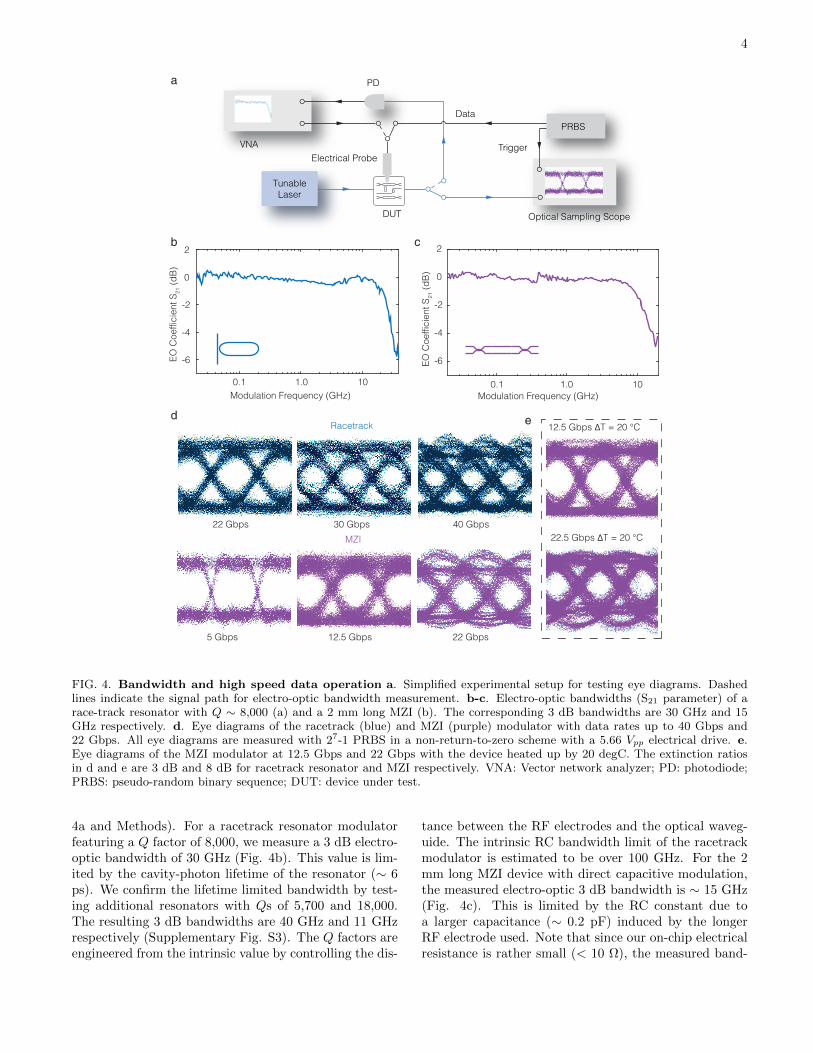
Our miniaturized LN devices exhibit high electro-opticbandwidths (S21 parameter), which we characterize us-ing a network analyzer and a high-speed photodiode (Fig.
4
c
d e
-6
-4
-2
0
2
0.1 1.0 10
-6
-4
-2
0
2
EO
Coe
ffici
ent S
21 (
dB
)
b
EO
Coe
ffici
ent S
21 (
dB
)
Modulation Frequency (GHz)Modulation Frequency (GHz)
DUT
PD
Data
Trigger
Optical Sampling Scope
Electrical Probe
PRBS
TunableLaser
VNA
a
22 Gbps 30 Gbps 40 Gbps
12.5 Gbps ∆T = 20 °C
22.5 Gbps ∆T = 20 °C
Racetrack
0.1 1.0 10
5 Gbps 12.5 Gbps 22 Gbps
MZI
FIG. 4. Bandwidth and high speed data operation a. Simplified experimental setup for testing eye diagrams. Dashedlines indicate the signal path for electro-optic bandwidth measurement. b-c. Electro-optic bandwidths (S21 parameter) of arace-track resonator with Q ∼ 8,000 (a) and a 2 mm long MZI (b). The corresponding 3 dB bandwidths are 30 GHz and 15GHz respectively. d. Eye diagrams of the racetrack (blue) and MZI (purple) modulator with data rates up to 40 Gbps and22 Gbps. All eye diagrams are measured with 27-1 PRBS in a non-return-to-zero scheme with a 5.66 Vpp electrical drive. e.Eye diagrams of the MZI modulator at 12.5 Gbps and 22 Gbps with the device heated up by 20 degC. The extinction ratiosin d and e are 3 dB and 8 dB for racetrack resonator and MZI respectively. VNA: Vector network analyzer; PD: photodiode;PRBS: pseudo-random binary sequence; DUT: device under test.
4a and Methods). For a racetrack resonator modulatorfeaturing a Q factor of 8,000, we measure a 3 dB electro-optic bandwidth of 30 GHz (Fig. 4b). This value is lim-ited by the cavity-photon lifetime of the resonator (∼ 6ps). We confirm the lifetime limited bandwidth by test-ing additional resonators with Qs of 5,700 and 18,000.The resulting 3 dB bandwidths are 40 GHz and 11 GHzrespectively (Supplementary Fig. S3). The Q factors areengineered from the intrinsic value by controlling the dis-
tance between the RF electrodes and the optical waveg-uide. The intrinsic RC bandwidth limit of the racetrackmodulator is estimated to be over 100 GHz. For the 2mm long MZI device with direct capacitive modulation,the measured electro-optic 3 dB bandwidth is ∼ 15 GHz(Fig. 4c). This is limited by the RC constant due toa larger capacitance (∼ 0.2 pF) induced by the longerRF electrode used. Note that since our on-chip electricalresistance is rather small (< 10 Ω), the measured band-
5
width is currently limited by the 50 Ω impedance of thenetwork analyzer drive.
Our platform supports data transmission rates as highas 40 Gbps. Figure 4d displays non-return-to-zero (NRZ)open eye diagrams for both racetrack and MZI modula-tors at various data rates, obtained with 27−1 (pseudo-)random binary sequence at 5.66 Vpp (Methods). Becauseof the high signal quality, our devices can generally oper-ate at data rates 1.5 times their 3 dB bandwidth, whichtranslates to 40 Gbps and 22 Gbps for the racetrack andMZI devices respectively. The measured extinction ra-tios of our modulators are 3 dB and 8 dB with powerconsumptions (CV2/4) of 240 fJ/bit and 1.6 pJ/bit re-spectively.
We confirm that our MZI modulator maintains thestable thermal properties of their bulk counterparts,due to the low thermo-optic coefficient of LN (3.9×10⁻⁵K−1)[3]. We vary the temperature of our chipwithin a ∆T = 20 C range, limited by the setup, andrecord the eye diagrams. We find that the MZI mod-ulator is able to maintain an open eye diagram at themaximum data rate of 22 Gbps without any feedback tocompensate for temperature drifts (open loop configura-tion) (Fig. 4e).
Our micrometer scale LN modulators feature high-bandwidth, excellent linearity, low voltage and good tem-perature stability. The monolithic LN photonic plat-form that we demonstrate here could lead to a paradigmshift in electro-optic modulator scalabilty, performanceand design. For nearly a decade, existing LN modula-tor performance has been capped due to the non-idealphase matching between the RF and optical fields [2].The high dielectric constant of LN (εRF ∼ 28) dictatesthat RF fields in LN propagate much slower than op-tical fields (εopt ∼ 4) resulting in performane trade-offbetween bandwidth and driving voltage [2]. In our thin-film monolithic LN approach, instead, phase matchingcan be much better achieved since the electrical fieldprimarily resides in the low dielectric SiO2 (εopt ∼ 4)and readily propagates at nearly the same group veloc-ity as light [2]. The thin-film micro-MZI modulators,with a phase-matched RF transmission line architecture,could simultaneously achieve ultra-high bandwidth (> 60GHz) and low modulation voltage (∼ 1 V), and thereforeare directly drivable with CMOS circuitry. The activemicro-resonators and low loss waveguides could enable achip-scale photonic circuit densely integrated with novelswitches, filters, nonlinear wavelength sources and oper-ates in a wide wavelength range (from visible to mid-IR).Furthermore, the ultra-compact footprint (as small as 30µm × 30 µm) of micro-ring modulators is attractive fordata center applications where real estate is at a pre-mium. Our high-performance monolithic LN nanopho-tonic platform could become a practical cost-effective so-lution to meet the growing demands of next-generationdata center, metro and long-haul optical telecommunica-
tions.
The authors thank J. Kahn for valuable discussionsand H. Majedi for the use of VNA. This work is supportedin part by the National Science Foundation (ECCS-1609549), Office of Naval Research MURI (N00014-15-1-2761) and Army Research Laboratory Center for Dis-tributed Quantum Information (W911NF1520067). B.S.acknowledge support from the National Science Foun-dation - CIAN ERC (EEC-0812072). Device fabricationwas performed at the center for nanoscale systems (CNS)at Harvard University.
[1] E. L. Wooten, K. M. Kissa, A. Yi-Yan, E. J. Murphy,D. A. Lafaw, P. F. Hallemeier, D. Maack, D. V. Attana-sio, D. J. Fritz, G. J. McBrien, and D. E. Bossi, SelectedTopics in Quantum Electronics, IEEE Journal of 6, 69(2000).
[2] D. Janner, D. Tulli, M. Garca-Granda, M. Belmonte,and V. Pruneri, Laser & Photonics Reviews 3, 301 (2009).
[3] D. N. Nikogosyan, Nonlinear Optical Crystals: A Com-plete Survey (Springer-Science, New York, 2005).
[4] Q. Xu, B. Schmidt, S. Pradhan, and M. Lipson, Nature435, 325 (2005).
[5] E. Timurdogan, C. M. Sorace-Agaskar, J. Sun,E. Shah Hosseini, A. Biberman, and M. R. Watts, Na-ture Communications 5, 4008 (2014).
[6] C. Zhang, P. A. Morton, J. B. Khurgin, J. D. Peters, andJ. E. Bowers, Optica 3, 1483 (2016).
[7] C. Sun, M. T. Wade, Y. Lee, J. S. Orcutt, L. Alloatti,M. S. Georgas, A. S. Waterman, J. M. Shainline, R. R.Avizienis, S. Lin, B. R. Moss, R. Kumar, F. Pavanello,A. H. Atabaki, H. M. Cook, A. J. Ou, J. C. Leu, Y.-H.Chen, K. Asanovi, R. J. Ram, M. A. Popovi, and V. M.Stojanovi, Nature 528, 534 (2015).
[8] C. Rolland, R. S. Moore, F. Shepherd, and G. Hillier,Electronics Letters 29, 471 (1993).
[9] M. Aoki, M. Suzuki, H. Sano, T. Kawano, T. Ido,T. Taniwatari, K. Uomi, and A. Takai, IEEE Journalof Quantum Electronics 29, 2088 (1993).
[10] N. Kikuchi, E. Yamada, Y. Shibata, and H. Ishii, in2012 IEEE Compound Semiconductor Integrated CircuitSymposium (CSICS) (2012) pp. 1–4.
[11] C. Xiong, W. H. P. Pernice, and H. X. Tang, Nano Let-ters 12, 3562 (2012).
[12] HaffnerC, HeniW, FedoryshynY, NiegemannJ, Me-likyanA, D. L. Elder, BaeuerleB, SalaminY, JostenA,KochU, HoessbacherC, DucryF, JuchliL, EmborasA,HillerkussD, KohlM, L. R. Dalton, HafnerC, andLeutholdJ, Nat Photon 9, 525 (2015).
[13] M. Liu, X. Yin, E. Ulin-Avila, B. Geng, T. Zentgraf,L. Ju, F. Wang, and X. Zhang, Nature 474, 64 (2011).
[14] C. T. Phare, Y.-H. Daniel Lee, J. Cardenas, and M. Lip-son, Nat Photon 9, 511 (2015).
[15] K. S. Novoselov, V. I. Falko, L. Colombo, P. R. Gellert,M. G. Schwab, and K. Kim, Nature 490, 192 (2012).
[16] M. Lee, H. E. Katz, C. Erben, D. M. Gill, P. Gopalan,J. D. Heber, and D. J. McGee, Science 298, 1401 (2002).
[17] J. Clark and G. Lanzani, Nat Photon 4, 438 (2010).[18] R. V. Schmidt and I. P. Kaminow, Applied Physics Let-
6
ters 25, 458 (1974).[19] G. Poberaj, H. Hu, W. Sohler, and P. Gnter, Laser &
Photonics Reviews 6, 488 (2012).[20] A. Guarino, G. Poberaj, D. Rezzonico, R. Degl’Innocenti,
and P. Gunter, Nat Photon 1, 407 (2007).[21] L. Chen, Q. Xu, M. G. Wood, and R. M. Reano, Optica
1, 112 (2014).[22] A. Rao, A. Patil, J. Chiles, M. Malinowski, S. Novak,
K. Richardson, P. Rabiei, and S. Fathpour, Optics Ex-press 23, 22746 (2015).
[23] S. Jin, L. Xu, H. Zhang, and Y. Li, IEEE PhotonicsTechnology Letters 28, 736 (2016).
[24] A. Rao, A. Patil, P. Rabiei, A. Honardoost, R. DeSalvo,A. Paolella, and S. Fathpour, Optics Letters 41, 5700(2016).
[25] J. Wang, F. Bo, S. Wan, W. Li, F. Gao, J. Li, G. Zhang,and J. Xu, Optics Express 23, 23072 (2015).
[26] L. Cai, Y. Kang, and H. Hu, Optics Express 24, 4640(2016).
[27] C. Wang, M. J. Burek, Z. Lin, H. A. Atikian,V. Venkataraman, I. C. Huang, P. Stark, and M. Lonar,Optics Express 22, 30924 (2014).
[28] C. Wang, X. Xiong, N. Andrade, V. Venkataraman,X.-F. Ren, G.-C. Guo, and M. Lonar, arXiv preprintarXiv:1610.04197 (2016).
[29] L. Chang, Y. Li, N. Volet, L. Wang, J. Peters, and J. E.Bowers, Optica 3, 531 (2016).
[30] V. S. Ilchenko, A. A. Savchenkov, A. B. Matsko, andL. Maleki, Physical Review Letters 92, 043903 (2004).