Using Metamaterial-Based Coplanar Waveguide Structures for ...
General rights Copyright and moral rights for the publications made accessible in the public portal are retained by the authors and/or other copyright owners and it is a condition of accessing publications that users recognise and abide by the legal requirements associated with these rights.
• Users may download and print one copy of any publication from the public portal for the purpose of private study or research. • You may not further distribute the material or use it for any profit-making activity or commercial gain • You may freely distribute the URL identifying the publication in the public portal
If you believe that this document breaches copyright please contact us providing details, and we will remove access to the work immediately and investigate your claim.
Downloaded from orbit.dtu.dk on: Jun 12, 2018
Rectangular waveguide-to-coplanar waveguide transitions at U-band using e-planeprobe and wire bonding
Dong, Yunfeng; Johansen, Tom Keinicke; Zhurbenko, Vitaliy; Hanberg, Peter Jesper
Published in:Proceedings of the 46th European Microwave Conference
Link to article, DOI:10.1109/EuMC.2016.7824263
Publication date:2016
Document VersionPeer reviewed version
Link back to DTU Orbit
Citation (APA):Dong, Y., Johansen, T. K., Zhurbenko, V., & Hanberg, P. J. (2016). Rectangular waveguide-to-coplanarwaveguide transitions at U-band using e-plane probe and wire bonding. In Proceedings of the 46th EuropeanMicrowave Conference (pp. 5-8). IEEE. (2016 46th European Microwave Conference (eumc)). DOI:10.1109/EuMC.2016.7824263
Rectangular Waveguide-to-Coplanar WaveguideTransitions at U-Band Using E-Plane Probe and
Wire Bonding
Yunfeng Dong, Tom K. Johansen, Vitaliy ZhurbenkoElectromagnetic System, Department of Electrical Engineering
Technical University of Denmark
DK-2800 Kgs. Lyngby, Denmark
yundon/tkj/[email protected]
Peter Jesper HanbergDTU Danchip
Technical University of Denmark
DK-2800 Kgs. Lyngby, Denmark
Abstract—This paper presents rectangular waveguide-to-coplanar waveguide (CPW) transitions at U-band (40 – 60 GHz)using E-plane probe and wire bonding. The designs of CPWsbased on quartz substrate with and without aluminum cover areexplained. The single and double layer rectangular waveguide-to-CPW transitions using E-plane probe and wire bonding aredesigned. The proposed rectangular waveguide-to-CPW transi-tion using wire bonding can provide 10 GHz bandwidth at U-band and does not require extra CPWs or connections betweenCPWs and chips. A single layer rectangular waveguide-to-CPWtransition using E-plane probe with aluminum package has beenfabricated and measured to validate the proposed transitions. Tothe authors’ best knowledge, this is the first time that a wirebonding is used as a probe for rectangular waveguide-to-CPWtransition at U-band.
I. INTRODUCTION
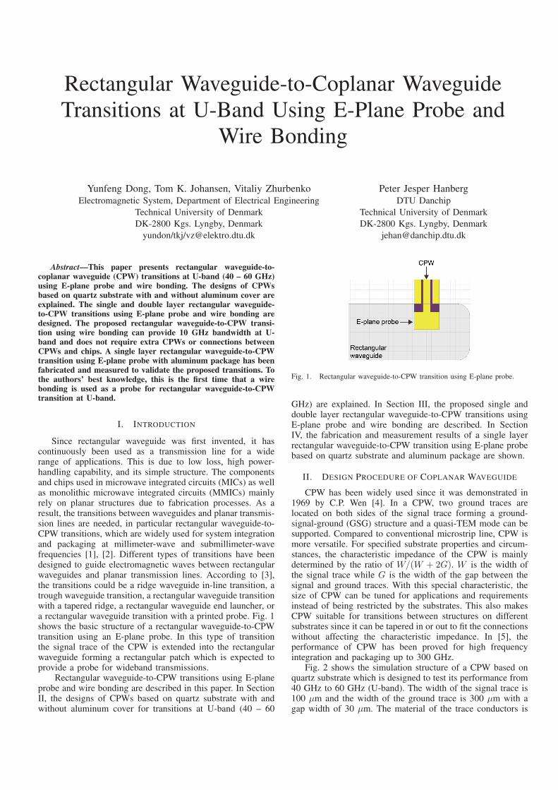
Since rectangular waveguide was first invented, it hascontinuously been used as a transmission line for a widerange of applications. This is due to low loss, high power-handling capability, and its simple structure. The componentsand chips used in microwave integrated circuits (MICs) as wellas monolithic microwave integrated circuits (MMICs) mainlyrely on planar structures due to fabrication processes. As aresult, the transitions between waveguides and planar transmis-sion lines are needed, in particular rectangular waveguide-to-CPW transitions, which are widely used for system integrationand packaging at millimeter-wave and submillimeter-wavefrequencies [1], [2]. Different types of transitions have beendesigned to guide electromagnetic waves between rectangularwaveguides and planar transmission lines. According to [3],the transitions could be a ridge waveguide in-line transition, atrough waveguide transition, a rectangular waveguide transitionwith a tapered ridge, a rectangular waveguide end launcher, ora rectangular waveguide transition with a printed probe. Fig. 1shows the basic structure of a rectangular waveguide-to-CPWtransition using an E-plane probe. In this type of transitionthe signal trace of the CPW is extended into the rectangularwaveguide forming a rectangular patch which is expected toprovide a probe for wideband transmissions.
Rectangular waveguide-to-CPW transitions using E-planeprobe and wire bonding are described in this paper. In SectionII, the designs of CPWs based on quartz substrate with andwithout aluminum cover for transitions at U-band (40 – 60
Fig. 1. Rectangular waveguide-to-CPW transition using E-plane probe.
GHz) are explained. In Section III, the proposed single anddouble layer rectangular waveguide-to-CPW transitions usingE-plane probe and wire bonding are described. In SectionIV, the fabrication and measurement results of a single layerrectangular waveguide-to-CPW transition using E-plane probebased on quartz substrate and aluminum package are shown.
II. DESIGN PROCEDURE OF COPLANAR WAVEGUIDE
CPW has been widely used since it was demonstrated in1969 by C.P. Wen [4]. In a CPW, two ground traces arelocated on both sides of the signal trace forming a ground-signal-ground (GSG) structure and a quasi-TEM mode can besupported. Compared to conventional microstrip line, CPW ismore versatile. For specified substrate properties and circum-stances, the characteristic impedance of the CPW is mainlydetermined by the ratio of W/(W + 2G). W is the width ofthe signal trace while G is the width of the gap between thesignal and ground traces. With this special characteristic, thesize of CPW can be tuned for applications and requirementsinstead of being restricted by the substrates. This also makesCPW suitable for transitions between structures on differentsubstrates since it can be tapered in or out to fit the connectionswithout affecting the characteristic impedance. In [5], theperformance of CPW has been proved for high frequencyintegration and packaging up to 300 GHz.
Fig. 2 shows the simulation structure of a CPW based onquartz substrate which is designed to test its performance from40 GHz to 60 GHz (U-band). The width of the signal trace is100 μm and the width of the ground trace is 300 μm with agap width of 30 μm. The material of the trace conductors is
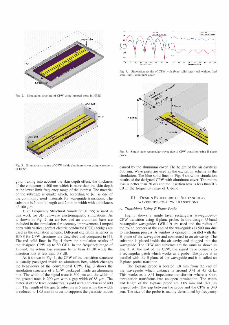
Fig. 2. Simulation structure of CPW using lumped ports in HFSS.
Fig. 3. Simulation structure of CPW inside aluminum cover using wave portsin HFSS.
gold. Taking into account the skin depth effect, the thicknessof the conductor is 400 nm which is more than the skin depthat the lower limit frequency range of the interest. The materialof the substrate is quartz which, according to [6], is one ofthe commonly used materials for waveguide transitions. Thesubstrate is 5 mm in length and 2 mm in width with a thicknessof 160 μm.
High Frequency Structural Simulator (HFSS) is used inthis work for 3D full-wave electromagnetic simulations. Asit shown in Fig. 2, an air box and an aluminum base areincluded in the simulation for accuracy improvement. Lumpedports with vertical perfect electric conductor (PEC) bridges areused as the excitation scheme. Different excitation schemes inHFSS for CPW structures are described and compared in [7].The red solid lines in Fig. 4 show the simulation results ofthe designed CPW up to 80 GHz. In the frequency range ofU-band, the return loss remains better than 15 dB while theinsertion loss is less than 0.8 dB.
As it shown in Fig. 1, the CPW of the transition structureis usually packaged inside an aluminum box, which changesthe behaviours of the conventional CPW. Fig. 3 shows thesimulation structure of a CPW packaged inside an aluminumbox. The width of the signal trace is 300 μm and the width ofthe ground trace is 290 μm with a gap width of 85 μm. Thematerial of the trace conductors is gold with a thickness of 400nm. The length of the quartz substrate is 5 mm while the widthis reduced to 1.05 mm in order to suppress the parasitic modes
Fig. 4. Simulation results of CPW with (blue solid lines) and without (redsolid lines) aluminum cover.
Fig. 5. Single layer rectangular waveguide-to-CPW transition using E-planeprobe.
caused by the aluminum cover. The height of the air cavity is500 μm. Wave ports are used as the excitation scheme in thesimulation. The blue solid lines in Fig. 4 show the simulationresults of the designed CPW with aluminum cover. The returnloss is better than 20 dB and the insertion loss is less than 0.3dB in the frequency range of U-band.
III. DESIGN PROCEDURE OF RECTANGULAR
WAVEGUIDE-TO-CPW TRANSITIONS
A. Transitions Using E-Plane Probe
Fig. 5 shows a single layer rectangular waveguide-to-CPW transition using E-plane probe. In this design, U-bandrectangular waveguides (WR-19) are used and the radius ofthe round corners at the end of the waveguides is 500 um dueto machining process. A window is opened in parallel with theH-plane of the waveguide and connected to an air cavity. Thesubstrate is placed inside the air cavity and plugged into thewaveguide. The CPW and substrate are the same as shown inFig. 3. At the end of the CPW, the signal trace connects toa rectangular patch which works as a probe. The probe is inparallel with the E-plane of the waveguide and it is called anE-plane probe transition.
The E-plane probe is located 1.8 mm from the end ofthe waveguide which distance is around λ/4 at 45 GHz.This works as a λ/4 impedance transformer where a shorttermination transforms into an open termination. The widthand length of the E-plane probe are 1.05 mm and 740 μmrespectively. The gap between the probe and the CPW is 340μm. The size of the probe is mainly determined by frequency
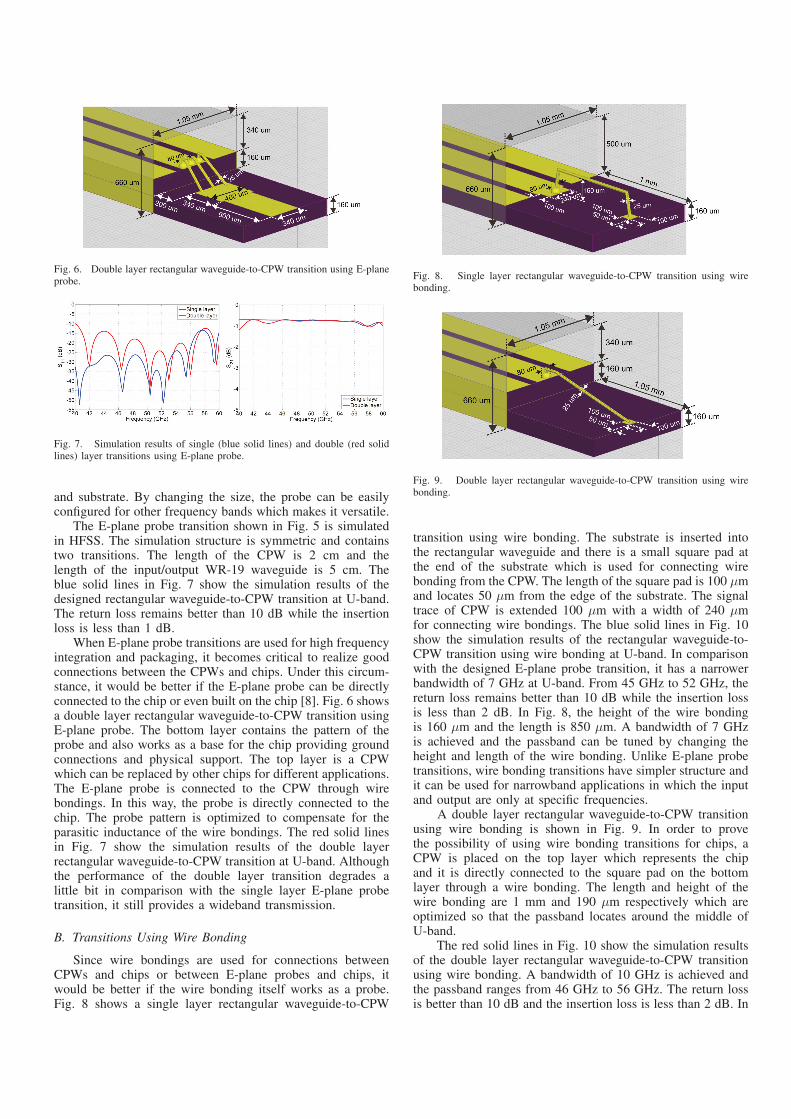
Fig. 6. Double layer rectangular waveguide-to-CPW transition using E-planeprobe.
Fig. 7. Simulation results of single (blue solid lines) and double (red solidlines) layer transitions using E-plane probe.
and substrate. By changing the size, the probe can be easilyconfigured for other frequency bands which makes it versatile.
The E-plane probe transition shown in Fig. 5 is simulatedin HFSS. The simulation structure is symmetric and containstwo transitions. The length of the CPW is 2 cm and thelength of the input/output WR-19 waveguide is 5 cm. Theblue solid lines in Fig. 7 show the simulation results of thedesigned rectangular waveguide-to-CPW transition at U-band.The return loss remains better than 10 dB while the insertionloss is less than 1 dB.
When E-plane probe transitions are used for high frequencyintegration and packaging, it becomes critical to realize goodconnections between the CPWs and chips. Under this circum-stance, it would be better if the E-plane probe can be directlyconnected to the chip or even built on the chip [8]. Fig. 6 showsa double layer rectangular waveguide-to-CPW transition usingE-plane probe. The bottom layer contains the pattern of theprobe and also works as a base for the chip providing groundconnections and physical support. The top layer is a CPWwhich can be replaced by other chips for different applications.The E-plane probe is connected to the CPW through wirebondings. In this way, the probe is directly connected to thechip. The probe pattern is optimized to compensate for theparasitic inductance of the wire bondings. The red solid linesin Fig. 7 show the simulation results of the double layerrectangular waveguide-to-CPW transition at U-band. Althoughthe performance of the double layer transition degrades alittle bit in comparison with the single layer E-plane probetransition, it still provides a wideband transmission.
B. Transitions Using Wire Bonding
Since wire bondings are used for connections betweenCPWs and chips or between E-plane probes and chips, itwould be better if the wire bonding itself works as a probe.Fig. 8 shows a single layer rectangular waveguide-to-CPW
Fig. 8. Single layer rectangular waveguide-to-CPW transition using wirebonding.
Fig. 9. Double layer rectangular waveguide-to-CPW transition using wirebonding.
transition using wire bonding. The substrate is inserted intothe rectangular waveguide and there is a small square pad atthe end of the substrate which is used for connecting wirebonding from the CPW. The length of the square pad is 100 μmand locates 50 μm from the edge of the substrate. The signaltrace of CPW is extended 100 μm with a width of 240 μmfor connecting wire bondings. The blue solid lines in Fig. 10show the simulation results of the rectangular waveguide-to-CPW transition using wire bonding at U-band. In comparisonwith the designed E-plane probe transition, it has a narrowerbandwidth of 7 GHz at U-band. From 45 GHz to 52 GHz, thereturn loss remains better than 10 dB while the insertion lossis less than 2 dB. In Fig. 8, the height of the wire bondingis 160 μm and the length is 850 μm. A bandwidth of 7 GHzis achieved and the passband can be tuned by changing theheight and length of the wire bonding. Unlike E-plane probetransitions, wire bonding transitions have simpler structure andit can be used for narrowband applications in which the inputand output are only at specific frequencies.
A double layer rectangular waveguide-to-CPW transitionusing wire bonding is shown in Fig. 9. In order to provethe possibility of using wire bonding transitions for chips, aCPW is placed on the top layer which represents the chipand it is directly connected to the square pad on the bottomlayer through a wire bonding. The length and height of thewire bonding are 1 mm and 190 μm respectively which areoptimized so that the passband locates around the middle ofU-band.
The red solid lines in Fig. 10 show the simulation resultsof the double layer rectangular waveguide-to-CPW transitionusing wire bonding. A bandwidth of 10 GHz is achieved andthe passband ranges from 46 GHz to 56 GHz. The return lossis better than 10 dB and the insertion loss is less than 2 dB. In
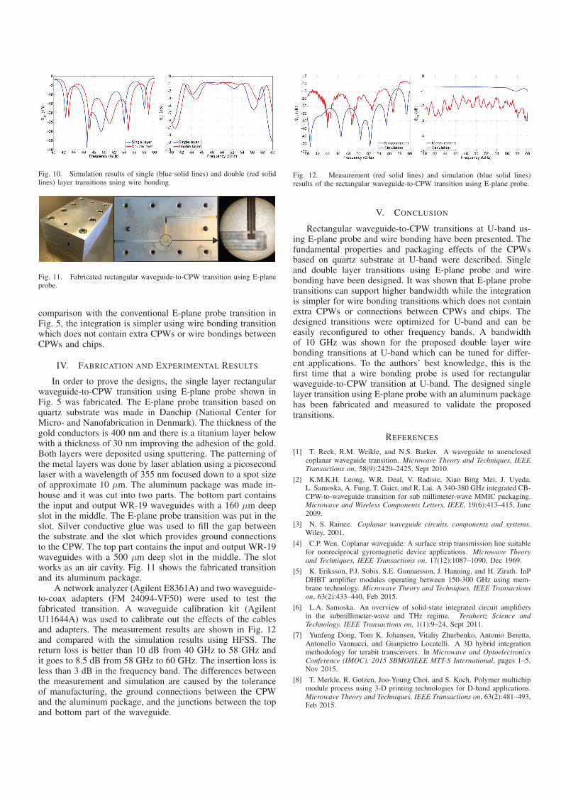
Fig. 10. Simulation results of single (blue solid lines) and double (red solidlines) layer transitions using wire bonding.
Fig. 11. Fabricated rectangular waveguide-to-CPW transition using E-planeprobe.
comparison with the conventional E-plane probe transition inFig. 5, the integration is simpler using wire bonding transitionwhich does not contain extra CPWs or wire bondings betweenCPWs and chips.
IV. FABRICATION AND EXPERIMENTAL RESULTS
In order to prove the designs, the single layer rectangularwaveguide-to-CPW transition using E-plane probe shown inFig. 5 was fabricated. The E-plane probe transition based onquartz substrate was made in Danchip (National Center forMicro- and Nanofabrication in Denmark). The thickness of thegold conductors is 400 nm and there is a titanium layer belowwith a thickness of 30 nm improving the adhesion of the gold.Both layers were deposited using sputtering. The patterning ofthe metal layers was done by laser ablation using a picosecondlaser with a wavelength of 355 nm focused down to a spot sizeof approximate 10 μm. The aluminum package was made in-house and it was cut into two parts. The bottom part containsthe input and output WR-19 waveguides with a 160 μm deepslot in the middle. The E-plane probe transition was put in theslot. Silver conductive glue was used to fill the gap betweenthe substrate and the slot which provides ground connectionsto the CPW. The top part contains the input and output WR-19waveguides with a 500 μm deep slot in the middle. The slotworks as an air cavity. Fig. 11 shows the fabricated transitionand its aluminum package.
A network analyzer (Agilent E8361A) and two waveguide-to-coax adapters (FM 24094-VF50) were used to test thefabricated transition. A waveguide calibration kit (AgilentU11644A) was used to calibrate out the effects of the cablesand adapters. The measurement results are shown in Fig. 12and compared with the simulation results using HFSS. Thereturn loss is better than 10 dB from 40 GHz to 58 GHz andit goes to 8.5 dB from 58 GHz to 60 GHz. The insertion loss isless than 3 dB in the frequency band. The differences betweenthe measurement and simulation are caused by the toleranceof manufacturing, the ground connections between the CPWand the aluminum package, and the junctions between the topand bottom part of the waveguide.
Fig. 12. Measurement (red solid lines) and simulation (blue solid lines)results of the rectangular waveguide-to-CPW transition using E-plane probe.
V. CONCLUSION
Rectangular waveguide-to-CPW transitions at U-band us-ing E-plane probe and wire bonding have been presented. Thefundamental properties and packaging effects of the CPWsbased on quartz substrate at U-band were described. Singleand double layer transitions using E-plane probe and wirebonding have been designed. It was shown that E-plane probetransitions can support higher bandwidth while the integrationis simpler for wire bonding transitions which does not containextra CPWs or connections between CPWs and chips. Thedesigned transitions were optimized for U-band and can beeasily reconfigured to other frequency bands. A bandwidthof 10 GHz was shown for the proposed double layer wirebonding transitions at U-band which can be tuned for differ-ent applications. To the authors’ best knowledge, this is thefirst time that a wire bonding probe is used for rectangularwaveguide-to-CPW transition at U-band. The designed singlelayer transition using E-plane probe with an aluminum packagehas been fabricated and measured to validate the proposedtransitions.
REFERENCES
[1] T. Reck, R.M. Weikle, and N.S. Barker. A waveguide to unenclosedcoplanar waveguide transition. Microwave Theory and Techniques, IEEETransactions on, 58(9):2420–2425, Sept 2010.
[2] K.M.K.H. Leong, W.R. Deal, V. Radisic, Xiao Bing Mei, J. Uyeda,L. Samoska, A. Fung, T. Gaier, and R. Lai. A 340-380 GHz integrated CB-CPW-to-waveguide transition for sub millimeter-wave MMIC packaging.Microwave and Wireless Components Letters, IEEE, 19(6):413–415, June2009.
[3] N. S. Rainee. Coplanar waveguide circuits, components and systems.Wiley, 2001.
[4] C.P. Wen. Coplanar waveguide: A surface strip transmission line suitablefor nonreciprocal gyromagnetic device applications. Microwave Theoryand Techniques, IEEE Transactions on, 17(12):1087–1090, Dec 1969.
[5] K. Eriksson, P.J. Sobis, S.E. Gunnarsson, J. Hanning, and H. Zirath. InPDHBT amplifier modules operating between 150-300 GHz using mem-brane technology. Microwave Theory and Techniques, IEEE Transactionson, 63(2):433–440, Feb 2015.
[6] L.A. Samoska. An overview of solid-state integrated circuit amplifiersin the submillimeter-wave and THz regime. Terahertz Science andTechnology, IEEE Transactions on, 1(1):9–24, Sept 2011.
[7] Yunfeng Dong, Tom K. Johansen, Vitaliy Zhurbenko, Antonio Beretta,Antonello Vannucci, and Gianpietro Locatelli. A 3D hybrid integrationmethodology for terabit transceivers. In Microwave and OptoelectronicsConference (IMOC), 2015 SBMO/IEEE MTT-S International, pages 1–5,Nov 2015.
[8] T. Merkle, R. Gotzen, Joo-Young Choi, and S. Koch. Polymer multichipmodule process using 3-D printing technologies for D-band applications.Microwave Theory and Techniques, IEEE Transactions on, 63(2):481–493,Feb 2015.