MSER-FPD 1
12
MSER-FPD 1.20
Transcript of MSER-FPD 1

MSER-FPD 1.20

MSER-FPD 1.20 2
Table of Contents
1. Introduction 3
2. MSER-FPD Rev 1.20 42.1 FAKRA Connector ........................................................................................................... 4
2.2 Flex Cable Connection with Stiffener on the MSER-FPD ............................................. 5
2.3 I/O Signals of MSER-FPD ................................................................................................ 8
2.4 I2C I/O Expander Configuration .................................................................................... 9
2.5 I/O Connector ............................................................................................................... 10
2.6 On-board LEDs .............................................................................................................. 11

MSER-FPD 1.20 3
Introduction
1 Introduction
This document describes the function of the MSER-FPD MIPI serializer board which is based
on the Texas Instruments MIPI-CSI-2-to-FPD-Link III serializer chip, DS90UB953-Q1. The
camera-side serializer board and platform-side deserializer board enable distances of up to
15m between any TISMIPI sensor and embedded system using a coaxial cable. The
connection of these components is shown below:
The document "Deserializer Design Recommendations" contains important information
required to create a custom deserializer design using the TI DS90UB954-Q1 chip.
MSER-FPD 1.20 4
MSER-FPD Rev 1.20
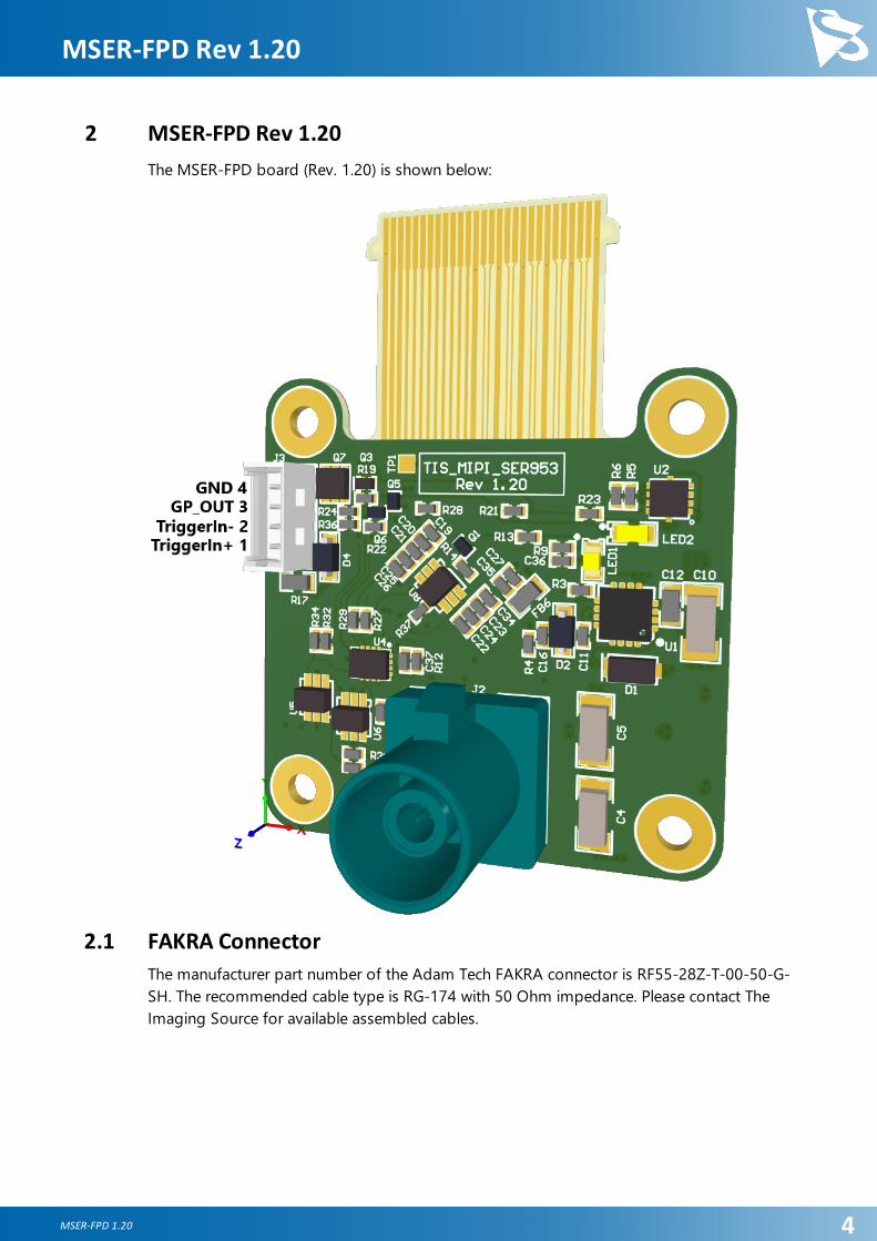
2 MSER-FPD Rev 1.20
The MSER-FPD board (Rev. 1.20) is shown below:
2.1 FAKRA Connector
The manufacturer part number of the Adam Tech FAKRA connector is RF55-28Z-T-00-50-G-
SH. The recommended cable type is RG-174 with 50 Ohm impedance. Please contact The
Imaging Source for available assembled cables.

MSER-FPD 1.20 5
MSER-FPD Rev 1.20
2.2 Flex Cable Connection with Stiffener on the MSER-FPD
The flex cable connection with stiffener has the following pinout:

MSER-FPD 1.20 6
MSER-FPD Rev 1.20
# Name Type Description
1 GND GND Ground
2 MIPI_CH3_N I MIPI CSI-2 input
3 MIPI_CH3_P I MIPI CSI-2 input
4 GND GND Ground
5 MIPI_CH1_N I MIPI CSI-2 input
6 MIPI_CH1_P I MIPI CSI-2 input
7 GND GND Ground
8 MIPI_DCK_N I MIPI CSI-2 input
9 MIPI_DCK_P I MIPI CSI-2 input
10 GND GND Ground
11 MIPI_CH2_N I MIPI CSI-2 input
12 MIPI_CH2_P I MIPI CSI-2 input
13 GND GND Ground
14 MIPI_CH4_N I MIPI CSI-2 input
15 MIPI_CH4_P I MIPI CSI-2 input
16 GND GND Ground
17 CLK O Reference clock output
18 CAM_PWR O High active camera power enable signal
19 I2C_SCL I/O I2C serial clock
20 I2C_SDA I/O I2C serial data
21 RESERVED_1 I/O Reserved pin 1
22 RESET O Reset sensor to default state when low
23 RESERVED_2 I/O Reserved pin 2
24 STROBE I CMOS sensor strobe signal input
25 TRIGGER/FSYNC O Trigger signal output
26 +5V_VDD PWR 5V (±10%) power supply

MSER-FPD 1.20 7
MSER-FPD Rev 1.20
# Name Type Description
27 +5V_VDD PWR 5V (±10%) power supply
28 GND GND Ground

MSER-FPD 1.20 8
MSER-FPD Rev 1.20
2.3 I/O Signals of MSER-FPD
The connected I/O signals on the serializer chip DS90UB953-Q1 (Texas Instruments) are
listed in the following table:
Pin Name Dir Description
17 (GPIO0) STROBE I Strobe signal from sensor board
18 (GPIO1) TRIGGER_SER I External trigger signal from serializer board
27 (GPOI2) TRIGGER O Trigger signal from deserializer board
28 (GPOI3) RESERVED1_
GPIO3
I/O Reserved signal
Since the DS90UB953-Q1 serializer chip does not have enough free I/O-pins, an I2C I/O
expander (Texas Instruments TCA6408A) has been placed on the board. The following table
shows which I/O signals on the flex cable connection are connected directly to the
DS90UB953-Q1 and which signals are controlled by the I2C I/O expander:
Pin Name Dir Description Pin at
DS90UB953
Pin at I2C I/O
Expander
17 CLK O CMOS sensor clock CLK_OUT (19)
18 CAM_PWR O Camera power enable,
active high
Pin 2 (P0)
19 I2C_SCL I/O I2C-Bus, clock I2C_SCL (24)
20 I2C_SDA I/O I2C-Bus, data I2C_SDA (23)
21 RESERVED_1 I/O Reserved GPIO3 (28)
22 RESET O CMOS sensor reset
signal, active low
Pin 3 (P1)
23 RESERVED_2 I/O Reserved Pin 10 (P7)
24 STROBE I CMOS sensor strobe
signal
GPIO0 (17)
25 TRIGGER O CMOS sensor trigger
signal
GPIO2 (27)
All I/Os have the same I/O voltage of 1.8V.

MSER-FPD 1.20 9
MSER-FPD Rev 1.20
2.4 I2C I/O Expander Configuration
The I/O expander TCA6408A has the 7-bit I2C-address 0x20. The table below depicts which
signals can be controlled through this expander:
I/O Pin Name Dir Description
P0 CAM_PWR O Enable CMOS sensor power supply
0: Sensor power disabled
1: Sensor power enabled
P1 RESET O CMOS sensor reset signal
0: Sensor is in reset state
1: Sensor is in operational state
P2 GPOUT_LEVEL O If GPOUT_SELECT = 0:
--->0: LED1 off
--->1: LED1 on
If GPOUT_SELECT = 1:
--->0: GPOUT is low/0 V
--->1: GPOUT is tri-stated or high/+5V (depends on
the setting of GPIO3)
P3 GPOUT_PUSHPULL O GPOUT (PicoBlade) type selection
0: GPOUT is configured as open-drain-output
1: GPOUT is configured as TTL/push-pull-output
P4 GPOUT_SELECT O Function of GPOUT (PicoBlade) Pin
0: STROBE from CMOS sensor board
1: GPOUT_LEVEL from serializer board
P5 TRIGGER_LEVEL O Controls the polarity of the trigger input on the
PicoBlade connector.
0: Trigger source level polarity is not inverted
1: Trigger source level polarity is inverted
P6 TRIGGER_SOURCE O Controls the source of the trigger signal that is
forwarded to the sensor.
0: Sensor is triggered by the trigger signal coming
from the FPD-Link / deserializer chip.
1: Sensor is triggered by the trigger signal that is
applied to the PicoBlade I/O connector.
P7 RESERVED_2 O Reserved

MSER-FPD 1.20 10
MSER-FPD Rev 1.20
2.5 I/O Connector
The serializer also has a user GPIO I/O connector with the following pinout:
Pin Name Description
1 TRIGGER_IN_P Opto-decoupled trigger input, anode of IR-LED
2 TRIGGER_IN_N Opto-decoupled trigger input, cathode of IR-LED
3 GP_OUT General purpose output, referenced to GND
4 GND System ground
The trigger input is opto-decoupled. To drive the trigger input, voltage must be applied to
pins 1 and 2. Note: pin 1 is the positive input; pin 2 is the negative input.
Pin 3 is a general-purpose output pin that can be controlled via software. The pin can be
configured for TTL mode output or open drain output. LED2 indicates a possible
overcurrent.
The recommended operating conditions of the user GPIO connector J3 are displayed in the
following tables. CAUTION: Functional operation beyond the recommended operating
conditions is not assumed.
Parameter Min Max
Trigger input voltage 3.3V ± 5% 24V ± 5%

MSER-FPD 1.20 11
MSER-FPD Rev 1.20
Parameter Min Max
TTL-mode high voltage - 250mA @ 4V
TTL-mode low voltage - 250mA @ 0.05V
Parameter Min Max
Open-drain-mode voltage - 24V
Open-drain-mode current - 250mA
Please make sure that enough additional power is provided via the embedded system to
operate the connected devices at the user GPIO connector (J3).
2.6 On-board LEDs
There are two, status LEDs on the serializer board:
Name Color Description
LED1 Green Controlled through GPOUT_LEVEL on the I/O expander
LED2 Red Indicates overcurrent flowing out of GP_OUT in TTL/push-pull
mode.

MSER-FPD 1.20 12
MSER-FPD 1.20
All product and company names in this document may be trademarks and tradenames of their respective owners and arehereby acknowledged.
The Imaging Source Europe GmbH cannot and does not take any responsibility or liability for any information contained inthis document. The source code presented in this document is exclusively used for didactic purposes. The Imaging SourceEurope GmbH does not assume any kind of warranty expressed or implied, resulting from the use of the content of thisdocument or the source code.
The Imaging Source Europe GmbH reserves the right to make changes in specifications, function or design at any time andwithout prior notice.
Last update: January 2021© 2021 The Imaging Source Europe GmbHAll rights reserved. No part of this publication may be reproduced, distributed, or transmitted in any form or by any means,including photocopying, recording, or other electronic or mechanical methods, without the prior written permission of thepublisher, except in the case of brief quotations embodied in critical reviews and certain other noncommercial usespermitted by copyright law.
All weights and dimensions are approximate. Unless otherwise specified, the lenses shown in the context of cameras arenot shipped with these cameras.
Headquarters:
The Imaging Source Europe GmbHÜberseetor 18, D-28217 Bremen, GermanyPhone: +49 421 33591-0
North & South America:
The Imaging Source, LLC6926 Shannon Willow Rd, S 400, Charlotte, NC 28226, USAPhone: +1 704-370-0110
Asia Pacific:
The Imaging Source Asia Co., Ltd. 2F., No.8, Xinhu 1st Road Taipei City 114, Neihu District, TaiwanPhone: +886 2-2792-3153
www.theimagingsource.com