Modeling and characterization of multiple coupled lines
118
AN ABSTRACT OF THE THESIS OF Alok Tripathi for the degree of Doctor of Philosophy in Electrical and Computer Engineering presented on April 2, 1999. Title: Modeling and Characterization of Multiple Coupled Lines Abstract approved- . K. npat A configuration-oriented circuit model for multiple coupled lines in an inhomoge- neous medium is developed and presented in this thesis. This circuit model consists of a network of uncoupled transmission lines and is readily modeled with simulation tools like LIBRA() and SPICE ©. It provides an equivalent circuit representation which is simple and topologically meaningful as compared to the model based on modal decom- position. The configuration-oriented model is derived by decomposing the immittance matrices associated with an n coupled line 2n-port system. Time- and frequency-domain simulations of typical coupled line multiports are included to exemplify the utility of the model. The model is useful for the simulation and design of general single and multi- layer coupled line components, such as filters and couplers, and for the investigation of signal integrity issues including crosstalk in interconnects associated with high speed digital and mixed signal electronic modules and packages. It is shown that multiconductor lossless structures in an inhomogeneous medium can be characterized by multiport time-domain reflection (TDR) measurements. A syn- thesis technique of an equivalent lossless (non-dispersive) uniform multiconductor n coupled lines (UMCL) 2n-port system from the measured discrete time-domain reflec- tion response is presented. This procedure is based on the decomposition of the charac- teristic immittance matrices of the UMCL in terms of partial mode immittance matrices. The decomposition scheme leads to the discrete transition matrix function of a UMCL 2n-port system. This in turn establishes a relationship between the normal-mode pa- rameters of the UMCL and the measured impulse reflection and transmission response. Equivalence between the synthesis procedure presented in this thesis and the solution
Transcript of Modeling and characterization of multiple coupled lines

AN ABSTRACT OF THE THESIS OF
Alok Tripathi for the degree of Doctor of Philosophy in Electrical and Computer
Engineering presented on April 2 1999
Title Modeling and Characterization of Multiple Coupled Lines
Abstract approved-
K npat
A configuration-oriented circuit model for multiple coupled lines in an inhomoge-
neous medium is developed and presented in this thesis This circuit model consists of
a network of uncoupled transmission lines and is readily modeled with simulation tools
like LIBRA() and SPICE copy It provides an equivalent circuit representation which is
simple and topologically meaningful as compared to the model based on modal decom-
position The configuration-oriented model is derived by decomposing the immittance
matrices associated with an n coupled line 2n-port system Time- and frequency-domain
simulations of typical coupled line multiports are included to exemplify the utility of the
model The model is useful for the simulation and design of general single and multi-
layer coupled line components such as filters and couplers and for the investigation of
signal integrity issues including crosstalk in interconnects associated with high speed
digital and mixed signal electronic modules and packages
It is shown that multiconductor lossless structures in an inhomogeneous medium
can be characterized by multiport time-domain reflection (TDR) measurements A syn-
thesis technique of an equivalent lossless (non-dispersive) uniform multiconductor n
coupled lines (UMCL) 2n-port system from the measured discrete time-domain reflec-
tion response is presented This procedure is based on the decomposition of the charac-
teristic immittance matrices of the UMCL in terms of partial mode immittance matrices
The decomposition scheme leads to the discrete transition matrix function of a UMCL
2n-port system This in turn establishes a relationship between the normal-mode pa-
rameters of the UMCL and the measured impulse reflection and transmission response
Equivalence between the synthesis procedure presented in this thesis and the solution
of a special form of an algebraic Riccati matrix equation whose solution can lead to
the normal-mode parameters and a real termination network is illustrated In order to
demonstrate the procedure a typical microstrip structure with three lines is synthesized
from the time-domain reflection (TDR) data
In order to compliment known field theoretic techniques for characterization of mul-
ticonductor structures a network analog method is employed to solve the magnetic vec-
tor potential equation to characterize multilayer Metal-Insulator-Semiconductor (MIS)
transmission line structures This approach leads to the frequency dependent distributed
inductance and the resistance matrices of a multilayer MIS transmission line structure It
is shown that the frequency dependent transmission line parameters can be modeled by
an efficient quasi-static formulation for all propagating modes including the slow-wave
and skin-effect modes To demonstrate the proposed approach for single and multilevel
structures the frequency dependent distributed inductance and resistance matrices cor-
responding to the propagating modes classified as the slow-wave and skin-effect modes
are calculated and validated by comparison with full-wave solutions
copyCopyright by Alok Tripathi
April 2 1999
All Rights Reserved
Modeling and Characterization of Multiple Coupled Lines
by
Alok Tripathi
A THESIS
submitted to
Oregon State University
in partial fulfillment of the
requirements for the degree of
Doctor of Philosophy
Completed April 2 1999
Commencement June 1999
Doctor of Philosophy thesis of Alok Tripathi presented on April 2 1999
APPROVED
Major Professor representing Electrical orriputer Engineering
Head of of Department of Electrical and Computer Engineering
Dean of Gradua School
I understand that my thesis will become part of the permanent collection of Oregon
State University libraries My signature below authorizes release of my thesis to any
reader upon request
Alok Tripathi Author
Redacted for Privacy
Redacted for Privacy
ACKNOWLEDGEMENTS
First of all I would like to express my gratitude to Prof V K Tripathi for his valu-
able guidance constant support encouragement and patience during the entire course
of this research
I would also like to thank Prof Weisshaar for his help guidance and patience and
Prof Temes Prof Miller Prof Kolodziej Dr Settaluri for serving on my graduate
committee and reviewing the manuscript
I am also grateful to my friends and colleagues Rick Maynard Bhanu Ed John
Paul Kate Zheng Seoy Kim Hahm and many others for their valuable discussions
cooperation and encouragement
Additionally I would like to acknowledge support of Dr Arabi whose whole
hearted involvement as Intel project mentor and also Intel Corporation for the project
which lead this research work to the present form
Last but not the least I would like to express my gratitude to Prof T S Vedavathy
(IISc Bangalore) for her guidance and to my parents for the encouragement support
and patience that they had evinced for my long absence from home
TABLE OF CONTENTS
Page
1 INTRODUCTION 1
11 OVERVIEW OF THESIS 3
12 THESIS ORGANIZATION 4
2 INTRODUCTION TO MULTIPLE COUPLED LINES 6
21 COUPLED TRANSMISSION LINE FORMULATION 6
22 SOME APPLICATIONS OF MULTIPLE COUPLED LINES 8
23 CAD-ORIENTED MODELING TECHNIQUES 10
231 Equivalent Circuit Models 12
232 Alternate Modeling Techniques for MTLs 13
24 SYNTHESIS TECHNIQUES 16
25 MODELING OF MULTILAYER TRANSMISSION LINES 18
26 COMMENTS 21
3 A CONFIGURATION-ORIENTED SPICE MODEL 22
31 INTRODUCTION 22
32 EQUIVALENT CIRCUIT MODEL 23
33 NETWORK MODEL FOR UNIFORM COUPLED LINES 25
331 Asymmetric Coupled Lines 28332 Symmetric Three-Coupled Lines 30333 Lossy Dispersive Multiconductor Coupled Lines 32334 The Procedure 35
34 RESULTS 35
TABLE OF CONTENTS (CONTINUED)
Page
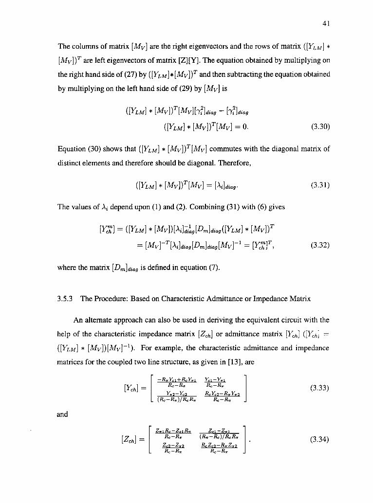
35 DERIVATIONS amp PROOFS 39
351 Admittance Matrix n Coupled Lines 2n-Port System 40352 Proof [Kri] is Symmetric 40353 The Procedure Based on Characteristic Admittance or
Impedance Matrix 41
36 COMMENTS 43
4 MODELING AND CHARACTERIZATION OF MULTIPLE COU-PLED LINES FROM MEASUREMENTS 44
41 INTRODUCTION 44
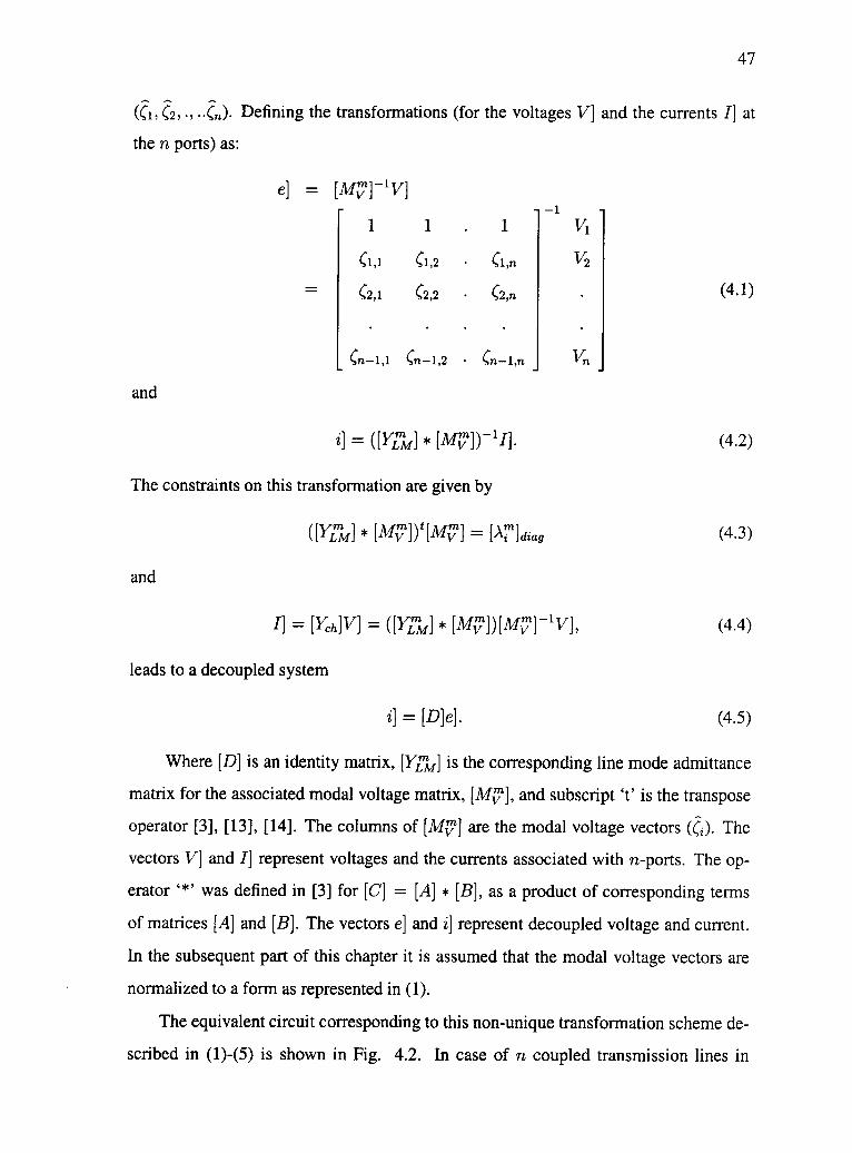
42 DECOMPOSITION PROCEDURE FOR CHARACTERISTICADMITTA-NCE MATRIX 46
43 DISCRETE TRANSITION MATRIX FUNCTION FOR UMCL 51
431 Input Impulse Admittance Matrix (LIAM) Function 53432 Measured Impulse Reflection Response (IRR) Matrix Func-
tion 55433 The Higher Order Terms 56
44 UMCL SYNTHESIS PROCEDURE 2n-Port System 57
45 RICCATI MATRIX EQUATION for UMCL 2n-Port System 60
46 EXAMPLE UMCL Three Lines System 61
47 DERIVATIONS amp PROOFS 66
471 Matrix [PT] is Di agonalizable 66472 Matrix [Ai]diag [pT] is Symmetric 67473 Inner Product 68474 Procedure Test for Completeness 68475 Necessary and Sufficient Conditions To Identify Normal-
Mode Parameters 70
48 COMMENTS 71
TABLE OF CONTENTS (CONTINUED)
Page
5 ANALYSIS OF MULTILAYER MULTILEVEL MIS TRANSMIS-SION LINE STRUCTURE 72
51 INTRODUCTION 72
52 FORMULATION 73
53 THE DIAGONALIZATION PROCEDURE 76
531 Single Level Metallization 76532 Multilevel Metallization 78
54 RESULTS 79
541 Line Parameters of a MIS Microstrip Line Structure 79542 Line Parameters of a MIS Based Strip line Structure 85543 Line Parameters of a MIS Based Coupled Microstrip Line
Structure 86
55 COMMENTS 90
6 CONCLUSION AND FUTURE WORK 91
BIBLIOGRAPHY 94
LIST OF FIGURES
Figure Page
11 A typical multilayer multilevel interconnect structure 4
21 A general MTLs system and the corresponding 2n-port MTL system 7
22 Equivalent circuit of coupled transmission lines in a homoge-neous medium based on [1] and [2] 11
23 Equivalent circuit of multiconductor transmission lines based on modal decomposition [3] [My] is the modal voltage eigenvec-tor matrix are the corresponding model characteristic impedances and Oi are the associated modal delays 11
24 Equivalent circuit of coupled transmission lines in an inhomo-geneous media based on the configuration-oriented model [4] Here the uncoupled transmission lines in the 7r and c part are of different electrical lengths 14
25 A typical die cross-section of MIS (Si Si02) structure 18
31 SPICE model for asymmetric coupled lines based on a four port admittance matrix (b) SPICE model based on four port impedance matrix Tc and 777 are the time delays associated with the c and 7r modes In case of lossy coupled lines the delays and the characteristic admittances of uncoupled transmission lines are function of frequency 26
32 SPICE model for symmetrical coupled lines based on a four port admittance matrix (b) SPICE model based on four port impedance matrix t-even and toad are the time delays associated with the even and odd mode In case of lossy coupled lines the delays and the characteristic admittances of uncoupled transmis-sion lines are function of frequency 27
33 Step response of the symmetric lossless coupled microstrip four port 34
34 Time-domain step response of the symmetric coupled microstrip four port on FR-4 substrate 34
35 Time-domain response of the asymmetric lossless coupled mi-crostrip four port 36
LIST OF FIGURES (CONTINUED) Figure Page
36 Frequency response of a two-section asymmetric coupled mi-crostrip filter on alumina for different dielectric losses (tan 5=
nitude of S21 in dB (c) Phase response of S21 Er =98 wl =0400002 and tan 5= 0042) (a) Magnitude of Sll in dB (b) Mag-
mm w2=025 mm s1=004 mm h=063 mm L=375 mm 38
37 Step response of the lossless three symmetric coupled microstripsix ports 39
41 A general lossless uniform multiconductor coupled lines (UMCL)2n-port system 45
42 Equivalent circuit corresponding to the voltage and current trans-formation 48
43 Equivalent circuit corresponding to the definition of partial modeadmittance matrix [M The internal resistance of the voltagesources in this figure are assumed to be zero 49
44 Microstrip structure uniform coupled asymmetric three lines 61
45 Measured reflected voltage response of a uniform coupled asym-metric three lines shown in Fig44 due to the step excitation(excitation voltage 05V) 62
46 The HAM step-response waveform (E3=0[7] 6 (t tj)) vs timeobtained from the measured reflected voltage response shown inFig 4 5 62
51 A general multilayer multilevel transmission line structure Herethe transmission lines are embedded in the lossy dielectric lay-ers 73
52 The network analog equivalent corresponding to Laplace poten-tial equation (b) The network analog equivalent correspondingto magnetic vector potential equation given by (7) 75
53 The discrete network analog and the algebraically equivalenttransformed network after diagonalization 77
54 Line impedance parameter Z(w) (= R(w) + jwL(w)) as a func-tion of loss tangent of lower substrate tanoi (a2 = 0) 80
55 Line admittance parameter Y(w) (= G(w) + jwC(w)) as a func-tion of loss tangent of lower substrate tan8i (o-2 = 0) 80
LIST OF FIGURES (CONTINUED)
Figure Page
56 ereff and ad as a function of loss tangent of the lower substratetan(51 (a2 = 0) 81
57 Characteristic impedance of the line as a function of loss tangentof the lower substrate tanoi (a2 = 0) 81
58 A typical MIS based coplanar stripline structure (h1 = lOpmh2 = 200pm w1 = 10pm w2 = 20ttm s = 10um fo = 10Er1 = 39 Er2 = 97 ao = 0 ii = 0) 82
59 The inductive and the resistive transmission line parameters as afunction of frequency for different conductivity a2 of the lowerSi substrate layer of the structure shown in Fig 58 83
510 A typical MIS based broad-side stripline structure (b) The in-ductive and the resistive transmission line parameters as a func-tion of frequency for different conductivity a3 of the lowerSi substrate layer (h1 = lOpm h2 = 10pm h3 = 200pmwi = 20pm w2 = 10pm s = 3pm 13 = 10 71 = 39Er2 = 39 Er3 = 97 ao = 0 al = 0 a2 = 0) 84
511 A typical MIS based coplanar coupled microstrip line structure(h1 = 10pm h2 = 200pm w1 = lOpm w2 = 20pm s =10pm f ro = 10 Eri = 39 Er2 = 97 ao = 0 a1 = 0) 86
512 The inductive and the resistive transmission line matrix param-eters as a function of frequency for different conductivity a2 ofthe lower Si substrate layer of the structure shown in Fig 511 87
513 A typical MIS based broad-side coupled microstrip line struc-ture (h1 = 10pm h2 = 10pm h3 = 200pm wi = 20pmW2 = 10771 s = 327n fro = 10 cri = 39 Er2 = 39Er3 = 97 ao = 0 a1 = 0 a2 = 0) 88
514 The inductive and the resistive transmission line matrix param-eters as a function of frequency for different conductivity a2 ofthe lower Si substrate layer of the structure shown in Fig 513 89
LIST OF TABLES
Table Page
1 IRR function zero and the first-order terms 63
2 HAM function zero and the first-order terms 64
3 Linear equations for evaluating the modal delays 71a nb and ne 66
Modeling and Characterization of Multiple Coupled Lines
Chapter 1
INTRODUCTION
For the last several decades modeling and characterization techniques for multi-
conductor transmission line (MTL) system have been a topic of active research Appli-
cation of this research in general includes several important fields of electrical engi-
neering One of the prominent applications of MTL system is in power systems for effi-
cient transmission of electrical energy from one point to another as in case of twomulti-
conductor power line Multilevel interconnects present on the multilayer printed cir-
cuit boards (PCBs) and in high-speed digital and high-frequency RF integrated circuits
are also examples of nonuniform MTLs MTLs also have several useful applications in
the area of microwave engineering especially in MM1Cs (Monolithic Microwave In-
tegrated Circuits) where they are widely used as basic building block element in some
of the passive structures [5] [6] [7] Furthermore in the field of signal processing and
system identification the propagation and electrical characteristics of MTLs can also
be indirectly linked with the development of several now widely used algorithms The
well established theory of design of lattice filters [8] [9] (digital filters) pertaining to
signal processing can be interpreted in terms of propagation and electrical characteris-
tics of transmission lines Another example is in the solution (eg single and multi-
dimensional peeling algorithm [10] [11]) of several problems explicitly classified as
single or multi-dimension inverse problems in the present system identification litera-
ture [8] [9] [12]
Several CAD-oriented (Computer-Aided-Design) models for application specific
MTLs based systems have been proposed and investigated in the past In general most
of these MTLs based systems have different CAD-oriented equivalent circuit models
for modeling their electrical characteristics despite the fact that all of these systems can
be described by the identical governing differential equations such as the transmission
2
line equations The same holds true for the electrical characterization techniques asso-
ciated with these application specific equivalent circuit models of MTL systems The
dependence of CAD-oriented equivalent circuit models and similarly the corresponding
characterization techniques are due to the exploitation or emphasis of different aspects
of the electromagnetic boundary value problems associated with these different appli-
cation This results in different frequency time and spatial variations in the correspond-
ing line parameters of the transmission line equations For example recent spectacular
advances in the processing technology of semiconductors has lead to the reduction of
active device sizes on digital and RF integrated circuits The reduction of the device
sizes such as MOSFET and BJT has made the associated parasitics smaller resulting in
significant improvement in switching speed and the high frequency analog operational
capabilities Furthermore demands of inclusion of more functionalities on die or on the
same board for better cost effectiveness has lead to the increase in density and elec-
trical lengths of interconnects used in connecting the high-speed circuit devices These
interconnects now occupy a major area (real-state) of the die in a modern day inte-
grated circuit The electrical characteristics of these high performance interconnects are
influenced by several factors which includes spatial variation of the interconnect metal-
lization inhomogeneity of dielectric layers conductor and dielectric losses and various
discontinuities such as vias steps and bends
The high speed interconnects are designed with the objective to maintain the sig-
nal integrity and the timing constraints (noise margins and timing budgets) at very high
frequency Thereby interconnects performance can significantly get affected by the
high frequency electromagnetic issues associated with these structures Unlike inter-
connects in power transmission lines EMC and the non-ideal ground effects (due to the
earth) are of significance and here the main emphasis is on the reduction of transmission
losses In such systems low frequency electromagnetic issues are more important and
the transmission lines are uniform or can have spatial variation along the direction of
propagation High frequency effects (on the corresponding MTLs line parameters) are
more dominant in applications involving usage of coupled transmission lines as passive
components in MMICs Here the MTLs are uniform or sometimes have spatial varia-
3
tion along the direction of the propagation In all of the above mentioned applications
MTL systems are designed to reduce all type of losses which include the radiation loss
(to reduce EMC related effects) In contrast to these applications in antenna systems
(eg dipole microstrip antenna etc) which can be considered as a transmission line
systems the objective is to enhance and modify the radiation pattern From the above
discussion it is apparent that different dominant effects as well as system specifications
for different applications determines the equivalent circuit CAD models as well as the
characterization techniques linked with the MTLs based system to only specific sets of
applications
11 OVERVIEW OF THESIS
In this thesis fundamental theory of coupled transmission line is revisited and some
new and significant results applicable to general MTL system are illustrated These re-
sults further reinforce the validity and importance of already existing formulation based
on the normal-mode parameters [13] [14][15] The presented work broadly addresses
the following key areas
An overview of current state of art in the modeling techniques for MTL systems
in microwave and high-speed interconnect applications
A new equivalent circuit CAD model (configuration-oriented model [2] [4]) for
uniform MTL system based on the single transmission lines
Relationship of this model (configuration-oriented model) with respect to already
existing equivalent circuit models for MTL system
Synthesis technique for a uniform lossless non-dispersive MTL system from the
measured time-domain reflection response
A quasi-TEM based network analog approach for extraction of line parameters of
MIS (Metal-Insulator-Semiconductor substrate) based multilayer multilevel trans-
mission line structures
4
Microstrip lines
Embededmicrostrip lines
Power planes
Strip lines
Figure 11 A typical multilayer multilevel interconnect structure
The presented results are useful in modeling and characterization of typical uniform
multiconductor transmission line structures in a multilayer dielectric and multilevel
metallization type of interconnect environment typically encountered on integrated cir-
cuits or in high performance digital RF or mixed signal printed-circuit boards Such a
schematic of a typical multilayer multilevel interconnect structure is shown in Fig 11
12 THESIS ORGANIZATION
A general review of MTLs from the historical perspective for modeling char-
acterization synthesis and the extraction of characteristics parameters by electromag-
netic simulation is presented in Chapter-2 In Chapter-3 a new CAD-oriented model
is proposed for the MTLs This model consists of a system of transmission lines and
has simpler SPICE input data requirements as compared to the modal decomposition
based models It is shown that this configuration-oriented model can in general be
implemented for the simulation of lossy and dispersive multiconductor inhomogeneous
5
structures The derivation of the circuit model is based on decomposition of the ad-
mittance or impedance matrix of the n coupled lines 2n-port system Closed form ex-
pressions for the model parameters for the important cases of asymmetric coupled lines
and symmetrical three coupled line structures are included in this chapter Time- and
frequency-domain simulation results for typical structures are presented to demonstrate
the applications of the configuration-oriented SPICE models
The problem of synthesis of an equivalent 2n-port system (for n uniform coupled
lines) from the reflection response of a uniform MTL system is a subset of classical
problems defined as multi-dimensional inverse problems In Chapter-4 a synthesis pro-
cedure for equivalent 2n-port system associated with n coupled lossless non-dispersive
transmission lines from the measured reflection response of a uniform MTL system is
proposed An entirely new transition matrix function of a uniform MTL system in the
discrete Fourier transform domain (z-domain) is derived The relationship between the
measured reflection response and the normal-mode parameters of MTL system are stud-
ied Later equivalence between the solution of special class of polynomial algebraic
Riccati matrix equation [120] and the synthesis procedure proposed in this chapter is il-
lustrated Furthermore to exemplify this procedure coupled three microstrip line 6-port
system is synthesized from the measured time-domain reflection response
In Chapter-5 a new approach based on network analog approach is proposed for ex-
traction of frequency dependent transmission line parameters of a MIS transmission line
structure This formulation is based on the vector magnetic potential equation applicable
to MIS structure A detailed description of how the magnetic potential equation can be
discretized and various boundary conditions implemented for a MIS transmission line
structures is illustrated The proposed approach is then applied to several useful MIS
transmission line structures to demonstrate the validity and accuracy of the approach
Conclusions and recommendations for possible future work based on the work re-
ported in this thesis are summarized in Chapter-6
6
Chapter 2 INTRODUCTION TO MULTIPLE COUPLED LINES
The analysis and modeling of coupled transmission systems including multicon-
ductor transmission lines has been a topic of considerable interest in recent years Ad-
vances in planar and layered interconnect and propagation structures and components
in microwave high speed digital and mixed signal circuits have resulted in increased
interest in efficient accurate analysis and design of these circuits and systems In this
chapter a general discussion of the coupled transmission line formulation and some
typical applications of coupled transmission lines in MMECs is presented The various
CAD-oriented models proposed for MTL systems in the current literature relevant to
the usage of MTLs as interconnects and passive components on integrated circuits or on
printed-circuit boards are summarized An overview of existing techniques for the syn-
thesis of transmission lines from the measured reflection and transmission response data
are reported Additionally a brief description of the techniques currently available for
the extraction of transmission line parameters of a multilayer transmission line structure
with special emphasis to MIS transmission line structures are discussed
21 COUPLED TRANSMISSION LINE FORMULATION
A general (n+1) multiconductor line system including the reference conductor
plane is shown in Fig 21 Assuming the given multiconductor transmission lines are
uniform along the length and the propagation modes are quasi-TEM the electrical char-
acteristics of this system are described by matrix telegraphers equations (or coupled
transmission line equations) as
av] az GR(w)] + jw[L(w)])ii (21)
aii az ([G(w)] + jw[C(w)])v] (22)
7
n
4 3
1 2 k vk (n-4-1)
a)
z
b)
Figure 21 A general MTLs system and the corresponding 2n-port MTL system
Here the kth element of vectors v] represents the voltage between the kth conductor
and the reference conductor Similarly the kth element of vector i] represents the cur-
rent flowing on the kth conductor The matrices [R(w)] [G(w)] [L(w)] and [C(w)]
are in general frequency dependent resistance conductance inductance and capacitance
matrices respectively corresponding to the given multiconductor coupled line system
From the circuit point of view the From the circuit point of view desired form of so-
lution for (1) and (2) is to describe the given n uniform multiconductor transmission
line system in terms of 2n-port (algebraic) system which is independent of the boundary
conditions associated with the transmission line equations This leads to an equivalent
2n-port circuit block element general enough to allow any terminal conditions in terms
of linear as well as nonlinear circuit elements at the ports The procedure for extraction
of 2n-port algebraic system corresponding to the partial differential equations given in
(1) and (2) is carried out by assuming e3wt-72 variation along the direction of propaga-
tion This assumption partially decouples the coupled transmission line equations The
resulting equations are further transformed by using linear transformations and leads
to a generalized matrix eigenvalue problem and the corresponding decoupled transmis-
sion line equations The solution of the generalized matrix eigenvalue problem and the
8
associated decoupled transmission line equations can be described in terms of 2n-port
algebraic system Moreover this 2n-port system can be expressed in terms of well know
2n-port impedance admittance ABCD or the scattering matrix parameters [13] [14]
[15]
In general the circuit simulation and design of these structures is normally based on
the characteristic parameters derived from a rigorous frequency dependent electromag-
netic solution or the line constants derived from quasi-static solutions The quasi-static
solutions lead to the [R] [L] [G] and [C] matrices associated with the multiconduc-
tor system The frequency dependent full wave solutions lead to the computation of
eigenvalues eigenvectors and eigenfunctions from which equivalent frequency depen-
dent elements of the [R][L][G] and [C] matrices can also be calculated Discussion
of capacitance and inductance matrices in terms of modal power is presented in [16]
Similarly in [17] the quasi-TEM analysis of lossless coupled transmission line system
in an inhomogeneous medium is reviewed Starting from the generalized telegraphers
equations the characteristic impedance of the normal-mode parameters using power-
current power-voltage and voltage-current is defined and computed Some examples of
quasi-static and full wave approach based on one of these definition can be found in [3]
[15] [18] [19] Despite availability of procedure for representing coupled transmission
line equations as a 2n-port system in terms of normal-mode parameters survey of re-
cent literature reveals several different formulations [20] Many of the formulations can
lead to nonphysical values for the normal-mode parameters associated with the 2n-port
system and was explicitly demonstrated in [21] The details of the procedure for rep-
resenting coupled transmission line system in terms of 2n-port system and the physical
significance of normal-mode parameters are reported in [3] [4] [13] [14] [15]
22 SOME APPLICATIONS OF MULTIPLE COUPLED LINES
As alluded earlier interconnects are composed of nonuniform MTLs and therefore
MTLs are the essential components of integrated circuits and the printed-circuit boards
for connecting various active devices Also in case of microwave integrated circuits
9
MTLs are also used in the design of passive devices Despite several advancement
in the design and wide usage of these passive (devices) structures several issues still
remain unresolved and are at present subject of ongoing research Here some of the
typical recent advances in the applications of MTLs in various passive structures are
briefly reviewed
Application of coupled line in the design of couplers have been widely investigated
and reported in the literature Design procedure for asymmetric couplers (based on
coupled transmission line) with equal phase velocity have been derived in [22] Gun-
ton in [23] has derived design equations for the S-parameters for 4-port couplers with
non-mode converting impedances based on the formulation for inhomogeneous coupled
transmission lines given by Tripathi [13] A more general formulation based on the
optimization has been reported by Chin [24] for the design of couplers with real ter-
mination impedances Sellberg [25] derived explicit formulas for the synthesis and the
optimization of general uniform contra-directional couplers having complex termination
impedances Thereby the known method of compensating different phase velocities (c
and it modes) using shunt capacitors can now also be included in the design procedure
using this formulation Couplers based on coupled dielectric waveguide microstrips
and coupled finline structure with co-directional orand contra-directional coupling has
been reported in [5] [6] [22] [23] [26] [27] [28] Except for some special cases a
general solution to the problem of synthesis of asymmetric coupled line coupler remains
unresolved and is an area of active research
In [29] [30] [31] a design procedure for edge-coupled transmission line transform-
ers for designing networks to provide DC isolation for biasing active circuits in MMIC
applications has been reported Quirarte has in [7] demonstrated how different config-
urations of coupled lines or parallel connected coupled lines can be used together to
obtain differential phase shifters Yansheng has shown that several short sections of two
or more coupled lines when alternatively connected together can achieve the needed per-
formance of a single-section coupler and phase shifter [32] This analysis is restricted to
symmetrical structures Applications and design procedures for filters based on special
cases of MTLs are described in [33] [34] [35]
10
In recent years design procedures for the reduction of crosstalk for coupled inter-
connects is also being actively investigated Use of substrate compensation to control
crosstalk and coupling was reported in [36] A layout technique which reduces the near-
est neighbor crosstalk for multiconductor signal buses is presented in [37] A technique
to analyze two conductor transmission lines with rectangular notch in the dielectric layer
between the two strip for reduction of the crosstalk is presented in [38] In general much
of the work reported regarding application of MTLs as circuit elements concerns only
with few special cases of a general MTLs system Application of general normal-mode
formulation [13] [14] to various MTLs based devices is still a subject of active research
23 CAD-ORIENTED MODELING TECHNIQUES
Computer-Aided-Design (CAD) methodologies for the design simulation and op-
timization of integrated circuits are presently an integral part of integrated circuit design
cycle Sophisticated and accurate SPICE models for basic circuit elements or device
model libraries are essential elements for a successful design MTLs as interconnects
or passive devices are now important structures and can significantly affect the perfor-
mance of integrated circuits Crosstalk noise due to reflections skews absolute delays
and ground bounce limits the performance of digital and RFICs and have now become
important issues to be included in the design cycle Thereby accurate and computa-
tionally efficient CAD models of MTLs are essential and are at present an active area
of research CAD models based on the equivalent circuits (model is generated using
existing SPICE elements) and transfer function based techniques are the two distinct
ways addressed in the current literature for modeling the MTLs based systems We
here review the current state of art in the modeling techniques for MTLs and also their
evolution with time Modeling techniques for MTLs from the perspective of intercon-
nects modeling and passive structures modeling in microwave and RF systems are only
considered
11
symmetric coupled lines
single transmission line
single transmission line
Figure 22 Equivalent circuit of coupled transmission lines in a homogeneous medium based on [1] and [2]
tylv(11) I Mv(1i) I
Mv(11) e Mv(11) e
112
13
61 NAV(3i) Mv(30 I
Em11 Mv(3i) e MY(31) e er
Imv(li) mv(ni)
e Mv(ni) e
Figure 23 Equivalent circuit of multiconductor transmission lines based on modal de-composition [3] [Mv] is the modal voltage eigenvector matrix are the corresponding model characteristic impedances and 92 are the associated modal delays
12
231 Equivalent Circuit Models
Several circuit models based on the solution of coupled transmission line equations
have been proposed in the past For a lossless multiconductor transmission line structure
in a homogeneous media Seviora [39] presented an n coupled transmission line equiva-
lent circuit which requires only single transmission lines Approximate synthesis proce-
dures for a 2n-port admittance matrix associated with coupled transmission lines using
transmission lines and short-circuit stubs was reported in [40] [41] These methods had
negative characteristic immittance in the equivalent circuit Equivalent circuit based on
a pair of non-symmetrical coupled lines where the coupling between the neighboring
lines were taken into the account was reported by Grayzel [42] A general equivalent
circuit for n coupled lines in homogeneous media based on the generalization of [42]
was presented in [1] An example of such an equivalent circuit for the case of coupled
transmission line system is shown in Fig 22 The basic element of this equivalent cir-
cuit consists of symmetrical coupled lines and transmission lines to model a general n
coupled transmission line structure excluding the reference conductor The number of
elements needed in the equivalent circuit is at most (n2 n + 2)2 For the case of loss-
less coupled transmission lines in inhomogeneous media with frequency-independent
line constants a SPICE model based on modal decompositions was proposed in [19]
This model represents the congruent transformer bank [43] by dependent sources and
leads to a circuit model consisting of linear dependent sources and ideal delay elements
representing uncoupled transmission lines (ref Fig 23) This model was also extended
to lossy MTL system in [19] The disadvantage of this model is that the linear dependent
source elements vary with frequency This means that the model is not appropriate for
the transient analysis usually performed on time- domain circuit simulators
Simplified versions of the model valid for special cases of homogeneous electri-
cally identical lines with near neighbor coupling only have also been reported [44] [45]
A rigorous procedure leading to the configuration-oriented equivalent circuit model
consisting of a system of transmission lines only was reported for the case of homoge-
neous media in [2] (ref Fig 22) The number of transmission lines elements needed in
13
the equivalent circuit is at most n(n+ 1)2 Similar useful models valid for special cases
of inhomogeneous structures have also been proposed and used in the design of coupled
lines circuits [34] [46] [47] [48] [49] These models are not suitable for a general
multiconductor transmission line structure A general configuration-oriented equivalent
circuit model for multiconductor transmission lines in an inhomogeneous medium is
reported in [4] (ref Fig 24) This circuit model demonstrates that the multiconduc-
tor coupled line system can be represented in terms of uncoupled transmission lines
These uncoupled transmission lines are connected in a configuration-oriented fashion
The number of transmission line elements needed in the equivalent circuit is at most
n2(n + 1)2 Modeling of lossy and lossless uncoupled transmission lines in this cir-
cuit model can be performed via several widely available and reported CAD oriented
models for single transmission line system in the present literature For example with
configuration-oriented model a very useful and most commonly used algorithm for tran-
sient analysis of lossless transmission line system based on the method of characteristics
proposed in [50] can be used in the simulation of lossless uncoupled transmission lines
The method of characteristics has been also extended to lossy transmission lines system
in [51] [52] Here the transfer function of lossy line is approximated in terms of lumped
and distributed circuit elements which again can be used for simulating the lossy uncou-
pled transmission lines present in the configuration-oriented equivalent circuit model
232 Alternate Modeling Techniques for MTLs
As an alternative to the equivalent circuit methods where the emphasis is on ob-
taining the equivalent circuit of MTLs with the already existing SPICE circuit elements
several modeling techniques for MTLs which needs some preprocessing before SPICE
implementation has been proposed in the current literature In this section some of
these alternative methods are reviewed
Approximating transmission lines in terms of simplified pole-zero description has
been investigated in [53] [54] In [55] a distributed interconnect model is proposed for
14
configuration-oriented model for it mode
single transmission line
single transmission line
single transmission line
single transmission line
single transmission line
single transmission line
configuration-oriented model for c mode
Figure 24 Equivalent circuit of coupled transmission lines in an inhomogeneous media based on the configuration-oriented model [4] Here the uncoupled transmission lines in the 7r and c part are of different electrical lengths
a self-damped lossy transmission lines A method for transient analysis of lossy trans-
mission lines with an arbitrary nonlinear terminal networks is presented in [56] [57]
Here the time-domain Green function is evaluated for the multiconductor transmission
lines by terminating the ports with the quasi-match loads to ensure short duration of
Green function response A procedure based on the method of characteristic for simu-
lating lossless coupled line was demonstrated by Chang [43] and later extended to mul-
ticonductor lossy coupled transmission lines structure by Orhanovic and Chang [58]
[59] [60] A new approach for the time-domain simulation of transient on a dispersive
and lossy coupled transmission lines terminated with the active devices was reported in
[61] [62] This method combines scattering matrix of an arbitrary line and the nonlinear
causal impedance functions at load ends to derive expressions for the signals at the near
and the far end Numerical inversion of Laplace transform has been an important tool for
time-domain analysis of high speed VLSI interconnects modeled by transmission line
network A procedure based on inversion of Laplace transform is presented for analysis
15
of lossy coupled transmission lines with arbitrary linear termination and interconnect-
ing network is proposed in [63] [64] Methods based on this procedure leads to slow
decaying functions during Laplace inversion and therefore the convergence of inversion
procedure in [63] [64] can be computationally inefficient
For a nonuniform MTL systems also several CAD oriented modeling techniques
have been proposed in the literature In [65] time-domain scattering parameters of
MTLs are formulated and the nonuniform section is modeled by cascaded uniform sec-
tions for simulating nonuniform MTL system This procedure can lead to a very large
number of cascaded uniform sections making the approach computationally inefficient
A procedure based on asymptotic waveform evaluation (AWE) technique is reported
in [66] [67] [68] In this procedure Pades moment-matching methods are used to
approximate the frequency-domain transfer function of linear circuit by an equivalent
circuit with fewer number of poles and residues The disadvantage of this method is
that the moment matching is done at the single point and leads to fewer number of
poles This is due to the ill conditioning of the Hankel matrix resulted in the solution
of unknown terms in the equivalent circuit Multi-point moment matching techniques
such as Complex-Frequency-Hopping (CFH) or multi-point Pades approximation [69]
has been suggested as an alternative to AWE For a lossy coupled line system moment
matching with Pade and CFH has been applied to obtain dominant poles of an equivalent
network for frequency- and time-domain simulation is illustrated in [70] This approach
can be computationally inefficient and requires multiple expansions To model transient
response of nonuniform coupled line system a method of convolution-characteristics is
reported in [71] Based on Chebyshev expansion for the spatial variations of line pa-
rameters in transmission line equations a all purpose multiconductor transmission line
model is described in [72] [73] [74] for efficient and robust interconnect simulation
using a nonlinear circuit simulator such as SPICE
In general most of these alternative approach are based on the theory of approxi-
mations and are ideal for nonuniform coupled transmission line interconnects structures
The disadvantage of some of these methods is that they are unsuitable for the broad
range of interconnects typically encountered in different substrate environment Some
16
discussion where the need for an alternative approach especially based on the equivalent
circuit model approximation have been discussed in [75] [76] Additionally many of
the alternative approaches sometimes can lead to an equivalent transfer function which
violates some of the inherent properties related to physical systems such as symmetry
and energy conservation present in the coupled transmission line equations This results
in unstable or physically unrealizable MTLs transfer functions
24 SYNTHESIS TECHNIQUES
Synthesis techniques of a nonuniform transmission line system based on the in-
verse scattering (based on linear equations layer-adjoining approach and its dual the
Schur-type algorithms layer-peeling algorithm) has fascinated both the engineering
and mathematical community alike This is due to the linkage of these techniques to
the solution of some of the very complex engineering problems In general the syn-
thesis techniques for lossless nonuniform transmission line system classified as one-
dimension inverse problem are now well established and are routinely and extensively
used for many diverse applications Some examples of these applications include inter-
connect modeling [10] [11] in signal processing for modeling of vocal tract for speech
synthesis in image processing and non-destructive testing for biomedical and material
science applications A brief overview of some of the significant historical contributions
in the synthesis methods of transmission lines based on the inverse scattering techniques
is presented here
In [77] using a discrete inverse scattering technique impedance-profile of a nonuni-
form transmission line is synthesized which reflects an arbitrary waveform Youla [78]
and Wohlers [79] developed the realizability and uniqueness proofs for uniform trans-
mission lines with resistive and inductive terminations in frequency-domain A synthe-
sis procedure for a tapered line has been proposed in [80] Gopinath [81] presented
a treatise on the existence and uniqueness of nonuniform transmission lines in time-
domain with the constraints on the propagation velocity to be constant Orlov [82]
developed the theory for nonuniform lines of arbitrary impedance profile A detail de-
17
scription of theory reported in [82] and several other practical inversion and synthesis
techniques is provided by Bruckstein [8] [9] In this paper relationships between the
layer-peeling algorithm and layer-adjoining algorithms proposed for solutions of one-
dimensional inverse scattering problems are illustrated An approximate synthesis pro-
cedure for a lossy nonuniform transmission line system from the measured time-domain
reflection and transmission data has been proposed in [83] Unlike lossless case a gen-
eral solution to the problem of synthesis of lossy nonuniform transmission line still
remains unresolved
The synthesis techniques developed for a single nonuniform transmission lines have
been also extended to several useful special cases such as coupled symmetric transmis-
sion lines and the multiconductor coupled lines in a homogeneous media [10] [11]
[84] In case of coupled line system an optimization based approach is proposed in
[85] for modeling the board-level and package-level interconnect circuitry based on the
measured time-domain reflectometry data In [86] an experimental technique based on
principle of causality has been proposed for circuit modeling and synthesis of multicon-
ductor transmission lines In this paper only symmetrical coupled line structure is used
as a test vehicle to demonstrate the approach which can be easily reduced to a problem
of synthesis of single line using the constraint of symmetry An approximate design pro-
cedure for the planar microwave filters based on theory of inverse scattering has been
proposed in [87]
Approximate characterization techniques both in the frequency- and time-domain
for a general lossless uniform MTL system from the measured reflection (and transmis-
sion) data using optimization have been proposed with a limited success [88] [89] In
[90] a general synthesis procedure for lossless uniform MTL system from the measured
reflection data is proposed Here the necessary and sufficiency conditions for the extrac-
tion of all the normal-mode parameters of uniform multiconductor transmission lines
from the measured reflection data are derived [90] A lossless uniform MTL 2n-port
system terminated in a resistive network is only considered A general solution to the
problem of synthesis of losslesslossy nonuniform MTL system which can be classified
as multi-dimensional inverse problem still remains unresolved
18
Microstrip linesEmbeded microstrip line
l lummumer1111111111111111111111
Powerplanes
Conductor CO3 Si-02
1111111111111111111110111111111 reg Si
Figure 25 A typical die cross-section of MIS (Si Si02) structure
25 MODELING OF MULTILAYER TRANSMISSION LINES
Among the several some of the general criteria for the selection of a CAD-oriented
EM simulation tools for a particular application are
Accuracy and easy in implementation
Computational efficiency
Output parameter format (ie the extracted parameters of these tools should di-
rectly lead to the SPICE circuit elements which can then be easily incorporated in
the circuit design tools)
Range of validity (ie the extracted values should be valid over the wide range of
input parameters values)
Although several EM-simulators which use accurate full-wave techniques ([91]
[92] [93] [94] [95]) are available the EM simulation tools based on the quasi-static
19
approximations satisfy all of the above criteria for the present RF and digital applica-
tions Therefore the EM simulation tools based on the quasi-static techniques ([96]
[97] [98] [99] [100] [101] [102] [103] [104]) are widely preferred for modeling and
design of planar multilayer transmission lines or similar structures Examples of these
similar structures which are subset of general multilayer transmission line structure in-
cludes stripline microstrip line edge-coupled microstrip line and broad-side coupled
microstrip line
Accurate CAD-oriented electromagnetic (EM) simulation tools for the characteri-
zation of CMOS or GaAs multilayer MIS transmission lines structure are important for
the design of high speed digital and RFICs An example of a typical Si-SiO2 trans-
mission structure is illustrated in Fig 25 [105] The propagation characteristics of
such structures with lossy media depends on the conductivity of substrate layer In case
of single transmission line on a CMOS substrate (Si-SiO2) the propagating mode can
be classified as quasi-TEM slow-wave and the skin-effect mode This classification
is based on the propagation characteristics of the mode [106] Similarly for n cou-
pled lines in a multilevel Si-SiO2 structure (CMOS) the n propagating modes can also
be classified into the three mode categories as defined in case of single transmission
line [91] The modal characteristics of these n coupled transmission lines and hence
the distributed transmission line matrix parameters exhibit significant frequency depen-
dence In general the modes classified as the skin-effect modes are the dominant modes
of propagation for these transmission lines at the RF frequencies particularly for ICs
in CMOS technology The associated frequency dependent modal characteristics of this
mode can also be expressed in terms of frequency dependent distributed transmission
line parameters Quasi-static techniques proposed in [103] [104] [107] evaluate the
distributed inductance matrix by replacing the dielectric media by an air media and
then solving the Laplace equation associated with the corresponding boundary-value
problem Therefore in these implementations the effect of substrate current on the in-
ductance matrix of a multilayer MIS transmission lines structure with lossy substrates
are hence not included in the simulation The efficient quasi-static techniques in [100]
[108] which readily lead to the normal-mode parameters [13] required in the circuit
20
design of MTL system based interconnection and passive structures in the CMOS tech-
nology such as inductors and transformers are only limited to the quasi-TEM and the
slow-wave modes Several measurement based characterization techniques for the trans-
mission lines on Si-SiO2 substrate has been also investigated in [109] [110] to study
their propagation and the impedance characteristics Many new CAD models based on
optimization of the electrical response (limited to a particular structure) or based on
modification of existing closed form formulas for special cases of MIS transmission
line structures are proposed in [111] [112] [113] [114] In [115] the effect of substrate
current is included via a quasi-static formulation based on the magneto-static potential
equation Based on this formulation a CAD-oriented spiral model valid for quasi-TEM
slow-wave and skin-effect region is demonstrated in [116]
Several full-wave methods for evaluating the propagation characteristics of MIS
transmission lines structures have been also actively investigated Techniques based
on the hybrid methods have been also proposed for the characterization of multilayer
transmission line structure Some recent work in this direction is briefly reviewed here
The full-wave method based on Spectral-domain approach is an important technique
widely preferred for CAD based EM simulators (eg Momentum HP EEsoF) Some
of the main advantages of this approach are computationally efficient numerically sta-
bile and easy to implement In [91] [93] the full-wave Spectral-domain technique has
been applied to analyze MIS based microstrip line symmetric and asymmetric coupled
microstrip lines In these formulations the thickness of conductors are not taken into
the account which can significantly affect the electrical characteristics of MTL system
Furthermore it is only suitable for planar layered structures Hybrid mode formulations
which in general are combinations of two or more techniques have been proposed for
more practical interconnection structures In [94] lossy coplanar type transmission lines
are analyzed using a hybrid mode formulation based on the full-wave Spectral-domain
approach and the perturbation method Ching-Kuang [95] has proposed a full-wave
mixed potential based mode matching approach for the analysis of planar transmission
lines For homogeneous and inhomogeneous doping profile a hybrid mode analysis is
presented in [117] to characterize the propagation properties of uniplanar slow-wave
21
MIS coplanar transmission lines A rigorous procedure for evaluating the frequency de-
pendent propagation characteristics of lossless and lossy open coupled polygonal con-
ductor transmission lines which includes the case of thick conductors is presented [92]
Similarly Jun-Wu [118] has presented a full-wave technique for evaluating the prop-
agation and losses in a lossy line system A full-wave mode matching procedure for
analysis of planar transmission line structure is reported in [95] The full-wave methods
can accurately model the propagation characteristics of MIS transmission line structure
but are generally computationally inefficient and therefore not suitable for CAD imple-
mentation
26 COMMENTS
In this thesis multiconductor transmission lines are revisited with particular em-
phasis to address the present requirement of general CAD-oriented model and theoret-
ical framework for efficient transient analysis of uniform MTLs on time-domain simu-
lators A new CAD-oriented equivalent circuit model (configuration-oriented model) is
proposed which consists of single transmission lines Although several CAD models
had been already proposed in the past this model provides more physical insight into
the normal-mode theory proposed in [13] for coupled transmission lines It also includes
the case of lossy dispersive uniform MTL system The requirement of this model in bet-
ter understanding of normal-mode theory for the design of general asymmetric coupled
microstrip line filters was particularly alluded in [34] Equivalence between this model
[4] the model based on modal decomposition [3] and the normal-mode parameters [13]
[14] is illustrated Later using this equivalence a synthesis procedure for uniform MTL
2n-port system from the measured time-domain reflection response is reported [90]
Also a new approach based on the magneto-static potential equation and solved via
network analog approach is described for modeling multilayer multilevel layered MIS
transmission line structure
22
Chapter 3
A CONFIGURATION-ORIENTED SPICE MODEL
31 INTRODUCTION
In this chapter the configuration-oriented SPICE model for a general case of in-
homogeneous multilayer multiconductor lines is reported This model is an extension
of the earlier configuration-oriented model proposed in [20] for uniform MTL system
in a homogeneous media to a more general case of inhomogeneous media [4] The pro-
posed equivalent circuit model consists of uncoupled transmission lines connected in the
configuration-oriented fashion as was the case in the earlier model [20] A general for-
mulation and the extraction procedure for equivalent circuit based on the configuration-
oriented model for n multiconductor transmission line system is described This proce-
dure is based on the admittance matrix of 2n-port system associated with the n coupled
lines and leads to a configuration-oriented model based on the 7r-type of topology [4]
[119] A similar procedure based on the impedance matrix can also be derived and
leads to a configuration-oriented model based on the T-type of topology [4] [119] The
T-type of topology is the dual of 7r-type of topology [119] The procedure is then il-
lustrated by applying it to a case of general asymmetric coupled line Network models
based on the 7F and T type of configuration-oriented model topologies are demonstrated
and equivalence with the similar models proposed in past for special cases of coupled
lines is shown Another procedure for obtaining the configuration-oriented model based
on the decomposition of characteristic admittance matrix is exemplified by applying
it to a case of three symmetric coupled microstrip lines [14] The applicability of the
configuration-oriented model to a multiconductor lossy coupled line system is discussed
Several examples of typical applications of configuration-oriented models in microwave
and digital realms are presented to demonstrate the accuracy and the versatility of the
proposed equivalent circuit model This chapter includes the derivations and proofs of
the results used in the chapter
23
32 EQUIVALENT CIRCUIT MODEL
The configuration-oriented SPICE model consists of a network of uncoupled trans-
mission lines characterized by their propagation constants and impedances The model
can be readily derived from the admittance (impedance) matrix characterizing the 2n-
port system as described in this section
The procedure for deriving the expression for the admittance or impedance matrix
of the general 2n-port is well known and is based on the solution of coupled transmission
lines equations
av] (31)az
ai] (32)az
where vectors v] and i] represent voltages and currents on the lines and
[Z (w)] [R] + jw[L] [Y (w)] = [G] + jw[C]
[R] [L] [G] [C] are the per unit length line constant matrices whose elements are in
general frequency dependent The coupled transmission lines equations (1) and (2)
are decoupled with the help of voltage and corresponding current eigenvector matrices
[Mv] and [M1] = [My]-) respectively leading to the characterization of the
general n lines 2n-port by its admittance matrix [15] as given by (refer section-(351))
[YA] [YB] (33) [YB] [YA]
with
[YA] = [YLM] [My][Coth(7j1)]diag[MI]T
[YB] = [YLM] [MV][CSCh(7i1)]diag[MI]T
YLM11 YLM12 YLMln
[ YLM]nxn =
YLMn1 YLM nn
24
where -yi represents the ith eigenvalue and is the ith normal-mode propagation constant
[YLM] is the line mode admittance matrix whose element ILAI km represents the charac-
teristic admittance of the kth line for mth mode and is the length of the uniform coupled
multiconductor system The operator was defined in [15] for [C] = [A] [B] as a
product of corresponding terms of matrices [A] and [B] It is readily shown that the
admittance matrix of the 2n-port as given by equation (3) can be decomposed as
(34)[Y] E[Ym]m =1
The [Ym] represents the partial admittance matrix of the 2n-port corresponding to mode
m and can be expressed as
cotheym1)[Knh] cscheym1)[Yenh] [Ym]2nx2n (35)
csch(1mO[Yer1] coth(ym1)[Yg]
where
[Kinnxn = anm] [Mv])[Dm]diag[Mr]T (36)
and
Dm (j i) = 0 m [Dm]diag = (37)
Dm(j j) = 1 j = m The symmetric matrix [Yji ] (refer section-(352)) defined in equations (5) and (6)
corresponds to the characteristic admittance matrix for mode m and its (ij)th element
is given by
Yeri (i j) = YLM(i m)Mv (i 17)MT (m (38)
The matrix [Ym] in (5) is similar to the 2n-port admittance matrix corresponding to n
coupled lines in a homogeneous medium Recalling that the admittance matrix of a
transmission line two port having length 1 propagation constant -y and characteristic
admittance Y is given as
[ Y coth(71) 17 csch(-y1)
[112x2 (39) cschey1) coth(71)
25
Symmetry of [17h] implies that the 2n-port network represented by [Ym] consists of
these transmission lines connected in so-called configuration-oriented manner [2]
That is the partial admittance matrix [Ym] for mode m is synthesized by a homoge-
neous configuration-oriented model [2] having transmission lines electrical lengths cor-
responding to the mth mode eigenvalue The complete network then is obtained as a
parallel combination of the n 2n ports with each 2n-port corresponding to an orthog-
onal mode A similar procedure can be applied to the impedance matrix leading to a
dual topology and corresponding network of transmission lines that is equivalent to the
multiconductor multiport It is seen that the admittance or impedance matrix of a n
multiconductor transmission lines system can in general be simulated by n2 (n + 1) 2
transmission lines In the case of symmetry the number of lines are reduced depending
upon the type of symmetry
An alternate approach of deriving these circuits involves the use of the characteris-
tic impedance or admittance matrix of the coupled system These matrices represent a
network which terminates all the modes simultaneously on all the lines The elements
of these matrices represent the characteristic immittance of the transmission lines that
constitute the equivalent circuit The length of the transmission lines corresponds to the
electrical length of the corresponding mode Both the 2n-port and the characteristic im-
mittance matrix based decomposition procedures of course lead to the same equivalent
circuit representation (refer section-(353))
33 NETWORK MODEL FOR UNIFORM COUPLED LINES
The procedure presented in the previous section is applied to general asymmet-
ric and symmetric three lines cases to illustrate the technique and derive closed from
expressions for the modal parameters for these two important cases
26
1 0
20
Y1 17t TIC
Y1 1 c Tc
111 37C Tit
Y1 3c Tc
Y120 Tc
Y1 27c T7c
a)
zi 7c Tit
zi 1 c Tc
Z 2c Tc
Z Tit
Z1 3c Tc
Z1 37t Tit
b)
04
03
Figure 31 SPICE model for asymmetric coupled lines based on a four port admittance matrix (b) SPICE model based on four port impedance matrix 7 and T are the time delays associated with the c and 7r modes In case of lossy coupled lines the delays and the characteristic admittances of uncoupled transmission lines are function of frequency
27
a)
04ZOdd tOdd
Zodd todd20 03
-Zodd 2 todd
Zeven 2 teven
b)
Figure 32 SPICE model for symmetrical coupled lines based on a four port admittance matrix (b) SPICE model based on four port impedance matrix teven and todd are the time delays associated with the even and odd mode In case of lossy coupled lines the delays and the characteristic admittances of uncoupled transmission lines are function of frequency
28
331 Asymmetric Coupled Lines
A general uniform coupled two line system can be decoupled in terms of two
propagating modes it and c [13] The voltage and the corresponding current eigenvector
matrices [Mv] [M1] can be defined as ([13])
and [ R1e R1
Rir Rc[MI] = ([MV] 1)T (310)R 1
Re[ 1 1 1
Where y7 and 7 represent eigenvalues and are the normal-mode propagation constants
for the it and c modes 1 and Re represent the ratio of voltage on line two with respect
to line one for it and c modes respectively [13] The line mode admittance matrix [Km]
is expressed as
[ Ycl Yore [YLM]2X2 = (311)
Yc2 Yr2
The admittance matrix of the general asymmetric two line system [13] obtained from
equations (3)(10) and (11) is expressed as a sum of two matrices corresponding to the
two modes using equations (4)-(8) and are found to be
[coth(70[Vh] csch(71)[YA][Y]4x4 =
csch(70[Yel] coth(71)[Yelrh]
[coth(771)[Ycel] csch(71)[Ycch]+ (312)
csch(71)[17ch] coth(7cl)[Ycd c
where
RcY7r 1 -zIza_ Rc Rir Rc R-r
[Ycirld = [ 1712 RirKr2
(Rc Rm) I Rc Rir Rc Rir
RirKi yea_ and [YA] Rc RA Rc Rir= [ (313)K2 RcK2
(Rc Rir) I Rc Rir Rc Rir
29
Each matrix [Y] and [Y]c in equation (12) can be synthesized in general by three trans-
mission lines connected at the input and output ends in a 7 configuration [2] These
two networks connected in parallel yield a complete equivalent circuit as shown in Fig
32a for the coupled line system The expressions for the characteristic admittance of
the transmission lines in the SPICE model in Fig 32a correspond to the admittance
matrices given by equation (13) and are given by (see eqns (37) and (38))
yhlr Yid (Re 1) y217 RrYr 2(RRire 1) Re Rr
y317r Yci(1 R7r) 1771 RgtRcR
RcYc2(13721c = R-7r) Y31c (314)Re Rr
As noted earlier the impedance matrix can also be used to construct an alternate
equivalent model of the coupled system The impedance matrix of a general asymmetric
coupled line system given in [13] is readily decomposed into two modes
[44x4 = [Zr]4x4 + [Zd4 x 4 (315)
Each matrix in equation (15) can be modeled by three transmission lines connected in a
T configuration for each mode The complete equivalent circuit is shown in Fig 32b
The expressions for characteristic impedance of the transmission lines in this SPICE
model (Fig 32b) are given by
Zir Re Z712(1 R) = (1 R)
Re R ZwifteRZi = 3ir Hir(Rc )Re R
Z Z ReR Z 21c (316)
Re R (Rc 1) Rc
It should be noted that the characteristic impedance and admittance matrices of the cou-
pled lines system are symmetric and represent a passive n-port network However the
characteristic impedance of some transmission lines in the equivalent circuit can be
30
negative depending on modal decomposition The decomposition of the characteristic
admittance matrix (stable and passive network) into the sum of n partial admittance ma-
trices leads to a stable configuration-oriented model in spite of the fact that some of the
elements are not passive This is like having two equal length lines in parallel For a
stable system one of them can have negative characteristic admittance as long as the
total combined characteristic admittances of the two lines is positive These negative
impedance transmission lines can be simulated by a positive impedance transmission
line elements with the linear dependent sources for the impedance conversion or directly
as a negative impedance transmission lines on many CAD tools like LIBRA Further-
more in case of symmetric lossless coupled lines (ft = 1 Rc = 1 1771 = 17r2 and
Yci = K2 leads to Yodd=2Y31 and Kven=Yilc) the model reduces to the four transmis-
sion lines system presented in [47] (Fig 32a) or to the T equivalent network as shown
in Fig 32b (Zeven=24 and Zodd=ZL) Similarly for the case of lossless symmetric
coupled lines in a homogeneous medium (y = ye) the equivalent system reduces to a
three transmission lines system as in [2]
332 Symmetric Three-Coupled Lines
For the case of symmetric coupled three-line structures the voltage and associated
current eigenvector matrices corresponding to the three propagating modes a b and c
are given by [14]
1 1 1
[Mr] = 0 Rv1 Rv2 (317)
1 1 1
and
Rvl R2 Rvl [M1] = ([11117]-1)T 0 2 2 (318)2(Ri1 Ra)
Ru2 Rvl Rv2 Rvl
31
The line mode admittance matrix [Kw] is
Yal Ybl Ycl
[YLM]3x 3 = Ya 2 Yb2 Yc2 (319)
Ya3 Yb3 Yc3
and N -yb ye are the propagation constants associated with the normal-modes a b and
c [14] For three symmetric coupled lines Y- = Ya3 Yb1 = Yb3 and 17c1 = K3 Substi-
tuting equations (17)-(19) in equation (6) leads to the characteristic admittance matrices
for the modes ab and c and are given as (refer eqn (39))
Yal 2
0 2711
[Kahl = 0 0 0
Ya3 0 17-2 2
Ri2Ybi 2y 1
Rv1 Rv21762 2Rv1Yb2 Rv1Rv2n22(141 Rv2)
Rv2Yb3 2n3 Rv2Yb3
and
Rvl Ycl 2ic1 Rvl Ycl 1
[Kh] = Rv1Rv2Yc2 217b2Yc2 Rv1Rv2Yc2 (320)2(111 Rv2)
216Rvi Rvl Yc3
The six port transmission line network is then readily constructed as three modal
networks connected in parallel The complete network then consists of thirteen trans-
mission lines The expressions for the characteristic admittances for the lines are given
below (refer eqns (37) and (38))
Transmission lines between ports 1 and 4
Ybl (1 Rv2 ) Ycl (Rvl 1)
Rvi Rv2 Rvi Rv2
ports 2 and 5
32
ports 3 and 6
Rvi (1 Rv1
RE ) 142
YaRo (Rvi Rvi Rv2
1)
Yb3 (1
Rv1
terminal pairs (1 2) and (4 5)
Rv2) Rv2
(Ri1 1) pp
R-v2
Ycl
11 R2 R1 Rv2 terminal pairs (2 3) and (5 6)
Rv1Rv2162 Rv1Rv2K2 2(R1 Rv2) 2(Rv1 Rv2)
terminal pairs (1 3) and (5 6)
Yal Rv2Y61 RvlYcl 2 2(RA Rv2) 2(141 Rv2)
The electrical length of these transmission lines are given by the corresponding electrical
length of the three modes
333 Lossy Dispersive Multiconductor Coupled Lines
In general the coupled line systems have conductor and dielectric losses and
therefore the uncoupled transmission lines in the configuration-oriented model have
frequency dependent complex propagation constants and the complex characteristic
impedances The multiport SPICE simulation for lossy dispersive multiconductor cou-
pled lines can be accomplished by modeling the uncoupled lines obtained from the
formulation presented in section-(32) in terms of their two port frequency dependent
33
network functions such as [Y] or [S] parameters or modeling them in terms of equiva-
lent circuits consisting of ideal lumped and delay elements as shown in [52] for a single
microstrip The frequency dependent complex characteristic parameters (propagation
constants line mode impedances eigenvector matrices) are computed using a rigor-
ous frequency dependent technique like the Spectral-domain approach [15] or by using
CAD-oriented quasi-TEM methods (eg[121]) The model transmission line parame-
ters can be obtained in terms of equivalent frequency dependent self and mutual line
constants per unit length as shown in [122] As an example for the simple case of iden-
tical coupled lines the even and odd-mode propagation constants and impedances are
readily expressed as
= VRRplusmn Rm) + jw(Lplusmn
Lm)][(G Gm) + jw(C R Cm)] (321)
and
(R f R) + jcv(L f Lm)ZeO (322)
(G Gm) + jw(C Cm)
in terms of the frequency dependent equivalent line constants representing self and mu-
tual inductances capacitances resistances and conductances per unit length of the lines
For the case of low losses equations (21) and (22) can be simplified as
Ze0 (323)V CFCm
Yeo Lm)(C + Cm) +Rf Rm G
zie 0 (324)240 2
These line constants (R Rm L Lm G Gm C Cm) can be calculated by using quasi
static as well as full wave analysis of the coupled system [15] [121] [122] For the
general asymmetric coupled lines and multiconductor coupled systems the modeling of
individual lossy dispersive lines [52] in terms of network functions frequency depen-
dent line constants or equivalent circuits is similar to the symmetrical coupled line case
34
15 W1 w2
v1 Er
( v4
h
L
L 4I-0 3
v3
-05 0 5 10
T ps 15 20
Figure 33 Step response of the symmetric lossless coupled microstrip four port
15 wl s1 w2111-tan 8 -005
hEr vl
v4 1 0-1 I-0 42deg-12=1-0 3
v2
-05 0 5 10 15 20
T ps
Figure 34 Time-domain step response of the symmetric coupled microstrip four porton FR-4 substrate
35
334 The Procedure
The general procedure for building a configuration-oriented SPICE model of gen-
eral n line 2n-ports is summarized below
Evaluate propagation constants (-ys) eigenvector matrices [MI] or [My]) and line
mode admittance matrix ([YLM]) elements using full-wave analysis [122] or com-
pute [R] [L] [G] and [C] matrices using quasi-static analysis [15] and then eval-
uate propagation constants (-ys) and corresponding voltage eigenvector matrix
using eigenvalue equation and [KA1] line mode admittance matrix whose (km)th
element corresponds to the characteristic admittance of the kth line for mth mode
[13] [14] [15]
Using equations (4)-(8) decompose the admittance matrix as in equation (3) into
a sum of partial admittance matrices [172] each corresponding to the mth mode
Each partial admittance matrix corresponding to a propagation mode is synthe-
sized as a 2n-port network with the two wire transmission lines as in [2] (refer
eqns (37) and (38)) with the transmission line lengths equal to the electrical
length of the respective mode
Connect the 2n-port networks of each partial admittance matrix in parallel to ob-
tain the configuration-oriented SPICE model of a general n-line 2n-port
34 RESULTS
In order to validate the accuracy of the models and demonstrate their usefulness
and versatility the frequency- and time-domain responses of typical coupled lines struc-
tures are presented Unlike most of the earlier circuit models the present model can
incorporate conductor dielectric losses and the dispersion due to this losses for the sys-
tem of n coupled lines The multiconductor n line system can be represented as 2n-port
(multiport) element independent of termination conditions at those ports enabling us
36
15
vl
I v4 - wl st__w2
Er h
5 gt7 2 o--1 3
4 L
-05 0 100 200 300 400
T ps
Figure 35 Time-domain response of the asymmetric lossless coupled microstrip four port
to simulate the 2n-port with linear and nonlinear terminations in a complex circuit envi-
ronment
Figure 33 shows the time-domain response of a symmetrical lossless microstrip
line terminated with the impedances given by zt (zt = zezo) at all the four ports For
these calculations Er =45 wl=w2=018 mm s1=004 mm h=01 mm L=1 mm strip
thickness= 12 pm and the loss tangent of the dielectric layer tan (5 is 005 Due to the
medium inhomogeneity both the even and the odd modes are excited and arrive at the
terminating ports at different times generating far end crosstalk Intuitively it is can be
seen that in the equivalent circuit for the even mode excitation the signal transmission
is only through the transmission lines associated with the even mode Similarly for the
odd mode excitation the signal transmission is through the lines associated with the odd
mode The response is exactly the same as that found by using the SPICE model based
on the
The time-domain step response of a lossy symmetrical coupled line having both
dielectric and conductor losses is shown in Fig 34 Here Er=45 wl=w2=018 mm
s1=004 mm h=01 mm L=1 mm strip thickness= 12 pm and the loss tangent of the
37
dielectric layer (tan (5) is 005 Due to the presence of these losses the uncoupled trans-
mission line expressions given in (14) or (16) are frequency dependent The approximate
expression similar to (23) and (24) are used to simulate the individual (four) uncoupled
lossy transmission lines given in (14) and (16) The simulations are performed using the
configuration-oriented SPICE models (`7r topology Fig 32a and T topology Fig
32b) with the HP-EEsof CAD tools As expected the time-domain waveforms obtained
from both the 7r and T topology based configuration-oriented SPICE models are found
to be identical
The time-domain step response of an asymmetric coupled lossless microstrip struc-
ture is shown in Fig 35 For these calculations 7 =98 wl =024 mm w2=048 mm
s1=004 mm h=10 mm L=93 mm and the strip thickness is 12 pm As in the case
above the simulations are performed using the 7r (eqns (14) Fig 32a) and the T topol-
ogy (eqns (16) Fig 32b) based configuration-oriented SPICE models The obtained
time-domain waveforms are found to be identical in both the cases Additionally the
asymmetric coupled microstrip four port in this example is same as that of [3] and vali-
dates the accuracy of the present model
Figure 36 shows the frequency response of edge coupled two-section filter simu-
lated by LIBRA using the coupled line model given in Fig 32a Each section con-
sists of asymmetric coupled microstrips The effect of dielectric and conductor losses
are also included in the simulation The example demonstrates the application of the
configuration-oriented model presented here for the design of general asymmetric and
multiconductor coupled line circuits The values of the [R] [G] [L] and [C] matrices
for each asymmetric coupled line section in this filter are obtained by using a CAD ori-
ented quasi-TEM method [121] The modeling of the individual lossy dispersive lines
is done in terms of network functions [52] The obtained response in Fig 36 is similar
to that of response obtained by the simulation of this filter using a full-domain EM tool
(HP-EEsof Momentum) The configuration oriented model can in general include the
frequency variations of [R] [0] [L] and [C] matrices and is dependent upon the avail-
ability of a single lossy dispersive transmission line model for which several good CAD
oriented techniques are already available
38
tan8 00002
co 0042P -10-A
-20 wl sl w2
Er ih
-30 1-02
0-1 1 2L---
5 10 15 Frequency GHz
a)
tan 8 00002 0042
w1 si w2
th8 -15 Er
70 220 I
2L -25
5 10 15 Frequency GHz
b) 200
100
100
200 5 10 15 Frequency GHz
c) Figure 36 Frequency response of a two-section asymmetric coupled microstrip filter on alumina for different dielectric losses (tan b= 00002 and tan (5= 0042) (a) Magnitude of Sll in dB (b) Magnitude of S21 in dB (c) Phase response of S21 Er =98 w 1 =04 mm w2=025 mm sl =004 mm h=063 mm L=375 mm
39
15 wi Si wi Si wi
ErV5
V2 65
1
2 3 1-04 cmos
L
v4v6
-05 0 100 200 300 400
T ps
Figure 37 Step response of the lossless three symmetric coupled microstrip six ports
The time-domain response for three symmetrical coupled lossless lines is shown in
Fig 37 in order to demonstrate the applicability of the model presented here for the
simulation of multiconductor transmission lines in high speed digital circuits For these
calculations Er= 128 w1=03 mm s1=03mm h=0635 mm and strip thickness is 12
pm The input and output ports are terminated by 50 2 impedances except port 5 which
drives a high impedance CMOS inverter The time-domain step response shows signal
degradation coupling and crosstalk effects between the active and passive lines
35 DERIVATIONS amp PROOFS
In this section derivations and proofs for some of the results used in this chapter
are derived
40
351 Admittance Matrix n Coupled Lines 2n-Port System
A procedure similar to that in [13] leads to the solution of n coupled transmission
line equations ((1) and (2)) in terms of normal-mode parameters Using this procedure
the expressions obtained for the voltages and the corresponding currents in terms of 2n
waves is given by
[dn] =- [MV][e- ryx]diag[ar]nxl
+ [My] [es]diag [at] n x1 (325)
[i]nx1 = ([YLM] [MV])[C7ix]diag[adnx1
([YLM] [MI])[Oix]diag [adn xi (326)
Where the columns of matrix [My] are the voltage eigenvectors ryi is the ith normal-
mode propagation constant [YLM] is the line mode admittance matrix and operator
is defined in (3) The admittance matrix for the multiconductor coupled-lines 2n-port
system is obtained by combining (25) and (26) The final expression for the admittance
matrix is given in (3)
352 Proof [KV is Symmetric
It is clear from (25) and (26) that in a system of n coupled lines these 2n waves
actually consist of two independent sets of it waves each propagating in the opposite di-
rection Moreover these n waves satisfy the coupled transmission line equations (Wand
(2)) leading to
[Z] [Y] [Mv] = [MidfrYndiag (327)
and
[y] [ m [MV]) = l[YLM] [mv ]) [-e ]di a 6 (328)
Taking the transpose of (28) and observing that the matrix [Z] and [Y] are symmetric
yields
([17Lm] [Mv])T[Z][Y] = hlthag ([YLm] [MaT (329)
41
The columns of matrix [Mv] are the right eigenvectors and the rows of matrix ([YLM]
[Mv])T are left eigenvectors of matrix [Z][Y] The equation obtained by multiplying on
the right hand side of (27) by ([YLM] [Mv])T and then subtracting the equation obtained
by multiplying on the left hand side of (29) by [Mv] is
([YLM] [Mv])T[Mv]Hidiag fradias
([YLM] [Mv])T [Mv] = 0 (330)
Equation (30) shows that ([YLM] [Mv])T [Mv] commutes with the diagonal matrix of
distinct elements and therefore should be diagonal Therefore
([YLM] [Mv])T [Mv] = [Ai]diag (331)
The values of Ai depend upon (1) and (2) Combining (31) with (6) gives
[Y7 ] = ([YLM] [Ma[Ai]diag [Drn]diag([Km] [Mv])T [Krir= [Mid 7 [Addiag[Dm]diag[MV] (332)
where the matrix [Dm]diag is defined in equation (7)
353 The Procedure Based on Characteristic Admittance or Impedance Matrix
An alternate approach can also be used in deriving the equivalent circuit with the
help of the characteristic impedance matrix [Zch] or admittance matrix [Kid ([Ych] =-
([YLM] [Mv])[Mv]-1) For example the characteristic admittance and impedance
matrices for the coupled two line structure as given in [13] are
RrYei+RcYri Ycl YrlRc 14 Rc[Ych] = (333)lir 2 K2 ampK2RirYit21
(Rc Rir)I Rc Re R7r
and
Zirifte Zcl Z7riRe R (R Rc) I Rc R7r[Zch] = (334)
Z 2 Zit 2 Rc Zc2 R Zir2 Rc Rc
42
Where 11 and R are the ratio of voltage on conductor 2 to the voltage on conductor
1 for the two modes Yci K21771 Yr2 are corresponding line mode admittances and
Z711 Z72 are the line mode impedances
The above impedance or admittance matrix for two coupled lines can be expressed
as a sum of two matrices with the 7r mode and c mode terms separated as
ampYr =Yal_ Re Rir Rc Rir
[Ych] Y2 RTYr2
(Rc 4)1 Rc Rir Re Rir
RrYci Re kir Rc Rir (335)
1c2 RcYc2 (Rc Rir)RcRn Rc c
and
Z Rc Z (14 Rc) I Rc Rir[Zch] = Rc
Zr2 Rc 14 RcRir
Z c1Rc (174r Rc) I Re R7r (336)
Rc Zc2 Rir Rc R4r
These matrices are symmetric and singular From these matrices each associated with a
mode (n-1) the corresponding configuration-oriented models are obtained by using two
wire transmission lines The characteristic admittance of the transmission line with its
one end connected to ports i and k is given by
Ykm = k) (337)
and the characteristic admittance of the transmission line connecting port i and ground
(0) is
Yom E Ych(i k) (338) k=1
The length of transmission lines corresponds to the electrical length of mode Therefore
the matrices [Ki] and [Zch] can be synthesized with six transmission lines leading to
the same equivalent circuits as shown in Fig 1 ab
The characteristic admittance matrix of symmetrical three coupled lines is derived
in a similar manner in terms of the line mode admittance of three lines the mode volt-
43
ages and current ratios and propagation constants for the normal-modes and is given by
[14]
Yal (Rvl Rv2) Ybl Rv2+Yc1 Rvl Yb1 al Yal (Rv2 R1 )Ybl Rv2+Yc1 Rv 1fiv2 R 2(Rv1Rv2)1 Rv2) Ku 2 141 Rvy Y62 +Rvl Ro2Yc2 Rv4iYri RR22c2 Ryi R4Y62-4-R11 R12 Ye2[Kid = 2(Rv1 Rv2)
T 2(R1-R2) (339) (R Rv2 Ya3 R12 Yb3+Rv 1 Yc3 Y63
2(R41 1112) 3 2(Ri-R2)KYcu2
Where YaiK2 etc are the line mode admittances of three lines for modes ab and c
and the corresponding voltage and current eigenvector matrices are defined in (17) For
three symmetric coupled lines V-1 ------ Ya3 Ybl = n3 and Yci = Yc3 This matrix can be
expressed as sum of three matrices for each mode and is readily realized leading to the
transmission line network of thirteen transmission lines in a six port network
36 COMMENTS
A new configuration-oriented SPICE model for multiple-coupled microstrip lines
and other multiconductor structures in an inhomogeneous medium has been developed
and presented The model is based on the decomposition of the general n-line 2n-
port immittance matrix into a sum of partial immittance matrices corresponding to each
mode The complete equivalent network is obtained by combining the resulting n 2n-
port configuration-oriented models synthesized for each partial immittance matrix It is
observed that n coupled multiconductor lines can in general be simulated n2(n + 1)2
transmission lines The configuration-oriented SPICE model provides a simple alternate
equivalent network in terms of coupled multiconductor characteristic parameters which
are readily obtained from rigorous full wave or quasi-TEM computations This model
is compatible with the simulation of lossy dispersive systems and should be quite help-
ful in the frequency- and time-domain simulation and design of multiconductor coupled
systems Several frequency- and time-domain simulation examples have been presented
for typical interconnect and microwave component structures to demonstrate the appli-
cations of the model
44
Chapter 4
MODELING AND CHARACTERIZATION OF MULTIPLE COUPLED LINESFROM MEASUREMENTS
41 INTRODUCTION
A uniform multiconductor transmission lines (UMCL) are characterized by the
characteristic admittance matrix [Itch] modal velocities (eigenvalues) and the corre-
sponding modal voltage eigenvectors All the normal-mode parameters of a UMCL
2n-port system can be expressed in terms of these parameters These normal-model
parameters are the line mode admittance matrix [YLM] modal voltage eigenvector ma-
trix [Mv] and the modal delays [3] [13] [14] Figure 41 illustrates a general lossless
uniform multiconductor coupled lines (UMCL) 2n-port system Here [pin(0t] is the
measured impulse reflection response (IRR) function [Yin (0 t)] is the input impulse
admittance matrix (IIAM) function [Y8] is the source admittance matrix corresponding
to the source impedances and [YT] is the termination admittance matrix associated with
the termination network composed of resistances
In this chapter it is shown that in discrete Fourier transform domain (z-domain)
the input impulse admittance matrix (IIAM) function of a general UMCL 271-port sys-
tem can be expressed in terms of a rational matrix function It is assumed that the
electrical delay of each mode is an integral multiple of a small time increment AT (z=e-is67) Based on this a synthesis technique is developed to obtain an equivalent
UMCL 2n-port system from the measured discrete time-domain impulse reflection re-
sponse (IRR) Equivalence between the synthesis technique presented in this chapter and
solution of a special case of polynomial algebraic Riccati matrix equation of the form
[A(z)][P][A(z)] = [E(z)] is shown [120] The solution of this algebraic Riccati matrix
equation [A(z)] can lead to the termination resistive network partial mode admittance
matrices and the corresponding modal delays Instead of finding a general solution of
the polynomial algebraic Riccati matrix equation the proposed technique is based on
45
b(0z)][pin(0z)] a(0z)] -0 0
a] Uniform Multi-conductorb] Coupled lines -0 o-
Impulse50=
-0 0 Source Termination
admittance matrix admittance matrix
[Yin(z)]
Figure 41 A general lossless uniform multiconductor coupled lines (UMCL) 2n-port system
the relationships between the IIAM function and the normal-mode parameters which
are derived in this chapter The extracted equivalent UMCL 2n-port system using the
proposed technique is described by the normal-mode parameters which are identical to
the actual UMCL 2n-port system if terminated in a resistive network that guarantees
the satisfaction of necessary and sufficiency conditions presented in this chapter
This chapter is organized as follows A decomposition scheme for a general charac-
teristic admittance matrix in terms of partial mode admittance matrices is reviewed This
decomposition scheme has been used in [4] to demonstrate that a n coupled multicon-
ductor lines 2n-port system can be represented in term of network of single transmission
lines ie the basic building block element for the distributed circuit Also relation be-
tween the equivalent circuit based on the modal decompositions proposed in [3] and
configuration-oriented model is derived The modal decompositions model represents
the congruent transformer bank [3] by dependent sources and leads to a circuit model
consisting of linear dependent sources and ideal delay elements representing uncoupled
transmission lines The configuration-oriented model consists of only uncoupled trans-
mission lines The discrete transition matrix function of a uniform MTL 2n-port system
46
is derived The relationship between the measured impulse discrete time-domain reflec-
tion response at the input ports of a uniform MTL 2n-port system and the normal-mode
parameters of n coupled multiconductor lines is illustrated A new feasible synthesis
technique for extracting an equivalent uniform MTL 2n-port system whose response is
identical to that of the actual uniform MTL 2n-port system is proposed Later applica-
tion of this procedure for synthesis of coupled three microstrip line structure from the
measured reflection response is demonstrated
42 DECOMPOSITION PROCEDURE FOR CHARACTERISTIC ADMITTA-NCE MATRIX
An equivalent n-port resistive network corresponding to a non-singular charac-
teristic admittance matrix [Ych] can be decomposed as a sum of n matrices by a set
of n linearly independent eigenvectors or vectors In general an arbitrary choice of
these n linearly independent vectors for the decomposition of characteristic admittance
matrix [Ych] can lead to the n asymmetric matrices Thereby the associated n-port
network corresponding to each of these asymmetric matrices do not individually satisfy
the condition of reciprocity The constraint of symmetry on the matrices resulting via
decomposition of characteristic admittance matrix limits the choice of n linearly inde-
pendent voltage or the current vectors to decouple the system These voltages or current
eigenvectors are associated with transmission line equations In this chapter the set
of linearly independent voltage vectors which leads to symmetric matrices for a given
characteristic admittance matrix [Ki] are described as the modal voltage vectors For a
general UMCL in an inhomogeneous media with characteristic admittance matrix [Ki]
the modal voltage eigenvectors (ref [4]) are the elements of this set consisting of this
restricted group of linearly independent voltage vectors (ie the modal voltage vectors)
The procedure of decomposing the general n-port resistive network correspond-
ing to the non-singular characteristic admittance matrix [Ych] as a sum of n n-port
resistive network associated with the each mode is well known [3] [13] [14] Such a
decomposition is based on the choice of n linearly independent modal voltage vectors
47
(TL) Defining the transformations (for the voltages V] and the currents I] at
the n ports) as
e] [W]-T] - -1
1 1 1 V1
(11 (12 (1n V2
(21 (22 (2n (41)
(n-11 (n-12 (n-1n Vn
and
i] = ([TM] [MV ]) -I] (42)
The constraints on this transformation are given by
[Yrm] [MMY [W] = [Wilding (43)
and
I] = [Ki] = ([3711] Ptgl)P1-1-1v1 (44)
leads to a decoupled system
i] = [D]e] (45)
Where [D] is an identity matrix [Yfm] is the corresponding line mode admittance
matrix for the associated modal voltage matrix [A171 and subscript t is the transpose
operator [3] [13] [14] The columns of [AM are the modal voltage vectors The
vectors V] and I] represent voltages and the currents associated with n-ports The op-
erator was defined in [3] for [C] = [A] [B] as a product of corresponding terms
of matrices [A] and [B] The vectors e] and i] represent decoupled voltage and current
In the subsequent part of this chapter it is assumed that the modal voltage vectors are
normalized to a form as represented in (1)
The equivalent circuit corresponding to this non-unique transformation scheme de-
scribed in (1)-(5) is shown in Fig 42 In case of n coupled transmission lines in
48
MDCN
12
[Ych] Mmv(21) e
Voltage currenttransformation network
1 ohms
wyrnifni[mmvirl 00)
Figure 42 Equivalent circuit corresponding to the voltage and current transformation
a homogeneous media any n linearly independent modal voltage vectors can be used
as transformation matrix to decompose the characteristic admittance matrix and hence
decouple the UMCL n lines system The values of the elements of matrix [ANdiag
(Arin(i i) 0 0) depends on the choice of the modal voltage vectors For example the
eigenvectors of the characteristic admittance matrix belong to the set of modal voltage
vectors therefore they can be used in (1)
Recall that for a UMCL in an inhomogeneous media these modal voltage vectors
are not arbitrary but depend on the eigen-solution of the coupled transmission line equa-
tions [3][12]-[13] The choice of these modal voltage vectors is then further restricted
to the modal voltage eigenvectors ([Mv] =[M17]) For a UMCL n lines system with n
non-degenerate eigenvalues (unequal mode velocities) these modal voltage eigenvec-
tors are complete ie spans n dimensional vector space The elements of the matrix
[Ai]diag are the function of the elements of the line mode admittance matrix [YLM]
([YLM] = [YLM]) which in turn depends on the coupled transmission line equations
[13] [14] For a UMCL n lines system with q degenerate eigenvalues any q linearly
independent modal voltage vectors can be chosen corresponding to these degenerate
49
MDCN 1 1 ohms
Mmv(11) e urrnrj- pvirnvi)-1 (1 0) I
12
1 ohms Voltage sources
[Ymch] tvIrnv(40 ei Eni-1 ((rmin-i [Mrnvl)- (2I) li
Voltage current [Pmch]In Transformation network
1 ohms
Enio Mmv(rti) e [Mmv])1 (nil) Ii
Figure 43 Equivalent circuit corresponding to the definition of partial mode admittance matrix [Yg] The internal resistance of the voltage sources in this figure are assumed to be zero
eigenvalues such that together with the remaining (n q) non-degenerate eigenvectors
are complete As an aside note that as illustrated in [3] equations (1) to (5) leads to
the SPICE model of a UMCL 2n-ports system Moreover the transformation in (1)-(5)
explains the underlining difference between the class of two different UMCL n lines sys-
tem in a inhomogeneous media with identical characteristic admittance matrices Based
on this transformation a decomposition scheme for the characteristic admittance as a
sum of n symmetric matrices defined as partial mode admittance matrices is derived as
shown below
Partial mode admittance matrix
A n port network corresponding to the partial mode admittance matrix [Vh1] asso-
ciated with the mode m when used as termination network reflects (reflection coefficient
is assumed to be unity) all other modes except the mth mode for which it provides a
match condition
50
By the above definition (Fig 43)
[pa] = ([1)] [Dm])
= ([D] ([YLM] [Mv])-1[YMMvpag
(46)([171m] [Mv])-1[Yeh][My])-1
with
j) = 0 i 0 Dn(i (47)[Dm] = Dni(j j) = 0 j 0 m
Dni(j j) = 1 j = m
Where [4] is the reflection coefficient associated with the mth partial mode admittance
matrix From (6) and (7) the partial mode admittance matrix [KT ] corresponding to
the mode m is given by
[KT] = GYLm] [Mv])[Dm] [My]-1 (48)
The expression for the characteristic admittance matrix [Ych] in terms of partial mode
admittance matrices of a UMCL n lines system is
[Ki] = E (49) m =1
Equations (1) to (9) provides a general procedure leading to the decomposition of char-
acteristic admittance matrix [Ych] as a sum of n symmetric partial mode admittance
matrices The relationship in (9) is utilized in [4] to obtain a configuration-oriented
SPICE model for a general UMCL 2n-port system This model consists of a network of
transmission lines connected in configuration-oriented topological fashion Therefore
the synthesis procedure of a UMCL 2n-port system in general is equivalent to realization
of all the transmission lines in the configuration-oriented model
The partial mode admittance matrices of a UMCL are real symmetric and have rank
equal to one Additionally the resistive network corresponding to the partial admittance
matrices [KV is a non-mode converting network A non-mode converting network does
51
not introduces inter-mode coupling when utilized as a termination network Moreover
the vector spanning range space of mth partial mode admittance matrix [17g] is orthog-
onal to the all other modal voltage vectors (eigenvectors) Therefore
EYh21(21 = 0] ism (410)
Combining (9) and (10) yields
GYchl(71Y(il = 0 i m (411)
which is the generalization of orthogonality relation between voltage and current for a
UMCL n lines system In general partial mode admittance matrices with their modal
delays are sufficient to completely characterize a UMCL 2n-port system
43 DISCRETE TRANSITION MATRIX FUNCTION FOR UMCL
A general SPICE model of a UMCL 2n-port system can consist of n decoupled
transmission lines corresponding to each propagating mode with the current and voltage
controlled sources (mode coupling and decoupling network) [3] or network of decoupled
n2 (n + 1)2 transmission lines of different lengths constituting a configuration-oriented
SPICE model [4] We assume that the travel time through each transmission line is an
integral multiple of a small time increment
The linear transformation defined in (1) and (2) decouples a UMCL 2n-port system
into n independent transmission line system Each of these transmission line is asso-
ciated with a mode and its electrical length corresponds to the respective modal delay
For a UMCL system in an inhomogeneous media the modal voltage vectors in (1) are
the modal voltage eigenvectors The voltage current evolution equation in the z-domain
(z-transform) for a single transmission line is given by [8]
en+z-niVin Z) Zo Vout ( z)2 (412) Z 17L -Z 771 en+Z-niiin ( Z) zo2 2 iout( Z)
Here z is the characteristic impedance of the transmission line and mZT is the elec-
trical delay Likewise using (12) and (5) the voltage current evolution in the z-domain
52
for the n independent decoupled transmission lines with the characteristic impedances
zo equal to one ohms leads to
ein (0 z)1 [A] [B] (413)
iin(0 z)] [B] [A]
where
2 0 0
[A] = 0 zn2-1-z-n2
2 0 (414)
znn +z-nn0 0 2 nxn
and znl 0 02
zn2-z-n20 0 [B] 2 (415)
znn -z-nn 0 0 2 - nxn
Here ni is an integer associated with the ith mode transmission line electrical delay
(niAT) The vectors e]in and ihn are the voltage and current at the input ports and
the vectors ebut and ilt represents the voltage and current at the output ports of the n
decoupled transmission lines Since the linear transformations defined in (1) and (2) are
not function of time and frequency thereby using (1) and (2) (13) can be expressed as
([M1] = ([Mv1-1)t)
Im(01 z)] [As] [Be] Vout(17 z)]
Im(0 Z)1 [Cz] [De] Iout(1 z)]
Vout(1 z)]= [T (z)] (416)
Iout(l z)]
with
[As] = ([Mi]-l)t[A][MI]t
[Be] = ([A 1 i]-1)t[B]([YLm] [M])-1
[C e] = ([YLAI] [M])[B][Mi]t
[De] = ([YLM] [MV])[A]([YLM] [M]) -1
53
Equation (16) describes the relationship between the input and output ports voltages
(Vm (0 z)] and Vout ( z)]) and currents am (0 z)] and Iout(l z)]) of a general UMCL 2n-
port system in terms of the discrete transition matrix function [T(z)] It is to be noted
that the discrete transition matrix function [T(z)] satisfies reciprocity relationship and
therefore is unimodular and can be written as
2 n (417)[T(z)] = E E gm3(z)[Pm3]
j=1 m=1
where
[pm12i1
P 21
(418)77171 [pm22ii
mjJ ([1111]-1)t[Dm][mi]t
[p 121mjJ (-1)3([Mi]-1)t[Dm]([11im][M]) -1
[pm2lii = (-1)3([Km][M])[Dm][Mdt [pm2231 = ([171m] [Mv])[Dm]([17Lm][M])
Here gm3 (z) =z(-1)3nm is a scalar function associated with the electrical delay of mth
mode (Tim AT) Additionally the matrices [Pmj] satisfy the following relationships
[Pmj]2 = [Pmj] [Pro] [Pki] = [0]
for mkorjl (419)
and
2 n
E E [Pmt] = [D] (420) j=1 m=1
431 Input Impulse Admittance Matrix (HAM) Function
The Input impulse admittance matrix (HAM) function [Yin (0 t)] is defined as
a admittance matrix (function of time) of an equivalent resistive network which has a
54
identical reflection response to that of the actual UMCL 2n-port system Assuming
the output end of the given UMCL 2n-port systems n-ports are terminated with a pas-
sive termination network of real resistances This resistive network is described by a
termination admittance matrix [YT] as
out( z)] = [YT]Vout(1 z)] (421)
Combining (16) and (21) and defining HAM function [Yin(0 t)] in z-domain as Iin(0 z)]
= [Yzn(0 z)]17n(0 z)] leads to
[Yin(0 z)] = ([YLM] [Mv])([D] [B pT ][B i])
([D] + [B d[pT ][131])-1 [m (422)
with (refer section-(471) and section-(472))
[PT] = ([D] ([YLM] [Mv])-1[Ya[Mi]- 1 )t)
([D] ([YLM] [My])-1 [YT]UM]-1)t)-1 (423)
and z--ni
2 0 0
[ B1] = 0 z-n2
2 0 (424)
Z -nn0 0 2 nxn Equation (22) in z-domain represents the HAM function in terms of a rational matrix
function In a similar fashion an equivalent dual of the HAM function in terms of the in-
put impulse impedance matrix function [Z (0 t)] can also be defined Now expressing
[Y (0 z)] in terms infinite power series of decreasing power (Markov expansion) [123]
leads to n 7L
[Yin(0 z)] = [370] + Ei=1 j=1
Second and higher order terms (425)
Substituting (25) in (22) and solving for [Yii] by equating same power of z terms leads
to the zero and first-order reflection terms
[Yo] = ([YLM] [Mv])[Mv] -1 (426)
55
[Yid = 2([Km] [Mv])[Di][pT][Di][My]-1 (427)
and
[Yii] = 2([YLM] [Mv])([Di][PT][Dii
+ [Di][pT][Di])[Mv]-1 (428)
The matrices [YO] and [Yij] + [Y3i] are real and symmetric given the termination admit-
tance matrix [YT] is real and symmetric In general [Yin (0 t)] has a finite or infinite
number of terms depending on the source and the termination admittance matrix The
first-order terms can have utmost (n(n + 1)2) terms Additionally (22) leads to all the
higher order reflection terms in terms of the zero and first-order reflection terms The
inverse z-transformation of (25) leads to the IIAvI function [Yin (0 t)]
n n [Yin(0 t)] = [Y0](5(t) + E E[Yii]6(t (ni + ni)LV)
i=1 j=1 +Second and higher order terms (429)
432 Measured Impulse Reflection Response (IRR) Matrix Function
We now derive relationship between the measured IRR matrix function [pin(0 t)]
and the IIAM function [Y (0 t)] The measured IRR matrix function [pin (0 t)] is
constructed by canonically exciting each input port of a UMCL 2n-port system n ports
by a infinitesimal small rise time impulse and measuring the reflection response at the
input ports In general depending on the source and the termination admittance matrix
the measured IRR matrix function [N2(0 t)] has a finite or infinite number of terms
The measured IRR matrix function in terms of HAM function in z-domain is given
by
[pin(0 z)] = ([Y3] [Yin(0 z)])([178] + [Yin(0 z)]) (430)
where [Y8] is the (non-singular and diagonal) source admittance matrix corresponding
to the passive source resistive network Expressing (30) in terms of infinite power series
56
with decreasing power (Markov expansion) leads to
n n
[pin (o z)] = [P0] + E + i=1 j=1
Second and higher order terms (431)
Solving for [373] in terms of [An (0 z)] by substituting (31) and (25) in (30) and equating
same power of z on both sides of the resulting equation one obtains
(432)[Y0] = ([D] + [Po]) -1([D] [Po])[Ys]
[37] = ([D] + [Po])-1[pid([175] + [370]) (433)
and
[Y] + [Y32] = ([D] + [Po])-1([P23]
+ [P3i])([375] + [KI]) (434)
Equations (32)-(34) with (26)-(28) leads to the required relationship between the mea-
sured IRR data and the normal-mode parameters of a UMCL n lines system Taking the
inverse z-transform of (31) gives the measured IRR matrix function [pin (0 t)] as
n n
[pin (0 t)] = [Po]8(t) + E E[pii]5(t (ni + ni)AT)i=1 j=1
+ Second and higher order terms (435)
433 The Higher Order Terms
The higher order reflection terms of the IIAM and measured IRR matrix function
in (29) and (35) can be evaluated from the zero and first-order reflection terms These
higher order terms can be obtained from (22) and (30) The general expression for the
lth order term (1 gt 1) of IIAM function [Yin (0 Z)] in z-domain is given by
[Yin(0 z)]i = (-1)12([1Lm] [Mv])
aB1][pT][B1])1[Mv]-1 (436)
57
Similarly the general expressions for the lth order term ( gt 2) of measured IRR matrix
function [pin(0 z)]1 in z-domain is given by a recursive relation as
[Pm (0 z)] = [Pin (0 z)](1-1)([Ys] [Yo] -1 [D])
([171 [Mv])[B1][PT][B1]) [my] 1 ( [ys] [yo] ) (437)
with
[Pin (0 z)] = ([D] + [N]) [11(0 z)]1([1s] + [370]) (438)
Equation (37) shows that in case the source admittance matrix [Y3] is equal to the
characteristic admittance matrix [Ych] the measured IRR matrix function [pin (0 z)]
consists of only finite terms associated with the zero and the first-order reflections
44 UMCL SYNTHESIS PROCEDURE 2n-Port System
In this section a synthesis procedure for an equivalent UMCL 2n-port discrete
transition matrix from the measured reflection response of a UMCL 2n-port system
with distinct modal delays is presented The proposed extraction technique is based on
the relationship between the normal-mode parameters and the measured IRR data as
illustrated in the previous section
A UMCL 2n-port system terminated with a unknown resistive network [YT] is
considered Its measured IRR matrix function [p n(0 t)] is given by 00
[14(0 t)] = [1416 (t) + E[prin]6(t prin AT) (439)i=i
Here integer pr corresponds to the modal or inter-modal coupling delays due to the
impedance mismatch at the source and the termination end It is assumed that the un-
known termination network [YT] is not equal to the characteristic admittance matrix
[Kid The zero first and all the higher-order reflection terms are included in (39) The
IIAM functions zero-order reflection term [Y0] is equal to the characteristic admit-
tance matrix [Ych] This term can be evaluated by substituting [porn] in (32) In case [Y8]
58
is equal to [Ych] (39) has only finite terms These terms are due to the zero and the
first-order reflections and can be therefore identified directly
For a general case ([Y8] 0 [KO it is assumed that each modal delay satisfy
ni AT gtgt (nic ni)AT2 ( for i k and 1 = 1 n) This assumption holds true
for microstrip coupled line and similar passive systems [124] Also it sets a bound on
the degree of the system in the corresponding partial realization problem [123] Using
this assumption in (39) the first-order reflection terms [41 (nj terms) and the delays
pqmAT associated with these terms can be obtained The nj matrices [Yr] in (34) are
given by
[7] = -([D] + [P7)1])-1[Prqn]([Ys] + [Y0])
m = 1 nj (440)
These matrices are the first-order terms of IIAM function corresponding to the mea-
sured IRR matrix function [47 (0 t)] The expression of IIAM function [Y (0 z)] for
the equivalent UMCL 2n-port system is given by
1 n3 [171(0 z)] = 070] + E[Yq]z-Pq )[70]-10701-1
i=1 n3 V-1701-1[ygyor1z piq (441)
2 4-4i=1
To extract the modal voltage eigenvector matrix PC associated with [Y(0 z)] the
procedure is (refer section-(473)-(475) )
Construct matrices Hm = [Yo] -1 [Yqm] [Y0] -1 [Yqm] for each [Yr] (m = 1 nj)
Using the procedure in section-(474) generate orthogonal matrices Ei (i =
Pi)
If pj lt n then the termination resistive network does not satisfy the nec-
essary and sufficiency conditions for the extraction of an equivalent UMCL
2n-port system (refer section-(475))
59
If pj = n then all the normal-mode parameters can be identified from the reflec-
tion response data (refer section-(475)) Now construct an auxiliary matrix F
as
[F] = E bkEkbk E R k=1
= [Gv][77jdiag[G11] -1 (442)
such that it has n distinct non-zero eigenvalues It has been shown in section-
(475) that if pj = n such a construction always exists The eigenvector matrix
[Gv] (normalized to the form as in (1)) of [F] is the voltage eigenvector matrix
[1] of the equivalent UMCL 2n-port system respectively
Equation (26) leads to
Gilm] Pc) = [n][4] (443)
and thus set of n2 algebraic linear equations whose solution leads to the elements of line
mode admittance matrix [Ylm] From (27) and (28) the matrices [pTq m] associated with
the matrices [Yr] are
[PTm ] = 21 ( [1 im] [4]) -1[7][MV]
m = 1 nj (444)
These matrices [pTm] (m = 1 nj) associated with the first-order reflections can be
resolved as
[194Tm] ([Di ][PTIED11) matrix is diagonal (445)
apt][Pr] [D3] + [Dii[Pr] [D3]) matrix is non-diagonal
Here the matrix [pr] is equivalent to matrix [PT] in (23) and is given by
nj [PT ] = E[p7] (446)
m=i
The resolution leads to the components of modal (0 or inter-modal (ii and ji) cou-
pled waves at the input end of UMCL 2n-port system which constitute the first-order
60
reflection term [pr] at time t = pqm AT The linear equation obtained from (45) for
evaluating the modal delays is
2n = pqM matrix is diagonal (447)
74 n3 pqm matrix is non-diagonal
The solution of n linearly independent equations obtained from the first-order reflection
terms leads to the n modal electrical delays nk AT (k = 1 to n) These modal electrical
delays nikAT corresponding to the matrix [W are the modal delays of the equivalent
UMCL 2n-port system It is to be noted that these n linearly independent equations
for the modal delay will always exist given the necessary and sufficiency condition in
section-(475) is satisfied
The transition matrix [T1 (z)] for the equivalent UMCL 2n-port system is obtained
from (17) and the extracted normal-mode parameters (M [YLM] and the modal delays
74AT k = 1 n)
45 RICCATI MATRIX EQUATION for UMCL 2n-Port System
The measured impulse reflection response (IRR) and the input impulse admittance
matrix function (HAM) derived earlier can be expressed as a rational matrix functions
The rational matrix function corresponding to the measured impulse reflection response
and thereby the input impulse admittance matrix function in the z-domain can be ex-
tracted using partial realization techniques developed for system identification [18]
Substituting (23) and (26) in (36) for only the identified first-order terms yields (poly-
nomial algebraic Riccati matrix Equation)
([YLM] [Mv])[Bl]([YLM] [Ma-l[r h]
([YLM] [Mv])[Bl]([YLM] [MV])-1 n nE E [yo] 1 zni ni (448)
i=1 j=1
where n n
[ri] = E E[173][Yo]-1 = [YT])([Y0] + [YT]) l (449) i =1j =1
61
L
S
er h 4
Figure 44 Microstrip structure uniform coupled asymmetric three lines
Equation (48) is of the form [A(z)][rh][A(z)] = E(z) and the solution [A (z)] = [Adz-n1+ [An]z-nn leads to the partial mode admittance matrices [YAL] = [Am] [Y0]
and the associated degree of z yields the modal delays (7111LT) As alluded earlier in
this chapter instead of solving a general polynomial algebraic Riccati matrix equation
for identifying the normal-mode parameters of a UMCL 2n-port system an alternative
formulation has been used as presented in the previous section
46 EXAMPLE UMCL Three Lines System
In order to demonstrate and validate the synthesis procedure proposed in this chap-
ter an example of three-coupled microstrip line structure is presented
The normal-mode parameters of three-coupled microstrip line structure as shown in Fig
44 are evaluated by a quasi-static electromagnetic tool and the corresponding equivalent
SPICE circuit model [4] is obtained from these normal-mode parameters The dimen-
62
04
X11
03 _ X33
0 2 4 6 v22 1 3 5
01
X12
X23
X13
250 300 350 400 T ps
Figure 45 Measured reflected voltage response of a uniform coupled asymmetric three lines shown in Fig44 due to the step excitation (excitation voltage 05V)
Y22
co 002
0 Y33
0
001 0 2
3 5 6 Y11
a) Y13
a a)
0 a)
65 -001 Y12
Y23
250 300 350 400 T ps
Figure 46 The IIAM step-response waveform (E3_0[ 17]8(t t3)) vs time obtained from the measured reflected voltage response shown in Fig 45
63
Table 1 IRR function zero and the first-order terms
in 4(11) 47(12) pr(13) p (2 2) p9 (23) P7(33) 0 1950 x 10-1 1676 x 10-1 3306 x 10-2 1147 x 10-1 1313 x 10-1 6204 x 10-2
1 3012 x 10-2 -4468 x 10-2 1619 x 10-2 6620 x 10-2 -2399 x 10-2 8680 x 10-3
2 5972 x 10-2 -3567 x 10-2 -1564 x 10-2 -2540 x 10-2 5155 x 10-2 -3400 x 10-2 3 4096 x 10-2 1176 x 10-2 -4349 x 10-2 3400 x 10-3 -1248 x 10-2 4612 x 10-2 4 8932 x 10-2 -1416 x 10-2 8609 x 10-2 -1542 x 10-1 -6410 x 10-2 6672 x 10-2 5 -2980 x 10-2 -2162 x 10-2 -4906 x 10-3 -9960 x 10-3 1247 x 10-2 4396 x 10-2 6 -5156 x 10-2 -6006 x 10-2 -7169 x 10-2 -7000 x 10-2 -8353 x 10-2 -9972 x 10-2
sion of structure shown in Fig 44 and the associated normal-mode parameters are
s1 = 02mm w2 = 10mm s2 = 03mm w3 = 15mm h = 10mm fr = 4 L = 30cm Ri = R2 = R3 = 5052 Ri = 1005214 = 4052 Ri = 6052) The
corresponding normal-mode parameters are zal = 1239152 za2 = 1191352 zo =
7613452 Sa = [1 111371056r va = 1665 x 108ms zbi = 7749552 zb2 = 807015l zb3 = 486352 = [1 03227 -07991]t vb = 18251 x 108ms zc1 =
4629552 zc2 = 45775Q za = 3044352 = [1 -149 04226]t ye = 18837 x
108ms
The associated time-domain reflection response for this structure for a step excitation
is then evaluated via simulating the resulting SPICE model on a circuit simulator Fig-
ure 45 shows the time-domain reflection response of a UMCL structure shown in Fig
44 This TDR response (step excitation) is used as a measurement data to validate the
synthesis procedure
The IRR data (eqn 39) for the structure is extracted from the TDR (step response)
waveform (shown in Fig 45) and is given in Table-(1) The corresponding zero and the
first-order reflection terms of the IRR are identified and eqn (40) leads to the matrices
[Yr] associated with the HAM functions zero and the first-order terms (Table-(2))
64
Table 2 IIAM function zero and the first-order terms
m 7(11) 7(12) 7(13) 7(22) 7(23) 7 (33) 0 1420 x 10-2 -5090 x 10-3 -4353 x 10-4 1717 x 10-2 -4438 x 10-3 1823 x 10-2 1 -1298 x 10-3 1957 x 10-3 -8343 x 10-4 -2949 x 10-3 1258 x 10-3 -5356 x 10-4 2 -2057 x 10-3 1231 x 10-3 6485 x 10-4 9609 x 10-4 -2178 x 10-3 1682 x 10-3 3 -1129 x 10-3 -3499 x 10-4 1438 x 10-3 -1093 x 10-4 4456 x 10-4 -1829 x 10-3 4 -2564 x 10-3 4473 x 10-4 -3028 x 10-3 4476 x 10-3 2368 x 10-3 -2833 x 10-3 5 6843 x 10-4 5019 x 10-4 1524 x 10-4 2456 x 10-4 -3221 x 10-4 -1497 x 10-3 6 9866 x 10-4 1142 x 10-3 1696 x 10-3 1325 x 10-3 1964 x 10-3 2915 x 10-3
The resulting IIAM step-response waveform (EI0[7]8(t tj)) vs time is shown in Fig 46 Generating matrices 1-1(= [yr] [371-1 [7]-1 m 0) and using the
orthogonalization procedure (refer section-(473)-(475)) described in section-(44) leads to the orthogonal matrices [E2] ( i=123 )
1270 x 10-2 -1915 x 10-2 8165 x 10-3
[El] = 1894 x 10-2 2855 x 10-2 -1217 x 10-2 5369 x 10-3 -8094 x 10-3 3451 x 10-3
1336 x 10-2 4133 x 10-3 -1699 x 10-2 [E2] 4309 x 10-3 1334 x 10-3 -5482 x 10-3
1067 x 10-2 -3300 x 10-3 1357 x 10-2
3318 x 10-2 3840 x 10-2 5702 x 10-2
[E3] 3694 x 10-2 4277 x 10-2 6350 x 10-2 (450)
3504 x 10-2 4057 x 10-2 6023 x 10-2
Since there exists three orthogonal matrices [Ed the termination resistive network
at the receiving end satisfies the necessary and sufficiency conditions given in section-
(475) Thereby all the normal-mode parameters of the UMCL structure as shown in
Fig 44 can be identified from the reflection data The modal voltage eigenvectors
((a (b and () using eqn (42) are evaluated as
65
[F] aa_ 5[E1] + [E2] + 7[E3]
3091 x 10-1 1772 x 10-1 4229 x 10-1
1682 x 10-1 4435 x 10-1 3782 x 10-1
2614 x 10-1 2402 x 10-1 4524 x 10-1
1000 1000 1000 09532 0000 0000 I0 1113 03230 -1490 0000 00283 0000
1056 -07994 04219 0000 0000 02235 _
-1 1000 1000 1000
1113 03230 -1490
1056 -07994 04219
09532 0000 0000
at [amp amp Sc] 0000 00283 0000 [ 1) Sc] -1 (451)
0000 0000 02235
From eqn (43) the line mode admittance matrix [YLM] is
80716 x 10-3 12902 x 10-2 21599 x 10-2
[YLM] 2- 83921 x 10-3 12399 x 10-2 21845 x 10-2 (452)
13135 x 10-2 20564 x 10-2 32870 x 10-2
and the linear equations for the modal delays (eqn (44)-(47)) are given in Table-
(3) The solution of linear equations in Table-(3) leads to the normal-mode delays
na AT = 18013 x 102ps nb AT = 16443 x 102ps and ncAT = 15923 x 102ps The
identified normal-mode parameters are in good agreement with the actual normal-mode
parameters of the given structure shown in Fig 44 Using (17) the transition matrix
[T(z)] can be synthesized from these normal-mode parameters
66
Table 3 Linear equations for evaluating the modal delays 71a nb and Tic
m [PrI linear equation
delay (ti)
non-zero terms prgnAT ps
1 (33) 272T 31846 x 102
2 (23) amp (32) (nb + me) AT 32366 x 102
3 (22) 2nbAT 32886 x 102
4 (13) amp (31) (na + nc)AT 33936 x 102
5 (12) amp (21) (n + nb)AT 34456 x 102
6 (11) 2naLT 36026 x 102
47 DERIVATIONS amp PROOFS
In this section the derivations and proofs for some of the important results used in
this chapter are derived
471 Matrix [PT] is Diagonalizable
The matrix [PT] in (23) can be written as
[PT] = an m] [mv]) ([17th] [YT])([YCh]
+ [YT])--1 ([YLAI] [Mv]) (453)
The non-singular matrix [Ki] corresponding to the characteristic admittance matrix
of UMCL represents a passive stable resistive network and therefore positive definite
Similarly the matrix [YT] associated with the passive termination resistance network is
positive semi-definite Moreover the matrices [Ych] and [YT] are symmetric and there-
fore both can be simultaneously diagonalized with matrix [Q] leading to
67
[PT] ([YLM] [Mv])-1[Q]([AYchldiag [Ayr]diag)([AYch]diag
+ [AyT]diag)[C2]([Km] [Mv])
([YLM] [Mv])[Q][Aeqv]diag[Q]-1([Km] [Mv])
[X][Aeqv]diag[X] (454)
and hence the matrix [NT] is diagonalizable The bounds for the eigenvalues of matrix
[ar] are Aeqv (i i) llt 1 i = 1 n
472 Matrix [Ai]diag[pT] is Symmetric
The matrix [Ai] diag is given by (a similar expression as in (3))
Ptildiag = ([YLM] [Mv])t[Alv] (455)
with non-zero diagonal elements The symmetric property can be proved by combining
(53) and (55) and leads to an important conclusion that if the (ij)th element of the matrix
[pT] is non-zero the matrix [4][D i][pT][D ] + [D j][pT][D i] (ij) and (ji)th elements
are non-zero Also the matrix [pj]2 is a diagonal matrix whose all the diagonal terms
except the (ii) and (jj)th element are zero Moreover the the matrix [4]2 (ii) and ( jj)th
element are equal and the matrix is given by
[PTi]2 = ([Di] [PT] + [PT] [Di])
= PT(i APTU i)([Di] + [Di]) = [xT]diag (456)
68
473 Inner Product
Let V be a vector space over the field R1 and W be a vector space over the field
Rn Defining the linear transformation T of V onto Was -
X1 X1 0 0
X2 T r ceiinxn
0 x2 0 [S]-1nxn (457)
xn 0 0 xn diag
where matrix [S] nxn isi a nonsingular matrix
Let ai Qi E R1 The above linear transformation T leads to ozi 4 S and
A 4 Sit where matrices Sat SQt E Rnxn Defining the standard inner product [125]
(ai IA) on ai and Qi by
(Cti 1(3i = E ai(1)(3i( 1) (458) 1=1
and if -yi (i = 1 n) be the eigenvalues of matrix Sc So then
(ai 3i) =lt Scti Soi gt= E (459) i=1
474 Procedure Test for Completeness
Let Ube a vector space over the field lin (real diagonal matrices of dimension n)
T be linear transformation of V onto U and be linear transformation of U onto V
defined by
Xi x1 0 0
X2 D-1 0 x2 0
(460)
xn 0 0 xn diag
V is isomorphic to U
Definition Let the matrices be of the form Sa = [5] [Xa]dzag[S] -1 and Sb = [S] [Xb] dzag[S]-1
such that Sa Sb E W The matrices are said to be orthogonal matrices if SaSb = SbSa =
[0]
69
Now given the matrices Si = [S] [Xi ]diag [S]-i = 1 Pi Si E W and [Xi]diag E
U) The isomorphism in (60) and the property of inner product stated in section-(473)
directly leads to a procedure similar to the Gram-Schmit orthogonalization process
[19] for generating the orthogonal matrices Ek (k = 1 cj lt pj and Ek E W) corresponding to the matrices Si The matrices Ek are of the form [S] [Kk]dag [S]i
[kk]diag E U
Defining vectors [4] and [4 ([4] [4 E V) by
D r f 1[Nd diagl[Xiddiag Ad)
k = 1 cj and i = 1 pj (461)
The procedure is
E1=51
For constructing E3+1 (1 gt 1)
lt Em gt pound7 +1 Emi+1 = si+1
m -1 (lt Em Em gt)2
If E3+1 = [0] then [V3+1] can be expressed as linear combination of [x11] [x3]
therefore exclude Sj+1 and goto S +2
From (58) it is clear that this orthogonalization process is equivalent to extraction
of linear independent orthogonal vectors [4] (or [kk]) from the vectors [4 (or [4)
If the vectors [Xi] are complete then n orthogonal matrices Ez (i = 1 n) will exist
The above procedure provides a test for checking the completeness of [Xi]diag over the
field of n dimensional real diagonal matrices
70
475 Necessary and Sufficient Conditions To Identify Normal-Mode Parameters
1 Necessary conditions for modal delays
For the extraction of n distinct modal delays from the first-order reflection terms
the first necessary condition is
There should be at least n first-order reflection terms
The first-order reflection terms contain modal and inter-modal delays Let nj be the
number of matrices [Yr] (m = 1 nj) in the first-order terms of the IIAM function
ircrNow construct matrices Hm = [n] -1[7] [n] -1 rqniij for each [Yr] Using (26)-(28)
and (56) the matrix Hm has a form given by Hm = [My] [Xqm]diag [My]- To identify
the distinct modal delays obtained from the electrical delays of the first-order reflection
terms n linearly independent set of algebraic equations in terms of these modal delays
are required This condition is mathematically equivalent to completeness of matrices
[Xqm]diag over the field of n dimensional real diagonal matrices
The above requirement translates into the second necessary condition given by
For a given UMCL 2n-port system (with distinct modal delays) all the modal de-
lays can be identified from the reflection data if n distinct orthogonal matrices g
can be generated from the matrices Hm = [Yo]-1[7][Y]-1[7] (m = 1 nj) using the procedure described in section-(474)
Necessary condition for modal voltage eigenvectors
Let F be the matrix formed from the linear combination of pj orthogonal matrices
generated from the matrices Hm using the procedure described in section-(474) as
[F] = E bkEtbk E R k=1
= [Gv][i]diag[Gld-1 (462)
such that it has maximum number of distinct eigenvalues The necessary condition for
extraction for modal voltage eigenvector matrix is
71
The number of distinct eigenvalues of F should be equal to n The eigenvector
matrix [Gd is then the modal voltage eigenvector matrix [Mv] of the given
UMCL 2n-port system with n distinct modal delays
It is to be noted that matrix F with n distinct eigenvalues will always exist if the
matrices [X9 ]diag (m = I nj) are complete Therefore the the necessary and
sufficiency condition of the identification of all the normal-mode parameters of a given
UMCL 2n-port system with n distinct modal delays is
For a given UMCL 2n-port system (with distinct modal delays) all the normal-
mode parameters can be identified from the reflection data if n distinct orthogonal
matrices E can be generated from the matrices = [Yo] i [yr] [Yo] [Yr] (m = 1 nj) using the procedure (test for completeness) described in section-(474)
48 COMMENTS
A synthesis procedure based on the identification of all the normal-mode param-
eters of a lossless uniform n multiconductor coupled lines 2n-port system in an inho-
mogeneous medium from the reflection response is presented The necessary and suffi-
ciency conditions for the identification of all the normal-mode parameters from the re-
flection data are derived and the equivalence between the synthesis procedure presented
in this chapter and the solution of special case of polynomial matrix Riccati equation
has been established This procedure establishes a basic framework for the develop-
ment of multi-dimensional deconvolution techniques for a general lossless non-uniform
multiconductor transmission lines structures similar to the already existing deconvolu-
tion techniques for a non-uniform transmission line system (Peeling or layer-stripping
Algorithm [8] [10] [11] [12] and for the design of general multi-dimensional digital
filters
72
Chapter 5
ANALYSIS OF MULTILAYER MULTILEVEL MIS TRANSMISSION LINESTRUCTURE
51 INTRODUCTION
Modeling of multilayer MIS transmission line structure using quasi-static tech-
niques is a preferable approach for CAD-oriented simulation tools where computational
efficiency is of prime concern In such tools accuracy as well as the range of valid-
ity of extracted parameters with the input data are also important In this chapter we
propose the network analog method [19] [107] as a simple and accurate approach for
modeling and design of transmission lines in lossy multi-dielectric layers with multi-
level metallization type of substrate environment particularly applicable to MIS based
transmission lines structure
The proposed approach is based on the solution of magnetic vector potential equa-
tion with the magneto-static approximations This quasi-static formulation based on the
network analog approach leads to a computationally efficient and accurate alternative
CAD-oriented tool for the design of high performance RF and digital ICs Moreover
unlike the earlier quasi-static formulations [103] [104] [107] it is demonstrated that
the n propagating modes of n coupled lines whose propagation characteristics can be
classified into the category of quasi-TEM slow-wave and the skin-effect modes can all
be modeled using this quasi-static method [106] An efficient diagonalization proce-
dure similar to that presented in [19] [107] which reduces the two-dimensional MIS
structure into one-dimensional equivalent structure is shown Using this diagonalization
procedure the expressions for the elements of the impedance matrix can be computed
efficiently It is also shown that the calculated frequency dependent distributed transmis-
sion line parameters accurately model the propagation and the impedance characteristics
of transmission lines embedded in a multilayer lossy substrate over a wide range of pa-
rameter values including the frequency and loss tangents (tan 8) of the dielectric layers
73
eo ao E1 al
E2 c12
ej Crj
Ei+1 Cri+1
En an
Figure 51 A general multilayer multilevel transmission line structure Here the trans-mission lines are embedded in the lossy dielectric layers
Several typical MIS based transmission line structures are analyzed using the network
analog approach to illustrate the versatility and the accuracy of the proposed method
52 FORMULATION
A typical multilayer MIS transmission line structure is depicted in Fig 51 and
has stacked lossylossless dielectric layers with the metallization layers embedded in
between them In case of CMOS based MIS transmission line structure the lowest
layer is made up of highly doped silicon and all the other layers consists of oxide and
metallization levels (ref Fig 25) The magneto-static field equations for the multilayer
MIS transmission line structure (for the structure shown in Fig 51) are given by
v x = v x A = ff
and I= = (51)
74
subjected to the boundary conditions that the normal and the tangential components of
magnetic field E are continuous across the dielectric interface In a case when an
infinitesimal thin conductors are present in between the dielectric interface layers the
tangential components of B are discontinuous and are related to the surface current
density is
(11 X fl)interface = Pols (52)
Here A represents the vector magnetic potential E denotes the electric field a is
the conductivity of the media w is the frequency and ft is a unit vector normal to the
infinitesimal thin conductor at the dielectric interface
Assuming that the surface currents on the strip (Jaz) only exists in the z direction
and does not change rapidly with time the magnetic vector potential (x y)ez in a
lossy dielectric region (po a2) satisfies (ref Fig 51)
V2Ai(x Y)Ez = iwPocliAi(x We (53)
Here a is the conductivity of the ith dielectric layer po is the permeability of free
space and w is the angular frequency The boundary conditions for the magnetic
vector potential at the dielectric interfaces are
aAi +1(x y) a Ai(x y) Pais on the strip (54)ay ay 0 otherwise
aAplusmn1(x y) aAi (x y) (55)ax ax
and
aAi (x y --= yi) (56)ax
on the perfectly conducting strip Here yi is the y-axis coordinate of the dielectric inter-
face layer on which the infinitesimally thin strip is located Using the finite difference
formulation to approximate the Laplacian operator (3) in the ith layer can be expressed
75
Y4 zo
Co(x-8xy) 4)(x+8xy)
Y4)
I X
Figure 52 The network analog equivalent corresponding to Laplace potential equation (b) The network analog equivalent corresponding to magnetic vector potential equation given by (7)
as
Ai (x + Ax y) + Ai Ax y) 2Ai(x y) Ax2
Ai (x y + Ay) + (x y Ay) 2Ai(x y)Aye
= ilLociiwAz(x Y) = Y) (57)
with the boundary condition given by
Ai (x + Ax y) Ai (x y) andAx
Ai (x y + Ay) Ai (x y) (58)Ay
are continuous Combining (7) and (8) with the finite difference approximation of equa-
tions (5) and (6) leads to a two dimensional discrete equivalent electrical network analog
having branches consisting of resistances and voltage controlled current sources at the
nodes to account for the term on the RHS of (5) These voltage controlled current
sources model the frequency dependent longitudinal substrate current flowing in the
76
lossy substrate The solution for magnetic potential Ai(x y) and the surface current
density Jis at the conductor surface is represented in terms of node voltages and cur-
rents in the equivalent two dimensional discrete electrical network analog Fig 52
illustrates the network analog equivalent circuit corresponding to the magnetic vector
potential equation given by (7) By enforcing the boundary condition given in (4) on
the strip (ie a constant vector potential A(x y = yi) = 1 on the nodes where strip
is present) the current flowing in the strip (into the nodes where the strip is present) is
determined and the frequency dependent distributed inductive and resistive line param-
eters are obtained For example the expression for the distributed inductance L(w)
and resistance R(w) for a single MIS microstrip transmission line system is ( given
Ax = Ay)
R(w) + jwL(w) = Nj w ohms odeh IM (59)Ei=1 n
where N is number of nodes where the strip is present
53 THE DIAGONALIZATION PROCEDURE
The impedance matrix [Z] associated with the nodes at any interface can be found
in an efficient manner by following a similar diagonalization procedure as given in [107]
Neglecting the details here the final expressions for the impedance matrix [Z] using
the diagonalization procedure for both the single and multilevel metallization MIS
transmission lines structure are presented
531 Single Level Metallization
In case of single level metallization the impedance matrix relates the n nodes
voltage and the associated node currents Here nc represents the number of columns
in the discretization scheme It is to be noted that the complex substrate currents are
already included in the impedance matrix This impedance matrix [Z]ncxnc can be diagonalized into a diagonal matrix system 2i using a involutary matrix [P]1 n x
77
Figure 53 The discrete network analog and the algebraically equivalent transformed network after diagonalization
identical to that given in [107] Figure 53 shows the discrete analog network and the as-
sociated algebraically equivalent transformed network after the diagonalization process
The elements of matrix [P] are given by
2P(i j) = ine sin 1)
i and j = 1 2 ne (510)
Likewise the elements of diagonal matrix system L2j[ 1 7ic xric at level L are
= 1 1-1plusmnyL+1 aL_1+01L+1--1r AEi 27 7 (at )1 2
j = 1 2 Tic (511)
with
tk+1 1 Zk+1
ku1 )3 + A ak1
R31-
(l 1) = zlau up
78
and
2Ai = 4 sin j71- = 1 2 (512)2 (mc + 1
Here ak is the coefficient of voltage controlled current source at the kth level nodes (ref
eqn 7) zu11 is the impedance associated with the first level from upper (u) and lower (1)
side and A3 is the eigenvalues of the connection matrix in [107] For an open structures
(structures without a ground plane) (11) leads to
4(aui)i = z 1+ + (513)
where z y and a are the impedance admittance and the coefficient of voltage con-
trolled current source are the elements of the network in upper and lower open regions
respectively
532 Multilevel Metallization
Similarly in case of multilayer multilevel structure the impedance matrix is [107]
[Z] 11 [z12
[2121 [z] 22[z] = (514)
[2]p1 [42 [Z]PP
where p is the number of level where metallization exists The self impedance terms
[4 are evaluated by using (11)-(13) The expression for the elements of transfer impedance matrix [z]km in an algebraically equivalent diagonalized domain relating
voltage at node at level k to another node at level m in column j are [107]
12krn(ii) = 1 plusmn yk akrar) 3
1
(aLn ym- 1 _i_ym-1-1 am -1 4-am+1
1- 3 2 2
1 rrq=k-qgn(k-m) (74aiIIq=rn+sgn(k-m) + q (515)1
A y a(a) -r 3
79
with
[z]km = [P][ik] [ (516)
Enforcing the boundary conditions on the strips that on the surface of infinitesimal thin
strip the magnetic vector potential A are constant (ie the voltage on the nodes where
the strip is located is constant) the currents flowing into the nodes are solved The
inductance matrix is obtained from the evaluated currents flowing into the strip and the
magnetic potentials on the surface of infinitesimal thin strip
54 RESULTS
In this section few popular and useful transmission line structures frequently used
in the microwave and interconnect applications are analyzed to demonstrate theaccuracy
and the versatility of the proposed approach The typical structures considered here are
the microstrip line coplanar stripline multilevel stripline coupled coplanar microstrip
lines and the broad-side coupled microstrip lines
541 Line Parameters of a MIS Microstrip Line Structure
A MIS microstrip line structure similar to that in [91] is simulated using the network analog method based on the magnetic vector potential equation Figure 54
shows the variation of the frequency dependent distributed line impedance Z(w) = R(w) + jwL(w) as a function of the loss tangent of layer 1 (tanoi) The corresponding
frequency dependent distributed line admittance Y(w) = G(w) + jwC(w) as a func-tion of tanbi is obtained from the network analog method based on the electric potential
equation [107] and is shown in Fig 55 It is seen in Fig 54 and Fig 55 that the
imaginary parts of Z(w) and Y(w) have a step type of response However the step tran-
sitions occur at different values of tanoi hence giving rise to the three mode regions
quasi-TEM slow-wave and skin-effect mode Moreover it is also observed that the
transition from the quasi-TEM to slow-wave mode is due to the change in the imaginary
80
600 3000h1-05mm h2-014mm w-06mm E
500 erl -er2=97 frequency= 1 GHz Real(Z(w))
Imaginary(Z(w)) g0 2500 a
RT 400 - - W Er 2 CI2
300 hi 2000 erl efl
-5 200
1500 --g 100 As
CC F 2 0 2 4 6 1000
Loss tangent of lower substrate log(tan81)
Figure 54 Line impedance parameter Z(w) (= R(w) + jw L (u))) as a function of loss tangent of lower substrate tan81 (a2 = 0)
Real(Y(w))Imaginary(Y(w))
O
06 - - - -r 2 2
tiF
2 04 h1
erl al0 hl -05mm h2-014mm w-06mm
er1-e2 -97 frequency-1GHz 13- 02 cc
10-2 2 4 6(`-_)
Loss tangent of lower substrate log(tanS1)
Figure 55 Line admittance parameter Y(w) (= G(w) + jwC(w)) as a function of loss tangent of lower substrate tan81 (a2 = 0)
81
25 o3hi -05mm h2-01 4mm w-06mm 1
Er1-er2-97 frequency- 1GHz
20 of
X
ereff by network analog Ereff by SDAad by network analogad by SDA 102
x
- -E--Q) 15
ri
10
Z gtik
101
10deg0 2 4 6 Loss tangent of lower substrate log(tan 81)
Figure 56 Eff and ad as a function of loss tangent of the lower substrate tanS1 (U2 = 0)
60
50 h1 -05mm h2-014mm w-06mm erl-ef -97 frequency-1 Ghz
10 cn E O
40
5 U
30 0 -5 crd
20
0 2 4 6 Loss tangent of lower substrate log(tan81)
-5 E
Figure 57 Characteristic impedance of the line as a function of loss tangent of the lower substrate tan81 (a2 = 0)
82
Eo cro wl s W2
Erl h
Erg
h2
Eo ao
Figure 58 A typical MIS based coplanar stripline structure (h1 = 10pmh2 = 200pm w1 = lOpm w2 = 20pm s = 10pm co = 10 cri = 39 Erg = 97 ao = 0 Ql = 0)
part of Y(w) and in this region the dominant losses are due to the shunt substrate cur-
rent Similarly the transition from the slow-wave mode to the skin-effect mode is due
to the change in the imaginary part of Z(w) which is in the region where the dominant
losses are due to the longitudinal substrate current Figure 56 shows the change in ef-
fective dielectric constant Eff and attenuation constant ad obtained from the above
computed transmission line parameters as a function of tanoi They are found to be in
good agreement with the results of a full-wave Spectral Domain Approach [91] Figure
57 shows the change in the line characteristic impedance obtained from the above trans-
mission line parameters as a function of tan81 For a lossless case the series transmission
line parameter Z(w) of the MIS structure does not depends on the dielectric constant
of the dielectric layers Likewise in case of lossy substrates the series transmission line
parameter Z(w) is also not dependent on the dielectric constant of the dielectric layers
but change significantly with the dielectric losses
83
800
700
el A A A 1 n n A A A A 1-3 600 -to Momentum (40 Sim)
Network analog (40 Sim) o Momentum (4000 Sim)
Network analog (4000 Sim) A Momentum (400000 Sm)500 Network analog (400000 Sm)
3 4 5 Frequency GHz
Momentum (40 Sm) Network analog (40 Sm)
o Momentum (4000 Sm) Network analog (4000 Sim)
A Momentum (400000 Sim) Network analog (400000 Sm)
5 1000
9 -500
3 4 5 Frequency GHz
Figure 59 The inductive and the resistive transmission line parameters as a function of frequency for different conductivity o2 of the lower Si substrate layer of the structure shown in Fig 58
84
W1 Co cro
Oh1 Er 1 S -1111--- W2
Cr2h2 I
era 03 h3
so ao
a)
1000 Resistance 40 Sim 640 Resistance 4000 Sm Resaance 400000 Sm
800 o Inductance 40 SmInductance 4000 SimInductance 400000 Sm
600 620E
a5
400 cc
600 -a
200
580
4 6 10 Frequency GHz
b)
Figure 510 A typical MIS based broad-side stripline structure (b) The inductive and the resistive transmission line parameters as a function of frequency for different con-ductivity a3 of the lower Si substrate layer (h1 = lOpm h2 = 10pm h3 = 200pmwi = 20pm w2 = 101771 s = 3inn E0 = 10 fri = 39 Erg = 39 Er3 = 97 ao = 0 0-1 = 0 a2 = 0)
85
542 Line Parameters of a MIS Based Strip line Structure
An example of MIS based coplanar (ref Fig 58) and broad-side stripline (ref Fig
510) structures on Si Si02 substrate (for CMOS applications) are analyzed using the
proposed approach Here initially the series line impedance matrix of striplines with
respect to the metallic side walls (as a reference) is first evaluated by the network analog
approach and is given by
v1 = (RH (CV) + JUL11 (W))Z1 + (R12 (CO) plusmn JWL12 (W))Z2
v2 = (R12(w) + jwLi2(w))ii + (R22(w) + jcoL22(-0))i2 (517)
Later by enforcing the condition on the resulting impedance matrix that the same current
flows on both of the metallic strips however the currents have opposite direction leads
to the frequency dependent inductive and resistive (series) transmission line parameters
associated with the stripline structure The effects of the lossy substrate and metallic
side walls are included in the formulation Using (17) the expression for the frequency
dependent resistance is given by
R(w) = R11(w) + R22(w) 2R12(w) (518)
Similarly the expression for the inductance is
L(w) = Lii(w) + L22 (0) 2L12 (W) (519)
In Fig 59 the frequency dependent resistive and inductive transmission line parameters
of coplanar stripline structure (shown in Fig 58) are evaluated for different conductivity
of Si layer The obtained values are compared with the results evaluated via a full-wave
simulator (HP EEsof Momentum) These two simulation results are found to be in good
agreement Similarly the frequency dependent resistive and inductive transmission line
parameters of broad-side stripline structure obtained from network analog approach are
shown in Fig 510
86
ero cro S -0-4- W2
Erl 01
Erg 02
h2
Figure 511 A typical MIS based coplanar coupled microstrip line structure (h1 = 10pm h2 = 200pm w1 = lOpm w2 = 20pm s = 10pm cro = 10 Er1 = 39 Er2 = 97 cro = 0 = 0)
543 Line Parameters of a MIS Based Coupled Microstrip Line Structure
The MIS based coupled microstrip line structure is analyzed using the network
analog method proposed in this chapter In Fig 511 a typical MIS based coplanar cou-
pled microstrip line structure is illustrated Figure 512 shows the obtained frequency
dependent elements of resistive and inductive matrices for different conductivity (o-2)
of Si substrate layer (ref Fig 511) Similarly in Fig 513 a typical MIS based
broad-side coupled microstrip line structure is illustrated and Fig 514 shows the ob-
tained frequency dependent elements of resistive and inductive matrices for different
conductivity (a2) of Si substrate layer It is observed that in case of low conductivity
(a2 = 40Sm) the corresponding modes (c and the 7r modes) are in general quasi-TEM
or slow-wave region and therefore the associated elements of resistive and inductive ma-
trices vary moderately with change in frequency In the case of moderate conductivity
(a2 = 4000Sm) the associated modes can lie in the transition region (from slow-wave
to skin-effect region) and therefore the elements of the resistive and inductive matrices
87
Resdirce 40 Sim 7 Resstxrce 4000 Stn
6000 Restsmce 400000 Stn o Irdclarce 10 ampal
Irclutirce 4030 Stn
E Irclucterce 400000 Sim E
E 700 c
4000 Pesstene 10 Son+
Ressance 4000 Sm Flesstate 400030 Stn
o Incleterre 40 SITI
IrOxiarce 1000 Sim lablame 400000 Sim
2000 650 E cr
600 2 4 6 8 10 4 6 8 10
Frequency GHz Frequency GHz
Figure 512 The inductive and the resistive transmission line matrix parameters as a function of frequency for different conductivity a2 of the lower Si substrate layer of the structure shown in Fig 511
88
sm cro
h2 Erg 02
er3 03h3
Figure 513 A typical MIS based broad-side coupled microstrip line structure(h1 = 10pm h2 = 10pm h3 = 200pm w1 = 20urn w2 = 10pm s = 3pmEr0 = 10 Eri = 39 Er2 = 39 73 = 97 00 = 0 01 = 0 02 = 0)
can change significantly with change in frequency For a very high substrate conductiv-
ity (2 = 4000005 m) the modes are in the skin-effect region and thereby the elements
of resistive and inductive matrices do not change significantly with change in frequency
It is also observed that the magnitude of elements of inductance matrix monotonically
decrease with increase in the frequency Moreover the magnitude of the elements of
inductance matrix are at maxima when the conductivity of the Si substrate layer is zero
and the modes are in quasi-TEM region Similarly the magnitude of the elements of
inductance matrix are at minima when the conductivity of Si substrate layer is infinite
such that the modes are in the skin-effect region In case of resistive matrix the el-
ements attains their maximum value when the associated modes lie somewhere in the
slow-wave to skin-effect transition region
89
800 900
6000 800
700 6000 E
8 4000 Ressionce 40 Sim
Ressiance 4000 sn 5 61 700
cE o
PessOinom 400000540
inixtErre 40 Sorn 600 9t E 4000
U C
x InIxtance 4000 S40 Inixterce 400000 Sim 600 g
F F ti 2000
500 2000 500
400 400 4 6 10 2 4 6 8 10 Frequency GHz Frequency GHz
Figure 514 The inductive and the resistive transmission line matrix parameters as a function of frequency for different conductivity o-2 of the lower Si substrate layer of the structure shown in Fig 513
90
55 COMMENTS
A network analog method for evaluating distributed inductance and resistance val-
ues of a transmission lines associated with the skin-effect mode embedded in a multi-
layer lossy dielectric substrate has been presented It has been shown that when com-
bined with the earlier network analog method for calculating capacitance and conduc-
tance the quasi-static method presented here accurately models the propagation and
impedance characteristics of MIS transmission lines associated with the three mode re-
gions quasi-TEM slow-wave and skin-effect mode The proposed method is a general
one and is applicable to multilevel multilayer structures including GaAs based MMICs
and silicon based biCMOS and CMOS RFICs
91
Chapter 6
CONCLUSION AND FUTURE WORK
A configuration-oriented equivalent circuit model has been proposed for modeling
uniform multiconductor transmission lines (UMCL) system in a homogeneous inhomo-
geneous medium This model consists of only uncoupled transmission lines and is gen-
eral enough to include the case of lossy dispersive UMCL system Moreover all the ear-
lier models based on the uncoupled transmission lines proposed in the literature for spe-
cial cases of UMCL systems can be derived from the proposed configuration-oriented
equivalent circuit model [2] [119] The model is useful for time- and frequency- do-
main simulations of interconnects and coupled line components fabricated in the layered
structures Such structures consists of multi-dielectric layers and multilevel metalliza-
tion planes and are typically encountered in high speed digital and RF integrated circuits
and printed-circuit boards for mixed-signal applications Additionally a general UMCL
system can be represented in terms of uncoupled transmission lines and therefore sev-
eral different formulation and results applicable to single transmission line system can
now be possibly extended to the case of UMCL systems This remains an area for future
investigation
A UMCL 2n-port system in a homogeneous media in general can be fully charac-
terized by the characteristic admittance matrix and the modal delay Similarly UMCL
2n-port system in an inhomogeneous media is fully characterized by normal-mode pa-
rameters [13] [14] or by set of n unique symmetric matrices and the respective modal
delays associated with these matrices These matrices are derived and defined as the
partial mode admittance matrices A resistive network corresponding to the character-
istic admittance matrix when used as a termination network provides a match condition
for all the modes Likewise a resistive network corresponding to the partial mode ad-
mittance matrix associated with mth mode when used as termination network reflects
(reflection coefficient is assumed to be unity) all other modes except the mth mode for
which it provides a match condition Furthermore it has been demonstrated that the
92
characteristic admittance matrix of a general UMCL can be represented as a sum of
partial mode admittance matrices [4] The derivation of configuration-oriented model is
based on the existence of symmetric partial mode admittance matrices It is shown that
the property of symmetry in the partial mode admittance matrices can be attributed to
the inherent symmetric structure of lines matrices [R(w)] [L(w)] [G (w)] and [C(w)] in
the coupled transmission line equations [4]
The decomposition scheme for the characteristic admittance matrix as a sum of par-
tial mode admittance matrices can lead to an equivalent algebraic system which consists
of decoupled transmission lines In the z-domain (discrete Fourier transform domain)
the discrete transition matrix function of a single transmission line [8] is utilized for each
of these decoupled transmission lines to obtain discrete transition matrix function of a n
coupled lines 2n-port system [115] This discrete transition matrix function describes a
linear operator which relates the input voltages and currents to the output voltages and
currents for a given 2n ports of n coupled lines respectively Furthermore this operator
is shown to be diagonalizable and can therefore be decomposed as a direct-sum of 2n
linear operators (projectors) with the associated characteristics values The characteris-
tics values of the operator in general are only functions of the modal delays The 2n
linear operators (projector) are associated with the n distinct modes A mode is linked
with two linear operators (projector) each of which is associated with the right or left
propagating wave corresponding to the respective mode in a n coupled lines 2n-port system
Using the discrete transition matrix function in the z-domain the input impulse
admittance matrix (IIAM) function is derived in terms of a rational matrix function
Relationship between the measured discrete time-domain impulse reflection response
(IRR) input impulse admittance matrix (HAM) function and the normal-mode param-
eters is found The necessary and sufficiency conditions for the identification of all
the normal mode parameters from the reflection data are found for a UMCL 2n-port
system terminated with a resistive network Also equivalence between the synthesis
procedure presented in this thesis and the solution of special case of polynomial matrix
Riccati equation has been established The general realizability and uniqueness proofs
93
for UMCL 2n-port system with inductive and capacitive terminations needs further re-
search [78][79]
A formulation based on the magneto-static field equations has been proposed for
evaluating resistive and inductive transmission line parameters of a multilayer multi-
level transmission line 2D-structure In this formulation magneto-static field equations
with the associated boundary conditions are solved using the network analog approach
[107] Frequency dependent transmission line parameters of several typical planar trans-
mission line structures in a lossy multilayer media (MIS structure) are obtained using
the proposed approach It is found that the network analog approach a method based
on quasi-static approximations can accurately model the propagation and the electri-
cal characteristics of multilayer MIS transmission line structures with lossy substrates
A typical interconnect encountered in a multilayer multilevel structure is basically a
3D-structure Future work in modifying the 2D network analog approach [107] to the
3D network approach [19] based on magneto-static field equations can be very useful
in addressing the present requirement of handling complex interconnection structures
encountered in the digital and RFICs applications
94
BIBLIOGRAPHY
[1] M A Larsson A new equivalent circuit for the analysis of general coupled n-wire transmission lines IEEE Trans Microwave Theory Tech vol 39 pp 1855-1861 Oct 1991
[2] K D Marx and R I Eastin A configuration-oriented SPICE model for mul-ticonductor transmission lines with homogeneous dielectrics IEEE Trans Mi-crowave Theory Tech vol 38 pp 1123-1129 Aug 1990
[3] V K Tripathi and J B Rettig A SPICE model for multiple coupled microstrips and other transmission lines IEEE Trans Microwave Theory Tech vol 33 pp 1513-1518 Dec 1985
[4] A Tripathi and V K Tripathi A configuration-oriented SPICE model for mul-ticonductor transmission lines in an inhomogeneous medium IEEE Trans Mi-crowave Theory Tech vol 46 pp 1997-2005 Dec 1998
[5] Fatima Masot et al Analysis and experimental validation of a type of three microstrip directional coupler IEEE Trans Microwave Theory Tech vol 42 pp 1624-1631 Sept 1994
[6] S Banba and H Ogawa Multilayer MMIC directional couplers using thin di-electric layers IEEE Trans Microwave Theory Tech vol 43 pp 1270-1275 Sept 1994
[7] J L R Quirarte and J P Starski A novel phase shifter IEEE Trans Microwave Theory Tech vol 14 pp 9-14 Jan 1993
[8] A M Bruckstein and T Kailath Inverse scattering for discrete transmission-line models SIAM Rev vol 29 pp 359-389 Sept 1987
[9] A M Bruckstein and T Kailath An inverse scattering framework for several problems in signal processing IEEE ASSP magazine pp 6-20 Sept 1987
95
[10] J M Jong and V K Tripathi Time domain characterization of interconnect discontinuities in high speed circuits IEEE Trans CHMT vol 15 pp 497-504 Aug 1992
[11] J M Jong et al Time domain characterization of coupled interconnects and discontinuities IEEE Intl Microwaves Symp San Diego CA pp 1129-1132 June 1994
[12] A E Yagle and B C Levy Layer-stripping solutions of multi-dimensional in-verse scattering problems J Math Phys pp 1701-17101986
[13] V K Tripathi Asymmetric coupled transmission lines in an inhomogeneous medium IEEE Trans Microwave Theory Tech vol 25 pp 734-739 Sept 1975
[14] V K Tripathi On the analysis of symmetrical three-line microstrip circuits IEEE Trans Microwave Theory Tech vol 25 pp 726-729 Sept 1977
[15] V K Tripathi and H Lee Spectraldomain computation of characteristic imped-ances and multiport parameters of multiple coupled microstrip lines IEEE Trans Microwave Theory Tech vol 37 pp 215-221 Jan 1989
[16] S Amari Capacitance and inductance matrices of coupled lines from modal powers IEEE Trans Microwave Theory Tech vol 41 pp 146-148 Feb 1993
[17] G G Gentili and M S Palma A definition and computation of modal charac-teristic impedance in quasi-TEM coupled transmission lines IEEE Trans Mi-crowave Theory Tech vol 41 pp 338-343 Feb 1995
[18] Everett G Farr et al A frequency dependent coupled-mode analysis of mul-ticonductor microstrip lines with applications to VLSI interconnection problem IEEE Trans Microwave Theory Tech vol 34 pp 307-310 Feb 1986
[19] V K Tripathi and R J Bucolo Analysis and modeling of multilevel parallel and crossing interconnection lines IEEE Trans Electron Devices vol 34 pp 650-658 Mar 1987
[20] K D Marx Propagation modes equivalent circuits and characteristic termi-nations for multiconductor transmission lines with inhomogeneous dielectrics IEEE Trans Microwave Theory Tech vol 21 pp 450-457 July 1973
96
[21] Guang-Tsai Lei et al Examination clarification and simplification of modal decoupling method for multiconductor transmission lines IEEE Trans Mi-crowave Theory Tech vol 43 pp 2090-2099 Sept 1995
[22] E G Cristal Coupled transmission line directional couplers with coupled lines of unequal characteristic impedances IEEE Trans Microwave Theory Tech vol 14 pp 337-346 July 1966
[23] D J Gunton and E G Paige An analysis of the general asymmetric direc-tional coupler with non-mode converting terminations Inst Elect Engr J Microwaves Opt and Accoust vol 2 no 1 pp 31-361978
[24] Y K Chin Analysis and applications of multiple coupled line structures in an inhomogeneous medium PhD thesis Oregon State University Corvallis OR 1982
[25] F Sellberg Formulas useful for the synthesis and optimization of general uni-form contra-directional couplers IEEE Trans Microwave Theory Tech vol 38 pp 1000-1009 Aug 1990
[26] Sifen Luo et al Finline multiport couplers IEEE Trans Microwave Theory Tech vol 42 pp 2208-2215 Dec 1994
[27] P K Ikalainen and G L Matthaei Design of broad band dielectric waveguide 3-dB couplers IEEE Trans Microwave Theory Tech vol 35 pp 621-628 July 1987
[28] P K Ikalainen and G L Matthaei Wide band forward coupling microstrip hybrid with high directivity IEEE Trans Microwave Theory Tech vol 35 pp 719-725 Aug 1987
[29] Abelardo Symmetrical and asymmetrical edge-coupled-line impedance trans-formers with a prescribed insertion loss design IEEE Trans Microwave Theory Tech vol 34 pp 1-7 Jan 1991
[30] B Easter and B S Shivashankaran Some results on the edge-coupled microstrip section as an impedance transformer IEE In J Microwave Opt Acoust vol 3 pp 63-66 Mar 1979
[31] D Kajfez et al Asymmetric microstrip DC-blocks with rippled response MTT-S Int Symp Dig (Losangles) pp 301-303 June 1981
97
[32] Y Xu and R G Bosisio A novel structure of tightly coupled lines for MMIC MHtv1TC coupler and phase shifters IEEE Trans Microwave Theory Tech vol 45 pp 1594-1599 Sept 1985
[33] R Schwindt and C Nguyen Spectral domain analysis of three symmetric cou-pled lines and application to a new band pass filter IEEE Trans Microwave Theory Tech vol 14 pp 1183-1189 July 1994
[34] R Levy New equivalent circuits for inhomogeneous coupled lines with synthe-sis applications IEEE Trans Microwave Theory Tech vol 36 pp 1087-1094 June 1988
[35] Raghu K Settaluri et al Compact multilevel folded coupled line RF cou-plers Accepted for publication in IEEE M7T-S Int Microwave Symp Dig June 1999
[36] J K Glib and C Balanis Asymmetric multiconductor low-coupling structures for high speed high density digital interconnects IEEE Trans Microwave The-ory Tech vol 39 pp 2100-2106 Dec 1991
[37] R H Voelker Transposing conductors in signal busses to reduce nearest neigh-bor crosstalk IEEE Trans Microwave Theory Tech vol 43 pp 1095-1099 May 1995
[38] Shidong He et al Decoupling between two conductor transmission line IEEE Trans Microwave Theory Tech vol 41 pp 53-61 Jan 1993
[39] R Seviora Equivalent circuit for parallel conductor arrays IEEE Trans Mi-crowave Theory Tech vol 16 pp 875-877 Oct 1968
[40] R Sato and E G Cristal Simplified analysis of coupled transmission-line net-works IEEE Trans Microwave Theory Tech vol 18 pp 122-131 Mar 1970
[41] E G Sato Coupled-transmission-line directional couplers with coupled lines of unequal characteristic impedances IEEE Trans Microwave Theory Tech vol 14 pp 337-346 July 1966
[42] A I Grayzel A useful identity for the analysis of a class of coupled transmission-line structure IEEE Trans Microwave Theory Tech vol 22 pp 904-906 Oct 1974
98
[43] F-Y Chang Transient analysis of lossless coupled transmission lines in inho-mogeneous dielectric media IEEE Trans Microwave Theory Tech vol 18 pp 616-626 Sept 1970
[44] C R Paul Simple SPICE model for coupled transmission lines IEEE Int Symp Electromagnetic Compatibility Seattle WA pp 2-4 Aug 1988
[45] D G Swanson A novel method for modeling coupling between several mi-crostrip lines in MICs and MMICs IEEE Trans Microwave Theory Tech vol 39 pp 917-923 June 1991
[46] C ming Tsai and K C Gupta A generalized model for coupled lines and its applications to two-layer planar circuits IEEE Trans Microwave Theory Tech vol 40 pp 2190-2199 Dec 1992
[47] S Cheng and M L Edwards TEM equivalent circuits for quasi-TEM couplers IEEE MiT-S Int Microwave Symp Dig pp 387-390 June 1990
[48] F Romeo and M Santomauro Time-domain simulation of n coupled transmis-sion lines IEEE Trans Microwave Theory Tech vol 35 pp 131-137 Feb 1987
[49] V K Tripathi A dispersion model for coupled microstrips IEEE Trans Mi-crowave Theory Tech vol 34 pp 66-71 Jan 1986
[50] J F H Branin Transient analysis of lossless transmission lines IEEE Trans Microwave Theory Tech vol 55 pp 2012-2013 Nov 1967
[51] Jose I Alonso et al A universal model for lossy and dispersive transmission lines for time-domain CAD of circuits IEEE Trans Microwave Theory Tech vol 40 pp 938-947 May 1992
[52] V K Tripathi and A Hill Equivalent circuit modeling of losses and disper-sion in single and coupled lines for microwave and millimeter wave integrated circuits IEEE Trans Microwave Theory Tech vol 36 pp 256-262 Feb 1988
[53] J R Brews Overshoot-controlled RLC interconnections IEEE Trans Electron Devices vol 38 pp 76-87 Jan 1981
[54] S Voranantakul and J L Prince Efficient computation of signal propagation delay with overshoot and undershoot control in VLSI interconnections in SRC J Preprint Oct 1992
99
[55] R C Frye and H Z Chen Optimal self-damped lossy transmission line in-terconnections for multichip modules IEEE Trans Circuits and Syst part-2 vol 39 pp 765-771 Nov 1992
[56] Antonijo R Djordjevic et al Analysis of lossy transmission lines with ar-bitrary nonlinear terminal networks IEEE Trans Microwave Theory Tech vol 34 pp 660-666 June 1986
[57] Antonijo R Djordjevic et al Time-domain response of multiconductor trans-mission lines lossy transmission lines with arbitrary nonlinear terminal networks Proc IEEE vol 7 5 pp 743-764 June 1987
[58] F-Y Chang Waveform relaxation analysis of nonuniform lossy transmission lines characterized with frequency-dependent parameters IEEE Trans Circuits System vol 38 pp 1484-1500 Dec 1991
[59] F-Y Chang The generalized method of characteristics for waveform relaxation analysis of lossy coupled transmission lines IEEE Trans Microwave Theory Tech vol 37 pp 2028-2038 Dec 1989
[60] N Orhanovic et al Generalized method of characteristics for time-domain simulation of multiconductor lossy transmission lines Proc IEEE Symp Cir-cuits System May 1990
[61] J E Schutt-Aine and R Mittra Scattering parameter transient analysis of trans-mission lines loaded with nonlinear termination IEEE Trans Microwave Theory Tech vol 36 pp 529-536 Mar 1988
[62] J E Schutt-Aine and R Mittra Nonlinear transient analysis of a lossy transmis-sion lines IEEE Trans Circuits System vol 36 July 1989
[63] J R Griffith and M S Nakhla Time-domain analysis of lossy coupled trans-mission lines IEEE Trans Microwave Theory Tech vol 38 pp 1480-1487 June 1990
[64] L Lu A resetting algorithm for transient analysis of coupled transmission line circuits IEEE Trans Microwave Theory Tech vol 42 pp 494-500 Mar 1994
[65] K S Oh and J C Schutt-Aine Transient analysis of coupled tapered transmis-sion line with arbitrary nonlinear termination IEEE Trans Microwave Theory Tech vol 41 pp 168-273 Feb 1993
100
[66] L T Pillage and A Rohrer Asymptotic waveform evaluation for timing analy-sis IEEE Trans Computer-Aided-Design vol 9 pp 352-366 Apr 1990
[67] T K Tang et al Analysis of lossy multiconductor transmission lines using asymptotic waveform evaluation technique IEEE Trans Microwave Theory Tech vol 39 pp 2107-2116 Dec 1991
[68] J E Bracken et al Interconnect simulation with asymptotic waveform evalu-ation (AWE) IEEE Trans Circuits System vol 39 pp 869-878 Nov 1992
[69] M Celik et al An all-purpose transmission-line model for interconnect simu-lation in SPICE IEEE Trans Microwave Theory Tech vol 45 pp 1857-1867 Oct 1997
[70] R Sanaie A fast method for frequency and time-domain simulation of high speed VLSI interconnects IEEE Trans Microwave Theory Tech vol 42 pp 2562-2571 Dec 1994
[71] J-F Mao and Z-F Li Analysis of the time response of multiconductor transmis-sion lines with frequency-dependent losses by the method of convolution charac-teristics IEEE Trans Microwave Theory Tech vol 40 pp 637-644 Apr 1992
[72] 0 A Palusinki and A Lee Analysis of transients in nonuniform and uniform multiconductor transmission lines IEEE Trans Microwave Theory Tech vol 37 pp 127-138 Jan 1989
[73] M Celik et al Pole-zero computation in microwave circuits using multi-point Pade approximation IEEE Trans Circuits and System part-1 vol 42 pp 6-13 Jan 1995
[74] M Celik and A C Cangellaris Simulation of dispersive multiconductor trans-mission line by Pade approximation via Lanczos process IEEE Trans Mi-crowave Theory Tech vol 44 pp 1480-1487 Dec 1996
[75] H Braunisch and H Grabinski Time-domain simulation of large lossy intercon-nect systems on conducting substrates IEEE Trans Circuits and System part-1 vol 45 pp 909-918 Sept 1998
[76] J Zheng et al CAD-oriented equivalent circuit modeling of on-chip intercon-nects for RF integrated circuits in CMOS technology accepted for publication in IEEE MIT-S Int Microwave Symp Dig June 1999
101
[77] S C Burkhart and R W Wilcox Arbitrary pulse shape synthesis using stripline nonuniform transmission line IEEE Trans Microwave Theory Tech vol 38 pp 1514-1518 Oct 1990
[78] D C Youla Analysis and synthesis of arbitrarily terminated loss less nonuni-form lines IEEE Trans Circuit Theory CT-2 vol 11 pp 363-372 Sept 1964
[79] M R Wohlers Analysis and synthesis of arbitrarily terminated lossless nonuni-form lines IEEE Trans Circuit Theory vol 13 pp 356-363 Sept 1966
[80] M Kobayashi and N Sawada Analysis and synthesis of tapered microstrip transmission lines IEEE Trans Microwave Theory Tech vol 40 pp 1642-1646 Aug 1992
[81] B Gopinath Inversion of the telegraph equation and the synthesis of nonuniform lines Proc IEEE pp 383-392 Sept 1987
[82] S I Orlov Concerning the theory of nonuniform transmission lines Translated by American Physical Society Sov Phys Tech vol 1 pp 2284-22941957
[83] J L Frolik and A E Yagle Forward amd inverse scattering for discrete layered lossy and absorbing media IEEE Trans on circuits amp systems part-2 vol 44 pp 710-722 Sept 1997
[84] L A Hayden and V K Tripathi Characterization and modeling of multiple line interconnection from time-domain measurement IEEE Trans Microwave Theory Tech vol 42 pp 1737-1743 Sept 1994
[85] S D Corey and A T Yang Automatic netlist extraction for measurement based characterization of off -chip interconnects IEEE Trans Microwave Theory Tech vol 45 pp 1434-1440 Aug 1997
[86] S Sercu and L Martins A new approach for the experimental circuit model-ing of coupled interconnection structures based on causality IEEE Trans Mi-crowave Theory Tech vol 45 pp 1977-81 Oct 1997
[87] P P Roberts and G E Town A design of microwave filters by inverse scatter-ing IEEE Trans Microwave Theory Tech vol 43 pp 739-743 Apr 1995
[88] L A Hayden et al Measurement and characterization of multiple coupled interconnection lines in hybrid and monolithic integrated circuits International
102
Conference on Advances in Interconnection and Packaging vol 1389 pp 2052111990
[89] Jun-Fa Mao et al Synthesis of coupled transmission lines IEEE Trans on Circuits and Systems-(1) Fundamental Theory and Applications vol 44 pp 327-337 Apr 1997
[90] A Tripathi and V K Tripathi Characterization and modeling of multiple cou-pled lines in an inhomogeneous medium from time domain reflection measure-ments submitted to IEEE Trans Circuits and System part-1
[91] J P K Gilb and C A Balanis MIS slow-wave structures over a wide range of parameters IEEE Trans Microwave Theory Tech vol 40 pp 2148-2154 Dec1992
[92] Frank Olyslager et al Rigorous analysis of the propagation characteristics of lossless or lossy multiconductor transmission lines in multilayered media IEEE Trans Microwave Theory Tech vol 41 pp 79-88 Jan 1993
[93] Tsung-Chang Mu et al Characteristic of multiconductor asymmetric slow-wave microstrip transmission lines IEEE Trans Microwave Theory Tech vol 34 pp 1471-1477 Dec 1986
[94] T Kitazawa and T Itoh Propagation characteristics of coplanar type transmis-sion lines with lossy media IEEE Trans Microwave Theory Tech vol 39 pp 694-1700 Oct 1991
[95] Ching-Kuang and T-P Tseng A full wave mixed potential mode matchingmethod for the analysis of planar or quasi-planar transmission line IEEE Trans Microwave Theory Tech vol 39 pp 1701-1711 Dec 1991
[96] Mattan Kamon et al Fasthenry A multipole accelerated 3D inductance ex-traction program IEEE Trans Microwave Theory Tech vol 42 pp 1950-1958Sept 1994
[97] Kyung Suk Oh et al Capacitance computation ina multilayered dielectric medium using closed form spatial Greens functions IEEE Trans Microwave Theory Tech vol 42 pp 1443-1453 Aug 1994
[98] H Klingbeil and W Henrich Calculation of CWP ac resistance and inductance using a quasi-static mode matching approach IEEE Trans Microwave TheoryTech vol 42 pp 1004-1007 July 1994
103
[99] Enrique Drake et al Improved quasi-TEM spectral domain analysis of boxed coplanar multiconductor microstrip lines IEEE Trans Microwave Theory Tech vol 41 pp 261-267 Feb 1993
[100] Young R Knon et al Quasi-TEM analysis of slow-wave mode propagation on coplanar microstructure MIS transmission lines IEEE Trans Microwave Theory Tech vol 35 pp 545-551 June 1987
[101] Ganzalo Plaza et al Quick computation of [C] [L] [G] and [R] matrices for multiconductor and multilayer transmission lines IEEE Trans Microwave Theory Tech vol 43 pp 1623-1626 July 1995
[102] M J Tsuk et al A hybrid method for the calculation of the resistance and inductance of transmission lines arbitrary cross-section IEEE Trans Microwave Theory Tech vol 39 pp 1338-1347 Aug 1991
[103] Cao Wei et al Multiconductor transmission lines in multilayered dielectric media IEEE Trans Microwave Theory Tech vol 4 pp 439-449 Apr 1984
[104] V K Tripathi et al Quasi-TEM spectral domain analysis of thick microstrip for microwave and digital integrated circuits Electron Lett vol 25 pp 1253-1254 Apr 1989
[105] Ichichik Toyoda et al Three dimensional master slice MMIC on Si sub-strates IEEE Trans Microwave Theory Tech vol 45 pp 2524-2530 Dec 1997
[106] M F H Hasegawa and H Yanai Properties of microstrip line on Si-S02 sys-tem IEEE Trans Microwave Theory Tech vol 19 pp 869-881 Nov 1971
[107] V K Tripathi and R Bucolo A simple network analog approach for the quasi-static characteristics of general lossy anisotropic layered structures IEEE Trans Microwave Theory Tech vol 33 pp 1458-1464 Dec 1985
[108] A C Reyes Coplanar waveguides and microwave inductorson silicon sub-strates IEEE Trans Microwave Theory Tech vol 43 pp 2016-2021 Sept 1995
[109] Dylan F Williams et al Accurate characteristic impedance measurement on silicon IEEE MIT-S Int Microwave Symp Dig pp 1917-1920 June 1998
104
[110] R A Lawton and W T Anderson Two layer dielectric microstrip line struc-ture Si02 on Si and GaAs on Si modeling and measurement IEEE Trans Microwave Theory Tech vol 36 pp 545-551 Apr 1988
[111] J N Burghartz et al Microwave inductors and capacitors in standard mul-tilevel interconnect silicon technology IEEE Trans Microwave Theory Tech vol 44 pp 100-104 Jan 1996
[112] J R Long and M A Copeland The modeling characterization and design of monolithic inductors for silicon RFICs IEEE J Solid State Circuits vol 32 pp 357-369 Mar 1997
[113] Christoph Warns et al Transmission lines and passive elements for multi-layer coplanar circuits on silicon IEEE Trans Microwave Theory Tech vol 46 pp 616-622 May 1998
[114] Veljko Milanovic et al Characterization of broad-band transmission for copla-nar waveguides on CMOS silicon substrates IEEE Trans Microwave Theory Tech vol 46 pp 632-640 May 1998
[115] Alok Tripathi et al A quasi-TEM spectral domain approach for calculating distributed inductance and resistance of microstrip on Si-Si02 substrate Elec-tron Lett vol 34 pp 1330-1331 June 1998
[116] R D Lutz et al Modeling of spiral inductors on lossy substrates for RFIC applications IEEE MiT-S Int Microwave Symp Dig pp 1855-1858 June 1998
[117] Ke-Wu et al Hybrid-mode analysis of homogeneously and inhomogeneously doped low loss slow-wave coplanar transmission lines IEEE Trans Microwave Theory Tech vol 39 pp 1348-1360 Aug 1991
[118] Jun-Wu Tao et al Full-wave description of propagation and losses in quasi-planar transmission lines by quasi analytical solution IEEE Trans Microwave Theory Tech vol 42 pp 1246-53 July 1994
[119] W I Bowman and J M McNamee Development of equivalent 7r and T matrix circuits for long untransposed transmission lines IEEE Trans Power Apparatus Syst vol 39 pp 625-632 June 1964
[120] S B Hanti et al The Riccati Equation Springer Verlag 1991
105
[121] G L Matthaei and G C Chinn Approximate calculation of the high-frequency resistance matrix for multiple coupled lines IEEE MTT-S Int Microwave Symp Dig pp 1353-54 June 1992
[122] V K Tripathi and N Orhanovic Time domain characterization and analysis of dispersive dissipative interconnects IEEE Trans on circuits amp systems part-1 vol 39 pp 938-945 Nov 1992
[123] R E Kalman et al Topics in Mathematical System Theory New York McGraw-Hill 1969
[124] L A Hayden Characterization and electrical circuit modeling of interconnec-tions and packages using time domain network analysis PhD thesis Oregon State University Corvallis OR 1993
[125] K Hoffman and R Kunze Linear Algebra Pretince-Hall Inc 1991 (reprint)

of a special form of an algebraic Riccati matrix equation whose solution can lead to
the normal-mode parameters and a real termination network is illustrated In order to
demonstrate the procedure a typical microstrip structure with three lines is synthesized
from the time-domain reflection (TDR) data
In order to compliment known field theoretic techniques for characterization of mul-
ticonductor structures a network analog method is employed to solve the magnetic vec-
tor potential equation to characterize multilayer Metal-Insulator-Semiconductor (MIS)
transmission line structures This approach leads to the frequency dependent distributed
inductance and the resistance matrices of a multilayer MIS transmission line structure It
is shown that the frequency dependent transmission line parameters can be modeled by
an efficient quasi-static formulation for all propagating modes including the slow-wave
and skin-effect modes To demonstrate the proposed approach for single and multilevel
structures the frequency dependent distributed inductance and resistance matrices cor-
responding to the propagating modes classified as the slow-wave and skin-effect modes
are calculated and validated by comparison with full-wave solutions
copyCopyright by Alok Tripathi
April 2 1999
All Rights Reserved
Modeling and Characterization of Multiple Coupled Lines
by
Alok Tripathi
A THESIS
submitted to
Oregon State University
in partial fulfillment of the
requirements for the degree of
Doctor of Philosophy
Completed April 2 1999
Commencement June 1999
Doctor of Philosophy thesis of Alok Tripathi presented on April 2 1999
APPROVED
Major Professor representing Electrical orriputer Engineering
Head of of Department of Electrical and Computer Engineering
Dean of Gradua School
I understand that my thesis will become part of the permanent collection of Oregon
State University libraries My signature below authorizes release of my thesis to any
reader upon request
Alok Tripathi Author
Redacted for Privacy
Redacted for Privacy
ACKNOWLEDGEMENTS
First of all I would like to express my gratitude to Prof V K Tripathi for his valu-
able guidance constant support encouragement and patience during the entire course
of this research
I would also like to thank Prof Weisshaar for his help guidance and patience and
Prof Temes Prof Miller Prof Kolodziej Dr Settaluri for serving on my graduate
committee and reviewing the manuscript
I am also grateful to my friends and colleagues Rick Maynard Bhanu Ed John
Paul Kate Zheng Seoy Kim Hahm and many others for their valuable discussions
cooperation and encouragement
Additionally I would like to acknowledge support of Dr Arabi whose whole
hearted involvement as Intel project mentor and also Intel Corporation for the project
which lead this research work to the present form
Last but not the least I would like to express my gratitude to Prof T S Vedavathy
(IISc Bangalore) for her guidance and to my parents for the encouragement support
and patience that they had evinced for my long absence from home
TABLE OF CONTENTS
Page
1 INTRODUCTION 1
11 OVERVIEW OF THESIS 3
12 THESIS ORGANIZATION 4
2 INTRODUCTION TO MULTIPLE COUPLED LINES 6
21 COUPLED TRANSMISSION LINE FORMULATION 6
22 SOME APPLICATIONS OF MULTIPLE COUPLED LINES 8
23 CAD-ORIENTED MODELING TECHNIQUES 10
231 Equivalent Circuit Models 12
232 Alternate Modeling Techniques for MTLs 13
24 SYNTHESIS TECHNIQUES 16
25 MODELING OF MULTILAYER TRANSMISSION LINES 18
26 COMMENTS 21
3 A CONFIGURATION-ORIENTED SPICE MODEL 22
31 INTRODUCTION 22
32 EQUIVALENT CIRCUIT MODEL 23
33 NETWORK MODEL FOR UNIFORM COUPLED LINES 25
331 Asymmetric Coupled Lines 28332 Symmetric Three-Coupled Lines 30333 Lossy Dispersive Multiconductor Coupled Lines 32334 The Procedure 35
34 RESULTS 35
TABLE OF CONTENTS (CONTINUED)
Page
35 DERIVATIONS amp PROOFS 39
351 Admittance Matrix n Coupled Lines 2n-Port System 40352 Proof [Kri] is Symmetric 40353 The Procedure Based on Characteristic Admittance or
Impedance Matrix 41
36 COMMENTS 43
4 MODELING AND CHARACTERIZATION OF MULTIPLE COU-PLED LINES FROM MEASUREMENTS 44
41 INTRODUCTION 44
42 DECOMPOSITION PROCEDURE FOR CHARACTERISTICADMITTA-NCE MATRIX 46
43 DISCRETE TRANSITION MATRIX FUNCTION FOR UMCL 51
431 Input Impulse Admittance Matrix (LIAM) Function 53432 Measured Impulse Reflection Response (IRR) Matrix Func-
tion 55433 The Higher Order Terms 56
44 UMCL SYNTHESIS PROCEDURE 2n-Port System 57
45 RICCATI MATRIX EQUATION for UMCL 2n-Port System 60
46 EXAMPLE UMCL Three Lines System 61
47 DERIVATIONS amp PROOFS 66
471 Matrix [PT] is Di agonalizable 66472 Matrix [Ai]diag [pT] is Symmetric 67473 Inner Product 68474 Procedure Test for Completeness 68475 Necessary and Sufficient Conditions To Identify Normal-
Mode Parameters 70
48 COMMENTS 71
TABLE OF CONTENTS (CONTINUED)
Page
5 ANALYSIS OF MULTILAYER MULTILEVEL MIS TRANSMIS-SION LINE STRUCTURE 72
51 INTRODUCTION 72
52 FORMULATION 73
53 THE DIAGONALIZATION PROCEDURE 76
531 Single Level Metallization 76532 Multilevel Metallization 78
54 RESULTS 79
541 Line Parameters of a MIS Microstrip Line Structure 79542 Line Parameters of a MIS Based Strip line Structure 85543 Line Parameters of a MIS Based Coupled Microstrip Line
Structure 86
55 COMMENTS 90
6 CONCLUSION AND FUTURE WORK 91
BIBLIOGRAPHY 94
LIST OF FIGURES
Figure Page
11 A typical multilayer multilevel interconnect structure 4
21 A general MTLs system and the corresponding 2n-port MTL system 7
22 Equivalent circuit of coupled transmission lines in a homoge-neous medium based on [1] and [2] 11
23 Equivalent circuit of multiconductor transmission lines based on modal decomposition [3] [My] is the modal voltage eigenvec-tor matrix are the corresponding model characteristic impedances and Oi are the associated modal delays 11
24 Equivalent circuit of coupled transmission lines in an inhomo-geneous media based on the configuration-oriented model [4] Here the uncoupled transmission lines in the 7r and c part are of different electrical lengths 14
25 A typical die cross-section of MIS (Si Si02) structure 18
31 SPICE model for asymmetric coupled lines based on a four port admittance matrix (b) SPICE model based on four port impedance matrix Tc and 777 are the time delays associated with the c and 7r modes In case of lossy coupled lines the delays and the characteristic admittances of uncoupled transmission lines are function of frequency 26
32 SPICE model for symmetrical coupled lines based on a four port admittance matrix (b) SPICE model based on four port impedance matrix t-even and toad are the time delays associated with the even and odd mode In case of lossy coupled lines the delays and the characteristic admittances of uncoupled transmis-sion lines are function of frequency 27
33 Step response of the symmetric lossless coupled microstrip four port 34
34 Time-domain step response of the symmetric coupled microstrip four port on FR-4 substrate 34
35 Time-domain response of the asymmetric lossless coupled mi-crostrip four port 36
LIST OF FIGURES (CONTINUED) Figure Page
36 Frequency response of a two-section asymmetric coupled mi-crostrip filter on alumina for different dielectric losses (tan 5=
nitude of S21 in dB (c) Phase response of S21 Er =98 wl =0400002 and tan 5= 0042) (a) Magnitude of Sll in dB (b) Mag-
mm w2=025 mm s1=004 mm h=063 mm L=375 mm 38
37 Step response of the lossless three symmetric coupled microstripsix ports 39
41 A general lossless uniform multiconductor coupled lines (UMCL)2n-port system 45
42 Equivalent circuit corresponding to the voltage and current trans-formation 48
43 Equivalent circuit corresponding to the definition of partial modeadmittance matrix [M The internal resistance of the voltagesources in this figure are assumed to be zero 49
44 Microstrip structure uniform coupled asymmetric three lines 61
45 Measured reflected voltage response of a uniform coupled asym-metric three lines shown in Fig44 due to the step excitation(excitation voltage 05V) 62
46 The HAM step-response waveform (E3=0[7] 6 (t tj)) vs timeobtained from the measured reflected voltage response shown inFig 4 5 62
51 A general multilayer multilevel transmission line structure Herethe transmission lines are embedded in the lossy dielectric lay-ers 73
52 The network analog equivalent corresponding to Laplace poten-tial equation (b) The network analog equivalent correspondingto magnetic vector potential equation given by (7) 75
53 The discrete network analog and the algebraically equivalenttransformed network after diagonalization 77
54 Line impedance parameter Z(w) (= R(w) + jwL(w)) as a func-tion of loss tangent of lower substrate tanoi (a2 = 0) 80
55 Line admittance parameter Y(w) (= G(w) + jwC(w)) as a func-tion of loss tangent of lower substrate tan8i (o-2 = 0) 80
LIST OF FIGURES (CONTINUED)
Figure Page
56 ereff and ad as a function of loss tangent of the lower substratetan(51 (a2 = 0) 81
57 Characteristic impedance of the line as a function of loss tangentof the lower substrate tanoi (a2 = 0) 81
58 A typical MIS based coplanar stripline structure (h1 = lOpmh2 = 200pm w1 = 10pm w2 = 20ttm s = 10um fo = 10Er1 = 39 Er2 = 97 ao = 0 ii = 0) 82
59 The inductive and the resistive transmission line parameters as afunction of frequency for different conductivity a2 of the lowerSi substrate layer of the structure shown in Fig 58 83
510 A typical MIS based broad-side stripline structure (b) The in-ductive and the resistive transmission line parameters as a func-tion of frequency for different conductivity a3 of the lowerSi substrate layer (h1 = lOpm h2 = 10pm h3 = 200pmwi = 20pm w2 = 10pm s = 3pm 13 = 10 71 = 39Er2 = 39 Er3 = 97 ao = 0 al = 0 a2 = 0) 84
511 A typical MIS based coplanar coupled microstrip line structure(h1 = 10pm h2 = 200pm w1 = lOpm w2 = 20pm s =10pm f ro = 10 Eri = 39 Er2 = 97 ao = 0 a1 = 0) 86
512 The inductive and the resistive transmission line matrix param-eters as a function of frequency for different conductivity a2 ofthe lower Si substrate layer of the structure shown in Fig 511 87
513 A typical MIS based broad-side coupled microstrip line struc-ture (h1 = 10pm h2 = 10pm h3 = 200pm wi = 20pmW2 = 10771 s = 327n fro = 10 cri = 39 Er2 = 39Er3 = 97 ao = 0 a1 = 0 a2 = 0) 88
514 The inductive and the resistive transmission line matrix param-eters as a function of frequency for different conductivity a2 ofthe lower Si substrate layer of the structure shown in Fig 513 89
LIST OF TABLES
Table Page
1 IRR function zero and the first-order terms 63
2 HAM function zero and the first-order terms 64
3 Linear equations for evaluating the modal delays 71a nb and ne 66
Modeling and Characterization of Multiple Coupled Lines
Chapter 1
INTRODUCTION
For the last several decades modeling and characterization techniques for multi-
conductor transmission line (MTL) system have been a topic of active research Appli-
cation of this research in general includes several important fields of electrical engi-
neering One of the prominent applications of MTL system is in power systems for effi-
cient transmission of electrical energy from one point to another as in case of twomulti-
conductor power line Multilevel interconnects present on the multilayer printed cir-
cuit boards (PCBs) and in high-speed digital and high-frequency RF integrated circuits
are also examples of nonuniform MTLs MTLs also have several useful applications in
the area of microwave engineering especially in MM1Cs (Monolithic Microwave In-
tegrated Circuits) where they are widely used as basic building block element in some
of the passive structures [5] [6] [7] Furthermore in the field of signal processing and
system identification the propagation and electrical characteristics of MTLs can also
be indirectly linked with the development of several now widely used algorithms The
well established theory of design of lattice filters [8] [9] (digital filters) pertaining to
signal processing can be interpreted in terms of propagation and electrical characteris-
tics of transmission lines Another example is in the solution (eg single and multi-
dimensional peeling algorithm [10] [11]) of several problems explicitly classified as
single or multi-dimension inverse problems in the present system identification litera-
ture [8] [9] [12]
Several CAD-oriented (Computer-Aided-Design) models for application specific
MTLs based systems have been proposed and investigated in the past In general most
of these MTLs based systems have different CAD-oriented equivalent circuit models
for modeling their electrical characteristics despite the fact that all of these systems can
be described by the identical governing differential equations such as the transmission
2
line equations The same holds true for the electrical characterization techniques asso-
ciated with these application specific equivalent circuit models of MTL systems The
dependence of CAD-oriented equivalent circuit models and similarly the corresponding
characterization techniques are due to the exploitation or emphasis of different aspects
of the electromagnetic boundary value problems associated with these different appli-
cation This results in different frequency time and spatial variations in the correspond-
ing line parameters of the transmission line equations For example recent spectacular
advances in the processing technology of semiconductors has lead to the reduction of
active device sizes on digital and RF integrated circuits The reduction of the device
sizes such as MOSFET and BJT has made the associated parasitics smaller resulting in
significant improvement in switching speed and the high frequency analog operational
capabilities Furthermore demands of inclusion of more functionalities on die or on the
same board for better cost effectiveness has lead to the increase in density and elec-
trical lengths of interconnects used in connecting the high-speed circuit devices These
interconnects now occupy a major area (real-state) of the die in a modern day inte-
grated circuit The electrical characteristics of these high performance interconnects are
influenced by several factors which includes spatial variation of the interconnect metal-
lization inhomogeneity of dielectric layers conductor and dielectric losses and various
discontinuities such as vias steps and bends
The high speed interconnects are designed with the objective to maintain the sig-
nal integrity and the timing constraints (noise margins and timing budgets) at very high
frequency Thereby interconnects performance can significantly get affected by the
high frequency electromagnetic issues associated with these structures Unlike inter-
connects in power transmission lines EMC and the non-ideal ground effects (due to the
earth) are of significance and here the main emphasis is on the reduction of transmission
losses In such systems low frequency electromagnetic issues are more important and
the transmission lines are uniform or can have spatial variation along the direction of
propagation High frequency effects (on the corresponding MTLs line parameters) are
more dominant in applications involving usage of coupled transmission lines as passive
components in MMICs Here the MTLs are uniform or sometimes have spatial varia-
3
tion along the direction of the propagation In all of the above mentioned applications
MTL systems are designed to reduce all type of losses which include the radiation loss
(to reduce EMC related effects) In contrast to these applications in antenna systems
(eg dipole microstrip antenna etc) which can be considered as a transmission line
systems the objective is to enhance and modify the radiation pattern From the above
discussion it is apparent that different dominant effects as well as system specifications
for different applications determines the equivalent circuit CAD models as well as the
characterization techniques linked with the MTLs based system to only specific sets of
applications
11 OVERVIEW OF THESIS
In this thesis fundamental theory of coupled transmission line is revisited and some
new and significant results applicable to general MTL system are illustrated These re-
sults further reinforce the validity and importance of already existing formulation based
on the normal-mode parameters [13] [14][15] The presented work broadly addresses
the following key areas
An overview of current state of art in the modeling techniques for MTL systems
in microwave and high-speed interconnect applications
A new equivalent circuit CAD model (configuration-oriented model [2] [4]) for
uniform MTL system based on the single transmission lines
Relationship of this model (configuration-oriented model) with respect to already
existing equivalent circuit models for MTL system
Synthesis technique for a uniform lossless non-dispersive MTL system from the
measured time-domain reflection response
A quasi-TEM based network analog approach for extraction of line parameters of
MIS (Metal-Insulator-Semiconductor substrate) based multilayer multilevel trans-
mission line structures
4
Microstrip lines
Embededmicrostrip lines
Power planes
Strip lines
Figure 11 A typical multilayer multilevel interconnect structure
The presented results are useful in modeling and characterization of typical uniform
multiconductor transmission line structures in a multilayer dielectric and multilevel
metallization type of interconnect environment typically encountered on integrated cir-
cuits or in high performance digital RF or mixed signal printed-circuit boards Such a
schematic of a typical multilayer multilevel interconnect structure is shown in Fig 11
12 THESIS ORGANIZATION
A general review of MTLs from the historical perspective for modeling char-
acterization synthesis and the extraction of characteristics parameters by electromag-
netic simulation is presented in Chapter-2 In Chapter-3 a new CAD-oriented model
is proposed for the MTLs This model consists of a system of transmission lines and
has simpler SPICE input data requirements as compared to the modal decomposition
based models It is shown that this configuration-oriented model can in general be
implemented for the simulation of lossy and dispersive multiconductor inhomogeneous
5
structures The derivation of the circuit model is based on decomposition of the ad-
mittance or impedance matrix of the n coupled lines 2n-port system Closed form ex-
pressions for the model parameters for the important cases of asymmetric coupled lines
and symmetrical three coupled line structures are included in this chapter Time- and
frequency-domain simulation results for typical structures are presented to demonstrate
the applications of the configuration-oriented SPICE models
The problem of synthesis of an equivalent 2n-port system (for n uniform coupled
lines) from the reflection response of a uniform MTL system is a subset of classical
problems defined as multi-dimensional inverse problems In Chapter-4 a synthesis pro-
cedure for equivalent 2n-port system associated with n coupled lossless non-dispersive
transmission lines from the measured reflection response of a uniform MTL system is
proposed An entirely new transition matrix function of a uniform MTL system in the
discrete Fourier transform domain (z-domain) is derived The relationship between the
measured reflection response and the normal-mode parameters of MTL system are stud-
ied Later equivalence between the solution of special class of polynomial algebraic
Riccati matrix equation [120] and the synthesis procedure proposed in this chapter is il-
lustrated Furthermore to exemplify this procedure coupled three microstrip line 6-port
system is synthesized from the measured time-domain reflection response
In Chapter-5 a new approach based on network analog approach is proposed for ex-
traction of frequency dependent transmission line parameters of a MIS transmission line
structure This formulation is based on the vector magnetic potential equation applicable
to MIS structure A detailed description of how the magnetic potential equation can be
discretized and various boundary conditions implemented for a MIS transmission line
structures is illustrated The proposed approach is then applied to several useful MIS
transmission line structures to demonstrate the validity and accuracy of the approach
Conclusions and recommendations for possible future work based on the work re-
ported in this thesis are summarized in Chapter-6
6
Chapter 2 INTRODUCTION TO MULTIPLE COUPLED LINES
The analysis and modeling of coupled transmission systems including multicon-
ductor transmission lines has been a topic of considerable interest in recent years Ad-
vances in planar and layered interconnect and propagation structures and components
in microwave high speed digital and mixed signal circuits have resulted in increased
interest in efficient accurate analysis and design of these circuits and systems In this
chapter a general discussion of the coupled transmission line formulation and some
typical applications of coupled transmission lines in MMECs is presented The various
CAD-oriented models proposed for MTL systems in the current literature relevant to
the usage of MTLs as interconnects and passive components on integrated circuits or on
printed-circuit boards are summarized An overview of existing techniques for the syn-
thesis of transmission lines from the measured reflection and transmission response data
are reported Additionally a brief description of the techniques currently available for
the extraction of transmission line parameters of a multilayer transmission line structure
with special emphasis to MIS transmission line structures are discussed
21 COUPLED TRANSMISSION LINE FORMULATION
A general (n+1) multiconductor line system including the reference conductor
plane is shown in Fig 21 Assuming the given multiconductor transmission lines are
uniform along the length and the propagation modes are quasi-TEM the electrical char-
acteristics of this system are described by matrix telegraphers equations (or coupled
transmission line equations) as
av] az GR(w)] + jw[L(w)])ii (21)
aii az ([G(w)] + jw[C(w)])v] (22)
7
n
4 3
1 2 k vk (n-4-1)
a)
z
b)
Figure 21 A general MTLs system and the corresponding 2n-port MTL system
Here the kth element of vectors v] represents the voltage between the kth conductor
and the reference conductor Similarly the kth element of vector i] represents the cur-
rent flowing on the kth conductor The matrices [R(w)] [G(w)] [L(w)] and [C(w)]
are in general frequency dependent resistance conductance inductance and capacitance
matrices respectively corresponding to the given multiconductor coupled line system
From the circuit point of view the From the circuit point of view desired form of so-
lution for (1) and (2) is to describe the given n uniform multiconductor transmission
line system in terms of 2n-port (algebraic) system which is independent of the boundary
conditions associated with the transmission line equations This leads to an equivalent
2n-port circuit block element general enough to allow any terminal conditions in terms
of linear as well as nonlinear circuit elements at the ports The procedure for extraction
of 2n-port algebraic system corresponding to the partial differential equations given in
(1) and (2) is carried out by assuming e3wt-72 variation along the direction of propaga-
tion This assumption partially decouples the coupled transmission line equations The
resulting equations are further transformed by using linear transformations and leads
to a generalized matrix eigenvalue problem and the corresponding decoupled transmis-
sion line equations The solution of the generalized matrix eigenvalue problem and the
8
associated decoupled transmission line equations can be described in terms of 2n-port
algebraic system Moreover this 2n-port system can be expressed in terms of well know
2n-port impedance admittance ABCD or the scattering matrix parameters [13] [14]
[15]
In general the circuit simulation and design of these structures is normally based on
the characteristic parameters derived from a rigorous frequency dependent electromag-
netic solution or the line constants derived from quasi-static solutions The quasi-static
solutions lead to the [R] [L] [G] and [C] matrices associated with the multiconduc-
tor system The frequency dependent full wave solutions lead to the computation of
eigenvalues eigenvectors and eigenfunctions from which equivalent frequency depen-
dent elements of the [R][L][G] and [C] matrices can also be calculated Discussion
of capacitance and inductance matrices in terms of modal power is presented in [16]
Similarly in [17] the quasi-TEM analysis of lossless coupled transmission line system
in an inhomogeneous medium is reviewed Starting from the generalized telegraphers
equations the characteristic impedance of the normal-mode parameters using power-
current power-voltage and voltage-current is defined and computed Some examples of
quasi-static and full wave approach based on one of these definition can be found in [3]
[15] [18] [19] Despite availability of procedure for representing coupled transmission
line equations as a 2n-port system in terms of normal-mode parameters survey of re-
cent literature reveals several different formulations [20] Many of the formulations can
lead to nonphysical values for the normal-mode parameters associated with the 2n-port
system and was explicitly demonstrated in [21] The details of the procedure for rep-
resenting coupled transmission line system in terms of 2n-port system and the physical
significance of normal-mode parameters are reported in [3] [4] [13] [14] [15]
22 SOME APPLICATIONS OF MULTIPLE COUPLED LINES
As alluded earlier interconnects are composed of nonuniform MTLs and therefore
MTLs are the essential components of integrated circuits and the printed-circuit boards
for connecting various active devices Also in case of microwave integrated circuits
9
MTLs are also used in the design of passive devices Despite several advancement
in the design and wide usage of these passive (devices) structures several issues still
remain unresolved and are at present subject of ongoing research Here some of the
typical recent advances in the applications of MTLs in various passive structures are
briefly reviewed
Application of coupled line in the design of couplers have been widely investigated
and reported in the literature Design procedure for asymmetric couplers (based on
coupled transmission line) with equal phase velocity have been derived in [22] Gun-
ton in [23] has derived design equations for the S-parameters for 4-port couplers with
non-mode converting impedances based on the formulation for inhomogeneous coupled
transmission lines given by Tripathi [13] A more general formulation based on the
optimization has been reported by Chin [24] for the design of couplers with real ter-
mination impedances Sellberg [25] derived explicit formulas for the synthesis and the
optimization of general uniform contra-directional couplers having complex termination
impedances Thereby the known method of compensating different phase velocities (c
and it modes) using shunt capacitors can now also be included in the design procedure
using this formulation Couplers based on coupled dielectric waveguide microstrips
and coupled finline structure with co-directional orand contra-directional coupling has
been reported in [5] [6] [22] [23] [26] [27] [28] Except for some special cases a
general solution to the problem of synthesis of asymmetric coupled line coupler remains
unresolved and is an area of active research
In [29] [30] [31] a design procedure for edge-coupled transmission line transform-
ers for designing networks to provide DC isolation for biasing active circuits in MMIC
applications has been reported Quirarte has in [7] demonstrated how different config-
urations of coupled lines or parallel connected coupled lines can be used together to
obtain differential phase shifters Yansheng has shown that several short sections of two
or more coupled lines when alternatively connected together can achieve the needed per-
formance of a single-section coupler and phase shifter [32] This analysis is restricted to
symmetrical structures Applications and design procedures for filters based on special
cases of MTLs are described in [33] [34] [35]
10
In recent years design procedures for the reduction of crosstalk for coupled inter-
connects is also being actively investigated Use of substrate compensation to control
crosstalk and coupling was reported in [36] A layout technique which reduces the near-
est neighbor crosstalk for multiconductor signal buses is presented in [37] A technique
to analyze two conductor transmission lines with rectangular notch in the dielectric layer
between the two strip for reduction of the crosstalk is presented in [38] In general much
of the work reported regarding application of MTLs as circuit elements concerns only
with few special cases of a general MTLs system Application of general normal-mode
formulation [13] [14] to various MTLs based devices is still a subject of active research
23 CAD-ORIENTED MODELING TECHNIQUES
Computer-Aided-Design (CAD) methodologies for the design simulation and op-
timization of integrated circuits are presently an integral part of integrated circuit design
cycle Sophisticated and accurate SPICE models for basic circuit elements or device
model libraries are essential elements for a successful design MTLs as interconnects
or passive devices are now important structures and can significantly affect the perfor-
mance of integrated circuits Crosstalk noise due to reflections skews absolute delays
and ground bounce limits the performance of digital and RFICs and have now become
important issues to be included in the design cycle Thereby accurate and computa-
tionally efficient CAD models of MTLs are essential and are at present an active area
of research CAD models based on the equivalent circuits (model is generated using
existing SPICE elements) and transfer function based techniques are the two distinct
ways addressed in the current literature for modeling the MTLs based systems We
here review the current state of art in the modeling techniques for MTLs and also their
evolution with time Modeling techniques for MTLs from the perspective of intercon-
nects modeling and passive structures modeling in microwave and RF systems are only
considered
11
symmetric coupled lines
single transmission line
single transmission line
Figure 22 Equivalent circuit of coupled transmission lines in a homogeneous medium based on [1] and [2]
tylv(11) I Mv(1i) I
Mv(11) e Mv(11) e
112
13
61 NAV(3i) Mv(30 I
Em11 Mv(3i) e MY(31) e er
Imv(li) mv(ni)
e Mv(ni) e
Figure 23 Equivalent circuit of multiconductor transmission lines based on modal de-composition [3] [Mv] is the modal voltage eigenvector matrix are the corresponding model characteristic impedances and 92 are the associated modal delays
12
231 Equivalent Circuit Models
Several circuit models based on the solution of coupled transmission line equations
have been proposed in the past For a lossless multiconductor transmission line structure
in a homogeneous media Seviora [39] presented an n coupled transmission line equiva-
lent circuit which requires only single transmission lines Approximate synthesis proce-
dures for a 2n-port admittance matrix associated with coupled transmission lines using
transmission lines and short-circuit stubs was reported in [40] [41] These methods had
negative characteristic immittance in the equivalent circuit Equivalent circuit based on
a pair of non-symmetrical coupled lines where the coupling between the neighboring
lines were taken into the account was reported by Grayzel [42] A general equivalent
circuit for n coupled lines in homogeneous media based on the generalization of [42]
was presented in [1] An example of such an equivalent circuit for the case of coupled
transmission line system is shown in Fig 22 The basic element of this equivalent cir-
cuit consists of symmetrical coupled lines and transmission lines to model a general n
coupled transmission line structure excluding the reference conductor The number of
elements needed in the equivalent circuit is at most (n2 n + 2)2 For the case of loss-
less coupled transmission lines in inhomogeneous media with frequency-independent
line constants a SPICE model based on modal decompositions was proposed in [19]
This model represents the congruent transformer bank [43] by dependent sources and
leads to a circuit model consisting of linear dependent sources and ideal delay elements
representing uncoupled transmission lines (ref Fig 23) This model was also extended
to lossy MTL system in [19] The disadvantage of this model is that the linear dependent
source elements vary with frequency This means that the model is not appropriate for
the transient analysis usually performed on time- domain circuit simulators
Simplified versions of the model valid for special cases of homogeneous electri-
cally identical lines with near neighbor coupling only have also been reported [44] [45]
A rigorous procedure leading to the configuration-oriented equivalent circuit model
consisting of a system of transmission lines only was reported for the case of homoge-
neous media in [2] (ref Fig 22) The number of transmission lines elements needed in
13
the equivalent circuit is at most n(n+ 1)2 Similar useful models valid for special cases
of inhomogeneous structures have also been proposed and used in the design of coupled
lines circuits [34] [46] [47] [48] [49] These models are not suitable for a general
multiconductor transmission line structure A general configuration-oriented equivalent
circuit model for multiconductor transmission lines in an inhomogeneous medium is
reported in [4] (ref Fig 24) This circuit model demonstrates that the multiconduc-
tor coupled line system can be represented in terms of uncoupled transmission lines
These uncoupled transmission lines are connected in a configuration-oriented fashion
The number of transmission line elements needed in the equivalent circuit is at most
n2(n + 1)2 Modeling of lossy and lossless uncoupled transmission lines in this cir-
cuit model can be performed via several widely available and reported CAD oriented
models for single transmission line system in the present literature For example with
configuration-oriented model a very useful and most commonly used algorithm for tran-
sient analysis of lossless transmission line system based on the method of characteristics
proposed in [50] can be used in the simulation of lossless uncoupled transmission lines
The method of characteristics has been also extended to lossy transmission lines system
in [51] [52] Here the transfer function of lossy line is approximated in terms of lumped
and distributed circuit elements which again can be used for simulating the lossy uncou-
pled transmission lines present in the configuration-oriented equivalent circuit model
232 Alternate Modeling Techniques for MTLs
As an alternative to the equivalent circuit methods where the emphasis is on ob-
taining the equivalent circuit of MTLs with the already existing SPICE circuit elements
several modeling techniques for MTLs which needs some preprocessing before SPICE
implementation has been proposed in the current literature In this section some of
these alternative methods are reviewed
Approximating transmission lines in terms of simplified pole-zero description has
been investigated in [53] [54] In [55] a distributed interconnect model is proposed for
14
configuration-oriented model for it mode
single transmission line
single transmission line
single transmission line
single transmission line
single transmission line
single transmission line
configuration-oriented model for c mode
Figure 24 Equivalent circuit of coupled transmission lines in an inhomogeneous media based on the configuration-oriented model [4] Here the uncoupled transmission lines in the 7r and c part are of different electrical lengths
a self-damped lossy transmission lines A method for transient analysis of lossy trans-
mission lines with an arbitrary nonlinear terminal networks is presented in [56] [57]
Here the time-domain Green function is evaluated for the multiconductor transmission
lines by terminating the ports with the quasi-match loads to ensure short duration of
Green function response A procedure based on the method of characteristic for simu-
lating lossless coupled line was demonstrated by Chang [43] and later extended to mul-
ticonductor lossy coupled transmission lines structure by Orhanovic and Chang [58]
[59] [60] A new approach for the time-domain simulation of transient on a dispersive
and lossy coupled transmission lines terminated with the active devices was reported in
[61] [62] This method combines scattering matrix of an arbitrary line and the nonlinear
causal impedance functions at load ends to derive expressions for the signals at the near
and the far end Numerical inversion of Laplace transform has been an important tool for
time-domain analysis of high speed VLSI interconnects modeled by transmission line
network A procedure based on inversion of Laplace transform is presented for analysis
15
of lossy coupled transmission lines with arbitrary linear termination and interconnect-
ing network is proposed in [63] [64] Methods based on this procedure leads to slow
decaying functions during Laplace inversion and therefore the convergence of inversion
procedure in [63] [64] can be computationally inefficient
For a nonuniform MTL systems also several CAD oriented modeling techniques
have been proposed in the literature In [65] time-domain scattering parameters of
MTLs are formulated and the nonuniform section is modeled by cascaded uniform sec-
tions for simulating nonuniform MTL system This procedure can lead to a very large
number of cascaded uniform sections making the approach computationally inefficient
A procedure based on asymptotic waveform evaluation (AWE) technique is reported
in [66] [67] [68] In this procedure Pades moment-matching methods are used to
approximate the frequency-domain transfer function of linear circuit by an equivalent
circuit with fewer number of poles and residues The disadvantage of this method is
that the moment matching is done at the single point and leads to fewer number of
poles This is due to the ill conditioning of the Hankel matrix resulted in the solution
of unknown terms in the equivalent circuit Multi-point moment matching techniques
such as Complex-Frequency-Hopping (CFH) or multi-point Pades approximation [69]
has been suggested as an alternative to AWE For a lossy coupled line system moment
matching with Pade and CFH has been applied to obtain dominant poles of an equivalent
network for frequency- and time-domain simulation is illustrated in [70] This approach
can be computationally inefficient and requires multiple expansions To model transient
response of nonuniform coupled line system a method of convolution-characteristics is
reported in [71] Based on Chebyshev expansion for the spatial variations of line pa-
rameters in transmission line equations a all purpose multiconductor transmission line
model is described in [72] [73] [74] for efficient and robust interconnect simulation
using a nonlinear circuit simulator such as SPICE
In general most of these alternative approach are based on the theory of approxi-
mations and are ideal for nonuniform coupled transmission line interconnects structures
The disadvantage of some of these methods is that they are unsuitable for the broad
range of interconnects typically encountered in different substrate environment Some
16
discussion where the need for an alternative approach especially based on the equivalent
circuit model approximation have been discussed in [75] [76] Additionally many of
the alternative approaches sometimes can lead to an equivalent transfer function which
violates some of the inherent properties related to physical systems such as symmetry
and energy conservation present in the coupled transmission line equations This results
in unstable or physically unrealizable MTLs transfer functions
24 SYNTHESIS TECHNIQUES
Synthesis techniques of a nonuniform transmission line system based on the in-
verse scattering (based on linear equations layer-adjoining approach and its dual the
Schur-type algorithms layer-peeling algorithm) has fascinated both the engineering
and mathematical community alike This is due to the linkage of these techniques to
the solution of some of the very complex engineering problems In general the syn-
thesis techniques for lossless nonuniform transmission line system classified as one-
dimension inverse problem are now well established and are routinely and extensively
used for many diverse applications Some examples of these applications include inter-
connect modeling [10] [11] in signal processing for modeling of vocal tract for speech
synthesis in image processing and non-destructive testing for biomedical and material
science applications A brief overview of some of the significant historical contributions
in the synthesis methods of transmission lines based on the inverse scattering techniques
is presented here
In [77] using a discrete inverse scattering technique impedance-profile of a nonuni-
form transmission line is synthesized which reflects an arbitrary waveform Youla [78]
and Wohlers [79] developed the realizability and uniqueness proofs for uniform trans-
mission lines with resistive and inductive terminations in frequency-domain A synthe-
sis procedure for a tapered line has been proposed in [80] Gopinath [81] presented
a treatise on the existence and uniqueness of nonuniform transmission lines in time-
domain with the constraints on the propagation velocity to be constant Orlov [82]
developed the theory for nonuniform lines of arbitrary impedance profile A detail de-
17
scription of theory reported in [82] and several other practical inversion and synthesis
techniques is provided by Bruckstein [8] [9] In this paper relationships between the
layer-peeling algorithm and layer-adjoining algorithms proposed for solutions of one-
dimensional inverse scattering problems are illustrated An approximate synthesis pro-
cedure for a lossy nonuniform transmission line system from the measured time-domain
reflection and transmission data has been proposed in [83] Unlike lossless case a gen-
eral solution to the problem of synthesis of lossy nonuniform transmission line still
remains unresolved
The synthesis techniques developed for a single nonuniform transmission lines have
been also extended to several useful special cases such as coupled symmetric transmis-
sion lines and the multiconductor coupled lines in a homogeneous media [10] [11]
[84] In case of coupled line system an optimization based approach is proposed in
[85] for modeling the board-level and package-level interconnect circuitry based on the
measured time-domain reflectometry data In [86] an experimental technique based on
principle of causality has been proposed for circuit modeling and synthesis of multicon-
ductor transmission lines In this paper only symmetrical coupled line structure is used
as a test vehicle to demonstrate the approach which can be easily reduced to a problem
of synthesis of single line using the constraint of symmetry An approximate design pro-
cedure for the planar microwave filters based on theory of inverse scattering has been
proposed in [87]
Approximate characterization techniques both in the frequency- and time-domain
for a general lossless uniform MTL system from the measured reflection (and transmis-
sion) data using optimization have been proposed with a limited success [88] [89] In
[90] a general synthesis procedure for lossless uniform MTL system from the measured
reflection data is proposed Here the necessary and sufficiency conditions for the extrac-
tion of all the normal-mode parameters of uniform multiconductor transmission lines
from the measured reflection data are derived [90] A lossless uniform MTL 2n-port
system terminated in a resistive network is only considered A general solution to the
problem of synthesis of losslesslossy nonuniform MTL system which can be classified
as multi-dimensional inverse problem still remains unresolved
18
Microstrip linesEmbeded microstrip line
l lummumer1111111111111111111111
Powerplanes
Conductor CO3 Si-02
1111111111111111111110111111111 reg Si
Figure 25 A typical die cross-section of MIS (Si Si02) structure
25 MODELING OF MULTILAYER TRANSMISSION LINES
Among the several some of the general criteria for the selection of a CAD-oriented
EM simulation tools for a particular application are
Accuracy and easy in implementation
Computational efficiency
Output parameter format (ie the extracted parameters of these tools should di-
rectly lead to the SPICE circuit elements which can then be easily incorporated in
the circuit design tools)
Range of validity (ie the extracted values should be valid over the wide range of
input parameters values)
Although several EM-simulators which use accurate full-wave techniques ([91]
[92] [93] [94] [95]) are available the EM simulation tools based on the quasi-static
19
approximations satisfy all of the above criteria for the present RF and digital applica-
tions Therefore the EM simulation tools based on the quasi-static techniques ([96]
[97] [98] [99] [100] [101] [102] [103] [104]) are widely preferred for modeling and
design of planar multilayer transmission lines or similar structures Examples of these
similar structures which are subset of general multilayer transmission line structure in-
cludes stripline microstrip line edge-coupled microstrip line and broad-side coupled
microstrip line
Accurate CAD-oriented electromagnetic (EM) simulation tools for the characteri-
zation of CMOS or GaAs multilayer MIS transmission lines structure are important for
the design of high speed digital and RFICs An example of a typical Si-SiO2 trans-
mission structure is illustrated in Fig 25 [105] The propagation characteristics of
such structures with lossy media depends on the conductivity of substrate layer In case
of single transmission line on a CMOS substrate (Si-SiO2) the propagating mode can
be classified as quasi-TEM slow-wave and the skin-effect mode This classification
is based on the propagation characteristics of the mode [106] Similarly for n cou-
pled lines in a multilevel Si-SiO2 structure (CMOS) the n propagating modes can also
be classified into the three mode categories as defined in case of single transmission
line [91] The modal characteristics of these n coupled transmission lines and hence
the distributed transmission line matrix parameters exhibit significant frequency depen-
dence In general the modes classified as the skin-effect modes are the dominant modes
of propagation for these transmission lines at the RF frequencies particularly for ICs
in CMOS technology The associated frequency dependent modal characteristics of this
mode can also be expressed in terms of frequency dependent distributed transmission
line parameters Quasi-static techniques proposed in [103] [104] [107] evaluate the
distributed inductance matrix by replacing the dielectric media by an air media and
then solving the Laplace equation associated with the corresponding boundary-value
problem Therefore in these implementations the effect of substrate current on the in-
ductance matrix of a multilayer MIS transmission lines structure with lossy substrates
are hence not included in the simulation The efficient quasi-static techniques in [100]
[108] which readily lead to the normal-mode parameters [13] required in the circuit
20
design of MTL system based interconnection and passive structures in the CMOS tech-
nology such as inductors and transformers are only limited to the quasi-TEM and the
slow-wave modes Several measurement based characterization techniques for the trans-
mission lines on Si-SiO2 substrate has been also investigated in [109] [110] to study
their propagation and the impedance characteristics Many new CAD models based on
optimization of the electrical response (limited to a particular structure) or based on
modification of existing closed form formulas for special cases of MIS transmission
line structures are proposed in [111] [112] [113] [114] In [115] the effect of substrate
current is included via a quasi-static formulation based on the magneto-static potential
equation Based on this formulation a CAD-oriented spiral model valid for quasi-TEM
slow-wave and skin-effect region is demonstrated in [116]
Several full-wave methods for evaluating the propagation characteristics of MIS
transmission lines structures have been also actively investigated Techniques based
on the hybrid methods have been also proposed for the characterization of multilayer
transmission line structure Some recent work in this direction is briefly reviewed here
The full-wave method based on Spectral-domain approach is an important technique
widely preferred for CAD based EM simulators (eg Momentum HP EEsoF) Some
of the main advantages of this approach are computationally efficient numerically sta-
bile and easy to implement In [91] [93] the full-wave Spectral-domain technique has
been applied to analyze MIS based microstrip line symmetric and asymmetric coupled
microstrip lines In these formulations the thickness of conductors are not taken into
the account which can significantly affect the electrical characteristics of MTL system
Furthermore it is only suitable for planar layered structures Hybrid mode formulations
which in general are combinations of two or more techniques have been proposed for
more practical interconnection structures In [94] lossy coplanar type transmission lines
are analyzed using a hybrid mode formulation based on the full-wave Spectral-domain
approach and the perturbation method Ching-Kuang [95] has proposed a full-wave
mixed potential based mode matching approach for the analysis of planar transmission
lines For homogeneous and inhomogeneous doping profile a hybrid mode analysis is
presented in [117] to characterize the propagation properties of uniplanar slow-wave
21
MIS coplanar transmission lines A rigorous procedure for evaluating the frequency de-
pendent propagation characteristics of lossless and lossy open coupled polygonal con-
ductor transmission lines which includes the case of thick conductors is presented [92]
Similarly Jun-Wu [118] has presented a full-wave technique for evaluating the prop-
agation and losses in a lossy line system A full-wave mode matching procedure for
analysis of planar transmission line structure is reported in [95] The full-wave methods
can accurately model the propagation characteristics of MIS transmission line structure
but are generally computationally inefficient and therefore not suitable for CAD imple-
mentation
26 COMMENTS
In this thesis multiconductor transmission lines are revisited with particular em-
phasis to address the present requirement of general CAD-oriented model and theoret-
ical framework for efficient transient analysis of uniform MTLs on time-domain simu-
lators A new CAD-oriented equivalent circuit model (configuration-oriented model) is
proposed which consists of single transmission lines Although several CAD models
had been already proposed in the past this model provides more physical insight into
the normal-mode theory proposed in [13] for coupled transmission lines It also includes
the case of lossy dispersive uniform MTL system The requirement of this model in bet-
ter understanding of normal-mode theory for the design of general asymmetric coupled
microstrip line filters was particularly alluded in [34] Equivalence between this model
[4] the model based on modal decomposition [3] and the normal-mode parameters [13]
[14] is illustrated Later using this equivalence a synthesis procedure for uniform MTL
2n-port system from the measured time-domain reflection response is reported [90]
Also a new approach based on the magneto-static potential equation and solved via
network analog approach is described for modeling multilayer multilevel layered MIS
transmission line structure
22
Chapter 3
A CONFIGURATION-ORIENTED SPICE MODEL
31 INTRODUCTION
In this chapter the configuration-oriented SPICE model for a general case of in-
homogeneous multilayer multiconductor lines is reported This model is an extension
of the earlier configuration-oriented model proposed in [20] for uniform MTL system
in a homogeneous media to a more general case of inhomogeneous media [4] The pro-
posed equivalent circuit model consists of uncoupled transmission lines connected in the
configuration-oriented fashion as was the case in the earlier model [20] A general for-
mulation and the extraction procedure for equivalent circuit based on the configuration-
oriented model for n multiconductor transmission line system is described This proce-
dure is based on the admittance matrix of 2n-port system associated with the n coupled
lines and leads to a configuration-oriented model based on the 7r-type of topology [4]
[119] A similar procedure based on the impedance matrix can also be derived and
leads to a configuration-oriented model based on the T-type of topology [4] [119] The
T-type of topology is the dual of 7r-type of topology [119] The procedure is then il-
lustrated by applying it to a case of general asymmetric coupled line Network models
based on the 7F and T type of configuration-oriented model topologies are demonstrated
and equivalence with the similar models proposed in past for special cases of coupled
lines is shown Another procedure for obtaining the configuration-oriented model based
on the decomposition of characteristic admittance matrix is exemplified by applying
it to a case of three symmetric coupled microstrip lines [14] The applicability of the
configuration-oriented model to a multiconductor lossy coupled line system is discussed
Several examples of typical applications of configuration-oriented models in microwave
and digital realms are presented to demonstrate the accuracy and the versatility of the
proposed equivalent circuit model This chapter includes the derivations and proofs of
the results used in the chapter
23
32 EQUIVALENT CIRCUIT MODEL
The configuration-oriented SPICE model consists of a network of uncoupled trans-
mission lines characterized by their propagation constants and impedances The model
can be readily derived from the admittance (impedance) matrix characterizing the 2n-
port system as described in this section
The procedure for deriving the expression for the admittance or impedance matrix
of the general 2n-port is well known and is based on the solution of coupled transmission
lines equations
av] (31)az
ai] (32)az
where vectors v] and i] represent voltages and currents on the lines and
[Z (w)] [R] + jw[L] [Y (w)] = [G] + jw[C]
[R] [L] [G] [C] are the per unit length line constant matrices whose elements are in
general frequency dependent The coupled transmission lines equations (1) and (2)
are decoupled with the help of voltage and corresponding current eigenvector matrices
[Mv] and [M1] = [My]-) respectively leading to the characterization of the
general n lines 2n-port by its admittance matrix [15] as given by (refer section-(351))
[YA] [YB] (33) [YB] [YA]
with
[YA] = [YLM] [My][Coth(7j1)]diag[MI]T
[YB] = [YLM] [MV][CSCh(7i1)]diag[MI]T
YLM11 YLM12 YLMln
[ YLM]nxn =
YLMn1 YLM nn
24
where -yi represents the ith eigenvalue and is the ith normal-mode propagation constant
[YLM] is the line mode admittance matrix whose element ILAI km represents the charac-
teristic admittance of the kth line for mth mode and is the length of the uniform coupled
multiconductor system The operator was defined in [15] for [C] = [A] [B] as a
product of corresponding terms of matrices [A] and [B] It is readily shown that the
admittance matrix of the 2n-port as given by equation (3) can be decomposed as
(34)[Y] E[Ym]m =1
The [Ym] represents the partial admittance matrix of the 2n-port corresponding to mode
m and can be expressed as
cotheym1)[Knh] cscheym1)[Yenh] [Ym]2nx2n (35)
csch(1mO[Yer1] coth(ym1)[Yg]
where
[Kinnxn = anm] [Mv])[Dm]diag[Mr]T (36)
and
Dm (j i) = 0 m [Dm]diag = (37)
Dm(j j) = 1 j = m The symmetric matrix [Yji ] (refer section-(352)) defined in equations (5) and (6)
corresponds to the characteristic admittance matrix for mode m and its (ij)th element
is given by
Yeri (i j) = YLM(i m)Mv (i 17)MT (m (38)
The matrix [Ym] in (5) is similar to the 2n-port admittance matrix corresponding to n
coupled lines in a homogeneous medium Recalling that the admittance matrix of a
transmission line two port having length 1 propagation constant -y and characteristic
admittance Y is given as
[ Y coth(71) 17 csch(-y1)
[112x2 (39) cschey1) coth(71)
25
Symmetry of [17h] implies that the 2n-port network represented by [Ym] consists of
these transmission lines connected in so-called configuration-oriented manner [2]
That is the partial admittance matrix [Ym] for mode m is synthesized by a homoge-
neous configuration-oriented model [2] having transmission lines electrical lengths cor-
responding to the mth mode eigenvalue The complete network then is obtained as a
parallel combination of the n 2n ports with each 2n-port corresponding to an orthog-
onal mode A similar procedure can be applied to the impedance matrix leading to a
dual topology and corresponding network of transmission lines that is equivalent to the
multiconductor multiport It is seen that the admittance or impedance matrix of a n
multiconductor transmission lines system can in general be simulated by n2 (n + 1) 2
transmission lines In the case of symmetry the number of lines are reduced depending
upon the type of symmetry
An alternate approach of deriving these circuits involves the use of the characteris-
tic impedance or admittance matrix of the coupled system These matrices represent a
network which terminates all the modes simultaneously on all the lines The elements
of these matrices represent the characteristic immittance of the transmission lines that
constitute the equivalent circuit The length of the transmission lines corresponds to the
electrical length of the corresponding mode Both the 2n-port and the characteristic im-
mittance matrix based decomposition procedures of course lead to the same equivalent
circuit representation (refer section-(353))
33 NETWORK MODEL FOR UNIFORM COUPLED LINES
The procedure presented in the previous section is applied to general asymmet-
ric and symmetric three lines cases to illustrate the technique and derive closed from
expressions for the modal parameters for these two important cases
26
1 0
20
Y1 17t TIC
Y1 1 c Tc
111 37C Tit
Y1 3c Tc
Y120 Tc
Y1 27c T7c
a)
zi 7c Tit
zi 1 c Tc
Z 2c Tc
Z Tit
Z1 3c Tc
Z1 37t Tit
b)
04
03
Figure 31 SPICE model for asymmetric coupled lines based on a four port admittance matrix (b) SPICE model based on four port impedance matrix 7 and T are the time delays associated with the c and 7r modes In case of lossy coupled lines the delays and the characteristic admittances of uncoupled transmission lines are function of frequency
27
a)
04ZOdd tOdd
Zodd todd20 03
-Zodd 2 todd
Zeven 2 teven
b)
Figure 32 SPICE model for symmetrical coupled lines based on a four port admittance matrix (b) SPICE model based on four port impedance matrix teven and todd are the time delays associated with the even and odd mode In case of lossy coupled lines the delays and the characteristic admittances of uncoupled transmission lines are function of frequency
28
331 Asymmetric Coupled Lines
A general uniform coupled two line system can be decoupled in terms of two
propagating modes it and c [13] The voltage and the corresponding current eigenvector
matrices [Mv] [M1] can be defined as ([13])
and [ R1e R1
Rir Rc[MI] = ([MV] 1)T (310)R 1
Re[ 1 1 1
Where y7 and 7 represent eigenvalues and are the normal-mode propagation constants
for the it and c modes 1 and Re represent the ratio of voltage on line two with respect
to line one for it and c modes respectively [13] The line mode admittance matrix [Km]
is expressed as
[ Ycl Yore [YLM]2X2 = (311)
Yc2 Yr2
The admittance matrix of the general asymmetric two line system [13] obtained from
equations (3)(10) and (11) is expressed as a sum of two matrices corresponding to the
two modes using equations (4)-(8) and are found to be
[coth(70[Vh] csch(71)[YA][Y]4x4 =
csch(70[Yel] coth(71)[Yelrh]
[coth(771)[Ycel] csch(71)[Ycch]+ (312)
csch(71)[17ch] coth(7cl)[Ycd c
where
RcY7r 1 -zIza_ Rc Rir Rc R-r
[Ycirld = [ 1712 RirKr2
(Rc Rm) I Rc Rir Rc Rir
RirKi yea_ and [YA] Rc RA Rc Rir= [ (313)K2 RcK2
(Rc Rir) I Rc Rir Rc Rir
29
Each matrix [Y] and [Y]c in equation (12) can be synthesized in general by three trans-
mission lines connected at the input and output ends in a 7 configuration [2] These
two networks connected in parallel yield a complete equivalent circuit as shown in Fig
32a for the coupled line system The expressions for the characteristic admittance of
the transmission lines in the SPICE model in Fig 32a correspond to the admittance
matrices given by equation (13) and are given by (see eqns (37) and (38))
yhlr Yid (Re 1) y217 RrYr 2(RRire 1) Re Rr
y317r Yci(1 R7r) 1771 RgtRcR
RcYc2(13721c = R-7r) Y31c (314)Re Rr
As noted earlier the impedance matrix can also be used to construct an alternate
equivalent model of the coupled system The impedance matrix of a general asymmetric
coupled line system given in [13] is readily decomposed into two modes
[44x4 = [Zr]4x4 + [Zd4 x 4 (315)
Each matrix in equation (15) can be modeled by three transmission lines connected in a
T configuration for each mode The complete equivalent circuit is shown in Fig 32b
The expressions for characteristic impedance of the transmission lines in this SPICE
model (Fig 32b) are given by
Zir Re Z712(1 R) = (1 R)
Re R ZwifteRZi = 3ir Hir(Rc )Re R
Z Z ReR Z 21c (316)
Re R (Rc 1) Rc
It should be noted that the characteristic impedance and admittance matrices of the cou-
pled lines system are symmetric and represent a passive n-port network However the
characteristic impedance of some transmission lines in the equivalent circuit can be
30
negative depending on modal decomposition The decomposition of the characteristic
admittance matrix (stable and passive network) into the sum of n partial admittance ma-
trices leads to a stable configuration-oriented model in spite of the fact that some of the
elements are not passive This is like having two equal length lines in parallel For a
stable system one of them can have negative characteristic admittance as long as the
total combined characteristic admittances of the two lines is positive These negative
impedance transmission lines can be simulated by a positive impedance transmission
line elements with the linear dependent sources for the impedance conversion or directly
as a negative impedance transmission lines on many CAD tools like LIBRA Further-
more in case of symmetric lossless coupled lines (ft = 1 Rc = 1 1771 = 17r2 and
Yci = K2 leads to Yodd=2Y31 and Kven=Yilc) the model reduces to the four transmis-
sion lines system presented in [47] (Fig 32a) or to the T equivalent network as shown
in Fig 32b (Zeven=24 and Zodd=ZL) Similarly for the case of lossless symmetric
coupled lines in a homogeneous medium (y = ye) the equivalent system reduces to a
three transmission lines system as in [2]
332 Symmetric Three-Coupled Lines
For the case of symmetric coupled three-line structures the voltage and associated
current eigenvector matrices corresponding to the three propagating modes a b and c
are given by [14]
1 1 1
[Mr] = 0 Rv1 Rv2 (317)
1 1 1
and
Rvl R2 Rvl [M1] = ([11117]-1)T 0 2 2 (318)2(Ri1 Ra)
Ru2 Rvl Rv2 Rvl
31
The line mode admittance matrix [Kw] is
Yal Ybl Ycl
[YLM]3x 3 = Ya 2 Yb2 Yc2 (319)
Ya3 Yb3 Yc3
and N -yb ye are the propagation constants associated with the normal-modes a b and
c [14] For three symmetric coupled lines Y- = Ya3 Yb1 = Yb3 and 17c1 = K3 Substi-
tuting equations (17)-(19) in equation (6) leads to the characteristic admittance matrices
for the modes ab and c and are given as (refer eqn (39))
Yal 2
0 2711
[Kahl = 0 0 0
Ya3 0 17-2 2
Ri2Ybi 2y 1
Rv1 Rv21762 2Rv1Yb2 Rv1Rv2n22(141 Rv2)
Rv2Yb3 2n3 Rv2Yb3
and
Rvl Ycl 2ic1 Rvl Ycl 1
[Kh] = Rv1Rv2Yc2 217b2Yc2 Rv1Rv2Yc2 (320)2(111 Rv2)
216Rvi Rvl Yc3
The six port transmission line network is then readily constructed as three modal
networks connected in parallel The complete network then consists of thirteen trans-
mission lines The expressions for the characteristic admittances for the lines are given
below (refer eqns (37) and (38))
Transmission lines between ports 1 and 4
Ybl (1 Rv2 ) Ycl (Rvl 1)
Rvi Rv2 Rvi Rv2
ports 2 and 5
32
ports 3 and 6
Rvi (1 Rv1
RE ) 142
YaRo (Rvi Rvi Rv2
1)
Yb3 (1
Rv1
terminal pairs (1 2) and (4 5)
Rv2) Rv2
(Ri1 1) pp
R-v2
Ycl
11 R2 R1 Rv2 terminal pairs (2 3) and (5 6)
Rv1Rv2162 Rv1Rv2K2 2(R1 Rv2) 2(Rv1 Rv2)
terminal pairs (1 3) and (5 6)
Yal Rv2Y61 RvlYcl 2 2(RA Rv2) 2(141 Rv2)
The electrical length of these transmission lines are given by the corresponding electrical
length of the three modes
333 Lossy Dispersive Multiconductor Coupled Lines
In general the coupled line systems have conductor and dielectric losses and
therefore the uncoupled transmission lines in the configuration-oriented model have
frequency dependent complex propagation constants and the complex characteristic
impedances The multiport SPICE simulation for lossy dispersive multiconductor cou-
pled lines can be accomplished by modeling the uncoupled lines obtained from the
formulation presented in section-(32) in terms of their two port frequency dependent
33
network functions such as [Y] or [S] parameters or modeling them in terms of equiva-
lent circuits consisting of ideal lumped and delay elements as shown in [52] for a single
microstrip The frequency dependent complex characteristic parameters (propagation
constants line mode impedances eigenvector matrices) are computed using a rigor-
ous frequency dependent technique like the Spectral-domain approach [15] or by using
CAD-oriented quasi-TEM methods (eg[121]) The model transmission line parame-
ters can be obtained in terms of equivalent frequency dependent self and mutual line
constants per unit length as shown in [122] As an example for the simple case of iden-
tical coupled lines the even and odd-mode propagation constants and impedances are
readily expressed as
= VRRplusmn Rm) + jw(Lplusmn
Lm)][(G Gm) + jw(C R Cm)] (321)
and
(R f R) + jcv(L f Lm)ZeO (322)
(G Gm) + jw(C Cm)
in terms of the frequency dependent equivalent line constants representing self and mu-
tual inductances capacitances resistances and conductances per unit length of the lines
For the case of low losses equations (21) and (22) can be simplified as
Ze0 (323)V CFCm
Yeo Lm)(C + Cm) +Rf Rm G
zie 0 (324)240 2
These line constants (R Rm L Lm G Gm C Cm) can be calculated by using quasi
static as well as full wave analysis of the coupled system [15] [121] [122] For the
general asymmetric coupled lines and multiconductor coupled systems the modeling of
individual lossy dispersive lines [52] in terms of network functions frequency depen-
dent line constants or equivalent circuits is similar to the symmetrical coupled line case
34
15 W1 w2
v1 Er
( v4
h
L
L 4I-0 3
v3
-05 0 5 10
T ps 15 20
Figure 33 Step response of the symmetric lossless coupled microstrip four port
15 wl s1 w2111-tan 8 -005
hEr vl
v4 1 0-1 I-0 42deg-12=1-0 3
v2
-05 0 5 10 15 20
T ps
Figure 34 Time-domain step response of the symmetric coupled microstrip four porton FR-4 substrate
35
334 The Procedure
The general procedure for building a configuration-oriented SPICE model of gen-
eral n line 2n-ports is summarized below
Evaluate propagation constants (-ys) eigenvector matrices [MI] or [My]) and line
mode admittance matrix ([YLM]) elements using full-wave analysis [122] or com-
pute [R] [L] [G] and [C] matrices using quasi-static analysis [15] and then eval-
uate propagation constants (-ys) and corresponding voltage eigenvector matrix
using eigenvalue equation and [KA1] line mode admittance matrix whose (km)th
element corresponds to the characteristic admittance of the kth line for mth mode
[13] [14] [15]
Using equations (4)-(8) decompose the admittance matrix as in equation (3) into
a sum of partial admittance matrices [172] each corresponding to the mth mode
Each partial admittance matrix corresponding to a propagation mode is synthe-
sized as a 2n-port network with the two wire transmission lines as in [2] (refer
eqns (37) and (38)) with the transmission line lengths equal to the electrical
length of the respective mode
Connect the 2n-port networks of each partial admittance matrix in parallel to ob-
tain the configuration-oriented SPICE model of a general n-line 2n-port
34 RESULTS
In order to validate the accuracy of the models and demonstrate their usefulness
and versatility the frequency- and time-domain responses of typical coupled lines struc-
tures are presented Unlike most of the earlier circuit models the present model can
incorporate conductor dielectric losses and the dispersion due to this losses for the sys-
tem of n coupled lines The multiconductor n line system can be represented as 2n-port
(multiport) element independent of termination conditions at those ports enabling us
36
15
vl
I v4 - wl st__w2
Er h
5 gt7 2 o--1 3
4 L
-05 0 100 200 300 400
T ps
Figure 35 Time-domain response of the asymmetric lossless coupled microstrip four port
to simulate the 2n-port with linear and nonlinear terminations in a complex circuit envi-
ronment
Figure 33 shows the time-domain response of a symmetrical lossless microstrip
line terminated with the impedances given by zt (zt = zezo) at all the four ports For
these calculations Er =45 wl=w2=018 mm s1=004 mm h=01 mm L=1 mm strip
thickness= 12 pm and the loss tangent of the dielectric layer tan (5 is 005 Due to the
medium inhomogeneity both the even and the odd modes are excited and arrive at the
terminating ports at different times generating far end crosstalk Intuitively it is can be
seen that in the equivalent circuit for the even mode excitation the signal transmission
is only through the transmission lines associated with the even mode Similarly for the
odd mode excitation the signal transmission is through the lines associated with the odd
mode The response is exactly the same as that found by using the SPICE model based
on the
The time-domain step response of a lossy symmetrical coupled line having both
dielectric and conductor losses is shown in Fig 34 Here Er=45 wl=w2=018 mm
s1=004 mm h=01 mm L=1 mm strip thickness= 12 pm and the loss tangent of the
37
dielectric layer (tan (5) is 005 Due to the presence of these losses the uncoupled trans-
mission line expressions given in (14) or (16) are frequency dependent The approximate
expression similar to (23) and (24) are used to simulate the individual (four) uncoupled
lossy transmission lines given in (14) and (16) The simulations are performed using the
configuration-oriented SPICE models (`7r topology Fig 32a and T topology Fig
32b) with the HP-EEsof CAD tools As expected the time-domain waveforms obtained
from both the 7r and T topology based configuration-oriented SPICE models are found
to be identical
The time-domain step response of an asymmetric coupled lossless microstrip struc-
ture is shown in Fig 35 For these calculations 7 =98 wl =024 mm w2=048 mm
s1=004 mm h=10 mm L=93 mm and the strip thickness is 12 pm As in the case
above the simulations are performed using the 7r (eqns (14) Fig 32a) and the T topol-
ogy (eqns (16) Fig 32b) based configuration-oriented SPICE models The obtained
time-domain waveforms are found to be identical in both the cases Additionally the
asymmetric coupled microstrip four port in this example is same as that of [3] and vali-
dates the accuracy of the present model
Figure 36 shows the frequency response of edge coupled two-section filter simu-
lated by LIBRA using the coupled line model given in Fig 32a Each section con-
sists of asymmetric coupled microstrips The effect of dielectric and conductor losses
are also included in the simulation The example demonstrates the application of the
configuration-oriented model presented here for the design of general asymmetric and
multiconductor coupled line circuits The values of the [R] [G] [L] and [C] matrices
for each asymmetric coupled line section in this filter are obtained by using a CAD ori-
ented quasi-TEM method [121] The modeling of the individual lossy dispersive lines
is done in terms of network functions [52] The obtained response in Fig 36 is similar
to that of response obtained by the simulation of this filter using a full-domain EM tool
(HP-EEsof Momentum) The configuration oriented model can in general include the
frequency variations of [R] [0] [L] and [C] matrices and is dependent upon the avail-
ability of a single lossy dispersive transmission line model for which several good CAD
oriented techniques are already available
38
tan8 00002
co 0042P -10-A
-20 wl sl w2
Er ih
-30 1-02
0-1 1 2L---
5 10 15 Frequency GHz
a)
tan 8 00002 0042
w1 si w2
th8 -15 Er
70 220 I
2L -25
5 10 15 Frequency GHz
b) 200
100
100
200 5 10 15 Frequency GHz
c) Figure 36 Frequency response of a two-section asymmetric coupled microstrip filter on alumina for different dielectric losses (tan b= 00002 and tan (5= 0042) (a) Magnitude of Sll in dB (b) Magnitude of S21 in dB (c) Phase response of S21 Er =98 w 1 =04 mm w2=025 mm sl =004 mm h=063 mm L=375 mm
39
15 wi Si wi Si wi
ErV5
V2 65
1
2 3 1-04 cmos
L
v4v6
-05 0 100 200 300 400
T ps
Figure 37 Step response of the lossless three symmetric coupled microstrip six ports
The time-domain response for three symmetrical coupled lossless lines is shown in
Fig 37 in order to demonstrate the applicability of the model presented here for the
simulation of multiconductor transmission lines in high speed digital circuits For these
calculations Er= 128 w1=03 mm s1=03mm h=0635 mm and strip thickness is 12
pm The input and output ports are terminated by 50 2 impedances except port 5 which
drives a high impedance CMOS inverter The time-domain step response shows signal
degradation coupling and crosstalk effects between the active and passive lines
35 DERIVATIONS amp PROOFS
In this section derivations and proofs for some of the results used in this chapter
are derived
40
351 Admittance Matrix n Coupled Lines 2n-Port System
A procedure similar to that in [13] leads to the solution of n coupled transmission
line equations ((1) and (2)) in terms of normal-mode parameters Using this procedure
the expressions obtained for the voltages and the corresponding currents in terms of 2n
waves is given by
[dn] =- [MV][e- ryx]diag[ar]nxl
+ [My] [es]diag [at] n x1 (325)
[i]nx1 = ([YLM] [MV])[C7ix]diag[adnx1
([YLM] [MI])[Oix]diag [adn xi (326)
Where the columns of matrix [My] are the voltage eigenvectors ryi is the ith normal-
mode propagation constant [YLM] is the line mode admittance matrix and operator
is defined in (3) The admittance matrix for the multiconductor coupled-lines 2n-port
system is obtained by combining (25) and (26) The final expression for the admittance
matrix is given in (3)
352 Proof [KV is Symmetric
It is clear from (25) and (26) that in a system of n coupled lines these 2n waves
actually consist of two independent sets of it waves each propagating in the opposite di-
rection Moreover these n waves satisfy the coupled transmission line equations (Wand
(2)) leading to
[Z] [Y] [Mv] = [MidfrYndiag (327)
and
[y] [ m [MV]) = l[YLM] [mv ]) [-e ]di a 6 (328)
Taking the transpose of (28) and observing that the matrix [Z] and [Y] are symmetric
yields
([17Lm] [Mv])T[Z][Y] = hlthag ([YLm] [MaT (329)
41
The columns of matrix [Mv] are the right eigenvectors and the rows of matrix ([YLM]
[Mv])T are left eigenvectors of matrix [Z][Y] The equation obtained by multiplying on
the right hand side of (27) by ([YLM] [Mv])T and then subtracting the equation obtained
by multiplying on the left hand side of (29) by [Mv] is
([YLM] [Mv])T[Mv]Hidiag fradias
([YLM] [Mv])T [Mv] = 0 (330)
Equation (30) shows that ([YLM] [Mv])T [Mv] commutes with the diagonal matrix of
distinct elements and therefore should be diagonal Therefore
([YLM] [Mv])T [Mv] = [Ai]diag (331)
The values of Ai depend upon (1) and (2) Combining (31) with (6) gives
[Y7 ] = ([YLM] [Ma[Ai]diag [Drn]diag([Km] [Mv])T [Krir= [Mid 7 [Addiag[Dm]diag[MV] (332)
where the matrix [Dm]diag is defined in equation (7)
353 The Procedure Based on Characteristic Admittance or Impedance Matrix
An alternate approach can also be used in deriving the equivalent circuit with the
help of the characteristic impedance matrix [Zch] or admittance matrix [Kid ([Ych] =-
([YLM] [Mv])[Mv]-1) For example the characteristic admittance and impedance
matrices for the coupled two line structure as given in [13] are
RrYei+RcYri Ycl YrlRc 14 Rc[Ych] = (333)lir 2 K2 ampK2RirYit21
(Rc Rir)I Rc Re R7r
and
Zirifte Zcl Z7riRe R (R Rc) I Rc R7r[Zch] = (334)
Z 2 Zit 2 Rc Zc2 R Zir2 Rc Rc
42
Where 11 and R are the ratio of voltage on conductor 2 to the voltage on conductor
1 for the two modes Yci K21771 Yr2 are corresponding line mode admittances and
Z711 Z72 are the line mode impedances
The above impedance or admittance matrix for two coupled lines can be expressed
as a sum of two matrices with the 7r mode and c mode terms separated as
ampYr =Yal_ Re Rir Rc Rir
[Ych] Y2 RTYr2
(Rc 4)1 Rc Rir Re Rir
RrYci Re kir Rc Rir (335)
1c2 RcYc2 (Rc Rir)RcRn Rc c
and
Z Rc Z (14 Rc) I Rc Rir[Zch] = Rc
Zr2 Rc 14 RcRir
Z c1Rc (174r Rc) I Re R7r (336)
Rc Zc2 Rir Rc R4r
These matrices are symmetric and singular From these matrices each associated with a
mode (n-1) the corresponding configuration-oriented models are obtained by using two
wire transmission lines The characteristic admittance of the transmission line with its
one end connected to ports i and k is given by
Ykm = k) (337)
and the characteristic admittance of the transmission line connecting port i and ground
(0) is
Yom E Ych(i k) (338) k=1
The length of transmission lines corresponds to the electrical length of mode Therefore
the matrices [Ki] and [Zch] can be synthesized with six transmission lines leading to
the same equivalent circuits as shown in Fig 1 ab
The characteristic admittance matrix of symmetrical three coupled lines is derived
in a similar manner in terms of the line mode admittance of three lines the mode volt-
43
ages and current ratios and propagation constants for the normal-modes and is given by
[14]
Yal (Rvl Rv2) Ybl Rv2+Yc1 Rvl Yb1 al Yal (Rv2 R1 )Ybl Rv2+Yc1 Rv 1fiv2 R 2(Rv1Rv2)1 Rv2) Ku 2 141 Rvy Y62 +Rvl Ro2Yc2 Rv4iYri RR22c2 Ryi R4Y62-4-R11 R12 Ye2[Kid = 2(Rv1 Rv2)
T 2(R1-R2) (339) (R Rv2 Ya3 R12 Yb3+Rv 1 Yc3 Y63
2(R41 1112) 3 2(Ri-R2)KYcu2
Where YaiK2 etc are the line mode admittances of three lines for modes ab and c
and the corresponding voltage and current eigenvector matrices are defined in (17) For
three symmetric coupled lines V-1 ------ Ya3 Ybl = n3 and Yci = Yc3 This matrix can be
expressed as sum of three matrices for each mode and is readily realized leading to the
transmission line network of thirteen transmission lines in a six port network
36 COMMENTS
A new configuration-oriented SPICE model for multiple-coupled microstrip lines
and other multiconductor structures in an inhomogeneous medium has been developed
and presented The model is based on the decomposition of the general n-line 2n-
port immittance matrix into a sum of partial immittance matrices corresponding to each
mode The complete equivalent network is obtained by combining the resulting n 2n-
port configuration-oriented models synthesized for each partial immittance matrix It is
observed that n coupled multiconductor lines can in general be simulated n2(n + 1)2
transmission lines The configuration-oriented SPICE model provides a simple alternate
equivalent network in terms of coupled multiconductor characteristic parameters which
are readily obtained from rigorous full wave or quasi-TEM computations This model
is compatible with the simulation of lossy dispersive systems and should be quite help-
ful in the frequency- and time-domain simulation and design of multiconductor coupled
systems Several frequency- and time-domain simulation examples have been presented
for typical interconnect and microwave component structures to demonstrate the appli-
cations of the model
44
Chapter 4
MODELING AND CHARACTERIZATION OF MULTIPLE COUPLED LINESFROM MEASUREMENTS
41 INTRODUCTION
A uniform multiconductor transmission lines (UMCL) are characterized by the
characteristic admittance matrix [Itch] modal velocities (eigenvalues) and the corre-
sponding modal voltage eigenvectors All the normal-mode parameters of a UMCL
2n-port system can be expressed in terms of these parameters These normal-model
parameters are the line mode admittance matrix [YLM] modal voltage eigenvector ma-
trix [Mv] and the modal delays [3] [13] [14] Figure 41 illustrates a general lossless
uniform multiconductor coupled lines (UMCL) 2n-port system Here [pin(0t] is the
measured impulse reflection response (IRR) function [Yin (0 t)] is the input impulse
admittance matrix (IIAM) function [Y8] is the source admittance matrix corresponding
to the source impedances and [YT] is the termination admittance matrix associated with
the termination network composed of resistances
In this chapter it is shown that in discrete Fourier transform domain (z-domain)
the input impulse admittance matrix (IIAM) function of a general UMCL 271-port sys-
tem can be expressed in terms of a rational matrix function It is assumed that the
electrical delay of each mode is an integral multiple of a small time increment AT (z=e-is67) Based on this a synthesis technique is developed to obtain an equivalent
UMCL 2n-port system from the measured discrete time-domain impulse reflection re-
sponse (IRR) Equivalence between the synthesis technique presented in this chapter and
solution of a special case of polynomial algebraic Riccati matrix equation of the form
[A(z)][P][A(z)] = [E(z)] is shown [120] The solution of this algebraic Riccati matrix
equation [A(z)] can lead to the termination resistive network partial mode admittance
matrices and the corresponding modal delays Instead of finding a general solution of
the polynomial algebraic Riccati matrix equation the proposed technique is based on
45
b(0z)][pin(0z)] a(0z)] -0 0
a] Uniform Multi-conductorb] Coupled lines -0 o-
Impulse50=
-0 0 Source Termination
admittance matrix admittance matrix
[Yin(z)]
Figure 41 A general lossless uniform multiconductor coupled lines (UMCL) 2n-port system
the relationships between the IIAM function and the normal-mode parameters which
are derived in this chapter The extracted equivalent UMCL 2n-port system using the
proposed technique is described by the normal-mode parameters which are identical to
the actual UMCL 2n-port system if terminated in a resistive network that guarantees
the satisfaction of necessary and sufficiency conditions presented in this chapter
This chapter is organized as follows A decomposition scheme for a general charac-
teristic admittance matrix in terms of partial mode admittance matrices is reviewed This
decomposition scheme has been used in [4] to demonstrate that a n coupled multicon-
ductor lines 2n-port system can be represented in term of network of single transmission
lines ie the basic building block element for the distributed circuit Also relation be-
tween the equivalent circuit based on the modal decompositions proposed in [3] and
configuration-oriented model is derived The modal decompositions model represents
the congruent transformer bank [3] by dependent sources and leads to a circuit model
consisting of linear dependent sources and ideal delay elements representing uncoupled
transmission lines The configuration-oriented model consists of only uncoupled trans-
mission lines The discrete transition matrix function of a uniform MTL 2n-port system
46
is derived The relationship between the measured impulse discrete time-domain reflec-
tion response at the input ports of a uniform MTL 2n-port system and the normal-mode
parameters of n coupled multiconductor lines is illustrated A new feasible synthesis
technique for extracting an equivalent uniform MTL 2n-port system whose response is
identical to that of the actual uniform MTL 2n-port system is proposed Later applica-
tion of this procedure for synthesis of coupled three microstrip line structure from the
measured reflection response is demonstrated
42 DECOMPOSITION PROCEDURE FOR CHARACTERISTIC ADMITTA-NCE MATRIX
An equivalent n-port resistive network corresponding to a non-singular charac-
teristic admittance matrix [Ych] can be decomposed as a sum of n matrices by a set
of n linearly independent eigenvectors or vectors In general an arbitrary choice of
these n linearly independent vectors for the decomposition of characteristic admittance
matrix [Ych] can lead to the n asymmetric matrices Thereby the associated n-port
network corresponding to each of these asymmetric matrices do not individually satisfy
the condition of reciprocity The constraint of symmetry on the matrices resulting via
decomposition of characteristic admittance matrix limits the choice of n linearly inde-
pendent voltage or the current vectors to decouple the system These voltages or current
eigenvectors are associated with transmission line equations In this chapter the set
of linearly independent voltage vectors which leads to symmetric matrices for a given
characteristic admittance matrix [Ki] are described as the modal voltage vectors For a
general UMCL in an inhomogeneous media with characteristic admittance matrix [Ki]
the modal voltage eigenvectors (ref [4]) are the elements of this set consisting of this
restricted group of linearly independent voltage vectors (ie the modal voltage vectors)
The procedure of decomposing the general n-port resistive network correspond-
ing to the non-singular characteristic admittance matrix [Ych] as a sum of n n-port
resistive network associated with the each mode is well known [3] [13] [14] Such a
decomposition is based on the choice of n linearly independent modal voltage vectors
47
(TL) Defining the transformations (for the voltages V] and the currents I] at
the n ports) as
e] [W]-T] - -1
1 1 1 V1
(11 (12 (1n V2
(21 (22 (2n (41)
(n-11 (n-12 (n-1n Vn
and
i] = ([TM] [MV ]) -I] (42)
The constraints on this transformation are given by
[Yrm] [MMY [W] = [Wilding (43)
and
I] = [Ki] = ([3711] Ptgl)P1-1-1v1 (44)
leads to a decoupled system
i] = [D]e] (45)
Where [D] is an identity matrix [Yfm] is the corresponding line mode admittance
matrix for the associated modal voltage matrix [A171 and subscript t is the transpose
operator [3] [13] [14] The columns of [AM are the modal voltage vectors The
vectors V] and I] represent voltages and the currents associated with n-ports The op-
erator was defined in [3] for [C] = [A] [B] as a product of corresponding terms
of matrices [A] and [B] The vectors e] and i] represent decoupled voltage and current
In the subsequent part of this chapter it is assumed that the modal voltage vectors are
normalized to a form as represented in (1)
The equivalent circuit corresponding to this non-unique transformation scheme de-
scribed in (1)-(5) is shown in Fig 42 In case of n coupled transmission lines in
48
MDCN
12
[Ych] Mmv(21) e
Voltage currenttransformation network
1 ohms
wyrnifni[mmvirl 00)
Figure 42 Equivalent circuit corresponding to the voltage and current transformation
a homogeneous media any n linearly independent modal voltage vectors can be used
as transformation matrix to decompose the characteristic admittance matrix and hence
decouple the UMCL n lines system The values of the elements of matrix [ANdiag
(Arin(i i) 0 0) depends on the choice of the modal voltage vectors For example the
eigenvectors of the characteristic admittance matrix belong to the set of modal voltage
vectors therefore they can be used in (1)
Recall that for a UMCL in an inhomogeneous media these modal voltage vectors
are not arbitrary but depend on the eigen-solution of the coupled transmission line equa-
tions [3][12]-[13] The choice of these modal voltage vectors is then further restricted
to the modal voltage eigenvectors ([Mv] =[M17]) For a UMCL n lines system with n
non-degenerate eigenvalues (unequal mode velocities) these modal voltage eigenvec-
tors are complete ie spans n dimensional vector space The elements of the matrix
[Ai]diag are the function of the elements of the line mode admittance matrix [YLM]
([YLM] = [YLM]) which in turn depends on the coupled transmission line equations
[13] [14] For a UMCL n lines system with q degenerate eigenvalues any q linearly
independent modal voltage vectors can be chosen corresponding to these degenerate
49
MDCN 1 1 ohms
Mmv(11) e urrnrj- pvirnvi)-1 (1 0) I
12
1 ohms Voltage sources
[Ymch] tvIrnv(40 ei Eni-1 ((rmin-i [Mrnvl)- (2I) li
Voltage current [Pmch]In Transformation network
1 ohms
Enio Mmv(rti) e [Mmv])1 (nil) Ii
Figure 43 Equivalent circuit corresponding to the definition of partial mode admittance matrix [Yg] The internal resistance of the voltage sources in this figure are assumed to be zero
eigenvalues such that together with the remaining (n q) non-degenerate eigenvectors
are complete As an aside note that as illustrated in [3] equations (1) to (5) leads to
the SPICE model of a UMCL 2n-ports system Moreover the transformation in (1)-(5)
explains the underlining difference between the class of two different UMCL n lines sys-
tem in a inhomogeneous media with identical characteristic admittance matrices Based
on this transformation a decomposition scheme for the characteristic admittance as a
sum of n symmetric matrices defined as partial mode admittance matrices is derived as
shown below
Partial mode admittance matrix
A n port network corresponding to the partial mode admittance matrix [Vh1] asso-
ciated with the mode m when used as termination network reflects (reflection coefficient
is assumed to be unity) all other modes except the mth mode for which it provides a
match condition
50
By the above definition (Fig 43)
[pa] = ([1)] [Dm])
= ([D] ([YLM] [Mv])-1[YMMvpag
(46)([171m] [Mv])-1[Yeh][My])-1
with
j) = 0 i 0 Dn(i (47)[Dm] = Dni(j j) = 0 j 0 m
Dni(j j) = 1 j = m
Where [4] is the reflection coefficient associated with the mth partial mode admittance
matrix From (6) and (7) the partial mode admittance matrix [KT ] corresponding to
the mode m is given by
[KT] = GYLm] [Mv])[Dm] [My]-1 (48)
The expression for the characteristic admittance matrix [Ych] in terms of partial mode
admittance matrices of a UMCL n lines system is
[Ki] = E (49) m =1
Equations (1) to (9) provides a general procedure leading to the decomposition of char-
acteristic admittance matrix [Ych] as a sum of n symmetric partial mode admittance
matrices The relationship in (9) is utilized in [4] to obtain a configuration-oriented
SPICE model for a general UMCL 2n-port system This model consists of a network of
transmission lines connected in configuration-oriented topological fashion Therefore
the synthesis procedure of a UMCL 2n-port system in general is equivalent to realization
of all the transmission lines in the configuration-oriented model
The partial mode admittance matrices of a UMCL are real symmetric and have rank
equal to one Additionally the resistive network corresponding to the partial admittance
matrices [KV is a non-mode converting network A non-mode converting network does
51
not introduces inter-mode coupling when utilized as a termination network Moreover
the vector spanning range space of mth partial mode admittance matrix [17g] is orthog-
onal to the all other modal voltage vectors (eigenvectors) Therefore
EYh21(21 = 0] ism (410)
Combining (9) and (10) yields
GYchl(71Y(il = 0 i m (411)
which is the generalization of orthogonality relation between voltage and current for a
UMCL n lines system In general partial mode admittance matrices with their modal
delays are sufficient to completely characterize a UMCL 2n-port system
43 DISCRETE TRANSITION MATRIX FUNCTION FOR UMCL
A general SPICE model of a UMCL 2n-port system can consist of n decoupled
transmission lines corresponding to each propagating mode with the current and voltage
controlled sources (mode coupling and decoupling network) [3] or network of decoupled
n2 (n + 1)2 transmission lines of different lengths constituting a configuration-oriented
SPICE model [4] We assume that the travel time through each transmission line is an
integral multiple of a small time increment
The linear transformation defined in (1) and (2) decouples a UMCL 2n-port system
into n independent transmission line system Each of these transmission line is asso-
ciated with a mode and its electrical length corresponds to the respective modal delay
For a UMCL system in an inhomogeneous media the modal voltage vectors in (1) are
the modal voltage eigenvectors The voltage current evolution equation in the z-domain
(z-transform) for a single transmission line is given by [8]
en+z-niVin Z) Zo Vout ( z)2 (412) Z 17L -Z 771 en+Z-niiin ( Z) zo2 2 iout( Z)
Here z is the characteristic impedance of the transmission line and mZT is the elec-
trical delay Likewise using (12) and (5) the voltage current evolution in the z-domain
52
for the n independent decoupled transmission lines with the characteristic impedances
zo equal to one ohms leads to
ein (0 z)1 [A] [B] (413)
iin(0 z)] [B] [A]
where
2 0 0
[A] = 0 zn2-1-z-n2
2 0 (414)
znn +z-nn0 0 2 nxn
and znl 0 02
zn2-z-n20 0 [B] 2 (415)
znn -z-nn 0 0 2 - nxn
Here ni is an integer associated with the ith mode transmission line electrical delay
(niAT) The vectors e]in and ihn are the voltage and current at the input ports and
the vectors ebut and ilt represents the voltage and current at the output ports of the n
decoupled transmission lines Since the linear transformations defined in (1) and (2) are
not function of time and frequency thereby using (1) and (2) (13) can be expressed as
([M1] = ([Mv1-1)t)
Im(01 z)] [As] [Be] Vout(17 z)]
Im(0 Z)1 [Cz] [De] Iout(1 z)]
Vout(1 z)]= [T (z)] (416)
Iout(l z)]
with
[As] = ([Mi]-l)t[A][MI]t
[Be] = ([A 1 i]-1)t[B]([YLm] [M])-1
[C e] = ([YLAI] [M])[B][Mi]t
[De] = ([YLM] [MV])[A]([YLM] [M]) -1
53
Equation (16) describes the relationship between the input and output ports voltages
(Vm (0 z)] and Vout ( z)]) and currents am (0 z)] and Iout(l z)]) of a general UMCL 2n-
port system in terms of the discrete transition matrix function [T(z)] It is to be noted
that the discrete transition matrix function [T(z)] satisfies reciprocity relationship and
therefore is unimodular and can be written as
2 n (417)[T(z)] = E E gm3(z)[Pm3]
j=1 m=1
where
[pm12i1
P 21
(418)77171 [pm22ii
mjJ ([1111]-1)t[Dm][mi]t
[p 121mjJ (-1)3([Mi]-1)t[Dm]([11im][M]) -1
[pm2lii = (-1)3([Km][M])[Dm][Mdt [pm2231 = ([171m] [Mv])[Dm]([17Lm][M])
Here gm3 (z) =z(-1)3nm is a scalar function associated with the electrical delay of mth
mode (Tim AT) Additionally the matrices [Pmj] satisfy the following relationships
[Pmj]2 = [Pmj] [Pro] [Pki] = [0]
for mkorjl (419)
and
2 n
E E [Pmt] = [D] (420) j=1 m=1
431 Input Impulse Admittance Matrix (HAM) Function
The Input impulse admittance matrix (HAM) function [Yin (0 t)] is defined as
a admittance matrix (function of time) of an equivalent resistive network which has a
54
identical reflection response to that of the actual UMCL 2n-port system Assuming
the output end of the given UMCL 2n-port systems n-ports are terminated with a pas-
sive termination network of real resistances This resistive network is described by a
termination admittance matrix [YT] as
out( z)] = [YT]Vout(1 z)] (421)
Combining (16) and (21) and defining HAM function [Yin(0 t)] in z-domain as Iin(0 z)]
= [Yzn(0 z)]17n(0 z)] leads to
[Yin(0 z)] = ([YLM] [Mv])([D] [B pT ][B i])
([D] + [B d[pT ][131])-1 [m (422)
with (refer section-(471) and section-(472))
[PT] = ([D] ([YLM] [Mv])-1[Ya[Mi]- 1 )t)
([D] ([YLM] [My])-1 [YT]UM]-1)t)-1 (423)
and z--ni
2 0 0
[ B1] = 0 z-n2
2 0 (424)
Z -nn0 0 2 nxn Equation (22) in z-domain represents the HAM function in terms of a rational matrix
function In a similar fashion an equivalent dual of the HAM function in terms of the in-
put impulse impedance matrix function [Z (0 t)] can also be defined Now expressing
[Y (0 z)] in terms infinite power series of decreasing power (Markov expansion) [123]
leads to n 7L
[Yin(0 z)] = [370] + Ei=1 j=1
Second and higher order terms (425)
Substituting (25) in (22) and solving for [Yii] by equating same power of z terms leads
to the zero and first-order reflection terms
[Yo] = ([YLM] [Mv])[Mv] -1 (426)
55
[Yid = 2([Km] [Mv])[Di][pT][Di][My]-1 (427)
and
[Yii] = 2([YLM] [Mv])([Di][PT][Dii
+ [Di][pT][Di])[Mv]-1 (428)
The matrices [YO] and [Yij] + [Y3i] are real and symmetric given the termination admit-
tance matrix [YT] is real and symmetric In general [Yin (0 t)] has a finite or infinite
number of terms depending on the source and the termination admittance matrix The
first-order terms can have utmost (n(n + 1)2) terms Additionally (22) leads to all the
higher order reflection terms in terms of the zero and first-order reflection terms The
inverse z-transformation of (25) leads to the IIAvI function [Yin (0 t)]
n n [Yin(0 t)] = [Y0](5(t) + E E[Yii]6(t (ni + ni)LV)
i=1 j=1 +Second and higher order terms (429)
432 Measured Impulse Reflection Response (IRR) Matrix Function
We now derive relationship between the measured IRR matrix function [pin(0 t)]
and the IIAM function [Y (0 t)] The measured IRR matrix function [pin (0 t)] is
constructed by canonically exciting each input port of a UMCL 2n-port system n ports
by a infinitesimal small rise time impulse and measuring the reflection response at the
input ports In general depending on the source and the termination admittance matrix
the measured IRR matrix function [N2(0 t)] has a finite or infinite number of terms
The measured IRR matrix function in terms of HAM function in z-domain is given
by
[pin(0 z)] = ([Y3] [Yin(0 z)])([178] + [Yin(0 z)]) (430)
where [Y8] is the (non-singular and diagonal) source admittance matrix corresponding
to the passive source resistive network Expressing (30) in terms of infinite power series
56
with decreasing power (Markov expansion) leads to
n n
[pin (o z)] = [P0] + E + i=1 j=1
Second and higher order terms (431)
Solving for [373] in terms of [An (0 z)] by substituting (31) and (25) in (30) and equating
same power of z on both sides of the resulting equation one obtains
(432)[Y0] = ([D] + [Po]) -1([D] [Po])[Ys]
[37] = ([D] + [Po])-1[pid([175] + [370]) (433)
and
[Y] + [Y32] = ([D] + [Po])-1([P23]
+ [P3i])([375] + [KI]) (434)
Equations (32)-(34) with (26)-(28) leads to the required relationship between the mea-
sured IRR data and the normal-mode parameters of a UMCL n lines system Taking the
inverse z-transform of (31) gives the measured IRR matrix function [pin (0 t)] as
n n
[pin (0 t)] = [Po]8(t) + E E[pii]5(t (ni + ni)AT)i=1 j=1
+ Second and higher order terms (435)
433 The Higher Order Terms
The higher order reflection terms of the IIAM and measured IRR matrix function
in (29) and (35) can be evaluated from the zero and first-order reflection terms These
higher order terms can be obtained from (22) and (30) The general expression for the
lth order term (1 gt 1) of IIAM function [Yin (0 Z)] in z-domain is given by
[Yin(0 z)]i = (-1)12([1Lm] [Mv])
aB1][pT][B1])1[Mv]-1 (436)
57
Similarly the general expressions for the lth order term ( gt 2) of measured IRR matrix
function [pin(0 z)]1 in z-domain is given by a recursive relation as
[Pm (0 z)] = [Pin (0 z)](1-1)([Ys] [Yo] -1 [D])
([171 [Mv])[B1][PT][B1]) [my] 1 ( [ys] [yo] ) (437)
with
[Pin (0 z)] = ([D] + [N]) [11(0 z)]1([1s] + [370]) (438)
Equation (37) shows that in case the source admittance matrix [Y3] is equal to the
characteristic admittance matrix [Ych] the measured IRR matrix function [pin (0 z)]
consists of only finite terms associated with the zero and the first-order reflections
44 UMCL SYNTHESIS PROCEDURE 2n-Port System
In this section a synthesis procedure for an equivalent UMCL 2n-port discrete
transition matrix from the measured reflection response of a UMCL 2n-port system
with distinct modal delays is presented The proposed extraction technique is based on
the relationship between the normal-mode parameters and the measured IRR data as
illustrated in the previous section
A UMCL 2n-port system terminated with a unknown resistive network [YT] is
considered Its measured IRR matrix function [p n(0 t)] is given by 00
[14(0 t)] = [1416 (t) + E[prin]6(t prin AT) (439)i=i
Here integer pr corresponds to the modal or inter-modal coupling delays due to the
impedance mismatch at the source and the termination end It is assumed that the un-
known termination network [YT] is not equal to the characteristic admittance matrix
[Kid The zero first and all the higher-order reflection terms are included in (39) The
IIAM functions zero-order reflection term [Y0] is equal to the characteristic admit-
tance matrix [Ych] This term can be evaluated by substituting [porn] in (32) In case [Y8]
58
is equal to [Ych] (39) has only finite terms These terms are due to the zero and the
first-order reflections and can be therefore identified directly
For a general case ([Y8] 0 [KO it is assumed that each modal delay satisfy
ni AT gtgt (nic ni)AT2 ( for i k and 1 = 1 n) This assumption holds true
for microstrip coupled line and similar passive systems [124] Also it sets a bound on
the degree of the system in the corresponding partial realization problem [123] Using
this assumption in (39) the first-order reflection terms [41 (nj terms) and the delays
pqmAT associated with these terms can be obtained The nj matrices [Yr] in (34) are
given by
[7] = -([D] + [P7)1])-1[Prqn]([Ys] + [Y0])
m = 1 nj (440)
These matrices are the first-order terms of IIAM function corresponding to the mea-
sured IRR matrix function [47 (0 t)] The expression of IIAM function [Y (0 z)] for
the equivalent UMCL 2n-port system is given by
1 n3 [171(0 z)] = 070] + E[Yq]z-Pq )[70]-10701-1
i=1 n3 V-1701-1[ygyor1z piq (441)
2 4-4i=1
To extract the modal voltage eigenvector matrix PC associated with [Y(0 z)] the
procedure is (refer section-(473)-(475) )
Construct matrices Hm = [Yo] -1 [Yqm] [Y0] -1 [Yqm] for each [Yr] (m = 1 nj)
Using the procedure in section-(474) generate orthogonal matrices Ei (i =
Pi)
If pj lt n then the termination resistive network does not satisfy the nec-
essary and sufficiency conditions for the extraction of an equivalent UMCL
2n-port system (refer section-(475))
59
If pj = n then all the normal-mode parameters can be identified from the reflec-
tion response data (refer section-(475)) Now construct an auxiliary matrix F
as
[F] = E bkEkbk E R k=1
= [Gv][77jdiag[G11] -1 (442)
such that it has n distinct non-zero eigenvalues It has been shown in section-
(475) that if pj = n such a construction always exists The eigenvector matrix
[Gv] (normalized to the form as in (1)) of [F] is the voltage eigenvector matrix
[1] of the equivalent UMCL 2n-port system respectively
Equation (26) leads to
Gilm] Pc) = [n][4] (443)
and thus set of n2 algebraic linear equations whose solution leads to the elements of line
mode admittance matrix [Ylm] From (27) and (28) the matrices [pTq m] associated with
the matrices [Yr] are
[PTm ] = 21 ( [1 im] [4]) -1[7][MV]
m = 1 nj (444)
These matrices [pTm] (m = 1 nj) associated with the first-order reflections can be
resolved as
[194Tm] ([Di ][PTIED11) matrix is diagonal (445)
apt][Pr] [D3] + [Dii[Pr] [D3]) matrix is non-diagonal
Here the matrix [pr] is equivalent to matrix [PT] in (23) and is given by
nj [PT ] = E[p7] (446)
m=i
The resolution leads to the components of modal (0 or inter-modal (ii and ji) cou-
pled waves at the input end of UMCL 2n-port system which constitute the first-order
60
reflection term [pr] at time t = pqm AT The linear equation obtained from (45) for
evaluating the modal delays is
2n = pqM matrix is diagonal (447)
74 n3 pqm matrix is non-diagonal
The solution of n linearly independent equations obtained from the first-order reflection
terms leads to the n modal electrical delays nk AT (k = 1 to n) These modal electrical
delays nikAT corresponding to the matrix [W are the modal delays of the equivalent
UMCL 2n-port system It is to be noted that these n linearly independent equations
for the modal delay will always exist given the necessary and sufficiency condition in
section-(475) is satisfied
The transition matrix [T1 (z)] for the equivalent UMCL 2n-port system is obtained
from (17) and the extracted normal-mode parameters (M [YLM] and the modal delays
74AT k = 1 n)
45 RICCATI MATRIX EQUATION for UMCL 2n-Port System
The measured impulse reflection response (IRR) and the input impulse admittance
matrix function (HAM) derived earlier can be expressed as a rational matrix functions
The rational matrix function corresponding to the measured impulse reflection response
and thereby the input impulse admittance matrix function in the z-domain can be ex-
tracted using partial realization techniques developed for system identification [18]
Substituting (23) and (26) in (36) for only the identified first-order terms yields (poly-
nomial algebraic Riccati matrix Equation)
([YLM] [Mv])[Bl]([YLM] [Ma-l[r h]
([YLM] [Mv])[Bl]([YLM] [MV])-1 n nE E [yo] 1 zni ni (448)
i=1 j=1
where n n
[ri] = E E[173][Yo]-1 = [YT])([Y0] + [YT]) l (449) i =1j =1
61
L
S
er h 4
Figure 44 Microstrip structure uniform coupled asymmetric three lines
Equation (48) is of the form [A(z)][rh][A(z)] = E(z) and the solution [A (z)] = [Adz-n1+ [An]z-nn leads to the partial mode admittance matrices [YAL] = [Am] [Y0]
and the associated degree of z yields the modal delays (7111LT) As alluded earlier in
this chapter instead of solving a general polynomial algebraic Riccati matrix equation
for identifying the normal-mode parameters of a UMCL 2n-port system an alternative
formulation has been used as presented in the previous section
46 EXAMPLE UMCL Three Lines System
In order to demonstrate and validate the synthesis procedure proposed in this chap-
ter an example of three-coupled microstrip line structure is presented
The normal-mode parameters of three-coupled microstrip line structure as shown in Fig
44 are evaluated by a quasi-static electromagnetic tool and the corresponding equivalent
SPICE circuit model [4] is obtained from these normal-mode parameters The dimen-
62
04
X11
03 _ X33
0 2 4 6 v22 1 3 5
01
X12
X23
X13
250 300 350 400 T ps
Figure 45 Measured reflected voltage response of a uniform coupled asymmetric three lines shown in Fig44 due to the step excitation (excitation voltage 05V)
Y22
co 002
0 Y33
0
001 0 2
3 5 6 Y11
a) Y13
a a)
0 a)
65 -001 Y12
Y23
250 300 350 400 T ps
Figure 46 The IIAM step-response waveform (E3_0[ 17]8(t t3)) vs time obtained from the measured reflected voltage response shown in Fig 45
63
Table 1 IRR function zero and the first-order terms
in 4(11) 47(12) pr(13) p (2 2) p9 (23) P7(33) 0 1950 x 10-1 1676 x 10-1 3306 x 10-2 1147 x 10-1 1313 x 10-1 6204 x 10-2
1 3012 x 10-2 -4468 x 10-2 1619 x 10-2 6620 x 10-2 -2399 x 10-2 8680 x 10-3
2 5972 x 10-2 -3567 x 10-2 -1564 x 10-2 -2540 x 10-2 5155 x 10-2 -3400 x 10-2 3 4096 x 10-2 1176 x 10-2 -4349 x 10-2 3400 x 10-3 -1248 x 10-2 4612 x 10-2 4 8932 x 10-2 -1416 x 10-2 8609 x 10-2 -1542 x 10-1 -6410 x 10-2 6672 x 10-2 5 -2980 x 10-2 -2162 x 10-2 -4906 x 10-3 -9960 x 10-3 1247 x 10-2 4396 x 10-2 6 -5156 x 10-2 -6006 x 10-2 -7169 x 10-2 -7000 x 10-2 -8353 x 10-2 -9972 x 10-2
sion of structure shown in Fig 44 and the associated normal-mode parameters are
s1 = 02mm w2 = 10mm s2 = 03mm w3 = 15mm h = 10mm fr = 4 L = 30cm Ri = R2 = R3 = 5052 Ri = 1005214 = 4052 Ri = 6052) The
corresponding normal-mode parameters are zal = 1239152 za2 = 1191352 zo =
7613452 Sa = [1 111371056r va = 1665 x 108ms zbi = 7749552 zb2 = 807015l zb3 = 486352 = [1 03227 -07991]t vb = 18251 x 108ms zc1 =
4629552 zc2 = 45775Q za = 3044352 = [1 -149 04226]t ye = 18837 x
108ms
The associated time-domain reflection response for this structure for a step excitation
is then evaluated via simulating the resulting SPICE model on a circuit simulator Fig-
ure 45 shows the time-domain reflection response of a UMCL structure shown in Fig
44 This TDR response (step excitation) is used as a measurement data to validate the
synthesis procedure
The IRR data (eqn 39) for the structure is extracted from the TDR (step response)
waveform (shown in Fig 45) and is given in Table-(1) The corresponding zero and the
first-order reflection terms of the IRR are identified and eqn (40) leads to the matrices
[Yr] associated with the HAM functions zero and the first-order terms (Table-(2))
64
Table 2 IIAM function zero and the first-order terms
m 7(11) 7(12) 7(13) 7(22) 7(23) 7 (33) 0 1420 x 10-2 -5090 x 10-3 -4353 x 10-4 1717 x 10-2 -4438 x 10-3 1823 x 10-2 1 -1298 x 10-3 1957 x 10-3 -8343 x 10-4 -2949 x 10-3 1258 x 10-3 -5356 x 10-4 2 -2057 x 10-3 1231 x 10-3 6485 x 10-4 9609 x 10-4 -2178 x 10-3 1682 x 10-3 3 -1129 x 10-3 -3499 x 10-4 1438 x 10-3 -1093 x 10-4 4456 x 10-4 -1829 x 10-3 4 -2564 x 10-3 4473 x 10-4 -3028 x 10-3 4476 x 10-3 2368 x 10-3 -2833 x 10-3 5 6843 x 10-4 5019 x 10-4 1524 x 10-4 2456 x 10-4 -3221 x 10-4 -1497 x 10-3 6 9866 x 10-4 1142 x 10-3 1696 x 10-3 1325 x 10-3 1964 x 10-3 2915 x 10-3
The resulting IIAM step-response waveform (EI0[7]8(t tj)) vs time is shown in Fig 46 Generating matrices 1-1(= [yr] [371-1 [7]-1 m 0) and using the
orthogonalization procedure (refer section-(473)-(475)) described in section-(44) leads to the orthogonal matrices [E2] ( i=123 )
1270 x 10-2 -1915 x 10-2 8165 x 10-3
[El] = 1894 x 10-2 2855 x 10-2 -1217 x 10-2 5369 x 10-3 -8094 x 10-3 3451 x 10-3
1336 x 10-2 4133 x 10-3 -1699 x 10-2 [E2] 4309 x 10-3 1334 x 10-3 -5482 x 10-3
1067 x 10-2 -3300 x 10-3 1357 x 10-2
3318 x 10-2 3840 x 10-2 5702 x 10-2
[E3] 3694 x 10-2 4277 x 10-2 6350 x 10-2 (450)
3504 x 10-2 4057 x 10-2 6023 x 10-2
Since there exists three orthogonal matrices [Ed the termination resistive network
at the receiving end satisfies the necessary and sufficiency conditions given in section-
(475) Thereby all the normal-mode parameters of the UMCL structure as shown in
Fig 44 can be identified from the reflection data The modal voltage eigenvectors
((a (b and () using eqn (42) are evaluated as
65
[F] aa_ 5[E1] + [E2] + 7[E3]
3091 x 10-1 1772 x 10-1 4229 x 10-1
1682 x 10-1 4435 x 10-1 3782 x 10-1
2614 x 10-1 2402 x 10-1 4524 x 10-1
1000 1000 1000 09532 0000 0000 I0 1113 03230 -1490 0000 00283 0000
1056 -07994 04219 0000 0000 02235 _
-1 1000 1000 1000
1113 03230 -1490
1056 -07994 04219
09532 0000 0000
at [amp amp Sc] 0000 00283 0000 [ 1) Sc] -1 (451)
0000 0000 02235
From eqn (43) the line mode admittance matrix [YLM] is
80716 x 10-3 12902 x 10-2 21599 x 10-2
[YLM] 2- 83921 x 10-3 12399 x 10-2 21845 x 10-2 (452)
13135 x 10-2 20564 x 10-2 32870 x 10-2
and the linear equations for the modal delays (eqn (44)-(47)) are given in Table-
(3) The solution of linear equations in Table-(3) leads to the normal-mode delays
na AT = 18013 x 102ps nb AT = 16443 x 102ps and ncAT = 15923 x 102ps The
identified normal-mode parameters are in good agreement with the actual normal-mode
parameters of the given structure shown in Fig 44 Using (17) the transition matrix
[T(z)] can be synthesized from these normal-mode parameters
66
Table 3 Linear equations for evaluating the modal delays 71a nb and Tic
m [PrI linear equation
delay (ti)
non-zero terms prgnAT ps
1 (33) 272T 31846 x 102
2 (23) amp (32) (nb + me) AT 32366 x 102
3 (22) 2nbAT 32886 x 102
4 (13) amp (31) (na + nc)AT 33936 x 102
5 (12) amp (21) (n + nb)AT 34456 x 102
6 (11) 2naLT 36026 x 102
47 DERIVATIONS amp PROOFS
In this section the derivations and proofs for some of the important results used in
this chapter are derived
471 Matrix [PT] is Diagonalizable
The matrix [PT] in (23) can be written as
[PT] = an m] [mv]) ([17th] [YT])([YCh]
+ [YT])--1 ([YLAI] [Mv]) (453)
The non-singular matrix [Ki] corresponding to the characteristic admittance matrix
of UMCL represents a passive stable resistive network and therefore positive definite
Similarly the matrix [YT] associated with the passive termination resistance network is
positive semi-definite Moreover the matrices [Ych] and [YT] are symmetric and there-
fore both can be simultaneously diagonalized with matrix [Q] leading to
67
[PT] ([YLM] [Mv])-1[Q]([AYchldiag [Ayr]diag)([AYch]diag
+ [AyT]diag)[C2]([Km] [Mv])
([YLM] [Mv])[Q][Aeqv]diag[Q]-1([Km] [Mv])
[X][Aeqv]diag[X] (454)
and hence the matrix [NT] is diagonalizable The bounds for the eigenvalues of matrix
[ar] are Aeqv (i i) llt 1 i = 1 n
472 Matrix [Ai]diag[pT] is Symmetric
The matrix [Ai] diag is given by (a similar expression as in (3))
Ptildiag = ([YLM] [Mv])t[Alv] (455)
with non-zero diagonal elements The symmetric property can be proved by combining
(53) and (55) and leads to an important conclusion that if the (ij)th element of the matrix
[pT] is non-zero the matrix [4][D i][pT][D ] + [D j][pT][D i] (ij) and (ji)th elements
are non-zero Also the matrix [pj]2 is a diagonal matrix whose all the diagonal terms
except the (ii) and (jj)th element are zero Moreover the the matrix [4]2 (ii) and ( jj)th
element are equal and the matrix is given by
[PTi]2 = ([Di] [PT] + [PT] [Di])
= PT(i APTU i)([Di] + [Di]) = [xT]diag (456)
68
473 Inner Product
Let V be a vector space over the field R1 and W be a vector space over the field
Rn Defining the linear transformation T of V onto Was -
X1 X1 0 0
X2 T r ceiinxn
0 x2 0 [S]-1nxn (457)
xn 0 0 xn diag
where matrix [S] nxn isi a nonsingular matrix
Let ai Qi E R1 The above linear transformation T leads to ozi 4 S and
A 4 Sit where matrices Sat SQt E Rnxn Defining the standard inner product [125]
(ai IA) on ai and Qi by
(Cti 1(3i = E ai(1)(3i( 1) (458) 1=1
and if -yi (i = 1 n) be the eigenvalues of matrix Sc So then
(ai 3i) =lt Scti Soi gt= E (459) i=1
474 Procedure Test for Completeness
Let Ube a vector space over the field lin (real diagonal matrices of dimension n)
T be linear transformation of V onto U and be linear transformation of U onto V
defined by
Xi x1 0 0
X2 D-1 0 x2 0
(460)
xn 0 0 xn diag
V is isomorphic to U
Definition Let the matrices be of the form Sa = [5] [Xa]dzag[S] -1 and Sb = [S] [Xb] dzag[S]-1
such that Sa Sb E W The matrices are said to be orthogonal matrices if SaSb = SbSa =
[0]
69
Now given the matrices Si = [S] [Xi ]diag [S]-i = 1 Pi Si E W and [Xi]diag E
U) The isomorphism in (60) and the property of inner product stated in section-(473)
directly leads to a procedure similar to the Gram-Schmit orthogonalization process
[19] for generating the orthogonal matrices Ek (k = 1 cj lt pj and Ek E W) corresponding to the matrices Si The matrices Ek are of the form [S] [Kk]dag [S]i
[kk]diag E U
Defining vectors [4] and [4 ([4] [4 E V) by
D r f 1[Nd diagl[Xiddiag Ad)
k = 1 cj and i = 1 pj (461)
The procedure is
E1=51
For constructing E3+1 (1 gt 1)
lt Em gt pound7 +1 Emi+1 = si+1
m -1 (lt Em Em gt)2
If E3+1 = [0] then [V3+1] can be expressed as linear combination of [x11] [x3]
therefore exclude Sj+1 and goto S +2
From (58) it is clear that this orthogonalization process is equivalent to extraction
of linear independent orthogonal vectors [4] (or [kk]) from the vectors [4 (or [4)
If the vectors [Xi] are complete then n orthogonal matrices Ez (i = 1 n) will exist
The above procedure provides a test for checking the completeness of [Xi]diag over the
field of n dimensional real diagonal matrices
70
475 Necessary and Sufficient Conditions To Identify Normal-Mode Parameters
1 Necessary conditions for modal delays
For the extraction of n distinct modal delays from the first-order reflection terms
the first necessary condition is
There should be at least n first-order reflection terms
The first-order reflection terms contain modal and inter-modal delays Let nj be the
number of matrices [Yr] (m = 1 nj) in the first-order terms of the IIAM function
ircrNow construct matrices Hm = [n] -1[7] [n] -1 rqniij for each [Yr] Using (26)-(28)
and (56) the matrix Hm has a form given by Hm = [My] [Xqm]diag [My]- To identify
the distinct modal delays obtained from the electrical delays of the first-order reflection
terms n linearly independent set of algebraic equations in terms of these modal delays
are required This condition is mathematically equivalent to completeness of matrices
[Xqm]diag over the field of n dimensional real diagonal matrices
The above requirement translates into the second necessary condition given by
For a given UMCL 2n-port system (with distinct modal delays) all the modal de-
lays can be identified from the reflection data if n distinct orthogonal matrices g
can be generated from the matrices Hm = [Yo]-1[7][Y]-1[7] (m = 1 nj) using the procedure described in section-(474)
Necessary condition for modal voltage eigenvectors
Let F be the matrix formed from the linear combination of pj orthogonal matrices
generated from the matrices Hm using the procedure described in section-(474) as
[F] = E bkEtbk E R k=1
= [Gv][i]diag[Gld-1 (462)
such that it has maximum number of distinct eigenvalues The necessary condition for
extraction for modal voltage eigenvector matrix is
71
The number of distinct eigenvalues of F should be equal to n The eigenvector
matrix [Gd is then the modal voltage eigenvector matrix [Mv] of the given
UMCL 2n-port system with n distinct modal delays
It is to be noted that matrix F with n distinct eigenvalues will always exist if the
matrices [X9 ]diag (m = I nj) are complete Therefore the the necessary and
sufficiency condition of the identification of all the normal-mode parameters of a given
UMCL 2n-port system with n distinct modal delays is
For a given UMCL 2n-port system (with distinct modal delays) all the normal-
mode parameters can be identified from the reflection data if n distinct orthogonal
matrices E can be generated from the matrices = [Yo] i [yr] [Yo] [Yr] (m = 1 nj) using the procedure (test for completeness) described in section-(474)
48 COMMENTS
A synthesis procedure based on the identification of all the normal-mode param-
eters of a lossless uniform n multiconductor coupled lines 2n-port system in an inho-
mogeneous medium from the reflection response is presented The necessary and suffi-
ciency conditions for the identification of all the normal-mode parameters from the re-
flection data are derived and the equivalence between the synthesis procedure presented
in this chapter and the solution of special case of polynomial matrix Riccati equation
has been established This procedure establishes a basic framework for the develop-
ment of multi-dimensional deconvolution techniques for a general lossless non-uniform
multiconductor transmission lines structures similar to the already existing deconvolu-
tion techniques for a non-uniform transmission line system (Peeling or layer-stripping
Algorithm [8] [10] [11] [12] and for the design of general multi-dimensional digital
filters
72
Chapter 5
ANALYSIS OF MULTILAYER MULTILEVEL MIS TRANSMISSION LINESTRUCTURE
51 INTRODUCTION
Modeling of multilayer MIS transmission line structure using quasi-static tech-
niques is a preferable approach for CAD-oriented simulation tools where computational
efficiency is of prime concern In such tools accuracy as well as the range of valid-
ity of extracted parameters with the input data are also important In this chapter we
propose the network analog method [19] [107] as a simple and accurate approach for
modeling and design of transmission lines in lossy multi-dielectric layers with multi-
level metallization type of substrate environment particularly applicable to MIS based
transmission lines structure
The proposed approach is based on the solution of magnetic vector potential equa-
tion with the magneto-static approximations This quasi-static formulation based on the
network analog approach leads to a computationally efficient and accurate alternative
CAD-oriented tool for the design of high performance RF and digital ICs Moreover
unlike the earlier quasi-static formulations [103] [104] [107] it is demonstrated that
the n propagating modes of n coupled lines whose propagation characteristics can be
classified into the category of quasi-TEM slow-wave and the skin-effect modes can all
be modeled using this quasi-static method [106] An efficient diagonalization proce-
dure similar to that presented in [19] [107] which reduces the two-dimensional MIS
structure into one-dimensional equivalent structure is shown Using this diagonalization
procedure the expressions for the elements of the impedance matrix can be computed
efficiently It is also shown that the calculated frequency dependent distributed transmis-
sion line parameters accurately model the propagation and the impedance characteristics
of transmission lines embedded in a multilayer lossy substrate over a wide range of pa-
rameter values including the frequency and loss tangents (tan 8) of the dielectric layers
73
eo ao E1 al
E2 c12
ej Crj
Ei+1 Cri+1
En an
Figure 51 A general multilayer multilevel transmission line structure Here the trans-mission lines are embedded in the lossy dielectric layers
Several typical MIS based transmission line structures are analyzed using the network
analog approach to illustrate the versatility and the accuracy of the proposed method
52 FORMULATION
A typical multilayer MIS transmission line structure is depicted in Fig 51 and
has stacked lossylossless dielectric layers with the metallization layers embedded in
between them In case of CMOS based MIS transmission line structure the lowest
layer is made up of highly doped silicon and all the other layers consists of oxide and
metallization levels (ref Fig 25) The magneto-static field equations for the multilayer
MIS transmission line structure (for the structure shown in Fig 51) are given by
v x = v x A = ff
and I= = (51)
74
subjected to the boundary conditions that the normal and the tangential components of
magnetic field E are continuous across the dielectric interface In a case when an
infinitesimal thin conductors are present in between the dielectric interface layers the
tangential components of B are discontinuous and are related to the surface current
density is
(11 X fl)interface = Pols (52)
Here A represents the vector magnetic potential E denotes the electric field a is
the conductivity of the media w is the frequency and ft is a unit vector normal to the
infinitesimal thin conductor at the dielectric interface
Assuming that the surface currents on the strip (Jaz) only exists in the z direction
and does not change rapidly with time the magnetic vector potential (x y)ez in a
lossy dielectric region (po a2) satisfies (ref Fig 51)
V2Ai(x Y)Ez = iwPocliAi(x We (53)
Here a is the conductivity of the ith dielectric layer po is the permeability of free
space and w is the angular frequency The boundary conditions for the magnetic
vector potential at the dielectric interfaces are
aAi +1(x y) a Ai(x y) Pais on the strip (54)ay ay 0 otherwise
aAplusmn1(x y) aAi (x y) (55)ax ax
and
aAi (x y --= yi) (56)ax
on the perfectly conducting strip Here yi is the y-axis coordinate of the dielectric inter-
face layer on which the infinitesimally thin strip is located Using the finite difference
formulation to approximate the Laplacian operator (3) in the ith layer can be expressed
75
Y4 zo
Co(x-8xy) 4)(x+8xy)
Y4)
I X
Figure 52 The network analog equivalent corresponding to Laplace potential equation (b) The network analog equivalent corresponding to magnetic vector potential equation given by (7)
as
Ai (x + Ax y) + Ai Ax y) 2Ai(x y) Ax2
Ai (x y + Ay) + (x y Ay) 2Ai(x y)Aye
= ilLociiwAz(x Y) = Y) (57)
with the boundary condition given by
Ai (x + Ax y) Ai (x y) andAx
Ai (x y + Ay) Ai (x y) (58)Ay
are continuous Combining (7) and (8) with the finite difference approximation of equa-
tions (5) and (6) leads to a two dimensional discrete equivalent electrical network analog
having branches consisting of resistances and voltage controlled current sources at the
nodes to account for the term on the RHS of (5) These voltage controlled current
sources model the frequency dependent longitudinal substrate current flowing in the
76
lossy substrate The solution for magnetic potential Ai(x y) and the surface current
density Jis at the conductor surface is represented in terms of node voltages and cur-
rents in the equivalent two dimensional discrete electrical network analog Fig 52
illustrates the network analog equivalent circuit corresponding to the magnetic vector
potential equation given by (7) By enforcing the boundary condition given in (4) on
the strip (ie a constant vector potential A(x y = yi) = 1 on the nodes where strip
is present) the current flowing in the strip (into the nodes where the strip is present) is
determined and the frequency dependent distributed inductive and resistive line param-
eters are obtained For example the expression for the distributed inductance L(w)
and resistance R(w) for a single MIS microstrip transmission line system is ( given
Ax = Ay)
R(w) + jwL(w) = Nj w ohms odeh IM (59)Ei=1 n
where N is number of nodes where the strip is present
53 THE DIAGONALIZATION PROCEDURE
The impedance matrix [Z] associated with the nodes at any interface can be found
in an efficient manner by following a similar diagonalization procedure as given in [107]
Neglecting the details here the final expressions for the impedance matrix [Z] using
the diagonalization procedure for both the single and multilevel metallization MIS
transmission lines structure are presented
531 Single Level Metallization
In case of single level metallization the impedance matrix relates the n nodes
voltage and the associated node currents Here nc represents the number of columns
in the discretization scheme It is to be noted that the complex substrate currents are
already included in the impedance matrix This impedance matrix [Z]ncxnc can be diagonalized into a diagonal matrix system 2i using a involutary matrix [P]1 n x
77
Figure 53 The discrete network analog and the algebraically equivalent transformed network after diagonalization
identical to that given in [107] Figure 53 shows the discrete analog network and the as-
sociated algebraically equivalent transformed network after the diagonalization process
The elements of matrix [P] are given by
2P(i j) = ine sin 1)
i and j = 1 2 ne (510)
Likewise the elements of diagonal matrix system L2j[ 1 7ic xric at level L are
= 1 1-1plusmnyL+1 aL_1+01L+1--1r AEi 27 7 (at )1 2
j = 1 2 Tic (511)
with
tk+1 1 Zk+1
ku1 )3 + A ak1
R31-
(l 1) = zlau up
78
and
2Ai = 4 sin j71- = 1 2 (512)2 (mc + 1
Here ak is the coefficient of voltage controlled current source at the kth level nodes (ref
eqn 7) zu11 is the impedance associated with the first level from upper (u) and lower (1)
side and A3 is the eigenvalues of the connection matrix in [107] For an open structures
(structures without a ground plane) (11) leads to
4(aui)i = z 1+ + (513)
where z y and a are the impedance admittance and the coefficient of voltage con-
trolled current source are the elements of the network in upper and lower open regions
respectively
532 Multilevel Metallization
Similarly in case of multilayer multilevel structure the impedance matrix is [107]
[Z] 11 [z12
[2121 [z] 22[z] = (514)
[2]p1 [42 [Z]PP
where p is the number of level where metallization exists The self impedance terms
[4 are evaluated by using (11)-(13) The expression for the elements of transfer impedance matrix [z]km in an algebraically equivalent diagonalized domain relating
voltage at node at level k to another node at level m in column j are [107]
12krn(ii) = 1 plusmn yk akrar) 3
1
(aLn ym- 1 _i_ym-1-1 am -1 4-am+1
1- 3 2 2
1 rrq=k-qgn(k-m) (74aiIIq=rn+sgn(k-m) + q (515)1
A y a(a) -r 3
79
with
[z]km = [P][ik] [ (516)
Enforcing the boundary conditions on the strips that on the surface of infinitesimal thin
strip the magnetic vector potential A are constant (ie the voltage on the nodes where
the strip is located is constant) the currents flowing into the nodes are solved The
inductance matrix is obtained from the evaluated currents flowing into the strip and the
magnetic potentials on the surface of infinitesimal thin strip
54 RESULTS
In this section few popular and useful transmission line structures frequently used
in the microwave and interconnect applications are analyzed to demonstrate theaccuracy
and the versatility of the proposed approach The typical structures considered here are
the microstrip line coplanar stripline multilevel stripline coupled coplanar microstrip
lines and the broad-side coupled microstrip lines
541 Line Parameters of a MIS Microstrip Line Structure
A MIS microstrip line structure similar to that in [91] is simulated using the network analog method based on the magnetic vector potential equation Figure 54
shows the variation of the frequency dependent distributed line impedance Z(w) = R(w) + jwL(w) as a function of the loss tangent of layer 1 (tanoi) The corresponding
frequency dependent distributed line admittance Y(w) = G(w) + jwC(w) as a func-tion of tanbi is obtained from the network analog method based on the electric potential
equation [107] and is shown in Fig 55 It is seen in Fig 54 and Fig 55 that the
imaginary parts of Z(w) and Y(w) have a step type of response However the step tran-
sitions occur at different values of tanoi hence giving rise to the three mode regions
quasi-TEM slow-wave and skin-effect mode Moreover it is also observed that the
transition from the quasi-TEM to slow-wave mode is due to the change in the imaginary
80
600 3000h1-05mm h2-014mm w-06mm E
500 erl -er2=97 frequency= 1 GHz Real(Z(w))
Imaginary(Z(w)) g0 2500 a
RT 400 - - W Er 2 CI2
300 hi 2000 erl efl
-5 200
1500 --g 100 As
CC F 2 0 2 4 6 1000
Loss tangent of lower substrate log(tan81)
Figure 54 Line impedance parameter Z(w) (= R(w) + jw L (u))) as a function of loss tangent of lower substrate tan81 (a2 = 0)
Real(Y(w))Imaginary(Y(w))
O
06 - - - -r 2 2
tiF
2 04 h1
erl al0 hl -05mm h2-014mm w-06mm
er1-e2 -97 frequency-1GHz 13- 02 cc
10-2 2 4 6(`-_)
Loss tangent of lower substrate log(tanS1)
Figure 55 Line admittance parameter Y(w) (= G(w) + jwC(w)) as a function of loss tangent of lower substrate tan81 (a2 = 0)
81
25 o3hi -05mm h2-01 4mm w-06mm 1
Er1-er2-97 frequency- 1GHz
20 of
X
ereff by network analog Ereff by SDAad by network analogad by SDA 102
x
- -E--Q) 15
ri
10
Z gtik
101
10deg0 2 4 6 Loss tangent of lower substrate log(tan 81)
Figure 56 Eff and ad as a function of loss tangent of the lower substrate tanS1 (U2 = 0)
60
50 h1 -05mm h2-014mm w-06mm erl-ef -97 frequency-1 Ghz
10 cn E O
40
5 U
30 0 -5 crd
20
0 2 4 6 Loss tangent of lower substrate log(tan81)
-5 E
Figure 57 Characteristic impedance of the line as a function of loss tangent of the lower substrate tan81 (a2 = 0)
82
Eo cro wl s W2
Erl h
Erg
h2
Eo ao
Figure 58 A typical MIS based coplanar stripline structure (h1 = 10pmh2 = 200pm w1 = lOpm w2 = 20pm s = 10pm co = 10 cri = 39 Erg = 97 ao = 0 Ql = 0)
part of Y(w) and in this region the dominant losses are due to the shunt substrate cur-
rent Similarly the transition from the slow-wave mode to the skin-effect mode is due
to the change in the imaginary part of Z(w) which is in the region where the dominant
losses are due to the longitudinal substrate current Figure 56 shows the change in ef-
fective dielectric constant Eff and attenuation constant ad obtained from the above
computed transmission line parameters as a function of tanoi They are found to be in
good agreement with the results of a full-wave Spectral Domain Approach [91] Figure
57 shows the change in the line characteristic impedance obtained from the above trans-
mission line parameters as a function of tan81 For a lossless case the series transmission
line parameter Z(w) of the MIS structure does not depends on the dielectric constant
of the dielectric layers Likewise in case of lossy substrates the series transmission line
parameter Z(w) is also not dependent on the dielectric constant of the dielectric layers
but change significantly with the dielectric losses
83
800
700
el A A A 1 n n A A A A 1-3 600 -to Momentum (40 Sim)
Network analog (40 Sim) o Momentum (4000 Sim)
Network analog (4000 Sim) A Momentum (400000 Sm)500 Network analog (400000 Sm)
3 4 5 Frequency GHz
Momentum (40 Sm) Network analog (40 Sm)
o Momentum (4000 Sm) Network analog (4000 Sim)
A Momentum (400000 Sim) Network analog (400000 Sm)
5 1000
9 -500
3 4 5 Frequency GHz
Figure 59 The inductive and the resistive transmission line parameters as a function of frequency for different conductivity o2 of the lower Si substrate layer of the structure shown in Fig 58
84
W1 Co cro
Oh1 Er 1 S -1111--- W2
Cr2h2 I
era 03 h3
so ao
a)
1000 Resistance 40 Sim 640 Resistance 4000 Sm Resaance 400000 Sm
800 o Inductance 40 SmInductance 4000 SimInductance 400000 Sm
600 620E
a5
400 cc
600 -a
200
580
4 6 10 Frequency GHz
b)
Figure 510 A typical MIS based broad-side stripline structure (b) The inductive and the resistive transmission line parameters as a function of frequency for different con-ductivity a3 of the lower Si substrate layer (h1 = lOpm h2 = 10pm h3 = 200pmwi = 20pm w2 = 101771 s = 3inn E0 = 10 fri = 39 Erg = 39 Er3 = 97 ao = 0 0-1 = 0 a2 = 0)
85
542 Line Parameters of a MIS Based Strip line Structure
An example of MIS based coplanar (ref Fig 58) and broad-side stripline (ref Fig
510) structures on Si Si02 substrate (for CMOS applications) are analyzed using the
proposed approach Here initially the series line impedance matrix of striplines with
respect to the metallic side walls (as a reference) is first evaluated by the network analog
approach and is given by
v1 = (RH (CV) + JUL11 (W))Z1 + (R12 (CO) plusmn JWL12 (W))Z2
v2 = (R12(w) + jwLi2(w))ii + (R22(w) + jcoL22(-0))i2 (517)
Later by enforcing the condition on the resulting impedance matrix that the same current
flows on both of the metallic strips however the currents have opposite direction leads
to the frequency dependent inductive and resistive (series) transmission line parameters
associated with the stripline structure The effects of the lossy substrate and metallic
side walls are included in the formulation Using (17) the expression for the frequency
dependent resistance is given by
R(w) = R11(w) + R22(w) 2R12(w) (518)
Similarly the expression for the inductance is
L(w) = Lii(w) + L22 (0) 2L12 (W) (519)
In Fig 59 the frequency dependent resistive and inductive transmission line parameters
of coplanar stripline structure (shown in Fig 58) are evaluated for different conductivity
of Si layer The obtained values are compared with the results evaluated via a full-wave
simulator (HP EEsof Momentum) These two simulation results are found to be in good
agreement Similarly the frequency dependent resistive and inductive transmission line
parameters of broad-side stripline structure obtained from network analog approach are
shown in Fig 510
86
ero cro S -0-4- W2
Erl 01
Erg 02
h2
Figure 511 A typical MIS based coplanar coupled microstrip line structure (h1 = 10pm h2 = 200pm w1 = lOpm w2 = 20pm s = 10pm cro = 10 Er1 = 39 Er2 = 97 cro = 0 = 0)
543 Line Parameters of a MIS Based Coupled Microstrip Line Structure
The MIS based coupled microstrip line structure is analyzed using the network
analog method proposed in this chapter In Fig 511 a typical MIS based coplanar cou-
pled microstrip line structure is illustrated Figure 512 shows the obtained frequency
dependent elements of resistive and inductive matrices for different conductivity (o-2)
of Si substrate layer (ref Fig 511) Similarly in Fig 513 a typical MIS based
broad-side coupled microstrip line structure is illustrated and Fig 514 shows the ob-
tained frequency dependent elements of resistive and inductive matrices for different
conductivity (a2) of Si substrate layer It is observed that in case of low conductivity
(a2 = 40Sm) the corresponding modes (c and the 7r modes) are in general quasi-TEM
or slow-wave region and therefore the associated elements of resistive and inductive ma-
trices vary moderately with change in frequency In the case of moderate conductivity
(a2 = 4000Sm) the associated modes can lie in the transition region (from slow-wave
to skin-effect region) and therefore the elements of the resistive and inductive matrices
87
Resdirce 40 Sim 7 Resstxrce 4000 Stn
6000 Restsmce 400000 Stn o Irdclarce 10 ampal
Irclutirce 4030 Stn
E Irclucterce 400000 Sim E
E 700 c
4000 Pesstene 10 Son+
Ressance 4000 Sm Flesstate 400030 Stn
o Incleterre 40 SITI
IrOxiarce 1000 Sim lablame 400000 Sim
2000 650 E cr
600 2 4 6 8 10 4 6 8 10
Frequency GHz Frequency GHz
Figure 512 The inductive and the resistive transmission line matrix parameters as a function of frequency for different conductivity a2 of the lower Si substrate layer of the structure shown in Fig 511
88
sm cro
h2 Erg 02
er3 03h3
Figure 513 A typical MIS based broad-side coupled microstrip line structure(h1 = 10pm h2 = 10pm h3 = 200pm w1 = 20urn w2 = 10pm s = 3pmEr0 = 10 Eri = 39 Er2 = 39 73 = 97 00 = 0 01 = 0 02 = 0)
can change significantly with change in frequency For a very high substrate conductiv-
ity (2 = 4000005 m) the modes are in the skin-effect region and thereby the elements
of resistive and inductive matrices do not change significantly with change in frequency
It is also observed that the magnitude of elements of inductance matrix monotonically
decrease with increase in the frequency Moreover the magnitude of the elements of
inductance matrix are at maxima when the conductivity of the Si substrate layer is zero
and the modes are in quasi-TEM region Similarly the magnitude of the elements of
inductance matrix are at minima when the conductivity of Si substrate layer is infinite
such that the modes are in the skin-effect region In case of resistive matrix the el-
ements attains their maximum value when the associated modes lie somewhere in the
slow-wave to skin-effect transition region
89
800 900
6000 800
700 6000 E
8 4000 Ressionce 40 Sim
Ressiance 4000 sn 5 61 700
cE o
PessOinom 400000540
inixtErre 40 Sorn 600 9t E 4000
U C
x InIxtance 4000 S40 Inixterce 400000 Sim 600 g
F F ti 2000
500 2000 500
400 400 4 6 10 2 4 6 8 10 Frequency GHz Frequency GHz
Figure 514 The inductive and the resistive transmission line matrix parameters as a function of frequency for different conductivity o-2 of the lower Si substrate layer of the structure shown in Fig 513
90
55 COMMENTS
A network analog method for evaluating distributed inductance and resistance val-
ues of a transmission lines associated with the skin-effect mode embedded in a multi-
layer lossy dielectric substrate has been presented It has been shown that when com-
bined with the earlier network analog method for calculating capacitance and conduc-
tance the quasi-static method presented here accurately models the propagation and
impedance characteristics of MIS transmission lines associated with the three mode re-
gions quasi-TEM slow-wave and skin-effect mode The proposed method is a general
one and is applicable to multilevel multilayer structures including GaAs based MMICs
and silicon based biCMOS and CMOS RFICs
91
Chapter 6
CONCLUSION AND FUTURE WORK
A configuration-oriented equivalent circuit model has been proposed for modeling
uniform multiconductor transmission lines (UMCL) system in a homogeneous inhomo-
geneous medium This model consists of only uncoupled transmission lines and is gen-
eral enough to include the case of lossy dispersive UMCL system Moreover all the ear-
lier models based on the uncoupled transmission lines proposed in the literature for spe-
cial cases of UMCL systems can be derived from the proposed configuration-oriented
equivalent circuit model [2] [119] The model is useful for time- and frequency- do-
main simulations of interconnects and coupled line components fabricated in the layered
structures Such structures consists of multi-dielectric layers and multilevel metalliza-
tion planes and are typically encountered in high speed digital and RF integrated circuits
and printed-circuit boards for mixed-signal applications Additionally a general UMCL
system can be represented in terms of uncoupled transmission lines and therefore sev-
eral different formulation and results applicable to single transmission line system can
now be possibly extended to the case of UMCL systems This remains an area for future
investigation
A UMCL 2n-port system in a homogeneous media in general can be fully charac-
terized by the characteristic admittance matrix and the modal delay Similarly UMCL
2n-port system in an inhomogeneous media is fully characterized by normal-mode pa-
rameters [13] [14] or by set of n unique symmetric matrices and the respective modal
delays associated with these matrices These matrices are derived and defined as the
partial mode admittance matrices A resistive network corresponding to the character-
istic admittance matrix when used as a termination network provides a match condition
for all the modes Likewise a resistive network corresponding to the partial mode ad-
mittance matrix associated with mth mode when used as termination network reflects
(reflection coefficient is assumed to be unity) all other modes except the mth mode for
which it provides a match condition Furthermore it has been demonstrated that the
92
characteristic admittance matrix of a general UMCL can be represented as a sum of
partial mode admittance matrices [4] The derivation of configuration-oriented model is
based on the existence of symmetric partial mode admittance matrices It is shown that
the property of symmetry in the partial mode admittance matrices can be attributed to
the inherent symmetric structure of lines matrices [R(w)] [L(w)] [G (w)] and [C(w)] in
the coupled transmission line equations [4]
The decomposition scheme for the characteristic admittance matrix as a sum of par-
tial mode admittance matrices can lead to an equivalent algebraic system which consists
of decoupled transmission lines In the z-domain (discrete Fourier transform domain)
the discrete transition matrix function of a single transmission line [8] is utilized for each
of these decoupled transmission lines to obtain discrete transition matrix function of a n
coupled lines 2n-port system [115] This discrete transition matrix function describes a
linear operator which relates the input voltages and currents to the output voltages and
currents for a given 2n ports of n coupled lines respectively Furthermore this operator
is shown to be diagonalizable and can therefore be decomposed as a direct-sum of 2n
linear operators (projectors) with the associated characteristics values The characteris-
tics values of the operator in general are only functions of the modal delays The 2n
linear operators (projector) are associated with the n distinct modes A mode is linked
with two linear operators (projector) each of which is associated with the right or left
propagating wave corresponding to the respective mode in a n coupled lines 2n-port system
Using the discrete transition matrix function in the z-domain the input impulse
admittance matrix (IIAM) function is derived in terms of a rational matrix function
Relationship between the measured discrete time-domain impulse reflection response
(IRR) input impulse admittance matrix (HAM) function and the normal-mode param-
eters is found The necessary and sufficiency conditions for the identification of all
the normal mode parameters from the reflection data are found for a UMCL 2n-port
system terminated with a resistive network Also equivalence between the synthesis
procedure presented in this thesis and the solution of special case of polynomial matrix
Riccati equation has been established The general realizability and uniqueness proofs
93
for UMCL 2n-port system with inductive and capacitive terminations needs further re-
search [78][79]
A formulation based on the magneto-static field equations has been proposed for
evaluating resistive and inductive transmission line parameters of a multilayer multi-
level transmission line 2D-structure In this formulation magneto-static field equations
with the associated boundary conditions are solved using the network analog approach
[107] Frequency dependent transmission line parameters of several typical planar trans-
mission line structures in a lossy multilayer media (MIS structure) are obtained using
the proposed approach It is found that the network analog approach a method based
on quasi-static approximations can accurately model the propagation and the electri-
cal characteristics of multilayer MIS transmission line structures with lossy substrates
A typical interconnect encountered in a multilayer multilevel structure is basically a
3D-structure Future work in modifying the 2D network analog approach [107] to the
3D network approach [19] based on magneto-static field equations can be very useful
in addressing the present requirement of handling complex interconnection structures
encountered in the digital and RFICs applications
94
BIBLIOGRAPHY
[1] M A Larsson A new equivalent circuit for the analysis of general coupled n-wire transmission lines IEEE Trans Microwave Theory Tech vol 39 pp 1855-1861 Oct 1991
[2] K D Marx and R I Eastin A configuration-oriented SPICE model for mul-ticonductor transmission lines with homogeneous dielectrics IEEE Trans Mi-crowave Theory Tech vol 38 pp 1123-1129 Aug 1990
[3] V K Tripathi and J B Rettig A SPICE model for multiple coupled microstrips and other transmission lines IEEE Trans Microwave Theory Tech vol 33 pp 1513-1518 Dec 1985
[4] A Tripathi and V K Tripathi A configuration-oriented SPICE model for mul-ticonductor transmission lines in an inhomogeneous medium IEEE Trans Mi-crowave Theory Tech vol 46 pp 1997-2005 Dec 1998
[5] Fatima Masot et al Analysis and experimental validation of a type of three microstrip directional coupler IEEE Trans Microwave Theory Tech vol 42 pp 1624-1631 Sept 1994
[6] S Banba and H Ogawa Multilayer MMIC directional couplers using thin di-electric layers IEEE Trans Microwave Theory Tech vol 43 pp 1270-1275 Sept 1994
[7] J L R Quirarte and J P Starski A novel phase shifter IEEE Trans Microwave Theory Tech vol 14 pp 9-14 Jan 1993
[8] A M Bruckstein and T Kailath Inverse scattering for discrete transmission-line models SIAM Rev vol 29 pp 359-389 Sept 1987
[9] A M Bruckstein and T Kailath An inverse scattering framework for several problems in signal processing IEEE ASSP magazine pp 6-20 Sept 1987
95
[10] J M Jong and V K Tripathi Time domain characterization of interconnect discontinuities in high speed circuits IEEE Trans CHMT vol 15 pp 497-504 Aug 1992
[11] J M Jong et al Time domain characterization of coupled interconnects and discontinuities IEEE Intl Microwaves Symp San Diego CA pp 1129-1132 June 1994
[12] A E Yagle and B C Levy Layer-stripping solutions of multi-dimensional in-verse scattering problems J Math Phys pp 1701-17101986
[13] V K Tripathi Asymmetric coupled transmission lines in an inhomogeneous medium IEEE Trans Microwave Theory Tech vol 25 pp 734-739 Sept 1975
[14] V K Tripathi On the analysis of symmetrical three-line microstrip circuits IEEE Trans Microwave Theory Tech vol 25 pp 726-729 Sept 1977
[15] V K Tripathi and H Lee Spectraldomain computation of characteristic imped-ances and multiport parameters of multiple coupled microstrip lines IEEE Trans Microwave Theory Tech vol 37 pp 215-221 Jan 1989
[16] S Amari Capacitance and inductance matrices of coupled lines from modal powers IEEE Trans Microwave Theory Tech vol 41 pp 146-148 Feb 1993
[17] G G Gentili and M S Palma A definition and computation of modal charac-teristic impedance in quasi-TEM coupled transmission lines IEEE Trans Mi-crowave Theory Tech vol 41 pp 338-343 Feb 1995
[18] Everett G Farr et al A frequency dependent coupled-mode analysis of mul-ticonductor microstrip lines with applications to VLSI interconnection problem IEEE Trans Microwave Theory Tech vol 34 pp 307-310 Feb 1986
[19] V K Tripathi and R J Bucolo Analysis and modeling of multilevel parallel and crossing interconnection lines IEEE Trans Electron Devices vol 34 pp 650-658 Mar 1987
[20] K D Marx Propagation modes equivalent circuits and characteristic termi-nations for multiconductor transmission lines with inhomogeneous dielectrics IEEE Trans Microwave Theory Tech vol 21 pp 450-457 July 1973
96
[21] Guang-Tsai Lei et al Examination clarification and simplification of modal decoupling method for multiconductor transmission lines IEEE Trans Mi-crowave Theory Tech vol 43 pp 2090-2099 Sept 1995
[22] E G Cristal Coupled transmission line directional couplers with coupled lines of unequal characteristic impedances IEEE Trans Microwave Theory Tech vol 14 pp 337-346 July 1966
[23] D J Gunton and E G Paige An analysis of the general asymmetric direc-tional coupler with non-mode converting terminations Inst Elect Engr J Microwaves Opt and Accoust vol 2 no 1 pp 31-361978
[24] Y K Chin Analysis and applications of multiple coupled line structures in an inhomogeneous medium PhD thesis Oregon State University Corvallis OR 1982
[25] F Sellberg Formulas useful for the synthesis and optimization of general uni-form contra-directional couplers IEEE Trans Microwave Theory Tech vol 38 pp 1000-1009 Aug 1990
[26] Sifen Luo et al Finline multiport couplers IEEE Trans Microwave Theory Tech vol 42 pp 2208-2215 Dec 1994
[27] P K Ikalainen and G L Matthaei Design of broad band dielectric waveguide 3-dB couplers IEEE Trans Microwave Theory Tech vol 35 pp 621-628 July 1987
[28] P K Ikalainen and G L Matthaei Wide band forward coupling microstrip hybrid with high directivity IEEE Trans Microwave Theory Tech vol 35 pp 719-725 Aug 1987
[29] Abelardo Symmetrical and asymmetrical edge-coupled-line impedance trans-formers with a prescribed insertion loss design IEEE Trans Microwave Theory Tech vol 34 pp 1-7 Jan 1991
[30] B Easter and B S Shivashankaran Some results on the edge-coupled microstrip section as an impedance transformer IEE In J Microwave Opt Acoust vol 3 pp 63-66 Mar 1979
[31] D Kajfez et al Asymmetric microstrip DC-blocks with rippled response MTT-S Int Symp Dig (Losangles) pp 301-303 June 1981
97
[32] Y Xu and R G Bosisio A novel structure of tightly coupled lines for MMIC MHtv1TC coupler and phase shifters IEEE Trans Microwave Theory Tech vol 45 pp 1594-1599 Sept 1985
[33] R Schwindt and C Nguyen Spectral domain analysis of three symmetric cou-pled lines and application to a new band pass filter IEEE Trans Microwave Theory Tech vol 14 pp 1183-1189 July 1994
[34] R Levy New equivalent circuits for inhomogeneous coupled lines with synthe-sis applications IEEE Trans Microwave Theory Tech vol 36 pp 1087-1094 June 1988
[35] Raghu K Settaluri et al Compact multilevel folded coupled line RF cou-plers Accepted for publication in IEEE M7T-S Int Microwave Symp Dig June 1999
[36] J K Glib and C Balanis Asymmetric multiconductor low-coupling structures for high speed high density digital interconnects IEEE Trans Microwave The-ory Tech vol 39 pp 2100-2106 Dec 1991
[37] R H Voelker Transposing conductors in signal busses to reduce nearest neigh-bor crosstalk IEEE Trans Microwave Theory Tech vol 43 pp 1095-1099 May 1995
[38] Shidong He et al Decoupling between two conductor transmission line IEEE Trans Microwave Theory Tech vol 41 pp 53-61 Jan 1993
[39] R Seviora Equivalent circuit for parallel conductor arrays IEEE Trans Mi-crowave Theory Tech vol 16 pp 875-877 Oct 1968
[40] R Sato and E G Cristal Simplified analysis of coupled transmission-line net-works IEEE Trans Microwave Theory Tech vol 18 pp 122-131 Mar 1970
[41] E G Sato Coupled-transmission-line directional couplers with coupled lines of unequal characteristic impedances IEEE Trans Microwave Theory Tech vol 14 pp 337-346 July 1966
[42] A I Grayzel A useful identity for the analysis of a class of coupled transmission-line structure IEEE Trans Microwave Theory Tech vol 22 pp 904-906 Oct 1974
98
[43] F-Y Chang Transient analysis of lossless coupled transmission lines in inho-mogeneous dielectric media IEEE Trans Microwave Theory Tech vol 18 pp 616-626 Sept 1970
[44] C R Paul Simple SPICE model for coupled transmission lines IEEE Int Symp Electromagnetic Compatibility Seattle WA pp 2-4 Aug 1988
[45] D G Swanson A novel method for modeling coupling between several mi-crostrip lines in MICs and MMICs IEEE Trans Microwave Theory Tech vol 39 pp 917-923 June 1991
[46] C ming Tsai and K C Gupta A generalized model for coupled lines and its applications to two-layer planar circuits IEEE Trans Microwave Theory Tech vol 40 pp 2190-2199 Dec 1992
[47] S Cheng and M L Edwards TEM equivalent circuits for quasi-TEM couplers IEEE MiT-S Int Microwave Symp Dig pp 387-390 June 1990
[48] F Romeo and M Santomauro Time-domain simulation of n coupled transmis-sion lines IEEE Trans Microwave Theory Tech vol 35 pp 131-137 Feb 1987
[49] V K Tripathi A dispersion model for coupled microstrips IEEE Trans Mi-crowave Theory Tech vol 34 pp 66-71 Jan 1986
[50] J F H Branin Transient analysis of lossless transmission lines IEEE Trans Microwave Theory Tech vol 55 pp 2012-2013 Nov 1967
[51] Jose I Alonso et al A universal model for lossy and dispersive transmission lines for time-domain CAD of circuits IEEE Trans Microwave Theory Tech vol 40 pp 938-947 May 1992
[52] V K Tripathi and A Hill Equivalent circuit modeling of losses and disper-sion in single and coupled lines for microwave and millimeter wave integrated circuits IEEE Trans Microwave Theory Tech vol 36 pp 256-262 Feb 1988
[53] J R Brews Overshoot-controlled RLC interconnections IEEE Trans Electron Devices vol 38 pp 76-87 Jan 1981
[54] S Voranantakul and J L Prince Efficient computation of signal propagation delay with overshoot and undershoot control in VLSI interconnections in SRC J Preprint Oct 1992
99
[55] R C Frye and H Z Chen Optimal self-damped lossy transmission line in-terconnections for multichip modules IEEE Trans Circuits and Syst part-2 vol 39 pp 765-771 Nov 1992
[56] Antonijo R Djordjevic et al Analysis of lossy transmission lines with ar-bitrary nonlinear terminal networks IEEE Trans Microwave Theory Tech vol 34 pp 660-666 June 1986
[57] Antonijo R Djordjevic et al Time-domain response of multiconductor trans-mission lines lossy transmission lines with arbitrary nonlinear terminal networks Proc IEEE vol 7 5 pp 743-764 June 1987
[58] F-Y Chang Waveform relaxation analysis of nonuniform lossy transmission lines characterized with frequency-dependent parameters IEEE Trans Circuits System vol 38 pp 1484-1500 Dec 1991
[59] F-Y Chang The generalized method of characteristics for waveform relaxation analysis of lossy coupled transmission lines IEEE Trans Microwave Theory Tech vol 37 pp 2028-2038 Dec 1989
[60] N Orhanovic et al Generalized method of characteristics for time-domain simulation of multiconductor lossy transmission lines Proc IEEE Symp Cir-cuits System May 1990
[61] J E Schutt-Aine and R Mittra Scattering parameter transient analysis of trans-mission lines loaded with nonlinear termination IEEE Trans Microwave Theory Tech vol 36 pp 529-536 Mar 1988
[62] J E Schutt-Aine and R Mittra Nonlinear transient analysis of a lossy transmis-sion lines IEEE Trans Circuits System vol 36 July 1989
[63] J R Griffith and M S Nakhla Time-domain analysis of lossy coupled trans-mission lines IEEE Trans Microwave Theory Tech vol 38 pp 1480-1487 June 1990
[64] L Lu A resetting algorithm for transient analysis of coupled transmission line circuits IEEE Trans Microwave Theory Tech vol 42 pp 494-500 Mar 1994
[65] K S Oh and J C Schutt-Aine Transient analysis of coupled tapered transmis-sion line with arbitrary nonlinear termination IEEE Trans Microwave Theory Tech vol 41 pp 168-273 Feb 1993
100
[66] L T Pillage and A Rohrer Asymptotic waveform evaluation for timing analy-sis IEEE Trans Computer-Aided-Design vol 9 pp 352-366 Apr 1990
[67] T K Tang et al Analysis of lossy multiconductor transmission lines using asymptotic waveform evaluation technique IEEE Trans Microwave Theory Tech vol 39 pp 2107-2116 Dec 1991
[68] J E Bracken et al Interconnect simulation with asymptotic waveform evalu-ation (AWE) IEEE Trans Circuits System vol 39 pp 869-878 Nov 1992
[69] M Celik et al An all-purpose transmission-line model for interconnect simu-lation in SPICE IEEE Trans Microwave Theory Tech vol 45 pp 1857-1867 Oct 1997
[70] R Sanaie A fast method for frequency and time-domain simulation of high speed VLSI interconnects IEEE Trans Microwave Theory Tech vol 42 pp 2562-2571 Dec 1994
[71] J-F Mao and Z-F Li Analysis of the time response of multiconductor transmis-sion lines with frequency-dependent losses by the method of convolution charac-teristics IEEE Trans Microwave Theory Tech vol 40 pp 637-644 Apr 1992
[72] 0 A Palusinki and A Lee Analysis of transients in nonuniform and uniform multiconductor transmission lines IEEE Trans Microwave Theory Tech vol 37 pp 127-138 Jan 1989
[73] M Celik et al Pole-zero computation in microwave circuits using multi-point Pade approximation IEEE Trans Circuits and System part-1 vol 42 pp 6-13 Jan 1995
[74] M Celik and A C Cangellaris Simulation of dispersive multiconductor trans-mission line by Pade approximation via Lanczos process IEEE Trans Mi-crowave Theory Tech vol 44 pp 1480-1487 Dec 1996
[75] H Braunisch and H Grabinski Time-domain simulation of large lossy intercon-nect systems on conducting substrates IEEE Trans Circuits and System part-1 vol 45 pp 909-918 Sept 1998
[76] J Zheng et al CAD-oriented equivalent circuit modeling of on-chip intercon-nects for RF integrated circuits in CMOS technology accepted for publication in IEEE MIT-S Int Microwave Symp Dig June 1999
101
[77] S C Burkhart and R W Wilcox Arbitrary pulse shape synthesis using stripline nonuniform transmission line IEEE Trans Microwave Theory Tech vol 38 pp 1514-1518 Oct 1990
[78] D C Youla Analysis and synthesis of arbitrarily terminated loss less nonuni-form lines IEEE Trans Circuit Theory CT-2 vol 11 pp 363-372 Sept 1964
[79] M R Wohlers Analysis and synthesis of arbitrarily terminated lossless nonuni-form lines IEEE Trans Circuit Theory vol 13 pp 356-363 Sept 1966
[80] M Kobayashi and N Sawada Analysis and synthesis of tapered microstrip transmission lines IEEE Trans Microwave Theory Tech vol 40 pp 1642-1646 Aug 1992
[81] B Gopinath Inversion of the telegraph equation and the synthesis of nonuniform lines Proc IEEE pp 383-392 Sept 1987
[82] S I Orlov Concerning the theory of nonuniform transmission lines Translated by American Physical Society Sov Phys Tech vol 1 pp 2284-22941957
[83] J L Frolik and A E Yagle Forward amd inverse scattering for discrete layered lossy and absorbing media IEEE Trans on circuits amp systems part-2 vol 44 pp 710-722 Sept 1997
[84] L A Hayden and V K Tripathi Characterization and modeling of multiple line interconnection from time-domain measurement IEEE Trans Microwave Theory Tech vol 42 pp 1737-1743 Sept 1994
[85] S D Corey and A T Yang Automatic netlist extraction for measurement based characterization of off -chip interconnects IEEE Trans Microwave Theory Tech vol 45 pp 1434-1440 Aug 1997
[86] S Sercu and L Martins A new approach for the experimental circuit model-ing of coupled interconnection structures based on causality IEEE Trans Mi-crowave Theory Tech vol 45 pp 1977-81 Oct 1997
[87] P P Roberts and G E Town A design of microwave filters by inverse scatter-ing IEEE Trans Microwave Theory Tech vol 43 pp 739-743 Apr 1995
[88] L A Hayden et al Measurement and characterization of multiple coupled interconnection lines in hybrid and monolithic integrated circuits International
102
Conference on Advances in Interconnection and Packaging vol 1389 pp 2052111990
[89] Jun-Fa Mao et al Synthesis of coupled transmission lines IEEE Trans on Circuits and Systems-(1) Fundamental Theory and Applications vol 44 pp 327-337 Apr 1997
[90] A Tripathi and V K Tripathi Characterization and modeling of multiple cou-pled lines in an inhomogeneous medium from time domain reflection measure-ments submitted to IEEE Trans Circuits and System part-1
[91] J P K Gilb and C A Balanis MIS slow-wave structures over a wide range of parameters IEEE Trans Microwave Theory Tech vol 40 pp 2148-2154 Dec1992
[92] Frank Olyslager et al Rigorous analysis of the propagation characteristics of lossless or lossy multiconductor transmission lines in multilayered media IEEE Trans Microwave Theory Tech vol 41 pp 79-88 Jan 1993
[93] Tsung-Chang Mu et al Characteristic of multiconductor asymmetric slow-wave microstrip transmission lines IEEE Trans Microwave Theory Tech vol 34 pp 1471-1477 Dec 1986
[94] T Kitazawa and T Itoh Propagation characteristics of coplanar type transmis-sion lines with lossy media IEEE Trans Microwave Theory Tech vol 39 pp 694-1700 Oct 1991
[95] Ching-Kuang and T-P Tseng A full wave mixed potential mode matchingmethod for the analysis of planar or quasi-planar transmission line IEEE Trans Microwave Theory Tech vol 39 pp 1701-1711 Dec 1991
[96] Mattan Kamon et al Fasthenry A multipole accelerated 3D inductance ex-traction program IEEE Trans Microwave Theory Tech vol 42 pp 1950-1958Sept 1994
[97] Kyung Suk Oh et al Capacitance computation ina multilayered dielectric medium using closed form spatial Greens functions IEEE Trans Microwave Theory Tech vol 42 pp 1443-1453 Aug 1994
[98] H Klingbeil and W Henrich Calculation of CWP ac resistance and inductance using a quasi-static mode matching approach IEEE Trans Microwave TheoryTech vol 42 pp 1004-1007 July 1994
103
[99] Enrique Drake et al Improved quasi-TEM spectral domain analysis of boxed coplanar multiconductor microstrip lines IEEE Trans Microwave Theory Tech vol 41 pp 261-267 Feb 1993
[100] Young R Knon et al Quasi-TEM analysis of slow-wave mode propagation on coplanar microstructure MIS transmission lines IEEE Trans Microwave Theory Tech vol 35 pp 545-551 June 1987
[101] Ganzalo Plaza et al Quick computation of [C] [L] [G] and [R] matrices for multiconductor and multilayer transmission lines IEEE Trans Microwave Theory Tech vol 43 pp 1623-1626 July 1995
[102] M J Tsuk et al A hybrid method for the calculation of the resistance and inductance of transmission lines arbitrary cross-section IEEE Trans Microwave Theory Tech vol 39 pp 1338-1347 Aug 1991
[103] Cao Wei et al Multiconductor transmission lines in multilayered dielectric media IEEE Trans Microwave Theory Tech vol 4 pp 439-449 Apr 1984
[104] V K Tripathi et al Quasi-TEM spectral domain analysis of thick microstrip for microwave and digital integrated circuits Electron Lett vol 25 pp 1253-1254 Apr 1989
[105] Ichichik Toyoda et al Three dimensional master slice MMIC on Si sub-strates IEEE Trans Microwave Theory Tech vol 45 pp 2524-2530 Dec 1997
[106] M F H Hasegawa and H Yanai Properties of microstrip line on Si-S02 sys-tem IEEE Trans Microwave Theory Tech vol 19 pp 869-881 Nov 1971
[107] V K Tripathi and R Bucolo A simple network analog approach for the quasi-static characteristics of general lossy anisotropic layered structures IEEE Trans Microwave Theory Tech vol 33 pp 1458-1464 Dec 1985
[108] A C Reyes Coplanar waveguides and microwave inductorson silicon sub-strates IEEE Trans Microwave Theory Tech vol 43 pp 2016-2021 Sept 1995
[109] Dylan F Williams et al Accurate characteristic impedance measurement on silicon IEEE MIT-S Int Microwave Symp Dig pp 1917-1920 June 1998
104
[110] R A Lawton and W T Anderson Two layer dielectric microstrip line struc-ture Si02 on Si and GaAs on Si modeling and measurement IEEE Trans Microwave Theory Tech vol 36 pp 545-551 Apr 1988
[111] J N Burghartz et al Microwave inductors and capacitors in standard mul-tilevel interconnect silicon technology IEEE Trans Microwave Theory Tech vol 44 pp 100-104 Jan 1996
[112] J R Long and M A Copeland The modeling characterization and design of monolithic inductors for silicon RFICs IEEE J Solid State Circuits vol 32 pp 357-369 Mar 1997
[113] Christoph Warns et al Transmission lines and passive elements for multi-layer coplanar circuits on silicon IEEE Trans Microwave Theory Tech vol 46 pp 616-622 May 1998
[114] Veljko Milanovic et al Characterization of broad-band transmission for copla-nar waveguides on CMOS silicon substrates IEEE Trans Microwave Theory Tech vol 46 pp 632-640 May 1998
[115] Alok Tripathi et al A quasi-TEM spectral domain approach for calculating distributed inductance and resistance of microstrip on Si-Si02 substrate Elec-tron Lett vol 34 pp 1330-1331 June 1998
[116] R D Lutz et al Modeling of spiral inductors on lossy substrates for RFIC applications IEEE MiT-S Int Microwave Symp Dig pp 1855-1858 June 1998
[117] Ke-Wu et al Hybrid-mode analysis of homogeneously and inhomogeneously doped low loss slow-wave coplanar transmission lines IEEE Trans Microwave Theory Tech vol 39 pp 1348-1360 Aug 1991
[118] Jun-Wu Tao et al Full-wave description of propagation and losses in quasi-planar transmission lines by quasi analytical solution IEEE Trans Microwave Theory Tech vol 42 pp 1246-53 July 1994
[119] W I Bowman and J M McNamee Development of equivalent 7r and T matrix circuits for long untransposed transmission lines IEEE Trans Power Apparatus Syst vol 39 pp 625-632 June 1964
[120] S B Hanti et al The Riccati Equation Springer Verlag 1991
105
[121] G L Matthaei and G C Chinn Approximate calculation of the high-frequency resistance matrix for multiple coupled lines IEEE MTT-S Int Microwave Symp Dig pp 1353-54 June 1992
[122] V K Tripathi and N Orhanovic Time domain characterization and analysis of dispersive dissipative interconnects IEEE Trans on circuits amp systems part-1 vol 39 pp 938-945 Nov 1992
[123] R E Kalman et al Topics in Mathematical System Theory New York McGraw-Hill 1969
[124] L A Hayden Characterization and electrical circuit modeling of interconnec-tions and packages using time domain network analysis PhD thesis Oregon State University Corvallis OR 1993
[125] K Hoffman and R Kunze Linear Algebra Pretince-Hall Inc 1991 (reprint)

Modeling and Characterization of Multiple Coupled Lines
by
Alok Tripathi
A THESIS
submitted to
Oregon State University
in partial fulfillment of the
requirements for the degree of
Doctor of Philosophy
Completed April 2 1999
Commencement June 1999
Doctor of Philosophy thesis of Alok Tripathi presented on April 2 1999
APPROVED
Major Professor representing Electrical orriputer Engineering
Head of of Department of Electrical and Computer Engineering
Dean of Gradua School
I understand that my thesis will become part of the permanent collection of Oregon
State University libraries My signature below authorizes release of my thesis to any
reader upon request
Alok Tripathi Author
Redacted for Privacy
Redacted for Privacy
ACKNOWLEDGEMENTS
First of all I would like to express my gratitude to Prof V K Tripathi for his valu-
able guidance constant support encouragement and patience during the entire course
of this research
I would also like to thank Prof Weisshaar for his help guidance and patience and
Prof Temes Prof Miller Prof Kolodziej Dr Settaluri for serving on my graduate
committee and reviewing the manuscript
I am also grateful to my friends and colleagues Rick Maynard Bhanu Ed John
Paul Kate Zheng Seoy Kim Hahm and many others for their valuable discussions
cooperation and encouragement
Additionally I would like to acknowledge support of Dr Arabi whose whole
hearted involvement as Intel project mentor and also Intel Corporation for the project
which lead this research work to the present form
Last but not the least I would like to express my gratitude to Prof T S Vedavathy
(IISc Bangalore) for her guidance and to my parents for the encouragement support
and patience that they had evinced for my long absence from home
TABLE OF CONTENTS
Page
1 INTRODUCTION 1
11 OVERVIEW OF THESIS 3
12 THESIS ORGANIZATION 4
2 INTRODUCTION TO MULTIPLE COUPLED LINES 6
21 COUPLED TRANSMISSION LINE FORMULATION 6
22 SOME APPLICATIONS OF MULTIPLE COUPLED LINES 8
23 CAD-ORIENTED MODELING TECHNIQUES 10
231 Equivalent Circuit Models 12
232 Alternate Modeling Techniques for MTLs 13
24 SYNTHESIS TECHNIQUES 16
25 MODELING OF MULTILAYER TRANSMISSION LINES 18
26 COMMENTS 21
3 A CONFIGURATION-ORIENTED SPICE MODEL 22
31 INTRODUCTION 22
32 EQUIVALENT CIRCUIT MODEL 23
33 NETWORK MODEL FOR UNIFORM COUPLED LINES 25
331 Asymmetric Coupled Lines 28332 Symmetric Three-Coupled Lines 30333 Lossy Dispersive Multiconductor Coupled Lines 32334 The Procedure 35
34 RESULTS 35
TABLE OF CONTENTS (CONTINUED)
Page
35 DERIVATIONS amp PROOFS 39
351 Admittance Matrix n Coupled Lines 2n-Port System 40352 Proof [Kri] is Symmetric 40353 The Procedure Based on Characteristic Admittance or
Impedance Matrix 41
36 COMMENTS 43
4 MODELING AND CHARACTERIZATION OF MULTIPLE COU-PLED LINES FROM MEASUREMENTS 44
41 INTRODUCTION 44
42 DECOMPOSITION PROCEDURE FOR CHARACTERISTICADMITTA-NCE MATRIX 46
43 DISCRETE TRANSITION MATRIX FUNCTION FOR UMCL 51
431 Input Impulse Admittance Matrix (LIAM) Function 53432 Measured Impulse Reflection Response (IRR) Matrix Func-
tion 55433 The Higher Order Terms 56
44 UMCL SYNTHESIS PROCEDURE 2n-Port System 57
45 RICCATI MATRIX EQUATION for UMCL 2n-Port System 60
46 EXAMPLE UMCL Three Lines System 61
47 DERIVATIONS amp PROOFS 66
471 Matrix [PT] is Di agonalizable 66472 Matrix [Ai]diag [pT] is Symmetric 67473 Inner Product 68474 Procedure Test for Completeness 68475 Necessary and Sufficient Conditions To Identify Normal-
Mode Parameters 70
48 COMMENTS 71
TABLE OF CONTENTS (CONTINUED)
Page
5 ANALYSIS OF MULTILAYER MULTILEVEL MIS TRANSMIS-SION LINE STRUCTURE 72
51 INTRODUCTION 72
52 FORMULATION 73
53 THE DIAGONALIZATION PROCEDURE 76
531 Single Level Metallization 76532 Multilevel Metallization 78
54 RESULTS 79
541 Line Parameters of a MIS Microstrip Line Structure 79542 Line Parameters of a MIS Based Strip line Structure 85543 Line Parameters of a MIS Based Coupled Microstrip Line
Structure 86
55 COMMENTS 90
6 CONCLUSION AND FUTURE WORK 91
BIBLIOGRAPHY 94
LIST OF FIGURES
Figure Page
11 A typical multilayer multilevel interconnect structure 4
21 A general MTLs system and the corresponding 2n-port MTL system 7
22 Equivalent circuit of coupled transmission lines in a homoge-neous medium based on [1] and [2] 11
23 Equivalent circuit of multiconductor transmission lines based on modal decomposition [3] [My] is the modal voltage eigenvec-tor matrix are the corresponding model characteristic impedances and Oi are the associated modal delays 11
24 Equivalent circuit of coupled transmission lines in an inhomo-geneous media based on the configuration-oriented model [4] Here the uncoupled transmission lines in the 7r and c part are of different electrical lengths 14
25 A typical die cross-section of MIS (Si Si02) structure 18
31 SPICE model for asymmetric coupled lines based on a four port admittance matrix (b) SPICE model based on four port impedance matrix Tc and 777 are the time delays associated with the c and 7r modes In case of lossy coupled lines the delays and the characteristic admittances of uncoupled transmission lines are function of frequency 26
32 SPICE model for symmetrical coupled lines based on a four port admittance matrix (b) SPICE model based on four port impedance matrix t-even and toad are the time delays associated with the even and odd mode In case of lossy coupled lines the delays and the characteristic admittances of uncoupled transmis-sion lines are function of frequency 27
33 Step response of the symmetric lossless coupled microstrip four port 34
34 Time-domain step response of the symmetric coupled microstrip four port on FR-4 substrate 34
35 Time-domain response of the asymmetric lossless coupled mi-crostrip four port 36
LIST OF FIGURES (CONTINUED) Figure Page
36 Frequency response of a two-section asymmetric coupled mi-crostrip filter on alumina for different dielectric losses (tan 5=
nitude of S21 in dB (c) Phase response of S21 Er =98 wl =0400002 and tan 5= 0042) (a) Magnitude of Sll in dB (b) Mag-
mm w2=025 mm s1=004 mm h=063 mm L=375 mm 38
37 Step response of the lossless three symmetric coupled microstripsix ports 39
41 A general lossless uniform multiconductor coupled lines (UMCL)2n-port system 45
42 Equivalent circuit corresponding to the voltage and current trans-formation 48
43 Equivalent circuit corresponding to the definition of partial modeadmittance matrix [M The internal resistance of the voltagesources in this figure are assumed to be zero 49
44 Microstrip structure uniform coupled asymmetric three lines 61
45 Measured reflected voltage response of a uniform coupled asym-metric three lines shown in Fig44 due to the step excitation(excitation voltage 05V) 62
46 The HAM step-response waveform (E3=0[7] 6 (t tj)) vs timeobtained from the measured reflected voltage response shown inFig 4 5 62
51 A general multilayer multilevel transmission line structure Herethe transmission lines are embedded in the lossy dielectric lay-ers 73
52 The network analog equivalent corresponding to Laplace poten-tial equation (b) The network analog equivalent correspondingto magnetic vector potential equation given by (7) 75
53 The discrete network analog and the algebraically equivalenttransformed network after diagonalization 77
54 Line impedance parameter Z(w) (= R(w) + jwL(w)) as a func-tion of loss tangent of lower substrate tanoi (a2 = 0) 80
55 Line admittance parameter Y(w) (= G(w) + jwC(w)) as a func-tion of loss tangent of lower substrate tan8i (o-2 = 0) 80
LIST OF FIGURES (CONTINUED)
Figure Page
56 ereff and ad as a function of loss tangent of the lower substratetan(51 (a2 = 0) 81
57 Characteristic impedance of the line as a function of loss tangentof the lower substrate tanoi (a2 = 0) 81
58 A typical MIS based coplanar stripline structure (h1 = lOpmh2 = 200pm w1 = 10pm w2 = 20ttm s = 10um fo = 10Er1 = 39 Er2 = 97 ao = 0 ii = 0) 82
59 The inductive and the resistive transmission line parameters as afunction of frequency for different conductivity a2 of the lowerSi substrate layer of the structure shown in Fig 58 83
510 A typical MIS based broad-side stripline structure (b) The in-ductive and the resistive transmission line parameters as a func-tion of frequency for different conductivity a3 of the lowerSi substrate layer (h1 = lOpm h2 = 10pm h3 = 200pmwi = 20pm w2 = 10pm s = 3pm 13 = 10 71 = 39Er2 = 39 Er3 = 97 ao = 0 al = 0 a2 = 0) 84
511 A typical MIS based coplanar coupled microstrip line structure(h1 = 10pm h2 = 200pm w1 = lOpm w2 = 20pm s =10pm f ro = 10 Eri = 39 Er2 = 97 ao = 0 a1 = 0) 86
512 The inductive and the resistive transmission line matrix param-eters as a function of frequency for different conductivity a2 ofthe lower Si substrate layer of the structure shown in Fig 511 87
513 A typical MIS based broad-side coupled microstrip line struc-ture (h1 = 10pm h2 = 10pm h3 = 200pm wi = 20pmW2 = 10771 s = 327n fro = 10 cri = 39 Er2 = 39Er3 = 97 ao = 0 a1 = 0 a2 = 0) 88
514 The inductive and the resistive transmission line matrix param-eters as a function of frequency for different conductivity a2 ofthe lower Si substrate layer of the structure shown in Fig 513 89
LIST OF TABLES
Table Page
1 IRR function zero and the first-order terms 63
2 HAM function zero and the first-order terms 64
3 Linear equations for evaluating the modal delays 71a nb and ne 66
Modeling and Characterization of Multiple Coupled Lines
Chapter 1
INTRODUCTION
For the last several decades modeling and characterization techniques for multi-
conductor transmission line (MTL) system have been a topic of active research Appli-
cation of this research in general includes several important fields of electrical engi-
neering One of the prominent applications of MTL system is in power systems for effi-
cient transmission of electrical energy from one point to another as in case of twomulti-
conductor power line Multilevel interconnects present on the multilayer printed cir-
cuit boards (PCBs) and in high-speed digital and high-frequency RF integrated circuits
are also examples of nonuniform MTLs MTLs also have several useful applications in
the area of microwave engineering especially in MM1Cs (Monolithic Microwave In-
tegrated Circuits) where they are widely used as basic building block element in some
of the passive structures [5] [6] [7] Furthermore in the field of signal processing and
system identification the propagation and electrical characteristics of MTLs can also
be indirectly linked with the development of several now widely used algorithms The
well established theory of design of lattice filters [8] [9] (digital filters) pertaining to
signal processing can be interpreted in terms of propagation and electrical characteris-
tics of transmission lines Another example is in the solution (eg single and multi-
dimensional peeling algorithm [10] [11]) of several problems explicitly classified as
single or multi-dimension inverse problems in the present system identification litera-
ture [8] [9] [12]
Several CAD-oriented (Computer-Aided-Design) models for application specific
MTLs based systems have been proposed and investigated in the past In general most
of these MTLs based systems have different CAD-oriented equivalent circuit models
for modeling their electrical characteristics despite the fact that all of these systems can
be described by the identical governing differential equations such as the transmission
2
line equations The same holds true for the electrical characterization techniques asso-
ciated with these application specific equivalent circuit models of MTL systems The
dependence of CAD-oriented equivalent circuit models and similarly the corresponding
characterization techniques are due to the exploitation or emphasis of different aspects
of the electromagnetic boundary value problems associated with these different appli-
cation This results in different frequency time and spatial variations in the correspond-
ing line parameters of the transmission line equations For example recent spectacular
advances in the processing technology of semiconductors has lead to the reduction of
active device sizes on digital and RF integrated circuits The reduction of the device
sizes such as MOSFET and BJT has made the associated parasitics smaller resulting in
significant improvement in switching speed and the high frequency analog operational
capabilities Furthermore demands of inclusion of more functionalities on die or on the
same board for better cost effectiveness has lead to the increase in density and elec-
trical lengths of interconnects used in connecting the high-speed circuit devices These
interconnects now occupy a major area (real-state) of the die in a modern day inte-
grated circuit The electrical characteristics of these high performance interconnects are
influenced by several factors which includes spatial variation of the interconnect metal-
lization inhomogeneity of dielectric layers conductor and dielectric losses and various
discontinuities such as vias steps and bends
The high speed interconnects are designed with the objective to maintain the sig-
nal integrity and the timing constraints (noise margins and timing budgets) at very high
frequency Thereby interconnects performance can significantly get affected by the
high frequency electromagnetic issues associated with these structures Unlike inter-
connects in power transmission lines EMC and the non-ideal ground effects (due to the
earth) are of significance and here the main emphasis is on the reduction of transmission
losses In such systems low frequency electromagnetic issues are more important and
the transmission lines are uniform or can have spatial variation along the direction of
propagation High frequency effects (on the corresponding MTLs line parameters) are
more dominant in applications involving usage of coupled transmission lines as passive
components in MMICs Here the MTLs are uniform or sometimes have spatial varia-
3
tion along the direction of the propagation In all of the above mentioned applications
MTL systems are designed to reduce all type of losses which include the radiation loss
(to reduce EMC related effects) In contrast to these applications in antenna systems
(eg dipole microstrip antenna etc) which can be considered as a transmission line
systems the objective is to enhance and modify the radiation pattern From the above
discussion it is apparent that different dominant effects as well as system specifications
for different applications determines the equivalent circuit CAD models as well as the
characterization techniques linked with the MTLs based system to only specific sets of
applications
11 OVERVIEW OF THESIS
In this thesis fundamental theory of coupled transmission line is revisited and some
new and significant results applicable to general MTL system are illustrated These re-
sults further reinforce the validity and importance of already existing formulation based
on the normal-mode parameters [13] [14][15] The presented work broadly addresses
the following key areas
An overview of current state of art in the modeling techniques for MTL systems
in microwave and high-speed interconnect applications
A new equivalent circuit CAD model (configuration-oriented model [2] [4]) for
uniform MTL system based on the single transmission lines
Relationship of this model (configuration-oriented model) with respect to already
existing equivalent circuit models for MTL system
Synthesis technique for a uniform lossless non-dispersive MTL system from the
measured time-domain reflection response
A quasi-TEM based network analog approach for extraction of line parameters of
MIS (Metal-Insulator-Semiconductor substrate) based multilayer multilevel trans-
mission line structures
4
Microstrip lines
Embededmicrostrip lines
Power planes
Strip lines
Figure 11 A typical multilayer multilevel interconnect structure
The presented results are useful in modeling and characterization of typical uniform
multiconductor transmission line structures in a multilayer dielectric and multilevel
metallization type of interconnect environment typically encountered on integrated cir-
cuits or in high performance digital RF or mixed signal printed-circuit boards Such a
schematic of a typical multilayer multilevel interconnect structure is shown in Fig 11
12 THESIS ORGANIZATION
A general review of MTLs from the historical perspective for modeling char-
acterization synthesis and the extraction of characteristics parameters by electromag-
netic simulation is presented in Chapter-2 In Chapter-3 a new CAD-oriented model
is proposed for the MTLs This model consists of a system of transmission lines and
has simpler SPICE input data requirements as compared to the modal decomposition
based models It is shown that this configuration-oriented model can in general be
implemented for the simulation of lossy and dispersive multiconductor inhomogeneous
5
structures The derivation of the circuit model is based on decomposition of the ad-
mittance or impedance matrix of the n coupled lines 2n-port system Closed form ex-
pressions for the model parameters for the important cases of asymmetric coupled lines
and symmetrical three coupled line structures are included in this chapter Time- and
frequency-domain simulation results for typical structures are presented to demonstrate
the applications of the configuration-oriented SPICE models
The problem of synthesis of an equivalent 2n-port system (for n uniform coupled
lines) from the reflection response of a uniform MTL system is a subset of classical
problems defined as multi-dimensional inverse problems In Chapter-4 a synthesis pro-
cedure for equivalent 2n-port system associated with n coupled lossless non-dispersive
transmission lines from the measured reflection response of a uniform MTL system is
proposed An entirely new transition matrix function of a uniform MTL system in the
discrete Fourier transform domain (z-domain) is derived The relationship between the
measured reflection response and the normal-mode parameters of MTL system are stud-
ied Later equivalence between the solution of special class of polynomial algebraic
Riccati matrix equation [120] and the synthesis procedure proposed in this chapter is il-
lustrated Furthermore to exemplify this procedure coupled three microstrip line 6-port
system is synthesized from the measured time-domain reflection response
In Chapter-5 a new approach based on network analog approach is proposed for ex-
traction of frequency dependent transmission line parameters of a MIS transmission line
structure This formulation is based on the vector magnetic potential equation applicable
to MIS structure A detailed description of how the magnetic potential equation can be
discretized and various boundary conditions implemented for a MIS transmission line
structures is illustrated The proposed approach is then applied to several useful MIS
transmission line structures to demonstrate the validity and accuracy of the approach
Conclusions and recommendations for possible future work based on the work re-
ported in this thesis are summarized in Chapter-6
6
Chapter 2 INTRODUCTION TO MULTIPLE COUPLED LINES
The analysis and modeling of coupled transmission systems including multicon-
ductor transmission lines has been a topic of considerable interest in recent years Ad-
vances in planar and layered interconnect and propagation structures and components
in microwave high speed digital and mixed signal circuits have resulted in increased
interest in efficient accurate analysis and design of these circuits and systems In this
chapter a general discussion of the coupled transmission line formulation and some
typical applications of coupled transmission lines in MMECs is presented The various
CAD-oriented models proposed for MTL systems in the current literature relevant to
the usage of MTLs as interconnects and passive components on integrated circuits or on
printed-circuit boards are summarized An overview of existing techniques for the syn-
thesis of transmission lines from the measured reflection and transmission response data
are reported Additionally a brief description of the techniques currently available for
the extraction of transmission line parameters of a multilayer transmission line structure
with special emphasis to MIS transmission line structures are discussed
21 COUPLED TRANSMISSION LINE FORMULATION
A general (n+1) multiconductor line system including the reference conductor
plane is shown in Fig 21 Assuming the given multiconductor transmission lines are
uniform along the length and the propagation modes are quasi-TEM the electrical char-
acteristics of this system are described by matrix telegraphers equations (or coupled
transmission line equations) as
av] az GR(w)] + jw[L(w)])ii (21)
aii az ([G(w)] + jw[C(w)])v] (22)
7
n
4 3
1 2 k vk (n-4-1)
a)
z
b)
Figure 21 A general MTLs system and the corresponding 2n-port MTL system
Here the kth element of vectors v] represents the voltage between the kth conductor
and the reference conductor Similarly the kth element of vector i] represents the cur-
rent flowing on the kth conductor The matrices [R(w)] [G(w)] [L(w)] and [C(w)]
are in general frequency dependent resistance conductance inductance and capacitance
matrices respectively corresponding to the given multiconductor coupled line system
From the circuit point of view the From the circuit point of view desired form of so-
lution for (1) and (2) is to describe the given n uniform multiconductor transmission
line system in terms of 2n-port (algebraic) system which is independent of the boundary
conditions associated with the transmission line equations This leads to an equivalent
2n-port circuit block element general enough to allow any terminal conditions in terms
of linear as well as nonlinear circuit elements at the ports The procedure for extraction
of 2n-port algebraic system corresponding to the partial differential equations given in
(1) and (2) is carried out by assuming e3wt-72 variation along the direction of propaga-
tion This assumption partially decouples the coupled transmission line equations The
resulting equations are further transformed by using linear transformations and leads
to a generalized matrix eigenvalue problem and the corresponding decoupled transmis-
sion line equations The solution of the generalized matrix eigenvalue problem and the
8
associated decoupled transmission line equations can be described in terms of 2n-port
algebraic system Moreover this 2n-port system can be expressed in terms of well know
2n-port impedance admittance ABCD or the scattering matrix parameters [13] [14]
[15]
In general the circuit simulation and design of these structures is normally based on
the characteristic parameters derived from a rigorous frequency dependent electromag-
netic solution or the line constants derived from quasi-static solutions The quasi-static
solutions lead to the [R] [L] [G] and [C] matrices associated with the multiconduc-
tor system The frequency dependent full wave solutions lead to the computation of
eigenvalues eigenvectors and eigenfunctions from which equivalent frequency depen-
dent elements of the [R][L][G] and [C] matrices can also be calculated Discussion
of capacitance and inductance matrices in terms of modal power is presented in [16]
Similarly in [17] the quasi-TEM analysis of lossless coupled transmission line system
in an inhomogeneous medium is reviewed Starting from the generalized telegraphers
equations the characteristic impedance of the normal-mode parameters using power-
current power-voltage and voltage-current is defined and computed Some examples of
quasi-static and full wave approach based on one of these definition can be found in [3]
[15] [18] [19] Despite availability of procedure for representing coupled transmission
line equations as a 2n-port system in terms of normal-mode parameters survey of re-
cent literature reveals several different formulations [20] Many of the formulations can
lead to nonphysical values for the normal-mode parameters associated with the 2n-port
system and was explicitly demonstrated in [21] The details of the procedure for rep-
resenting coupled transmission line system in terms of 2n-port system and the physical
significance of normal-mode parameters are reported in [3] [4] [13] [14] [15]
22 SOME APPLICATIONS OF MULTIPLE COUPLED LINES
As alluded earlier interconnects are composed of nonuniform MTLs and therefore
MTLs are the essential components of integrated circuits and the printed-circuit boards
for connecting various active devices Also in case of microwave integrated circuits
9
MTLs are also used in the design of passive devices Despite several advancement
in the design and wide usage of these passive (devices) structures several issues still
remain unresolved and are at present subject of ongoing research Here some of the
typical recent advances in the applications of MTLs in various passive structures are
briefly reviewed
Application of coupled line in the design of couplers have been widely investigated
and reported in the literature Design procedure for asymmetric couplers (based on
coupled transmission line) with equal phase velocity have been derived in [22] Gun-
ton in [23] has derived design equations for the S-parameters for 4-port couplers with
non-mode converting impedances based on the formulation for inhomogeneous coupled
transmission lines given by Tripathi [13] A more general formulation based on the
optimization has been reported by Chin [24] for the design of couplers with real ter-
mination impedances Sellberg [25] derived explicit formulas for the synthesis and the
optimization of general uniform contra-directional couplers having complex termination
impedances Thereby the known method of compensating different phase velocities (c
and it modes) using shunt capacitors can now also be included in the design procedure
using this formulation Couplers based on coupled dielectric waveguide microstrips
and coupled finline structure with co-directional orand contra-directional coupling has
been reported in [5] [6] [22] [23] [26] [27] [28] Except for some special cases a
general solution to the problem of synthesis of asymmetric coupled line coupler remains
unresolved and is an area of active research
In [29] [30] [31] a design procedure for edge-coupled transmission line transform-
ers for designing networks to provide DC isolation for biasing active circuits in MMIC
applications has been reported Quirarte has in [7] demonstrated how different config-
urations of coupled lines or parallel connected coupled lines can be used together to
obtain differential phase shifters Yansheng has shown that several short sections of two
or more coupled lines when alternatively connected together can achieve the needed per-
formance of a single-section coupler and phase shifter [32] This analysis is restricted to
symmetrical structures Applications and design procedures for filters based on special
cases of MTLs are described in [33] [34] [35]
10
In recent years design procedures for the reduction of crosstalk for coupled inter-
connects is also being actively investigated Use of substrate compensation to control
crosstalk and coupling was reported in [36] A layout technique which reduces the near-
est neighbor crosstalk for multiconductor signal buses is presented in [37] A technique
to analyze two conductor transmission lines with rectangular notch in the dielectric layer
between the two strip for reduction of the crosstalk is presented in [38] In general much
of the work reported regarding application of MTLs as circuit elements concerns only
with few special cases of a general MTLs system Application of general normal-mode
formulation [13] [14] to various MTLs based devices is still a subject of active research
23 CAD-ORIENTED MODELING TECHNIQUES
Computer-Aided-Design (CAD) methodologies for the design simulation and op-
timization of integrated circuits are presently an integral part of integrated circuit design
cycle Sophisticated and accurate SPICE models for basic circuit elements or device
model libraries are essential elements for a successful design MTLs as interconnects
or passive devices are now important structures and can significantly affect the perfor-
mance of integrated circuits Crosstalk noise due to reflections skews absolute delays
and ground bounce limits the performance of digital and RFICs and have now become
important issues to be included in the design cycle Thereby accurate and computa-
tionally efficient CAD models of MTLs are essential and are at present an active area
of research CAD models based on the equivalent circuits (model is generated using
existing SPICE elements) and transfer function based techniques are the two distinct
ways addressed in the current literature for modeling the MTLs based systems We
here review the current state of art in the modeling techniques for MTLs and also their
evolution with time Modeling techniques for MTLs from the perspective of intercon-
nects modeling and passive structures modeling in microwave and RF systems are only
considered
11
symmetric coupled lines
single transmission line
single transmission line
Figure 22 Equivalent circuit of coupled transmission lines in a homogeneous medium based on [1] and [2]
tylv(11) I Mv(1i) I
Mv(11) e Mv(11) e
112
13
61 NAV(3i) Mv(30 I
Em11 Mv(3i) e MY(31) e er
Imv(li) mv(ni)
e Mv(ni) e
Figure 23 Equivalent circuit of multiconductor transmission lines based on modal de-composition [3] [Mv] is the modal voltage eigenvector matrix are the corresponding model characteristic impedances and 92 are the associated modal delays
12
231 Equivalent Circuit Models
Several circuit models based on the solution of coupled transmission line equations
have been proposed in the past For a lossless multiconductor transmission line structure
in a homogeneous media Seviora [39] presented an n coupled transmission line equiva-
lent circuit which requires only single transmission lines Approximate synthesis proce-
dures for a 2n-port admittance matrix associated with coupled transmission lines using
transmission lines and short-circuit stubs was reported in [40] [41] These methods had
negative characteristic immittance in the equivalent circuit Equivalent circuit based on
a pair of non-symmetrical coupled lines where the coupling between the neighboring
lines were taken into the account was reported by Grayzel [42] A general equivalent
circuit for n coupled lines in homogeneous media based on the generalization of [42]
was presented in [1] An example of such an equivalent circuit for the case of coupled
transmission line system is shown in Fig 22 The basic element of this equivalent cir-
cuit consists of symmetrical coupled lines and transmission lines to model a general n
coupled transmission line structure excluding the reference conductor The number of
elements needed in the equivalent circuit is at most (n2 n + 2)2 For the case of loss-
less coupled transmission lines in inhomogeneous media with frequency-independent
line constants a SPICE model based on modal decompositions was proposed in [19]
This model represents the congruent transformer bank [43] by dependent sources and
leads to a circuit model consisting of linear dependent sources and ideal delay elements
representing uncoupled transmission lines (ref Fig 23) This model was also extended
to lossy MTL system in [19] The disadvantage of this model is that the linear dependent
source elements vary with frequency This means that the model is not appropriate for
the transient analysis usually performed on time- domain circuit simulators
Simplified versions of the model valid for special cases of homogeneous electri-
cally identical lines with near neighbor coupling only have also been reported [44] [45]
A rigorous procedure leading to the configuration-oriented equivalent circuit model
consisting of a system of transmission lines only was reported for the case of homoge-
neous media in [2] (ref Fig 22) The number of transmission lines elements needed in
13
the equivalent circuit is at most n(n+ 1)2 Similar useful models valid for special cases
of inhomogeneous structures have also been proposed and used in the design of coupled
lines circuits [34] [46] [47] [48] [49] These models are not suitable for a general
multiconductor transmission line structure A general configuration-oriented equivalent
circuit model for multiconductor transmission lines in an inhomogeneous medium is
reported in [4] (ref Fig 24) This circuit model demonstrates that the multiconduc-
tor coupled line system can be represented in terms of uncoupled transmission lines
These uncoupled transmission lines are connected in a configuration-oriented fashion
The number of transmission line elements needed in the equivalent circuit is at most
n2(n + 1)2 Modeling of lossy and lossless uncoupled transmission lines in this cir-
cuit model can be performed via several widely available and reported CAD oriented
models for single transmission line system in the present literature For example with
configuration-oriented model a very useful and most commonly used algorithm for tran-
sient analysis of lossless transmission line system based on the method of characteristics
proposed in [50] can be used in the simulation of lossless uncoupled transmission lines
The method of characteristics has been also extended to lossy transmission lines system
in [51] [52] Here the transfer function of lossy line is approximated in terms of lumped
and distributed circuit elements which again can be used for simulating the lossy uncou-
pled transmission lines present in the configuration-oriented equivalent circuit model
232 Alternate Modeling Techniques for MTLs
As an alternative to the equivalent circuit methods where the emphasis is on ob-
taining the equivalent circuit of MTLs with the already existing SPICE circuit elements
several modeling techniques for MTLs which needs some preprocessing before SPICE
implementation has been proposed in the current literature In this section some of
these alternative methods are reviewed
Approximating transmission lines in terms of simplified pole-zero description has
been investigated in [53] [54] In [55] a distributed interconnect model is proposed for
14
configuration-oriented model for it mode
single transmission line
single transmission line
single transmission line
single transmission line
single transmission line
single transmission line
configuration-oriented model for c mode
Figure 24 Equivalent circuit of coupled transmission lines in an inhomogeneous media based on the configuration-oriented model [4] Here the uncoupled transmission lines in the 7r and c part are of different electrical lengths
a self-damped lossy transmission lines A method for transient analysis of lossy trans-
mission lines with an arbitrary nonlinear terminal networks is presented in [56] [57]
Here the time-domain Green function is evaluated for the multiconductor transmission
lines by terminating the ports with the quasi-match loads to ensure short duration of
Green function response A procedure based on the method of characteristic for simu-
lating lossless coupled line was demonstrated by Chang [43] and later extended to mul-
ticonductor lossy coupled transmission lines structure by Orhanovic and Chang [58]
[59] [60] A new approach for the time-domain simulation of transient on a dispersive
and lossy coupled transmission lines terminated with the active devices was reported in
[61] [62] This method combines scattering matrix of an arbitrary line and the nonlinear
causal impedance functions at load ends to derive expressions for the signals at the near
and the far end Numerical inversion of Laplace transform has been an important tool for
time-domain analysis of high speed VLSI interconnects modeled by transmission line
network A procedure based on inversion of Laplace transform is presented for analysis
15
of lossy coupled transmission lines with arbitrary linear termination and interconnect-
ing network is proposed in [63] [64] Methods based on this procedure leads to slow
decaying functions during Laplace inversion and therefore the convergence of inversion
procedure in [63] [64] can be computationally inefficient
For a nonuniform MTL systems also several CAD oriented modeling techniques
have been proposed in the literature In [65] time-domain scattering parameters of
MTLs are formulated and the nonuniform section is modeled by cascaded uniform sec-
tions for simulating nonuniform MTL system This procedure can lead to a very large
number of cascaded uniform sections making the approach computationally inefficient
A procedure based on asymptotic waveform evaluation (AWE) technique is reported
in [66] [67] [68] In this procedure Pades moment-matching methods are used to
approximate the frequency-domain transfer function of linear circuit by an equivalent
circuit with fewer number of poles and residues The disadvantage of this method is
that the moment matching is done at the single point and leads to fewer number of
poles This is due to the ill conditioning of the Hankel matrix resulted in the solution
of unknown terms in the equivalent circuit Multi-point moment matching techniques
such as Complex-Frequency-Hopping (CFH) or multi-point Pades approximation [69]
has been suggested as an alternative to AWE For a lossy coupled line system moment
matching with Pade and CFH has been applied to obtain dominant poles of an equivalent
network for frequency- and time-domain simulation is illustrated in [70] This approach
can be computationally inefficient and requires multiple expansions To model transient
response of nonuniform coupled line system a method of convolution-characteristics is
reported in [71] Based on Chebyshev expansion for the spatial variations of line pa-
rameters in transmission line equations a all purpose multiconductor transmission line
model is described in [72] [73] [74] for efficient and robust interconnect simulation
using a nonlinear circuit simulator such as SPICE
In general most of these alternative approach are based on the theory of approxi-
mations and are ideal for nonuniform coupled transmission line interconnects structures
The disadvantage of some of these methods is that they are unsuitable for the broad
range of interconnects typically encountered in different substrate environment Some
16
discussion where the need for an alternative approach especially based on the equivalent
circuit model approximation have been discussed in [75] [76] Additionally many of
the alternative approaches sometimes can lead to an equivalent transfer function which
violates some of the inherent properties related to physical systems such as symmetry
and energy conservation present in the coupled transmission line equations This results
in unstable or physically unrealizable MTLs transfer functions
24 SYNTHESIS TECHNIQUES
Synthesis techniques of a nonuniform transmission line system based on the in-
verse scattering (based on linear equations layer-adjoining approach and its dual the
Schur-type algorithms layer-peeling algorithm) has fascinated both the engineering
and mathematical community alike This is due to the linkage of these techniques to
the solution of some of the very complex engineering problems In general the syn-
thesis techniques for lossless nonuniform transmission line system classified as one-
dimension inverse problem are now well established and are routinely and extensively
used for many diverse applications Some examples of these applications include inter-
connect modeling [10] [11] in signal processing for modeling of vocal tract for speech
synthesis in image processing and non-destructive testing for biomedical and material
science applications A brief overview of some of the significant historical contributions
in the synthesis methods of transmission lines based on the inverse scattering techniques
is presented here
In [77] using a discrete inverse scattering technique impedance-profile of a nonuni-
form transmission line is synthesized which reflects an arbitrary waveform Youla [78]
and Wohlers [79] developed the realizability and uniqueness proofs for uniform trans-
mission lines with resistive and inductive terminations in frequency-domain A synthe-
sis procedure for a tapered line has been proposed in [80] Gopinath [81] presented
a treatise on the existence and uniqueness of nonuniform transmission lines in time-
domain with the constraints on the propagation velocity to be constant Orlov [82]
developed the theory for nonuniform lines of arbitrary impedance profile A detail de-
17
scription of theory reported in [82] and several other practical inversion and synthesis
techniques is provided by Bruckstein [8] [9] In this paper relationships between the
layer-peeling algorithm and layer-adjoining algorithms proposed for solutions of one-
dimensional inverse scattering problems are illustrated An approximate synthesis pro-
cedure for a lossy nonuniform transmission line system from the measured time-domain
reflection and transmission data has been proposed in [83] Unlike lossless case a gen-
eral solution to the problem of synthesis of lossy nonuniform transmission line still
remains unresolved
The synthesis techniques developed for a single nonuniform transmission lines have
been also extended to several useful special cases such as coupled symmetric transmis-
sion lines and the multiconductor coupled lines in a homogeneous media [10] [11]
[84] In case of coupled line system an optimization based approach is proposed in
[85] for modeling the board-level and package-level interconnect circuitry based on the
measured time-domain reflectometry data In [86] an experimental technique based on
principle of causality has been proposed for circuit modeling and synthesis of multicon-
ductor transmission lines In this paper only symmetrical coupled line structure is used
as a test vehicle to demonstrate the approach which can be easily reduced to a problem
of synthesis of single line using the constraint of symmetry An approximate design pro-
cedure for the planar microwave filters based on theory of inverse scattering has been
proposed in [87]
Approximate characterization techniques both in the frequency- and time-domain
for a general lossless uniform MTL system from the measured reflection (and transmis-
sion) data using optimization have been proposed with a limited success [88] [89] In
[90] a general synthesis procedure for lossless uniform MTL system from the measured
reflection data is proposed Here the necessary and sufficiency conditions for the extrac-
tion of all the normal-mode parameters of uniform multiconductor transmission lines
from the measured reflection data are derived [90] A lossless uniform MTL 2n-port
system terminated in a resistive network is only considered A general solution to the
problem of synthesis of losslesslossy nonuniform MTL system which can be classified
as multi-dimensional inverse problem still remains unresolved
18
Microstrip linesEmbeded microstrip line
l lummumer1111111111111111111111
Powerplanes
Conductor CO3 Si-02
1111111111111111111110111111111 reg Si
Figure 25 A typical die cross-section of MIS (Si Si02) structure
25 MODELING OF MULTILAYER TRANSMISSION LINES
Among the several some of the general criteria for the selection of a CAD-oriented
EM simulation tools for a particular application are
Accuracy and easy in implementation
Computational efficiency
Output parameter format (ie the extracted parameters of these tools should di-
rectly lead to the SPICE circuit elements which can then be easily incorporated in
the circuit design tools)
Range of validity (ie the extracted values should be valid over the wide range of
input parameters values)
Although several EM-simulators which use accurate full-wave techniques ([91]
[92] [93] [94] [95]) are available the EM simulation tools based on the quasi-static
19
approximations satisfy all of the above criteria for the present RF and digital applica-
tions Therefore the EM simulation tools based on the quasi-static techniques ([96]
[97] [98] [99] [100] [101] [102] [103] [104]) are widely preferred for modeling and
design of planar multilayer transmission lines or similar structures Examples of these
similar structures which are subset of general multilayer transmission line structure in-
cludes stripline microstrip line edge-coupled microstrip line and broad-side coupled
microstrip line
Accurate CAD-oriented electromagnetic (EM) simulation tools for the characteri-
zation of CMOS or GaAs multilayer MIS transmission lines structure are important for
the design of high speed digital and RFICs An example of a typical Si-SiO2 trans-
mission structure is illustrated in Fig 25 [105] The propagation characteristics of
such structures with lossy media depends on the conductivity of substrate layer In case
of single transmission line on a CMOS substrate (Si-SiO2) the propagating mode can
be classified as quasi-TEM slow-wave and the skin-effect mode This classification
is based on the propagation characteristics of the mode [106] Similarly for n cou-
pled lines in a multilevel Si-SiO2 structure (CMOS) the n propagating modes can also
be classified into the three mode categories as defined in case of single transmission
line [91] The modal characteristics of these n coupled transmission lines and hence
the distributed transmission line matrix parameters exhibit significant frequency depen-
dence In general the modes classified as the skin-effect modes are the dominant modes
of propagation for these transmission lines at the RF frequencies particularly for ICs
in CMOS technology The associated frequency dependent modal characteristics of this
mode can also be expressed in terms of frequency dependent distributed transmission
line parameters Quasi-static techniques proposed in [103] [104] [107] evaluate the
distributed inductance matrix by replacing the dielectric media by an air media and
then solving the Laplace equation associated with the corresponding boundary-value
problem Therefore in these implementations the effect of substrate current on the in-
ductance matrix of a multilayer MIS transmission lines structure with lossy substrates
are hence not included in the simulation The efficient quasi-static techniques in [100]
[108] which readily lead to the normal-mode parameters [13] required in the circuit
20
design of MTL system based interconnection and passive structures in the CMOS tech-
nology such as inductors and transformers are only limited to the quasi-TEM and the
slow-wave modes Several measurement based characterization techniques for the trans-
mission lines on Si-SiO2 substrate has been also investigated in [109] [110] to study
their propagation and the impedance characteristics Many new CAD models based on
optimization of the electrical response (limited to a particular structure) or based on
modification of existing closed form formulas for special cases of MIS transmission
line structures are proposed in [111] [112] [113] [114] In [115] the effect of substrate
current is included via a quasi-static formulation based on the magneto-static potential
equation Based on this formulation a CAD-oriented spiral model valid for quasi-TEM
slow-wave and skin-effect region is demonstrated in [116]
Several full-wave methods for evaluating the propagation characteristics of MIS
transmission lines structures have been also actively investigated Techniques based
on the hybrid methods have been also proposed for the characterization of multilayer
transmission line structure Some recent work in this direction is briefly reviewed here
The full-wave method based on Spectral-domain approach is an important technique
widely preferred for CAD based EM simulators (eg Momentum HP EEsoF) Some
of the main advantages of this approach are computationally efficient numerically sta-
bile and easy to implement In [91] [93] the full-wave Spectral-domain technique has
been applied to analyze MIS based microstrip line symmetric and asymmetric coupled
microstrip lines In these formulations the thickness of conductors are not taken into
the account which can significantly affect the electrical characteristics of MTL system
Furthermore it is only suitable for planar layered structures Hybrid mode formulations
which in general are combinations of two or more techniques have been proposed for
more practical interconnection structures In [94] lossy coplanar type transmission lines
are analyzed using a hybrid mode formulation based on the full-wave Spectral-domain
approach and the perturbation method Ching-Kuang [95] has proposed a full-wave
mixed potential based mode matching approach for the analysis of planar transmission
lines For homogeneous and inhomogeneous doping profile a hybrid mode analysis is
presented in [117] to characterize the propagation properties of uniplanar slow-wave
21
MIS coplanar transmission lines A rigorous procedure for evaluating the frequency de-
pendent propagation characteristics of lossless and lossy open coupled polygonal con-
ductor transmission lines which includes the case of thick conductors is presented [92]
Similarly Jun-Wu [118] has presented a full-wave technique for evaluating the prop-
agation and losses in a lossy line system A full-wave mode matching procedure for
analysis of planar transmission line structure is reported in [95] The full-wave methods
can accurately model the propagation characteristics of MIS transmission line structure
but are generally computationally inefficient and therefore not suitable for CAD imple-
mentation
26 COMMENTS
In this thesis multiconductor transmission lines are revisited with particular em-
phasis to address the present requirement of general CAD-oriented model and theoret-
ical framework for efficient transient analysis of uniform MTLs on time-domain simu-
lators A new CAD-oriented equivalent circuit model (configuration-oriented model) is
proposed which consists of single transmission lines Although several CAD models
had been already proposed in the past this model provides more physical insight into
the normal-mode theory proposed in [13] for coupled transmission lines It also includes
the case of lossy dispersive uniform MTL system The requirement of this model in bet-
ter understanding of normal-mode theory for the design of general asymmetric coupled
microstrip line filters was particularly alluded in [34] Equivalence between this model
[4] the model based on modal decomposition [3] and the normal-mode parameters [13]
[14] is illustrated Later using this equivalence a synthesis procedure for uniform MTL
2n-port system from the measured time-domain reflection response is reported [90]
Also a new approach based on the magneto-static potential equation and solved via
network analog approach is described for modeling multilayer multilevel layered MIS
transmission line structure
22
Chapter 3
A CONFIGURATION-ORIENTED SPICE MODEL
31 INTRODUCTION
In this chapter the configuration-oriented SPICE model for a general case of in-
homogeneous multilayer multiconductor lines is reported This model is an extension
of the earlier configuration-oriented model proposed in [20] for uniform MTL system
in a homogeneous media to a more general case of inhomogeneous media [4] The pro-
posed equivalent circuit model consists of uncoupled transmission lines connected in the
configuration-oriented fashion as was the case in the earlier model [20] A general for-
mulation and the extraction procedure for equivalent circuit based on the configuration-
oriented model for n multiconductor transmission line system is described This proce-
dure is based on the admittance matrix of 2n-port system associated with the n coupled
lines and leads to a configuration-oriented model based on the 7r-type of topology [4]
[119] A similar procedure based on the impedance matrix can also be derived and
leads to a configuration-oriented model based on the T-type of topology [4] [119] The
T-type of topology is the dual of 7r-type of topology [119] The procedure is then il-
lustrated by applying it to a case of general asymmetric coupled line Network models
based on the 7F and T type of configuration-oriented model topologies are demonstrated
and equivalence with the similar models proposed in past for special cases of coupled
lines is shown Another procedure for obtaining the configuration-oriented model based
on the decomposition of characteristic admittance matrix is exemplified by applying
it to a case of three symmetric coupled microstrip lines [14] The applicability of the
configuration-oriented model to a multiconductor lossy coupled line system is discussed
Several examples of typical applications of configuration-oriented models in microwave
and digital realms are presented to demonstrate the accuracy and the versatility of the
proposed equivalent circuit model This chapter includes the derivations and proofs of
the results used in the chapter
23
32 EQUIVALENT CIRCUIT MODEL
The configuration-oriented SPICE model consists of a network of uncoupled trans-
mission lines characterized by their propagation constants and impedances The model
can be readily derived from the admittance (impedance) matrix characterizing the 2n-
port system as described in this section
The procedure for deriving the expression for the admittance or impedance matrix
of the general 2n-port is well known and is based on the solution of coupled transmission
lines equations
av] (31)az
ai] (32)az
where vectors v] and i] represent voltages and currents on the lines and
[Z (w)] [R] + jw[L] [Y (w)] = [G] + jw[C]
[R] [L] [G] [C] are the per unit length line constant matrices whose elements are in
general frequency dependent The coupled transmission lines equations (1) and (2)
are decoupled with the help of voltage and corresponding current eigenvector matrices
[Mv] and [M1] = [My]-) respectively leading to the characterization of the
general n lines 2n-port by its admittance matrix [15] as given by (refer section-(351))
[YA] [YB] (33) [YB] [YA]
with
[YA] = [YLM] [My][Coth(7j1)]diag[MI]T
[YB] = [YLM] [MV][CSCh(7i1)]diag[MI]T
YLM11 YLM12 YLMln
[ YLM]nxn =
YLMn1 YLM nn
24
where -yi represents the ith eigenvalue and is the ith normal-mode propagation constant
[YLM] is the line mode admittance matrix whose element ILAI km represents the charac-
teristic admittance of the kth line for mth mode and is the length of the uniform coupled
multiconductor system The operator was defined in [15] for [C] = [A] [B] as a
product of corresponding terms of matrices [A] and [B] It is readily shown that the
admittance matrix of the 2n-port as given by equation (3) can be decomposed as
(34)[Y] E[Ym]m =1
The [Ym] represents the partial admittance matrix of the 2n-port corresponding to mode
m and can be expressed as
cotheym1)[Knh] cscheym1)[Yenh] [Ym]2nx2n (35)
csch(1mO[Yer1] coth(ym1)[Yg]
where
[Kinnxn = anm] [Mv])[Dm]diag[Mr]T (36)
and
Dm (j i) = 0 m [Dm]diag = (37)
Dm(j j) = 1 j = m The symmetric matrix [Yji ] (refer section-(352)) defined in equations (5) and (6)
corresponds to the characteristic admittance matrix for mode m and its (ij)th element
is given by
Yeri (i j) = YLM(i m)Mv (i 17)MT (m (38)
The matrix [Ym] in (5) is similar to the 2n-port admittance matrix corresponding to n
coupled lines in a homogeneous medium Recalling that the admittance matrix of a
transmission line two port having length 1 propagation constant -y and characteristic
admittance Y is given as
[ Y coth(71) 17 csch(-y1)
[112x2 (39) cschey1) coth(71)
25
Symmetry of [17h] implies that the 2n-port network represented by [Ym] consists of
these transmission lines connected in so-called configuration-oriented manner [2]
That is the partial admittance matrix [Ym] for mode m is synthesized by a homoge-
neous configuration-oriented model [2] having transmission lines electrical lengths cor-
responding to the mth mode eigenvalue The complete network then is obtained as a
parallel combination of the n 2n ports with each 2n-port corresponding to an orthog-
onal mode A similar procedure can be applied to the impedance matrix leading to a
dual topology and corresponding network of transmission lines that is equivalent to the
multiconductor multiport It is seen that the admittance or impedance matrix of a n
multiconductor transmission lines system can in general be simulated by n2 (n + 1) 2
transmission lines In the case of symmetry the number of lines are reduced depending
upon the type of symmetry
An alternate approach of deriving these circuits involves the use of the characteris-
tic impedance or admittance matrix of the coupled system These matrices represent a
network which terminates all the modes simultaneously on all the lines The elements
of these matrices represent the characteristic immittance of the transmission lines that
constitute the equivalent circuit The length of the transmission lines corresponds to the
electrical length of the corresponding mode Both the 2n-port and the characteristic im-
mittance matrix based decomposition procedures of course lead to the same equivalent
circuit representation (refer section-(353))
33 NETWORK MODEL FOR UNIFORM COUPLED LINES
The procedure presented in the previous section is applied to general asymmet-
ric and symmetric three lines cases to illustrate the technique and derive closed from
expressions for the modal parameters for these two important cases
26
1 0
20
Y1 17t TIC
Y1 1 c Tc
111 37C Tit
Y1 3c Tc
Y120 Tc
Y1 27c T7c
a)
zi 7c Tit
zi 1 c Tc
Z 2c Tc
Z Tit
Z1 3c Tc
Z1 37t Tit
b)
04
03
Figure 31 SPICE model for asymmetric coupled lines based on a four port admittance matrix (b) SPICE model based on four port impedance matrix 7 and T are the time delays associated with the c and 7r modes In case of lossy coupled lines the delays and the characteristic admittances of uncoupled transmission lines are function of frequency
27
a)
04ZOdd tOdd
Zodd todd20 03
-Zodd 2 todd
Zeven 2 teven
b)
Figure 32 SPICE model for symmetrical coupled lines based on a four port admittance matrix (b) SPICE model based on four port impedance matrix teven and todd are the time delays associated with the even and odd mode In case of lossy coupled lines the delays and the characteristic admittances of uncoupled transmission lines are function of frequency
28
331 Asymmetric Coupled Lines
A general uniform coupled two line system can be decoupled in terms of two
propagating modes it and c [13] The voltage and the corresponding current eigenvector
matrices [Mv] [M1] can be defined as ([13])
and [ R1e R1
Rir Rc[MI] = ([MV] 1)T (310)R 1
Re[ 1 1 1
Where y7 and 7 represent eigenvalues and are the normal-mode propagation constants
for the it and c modes 1 and Re represent the ratio of voltage on line two with respect
to line one for it and c modes respectively [13] The line mode admittance matrix [Km]
is expressed as
[ Ycl Yore [YLM]2X2 = (311)
Yc2 Yr2
The admittance matrix of the general asymmetric two line system [13] obtained from
equations (3)(10) and (11) is expressed as a sum of two matrices corresponding to the
two modes using equations (4)-(8) and are found to be
[coth(70[Vh] csch(71)[YA][Y]4x4 =
csch(70[Yel] coth(71)[Yelrh]
[coth(771)[Ycel] csch(71)[Ycch]+ (312)
csch(71)[17ch] coth(7cl)[Ycd c
where
RcY7r 1 -zIza_ Rc Rir Rc R-r
[Ycirld = [ 1712 RirKr2
(Rc Rm) I Rc Rir Rc Rir
RirKi yea_ and [YA] Rc RA Rc Rir= [ (313)K2 RcK2
(Rc Rir) I Rc Rir Rc Rir
29
Each matrix [Y] and [Y]c in equation (12) can be synthesized in general by three trans-
mission lines connected at the input and output ends in a 7 configuration [2] These
two networks connected in parallel yield a complete equivalent circuit as shown in Fig
32a for the coupled line system The expressions for the characteristic admittance of
the transmission lines in the SPICE model in Fig 32a correspond to the admittance
matrices given by equation (13) and are given by (see eqns (37) and (38))
yhlr Yid (Re 1) y217 RrYr 2(RRire 1) Re Rr
y317r Yci(1 R7r) 1771 RgtRcR
RcYc2(13721c = R-7r) Y31c (314)Re Rr
As noted earlier the impedance matrix can also be used to construct an alternate
equivalent model of the coupled system The impedance matrix of a general asymmetric
coupled line system given in [13] is readily decomposed into two modes
[44x4 = [Zr]4x4 + [Zd4 x 4 (315)
Each matrix in equation (15) can be modeled by three transmission lines connected in a
T configuration for each mode The complete equivalent circuit is shown in Fig 32b
The expressions for characteristic impedance of the transmission lines in this SPICE
model (Fig 32b) are given by
Zir Re Z712(1 R) = (1 R)
Re R ZwifteRZi = 3ir Hir(Rc )Re R
Z Z ReR Z 21c (316)
Re R (Rc 1) Rc
It should be noted that the characteristic impedance and admittance matrices of the cou-
pled lines system are symmetric and represent a passive n-port network However the
characteristic impedance of some transmission lines in the equivalent circuit can be
30
negative depending on modal decomposition The decomposition of the characteristic
admittance matrix (stable and passive network) into the sum of n partial admittance ma-
trices leads to a stable configuration-oriented model in spite of the fact that some of the
elements are not passive This is like having two equal length lines in parallel For a
stable system one of them can have negative characteristic admittance as long as the
total combined characteristic admittances of the two lines is positive These negative
impedance transmission lines can be simulated by a positive impedance transmission
line elements with the linear dependent sources for the impedance conversion or directly
as a negative impedance transmission lines on many CAD tools like LIBRA Further-
more in case of symmetric lossless coupled lines (ft = 1 Rc = 1 1771 = 17r2 and
Yci = K2 leads to Yodd=2Y31 and Kven=Yilc) the model reduces to the four transmis-
sion lines system presented in [47] (Fig 32a) or to the T equivalent network as shown
in Fig 32b (Zeven=24 and Zodd=ZL) Similarly for the case of lossless symmetric
coupled lines in a homogeneous medium (y = ye) the equivalent system reduces to a
three transmission lines system as in [2]
332 Symmetric Three-Coupled Lines
For the case of symmetric coupled three-line structures the voltage and associated
current eigenvector matrices corresponding to the three propagating modes a b and c
are given by [14]
1 1 1
[Mr] = 0 Rv1 Rv2 (317)
1 1 1
and
Rvl R2 Rvl [M1] = ([11117]-1)T 0 2 2 (318)2(Ri1 Ra)
Ru2 Rvl Rv2 Rvl
31
The line mode admittance matrix [Kw] is
Yal Ybl Ycl
[YLM]3x 3 = Ya 2 Yb2 Yc2 (319)
Ya3 Yb3 Yc3
and N -yb ye are the propagation constants associated with the normal-modes a b and
c [14] For three symmetric coupled lines Y- = Ya3 Yb1 = Yb3 and 17c1 = K3 Substi-
tuting equations (17)-(19) in equation (6) leads to the characteristic admittance matrices
for the modes ab and c and are given as (refer eqn (39))
Yal 2
0 2711
[Kahl = 0 0 0
Ya3 0 17-2 2
Ri2Ybi 2y 1
Rv1 Rv21762 2Rv1Yb2 Rv1Rv2n22(141 Rv2)
Rv2Yb3 2n3 Rv2Yb3
and
Rvl Ycl 2ic1 Rvl Ycl 1
[Kh] = Rv1Rv2Yc2 217b2Yc2 Rv1Rv2Yc2 (320)2(111 Rv2)
216Rvi Rvl Yc3
The six port transmission line network is then readily constructed as three modal
networks connected in parallel The complete network then consists of thirteen trans-
mission lines The expressions for the characteristic admittances for the lines are given
below (refer eqns (37) and (38))
Transmission lines between ports 1 and 4
Ybl (1 Rv2 ) Ycl (Rvl 1)
Rvi Rv2 Rvi Rv2
ports 2 and 5
32
ports 3 and 6
Rvi (1 Rv1
RE ) 142
YaRo (Rvi Rvi Rv2
1)
Yb3 (1
Rv1
terminal pairs (1 2) and (4 5)
Rv2) Rv2
(Ri1 1) pp
R-v2
Ycl
11 R2 R1 Rv2 terminal pairs (2 3) and (5 6)
Rv1Rv2162 Rv1Rv2K2 2(R1 Rv2) 2(Rv1 Rv2)
terminal pairs (1 3) and (5 6)
Yal Rv2Y61 RvlYcl 2 2(RA Rv2) 2(141 Rv2)
The electrical length of these transmission lines are given by the corresponding electrical
length of the three modes
333 Lossy Dispersive Multiconductor Coupled Lines
In general the coupled line systems have conductor and dielectric losses and
therefore the uncoupled transmission lines in the configuration-oriented model have
frequency dependent complex propagation constants and the complex characteristic
impedances The multiport SPICE simulation for lossy dispersive multiconductor cou-
pled lines can be accomplished by modeling the uncoupled lines obtained from the
formulation presented in section-(32) in terms of their two port frequency dependent
33
network functions such as [Y] or [S] parameters or modeling them in terms of equiva-
lent circuits consisting of ideal lumped and delay elements as shown in [52] for a single
microstrip The frequency dependent complex characteristic parameters (propagation
constants line mode impedances eigenvector matrices) are computed using a rigor-
ous frequency dependent technique like the Spectral-domain approach [15] or by using
CAD-oriented quasi-TEM methods (eg[121]) The model transmission line parame-
ters can be obtained in terms of equivalent frequency dependent self and mutual line
constants per unit length as shown in [122] As an example for the simple case of iden-
tical coupled lines the even and odd-mode propagation constants and impedances are
readily expressed as
= VRRplusmn Rm) + jw(Lplusmn
Lm)][(G Gm) + jw(C R Cm)] (321)
and
(R f R) + jcv(L f Lm)ZeO (322)
(G Gm) + jw(C Cm)
in terms of the frequency dependent equivalent line constants representing self and mu-
tual inductances capacitances resistances and conductances per unit length of the lines
For the case of low losses equations (21) and (22) can be simplified as
Ze0 (323)V CFCm
Yeo Lm)(C + Cm) +Rf Rm G
zie 0 (324)240 2
These line constants (R Rm L Lm G Gm C Cm) can be calculated by using quasi
static as well as full wave analysis of the coupled system [15] [121] [122] For the
general asymmetric coupled lines and multiconductor coupled systems the modeling of
individual lossy dispersive lines [52] in terms of network functions frequency depen-
dent line constants or equivalent circuits is similar to the symmetrical coupled line case
34
15 W1 w2
v1 Er
( v4
h
L
L 4I-0 3
v3
-05 0 5 10
T ps 15 20
Figure 33 Step response of the symmetric lossless coupled microstrip four port
15 wl s1 w2111-tan 8 -005
hEr vl
v4 1 0-1 I-0 42deg-12=1-0 3
v2
-05 0 5 10 15 20
T ps
Figure 34 Time-domain step response of the symmetric coupled microstrip four porton FR-4 substrate
35
334 The Procedure
The general procedure for building a configuration-oriented SPICE model of gen-
eral n line 2n-ports is summarized below
Evaluate propagation constants (-ys) eigenvector matrices [MI] or [My]) and line
mode admittance matrix ([YLM]) elements using full-wave analysis [122] or com-
pute [R] [L] [G] and [C] matrices using quasi-static analysis [15] and then eval-
uate propagation constants (-ys) and corresponding voltage eigenvector matrix
using eigenvalue equation and [KA1] line mode admittance matrix whose (km)th
element corresponds to the characteristic admittance of the kth line for mth mode
[13] [14] [15]
Using equations (4)-(8) decompose the admittance matrix as in equation (3) into
a sum of partial admittance matrices [172] each corresponding to the mth mode
Each partial admittance matrix corresponding to a propagation mode is synthe-
sized as a 2n-port network with the two wire transmission lines as in [2] (refer
eqns (37) and (38)) with the transmission line lengths equal to the electrical
length of the respective mode
Connect the 2n-port networks of each partial admittance matrix in parallel to ob-
tain the configuration-oriented SPICE model of a general n-line 2n-port
34 RESULTS
In order to validate the accuracy of the models and demonstrate their usefulness
and versatility the frequency- and time-domain responses of typical coupled lines struc-
tures are presented Unlike most of the earlier circuit models the present model can
incorporate conductor dielectric losses and the dispersion due to this losses for the sys-
tem of n coupled lines The multiconductor n line system can be represented as 2n-port
(multiport) element independent of termination conditions at those ports enabling us
36
15
vl
I v4 - wl st__w2
Er h
5 gt7 2 o--1 3
4 L
-05 0 100 200 300 400
T ps
Figure 35 Time-domain response of the asymmetric lossless coupled microstrip four port
to simulate the 2n-port with linear and nonlinear terminations in a complex circuit envi-
ronment
Figure 33 shows the time-domain response of a symmetrical lossless microstrip
line terminated with the impedances given by zt (zt = zezo) at all the four ports For
these calculations Er =45 wl=w2=018 mm s1=004 mm h=01 mm L=1 mm strip
thickness= 12 pm and the loss tangent of the dielectric layer tan (5 is 005 Due to the
medium inhomogeneity both the even and the odd modes are excited and arrive at the
terminating ports at different times generating far end crosstalk Intuitively it is can be
seen that in the equivalent circuit for the even mode excitation the signal transmission
is only through the transmission lines associated with the even mode Similarly for the
odd mode excitation the signal transmission is through the lines associated with the odd
mode The response is exactly the same as that found by using the SPICE model based
on the
The time-domain step response of a lossy symmetrical coupled line having both
dielectric and conductor losses is shown in Fig 34 Here Er=45 wl=w2=018 mm
s1=004 mm h=01 mm L=1 mm strip thickness= 12 pm and the loss tangent of the
37
dielectric layer (tan (5) is 005 Due to the presence of these losses the uncoupled trans-
mission line expressions given in (14) or (16) are frequency dependent The approximate
expression similar to (23) and (24) are used to simulate the individual (four) uncoupled
lossy transmission lines given in (14) and (16) The simulations are performed using the
configuration-oriented SPICE models (`7r topology Fig 32a and T topology Fig
32b) with the HP-EEsof CAD tools As expected the time-domain waveforms obtained
from both the 7r and T topology based configuration-oriented SPICE models are found
to be identical
The time-domain step response of an asymmetric coupled lossless microstrip struc-
ture is shown in Fig 35 For these calculations 7 =98 wl =024 mm w2=048 mm
s1=004 mm h=10 mm L=93 mm and the strip thickness is 12 pm As in the case
above the simulations are performed using the 7r (eqns (14) Fig 32a) and the T topol-
ogy (eqns (16) Fig 32b) based configuration-oriented SPICE models The obtained
time-domain waveforms are found to be identical in both the cases Additionally the
asymmetric coupled microstrip four port in this example is same as that of [3] and vali-
dates the accuracy of the present model
Figure 36 shows the frequency response of edge coupled two-section filter simu-
lated by LIBRA using the coupled line model given in Fig 32a Each section con-
sists of asymmetric coupled microstrips The effect of dielectric and conductor losses
are also included in the simulation The example demonstrates the application of the
configuration-oriented model presented here for the design of general asymmetric and
multiconductor coupled line circuits The values of the [R] [G] [L] and [C] matrices
for each asymmetric coupled line section in this filter are obtained by using a CAD ori-
ented quasi-TEM method [121] The modeling of the individual lossy dispersive lines
is done in terms of network functions [52] The obtained response in Fig 36 is similar
to that of response obtained by the simulation of this filter using a full-domain EM tool
(HP-EEsof Momentum) The configuration oriented model can in general include the
frequency variations of [R] [0] [L] and [C] matrices and is dependent upon the avail-
ability of a single lossy dispersive transmission line model for which several good CAD
oriented techniques are already available
38
tan8 00002
co 0042P -10-A
-20 wl sl w2
Er ih
-30 1-02
0-1 1 2L---
5 10 15 Frequency GHz
a)
tan 8 00002 0042
w1 si w2
th8 -15 Er
70 220 I
2L -25
5 10 15 Frequency GHz
b) 200
100
100
200 5 10 15 Frequency GHz
c) Figure 36 Frequency response of a two-section asymmetric coupled microstrip filter on alumina for different dielectric losses (tan b= 00002 and tan (5= 0042) (a) Magnitude of Sll in dB (b) Magnitude of S21 in dB (c) Phase response of S21 Er =98 w 1 =04 mm w2=025 mm sl =004 mm h=063 mm L=375 mm
39
15 wi Si wi Si wi
ErV5
V2 65
1
2 3 1-04 cmos
L
v4v6
-05 0 100 200 300 400
T ps
Figure 37 Step response of the lossless three symmetric coupled microstrip six ports
The time-domain response for three symmetrical coupled lossless lines is shown in
Fig 37 in order to demonstrate the applicability of the model presented here for the
simulation of multiconductor transmission lines in high speed digital circuits For these
calculations Er= 128 w1=03 mm s1=03mm h=0635 mm and strip thickness is 12
pm The input and output ports are terminated by 50 2 impedances except port 5 which
drives a high impedance CMOS inverter The time-domain step response shows signal
degradation coupling and crosstalk effects between the active and passive lines
35 DERIVATIONS amp PROOFS
In this section derivations and proofs for some of the results used in this chapter
are derived
40
351 Admittance Matrix n Coupled Lines 2n-Port System
A procedure similar to that in [13] leads to the solution of n coupled transmission
line equations ((1) and (2)) in terms of normal-mode parameters Using this procedure
the expressions obtained for the voltages and the corresponding currents in terms of 2n
waves is given by
[dn] =- [MV][e- ryx]diag[ar]nxl
+ [My] [es]diag [at] n x1 (325)
[i]nx1 = ([YLM] [MV])[C7ix]diag[adnx1
([YLM] [MI])[Oix]diag [adn xi (326)
Where the columns of matrix [My] are the voltage eigenvectors ryi is the ith normal-
mode propagation constant [YLM] is the line mode admittance matrix and operator
is defined in (3) The admittance matrix for the multiconductor coupled-lines 2n-port
system is obtained by combining (25) and (26) The final expression for the admittance
matrix is given in (3)
352 Proof [KV is Symmetric
It is clear from (25) and (26) that in a system of n coupled lines these 2n waves
actually consist of two independent sets of it waves each propagating in the opposite di-
rection Moreover these n waves satisfy the coupled transmission line equations (Wand
(2)) leading to
[Z] [Y] [Mv] = [MidfrYndiag (327)
and
[y] [ m [MV]) = l[YLM] [mv ]) [-e ]di a 6 (328)
Taking the transpose of (28) and observing that the matrix [Z] and [Y] are symmetric
yields
([17Lm] [Mv])T[Z][Y] = hlthag ([YLm] [MaT (329)
41
The columns of matrix [Mv] are the right eigenvectors and the rows of matrix ([YLM]
[Mv])T are left eigenvectors of matrix [Z][Y] The equation obtained by multiplying on
the right hand side of (27) by ([YLM] [Mv])T and then subtracting the equation obtained
by multiplying on the left hand side of (29) by [Mv] is
([YLM] [Mv])T[Mv]Hidiag fradias
([YLM] [Mv])T [Mv] = 0 (330)
Equation (30) shows that ([YLM] [Mv])T [Mv] commutes with the diagonal matrix of
distinct elements and therefore should be diagonal Therefore
([YLM] [Mv])T [Mv] = [Ai]diag (331)
The values of Ai depend upon (1) and (2) Combining (31) with (6) gives
[Y7 ] = ([YLM] [Ma[Ai]diag [Drn]diag([Km] [Mv])T [Krir= [Mid 7 [Addiag[Dm]diag[MV] (332)
where the matrix [Dm]diag is defined in equation (7)
353 The Procedure Based on Characteristic Admittance or Impedance Matrix
An alternate approach can also be used in deriving the equivalent circuit with the
help of the characteristic impedance matrix [Zch] or admittance matrix [Kid ([Ych] =-
([YLM] [Mv])[Mv]-1) For example the characteristic admittance and impedance
matrices for the coupled two line structure as given in [13] are
RrYei+RcYri Ycl YrlRc 14 Rc[Ych] = (333)lir 2 K2 ampK2RirYit21
(Rc Rir)I Rc Re R7r
and
Zirifte Zcl Z7riRe R (R Rc) I Rc R7r[Zch] = (334)
Z 2 Zit 2 Rc Zc2 R Zir2 Rc Rc
42
Where 11 and R are the ratio of voltage on conductor 2 to the voltage on conductor
1 for the two modes Yci K21771 Yr2 are corresponding line mode admittances and
Z711 Z72 are the line mode impedances
The above impedance or admittance matrix for two coupled lines can be expressed
as a sum of two matrices with the 7r mode and c mode terms separated as
ampYr =Yal_ Re Rir Rc Rir
[Ych] Y2 RTYr2
(Rc 4)1 Rc Rir Re Rir
RrYci Re kir Rc Rir (335)
1c2 RcYc2 (Rc Rir)RcRn Rc c
and
Z Rc Z (14 Rc) I Rc Rir[Zch] = Rc
Zr2 Rc 14 RcRir
Z c1Rc (174r Rc) I Re R7r (336)
Rc Zc2 Rir Rc R4r
These matrices are symmetric and singular From these matrices each associated with a
mode (n-1) the corresponding configuration-oriented models are obtained by using two
wire transmission lines The characteristic admittance of the transmission line with its
one end connected to ports i and k is given by
Ykm = k) (337)
and the characteristic admittance of the transmission line connecting port i and ground
(0) is
Yom E Ych(i k) (338) k=1
The length of transmission lines corresponds to the electrical length of mode Therefore
the matrices [Ki] and [Zch] can be synthesized with six transmission lines leading to
the same equivalent circuits as shown in Fig 1 ab
The characteristic admittance matrix of symmetrical three coupled lines is derived
in a similar manner in terms of the line mode admittance of three lines the mode volt-
43
ages and current ratios and propagation constants for the normal-modes and is given by
[14]
Yal (Rvl Rv2) Ybl Rv2+Yc1 Rvl Yb1 al Yal (Rv2 R1 )Ybl Rv2+Yc1 Rv 1fiv2 R 2(Rv1Rv2)1 Rv2) Ku 2 141 Rvy Y62 +Rvl Ro2Yc2 Rv4iYri RR22c2 Ryi R4Y62-4-R11 R12 Ye2[Kid = 2(Rv1 Rv2)
T 2(R1-R2) (339) (R Rv2 Ya3 R12 Yb3+Rv 1 Yc3 Y63
2(R41 1112) 3 2(Ri-R2)KYcu2
Where YaiK2 etc are the line mode admittances of three lines for modes ab and c
and the corresponding voltage and current eigenvector matrices are defined in (17) For
three symmetric coupled lines V-1 ------ Ya3 Ybl = n3 and Yci = Yc3 This matrix can be
expressed as sum of three matrices for each mode and is readily realized leading to the
transmission line network of thirteen transmission lines in a six port network
36 COMMENTS
A new configuration-oriented SPICE model for multiple-coupled microstrip lines
and other multiconductor structures in an inhomogeneous medium has been developed
and presented The model is based on the decomposition of the general n-line 2n-
port immittance matrix into a sum of partial immittance matrices corresponding to each
mode The complete equivalent network is obtained by combining the resulting n 2n-
port configuration-oriented models synthesized for each partial immittance matrix It is
observed that n coupled multiconductor lines can in general be simulated n2(n + 1)2
transmission lines The configuration-oriented SPICE model provides a simple alternate
equivalent network in terms of coupled multiconductor characteristic parameters which
are readily obtained from rigorous full wave or quasi-TEM computations This model
is compatible with the simulation of lossy dispersive systems and should be quite help-
ful in the frequency- and time-domain simulation and design of multiconductor coupled
systems Several frequency- and time-domain simulation examples have been presented
for typical interconnect and microwave component structures to demonstrate the appli-
cations of the model
44
Chapter 4
MODELING AND CHARACTERIZATION OF MULTIPLE COUPLED LINESFROM MEASUREMENTS
41 INTRODUCTION
A uniform multiconductor transmission lines (UMCL) are characterized by the
characteristic admittance matrix [Itch] modal velocities (eigenvalues) and the corre-
sponding modal voltage eigenvectors All the normal-mode parameters of a UMCL
2n-port system can be expressed in terms of these parameters These normal-model
parameters are the line mode admittance matrix [YLM] modal voltage eigenvector ma-
trix [Mv] and the modal delays [3] [13] [14] Figure 41 illustrates a general lossless
uniform multiconductor coupled lines (UMCL) 2n-port system Here [pin(0t] is the
measured impulse reflection response (IRR) function [Yin (0 t)] is the input impulse
admittance matrix (IIAM) function [Y8] is the source admittance matrix corresponding
to the source impedances and [YT] is the termination admittance matrix associated with
the termination network composed of resistances
In this chapter it is shown that in discrete Fourier transform domain (z-domain)
the input impulse admittance matrix (IIAM) function of a general UMCL 271-port sys-
tem can be expressed in terms of a rational matrix function It is assumed that the
electrical delay of each mode is an integral multiple of a small time increment AT (z=e-is67) Based on this a synthesis technique is developed to obtain an equivalent
UMCL 2n-port system from the measured discrete time-domain impulse reflection re-
sponse (IRR) Equivalence between the synthesis technique presented in this chapter and
solution of a special case of polynomial algebraic Riccati matrix equation of the form
[A(z)][P][A(z)] = [E(z)] is shown [120] The solution of this algebraic Riccati matrix
equation [A(z)] can lead to the termination resistive network partial mode admittance
matrices and the corresponding modal delays Instead of finding a general solution of
the polynomial algebraic Riccati matrix equation the proposed technique is based on
45
b(0z)][pin(0z)] a(0z)] -0 0
a] Uniform Multi-conductorb] Coupled lines -0 o-
Impulse50=
-0 0 Source Termination
admittance matrix admittance matrix
[Yin(z)]
Figure 41 A general lossless uniform multiconductor coupled lines (UMCL) 2n-port system
the relationships between the IIAM function and the normal-mode parameters which
are derived in this chapter The extracted equivalent UMCL 2n-port system using the
proposed technique is described by the normal-mode parameters which are identical to
the actual UMCL 2n-port system if terminated in a resistive network that guarantees
the satisfaction of necessary and sufficiency conditions presented in this chapter
This chapter is organized as follows A decomposition scheme for a general charac-
teristic admittance matrix in terms of partial mode admittance matrices is reviewed This
decomposition scheme has been used in [4] to demonstrate that a n coupled multicon-
ductor lines 2n-port system can be represented in term of network of single transmission
lines ie the basic building block element for the distributed circuit Also relation be-
tween the equivalent circuit based on the modal decompositions proposed in [3] and
configuration-oriented model is derived The modal decompositions model represents
the congruent transformer bank [3] by dependent sources and leads to a circuit model
consisting of linear dependent sources and ideal delay elements representing uncoupled
transmission lines The configuration-oriented model consists of only uncoupled trans-
mission lines The discrete transition matrix function of a uniform MTL 2n-port system
46
is derived The relationship between the measured impulse discrete time-domain reflec-
tion response at the input ports of a uniform MTL 2n-port system and the normal-mode
parameters of n coupled multiconductor lines is illustrated A new feasible synthesis
technique for extracting an equivalent uniform MTL 2n-port system whose response is
identical to that of the actual uniform MTL 2n-port system is proposed Later applica-
tion of this procedure for synthesis of coupled three microstrip line structure from the
measured reflection response is demonstrated
42 DECOMPOSITION PROCEDURE FOR CHARACTERISTIC ADMITTA-NCE MATRIX
An equivalent n-port resistive network corresponding to a non-singular charac-
teristic admittance matrix [Ych] can be decomposed as a sum of n matrices by a set
of n linearly independent eigenvectors or vectors In general an arbitrary choice of
these n linearly independent vectors for the decomposition of characteristic admittance
matrix [Ych] can lead to the n asymmetric matrices Thereby the associated n-port
network corresponding to each of these asymmetric matrices do not individually satisfy
the condition of reciprocity The constraint of symmetry on the matrices resulting via
decomposition of characteristic admittance matrix limits the choice of n linearly inde-
pendent voltage or the current vectors to decouple the system These voltages or current
eigenvectors are associated with transmission line equations In this chapter the set
of linearly independent voltage vectors which leads to symmetric matrices for a given
characteristic admittance matrix [Ki] are described as the modal voltage vectors For a
general UMCL in an inhomogeneous media with characteristic admittance matrix [Ki]
the modal voltage eigenvectors (ref [4]) are the elements of this set consisting of this
restricted group of linearly independent voltage vectors (ie the modal voltage vectors)
The procedure of decomposing the general n-port resistive network correspond-
ing to the non-singular characteristic admittance matrix [Ych] as a sum of n n-port
resistive network associated with the each mode is well known [3] [13] [14] Such a
decomposition is based on the choice of n linearly independent modal voltage vectors
47
(TL) Defining the transformations (for the voltages V] and the currents I] at
the n ports) as
e] [W]-T] - -1
1 1 1 V1
(11 (12 (1n V2
(21 (22 (2n (41)
(n-11 (n-12 (n-1n Vn
and
i] = ([TM] [MV ]) -I] (42)
The constraints on this transformation are given by
[Yrm] [MMY [W] = [Wilding (43)
and
I] = [Ki] = ([3711] Ptgl)P1-1-1v1 (44)
leads to a decoupled system
i] = [D]e] (45)
Where [D] is an identity matrix [Yfm] is the corresponding line mode admittance
matrix for the associated modal voltage matrix [A171 and subscript t is the transpose
operator [3] [13] [14] The columns of [AM are the modal voltage vectors The
vectors V] and I] represent voltages and the currents associated with n-ports The op-
erator was defined in [3] for [C] = [A] [B] as a product of corresponding terms
of matrices [A] and [B] The vectors e] and i] represent decoupled voltage and current
In the subsequent part of this chapter it is assumed that the modal voltage vectors are
normalized to a form as represented in (1)
The equivalent circuit corresponding to this non-unique transformation scheme de-
scribed in (1)-(5) is shown in Fig 42 In case of n coupled transmission lines in
48
MDCN
12
[Ych] Mmv(21) e
Voltage currenttransformation network
1 ohms
wyrnifni[mmvirl 00)
Figure 42 Equivalent circuit corresponding to the voltage and current transformation
a homogeneous media any n linearly independent modal voltage vectors can be used
as transformation matrix to decompose the characteristic admittance matrix and hence
decouple the UMCL n lines system The values of the elements of matrix [ANdiag
(Arin(i i) 0 0) depends on the choice of the modal voltage vectors For example the
eigenvectors of the characteristic admittance matrix belong to the set of modal voltage
vectors therefore they can be used in (1)
Recall that for a UMCL in an inhomogeneous media these modal voltage vectors
are not arbitrary but depend on the eigen-solution of the coupled transmission line equa-
tions [3][12]-[13] The choice of these modal voltage vectors is then further restricted
to the modal voltage eigenvectors ([Mv] =[M17]) For a UMCL n lines system with n
non-degenerate eigenvalues (unequal mode velocities) these modal voltage eigenvec-
tors are complete ie spans n dimensional vector space The elements of the matrix
[Ai]diag are the function of the elements of the line mode admittance matrix [YLM]
([YLM] = [YLM]) which in turn depends on the coupled transmission line equations
[13] [14] For a UMCL n lines system with q degenerate eigenvalues any q linearly
independent modal voltage vectors can be chosen corresponding to these degenerate
49
MDCN 1 1 ohms
Mmv(11) e urrnrj- pvirnvi)-1 (1 0) I
12
1 ohms Voltage sources
[Ymch] tvIrnv(40 ei Eni-1 ((rmin-i [Mrnvl)- (2I) li
Voltage current [Pmch]In Transformation network
1 ohms
Enio Mmv(rti) e [Mmv])1 (nil) Ii
Figure 43 Equivalent circuit corresponding to the definition of partial mode admittance matrix [Yg] The internal resistance of the voltage sources in this figure are assumed to be zero
eigenvalues such that together with the remaining (n q) non-degenerate eigenvectors
are complete As an aside note that as illustrated in [3] equations (1) to (5) leads to
the SPICE model of a UMCL 2n-ports system Moreover the transformation in (1)-(5)
explains the underlining difference between the class of two different UMCL n lines sys-
tem in a inhomogeneous media with identical characteristic admittance matrices Based
on this transformation a decomposition scheme for the characteristic admittance as a
sum of n symmetric matrices defined as partial mode admittance matrices is derived as
shown below
Partial mode admittance matrix
A n port network corresponding to the partial mode admittance matrix [Vh1] asso-
ciated with the mode m when used as termination network reflects (reflection coefficient
is assumed to be unity) all other modes except the mth mode for which it provides a
match condition
50
By the above definition (Fig 43)
[pa] = ([1)] [Dm])
= ([D] ([YLM] [Mv])-1[YMMvpag
(46)([171m] [Mv])-1[Yeh][My])-1
with
j) = 0 i 0 Dn(i (47)[Dm] = Dni(j j) = 0 j 0 m
Dni(j j) = 1 j = m
Where [4] is the reflection coefficient associated with the mth partial mode admittance
matrix From (6) and (7) the partial mode admittance matrix [KT ] corresponding to
the mode m is given by
[KT] = GYLm] [Mv])[Dm] [My]-1 (48)
The expression for the characteristic admittance matrix [Ych] in terms of partial mode
admittance matrices of a UMCL n lines system is
[Ki] = E (49) m =1
Equations (1) to (9) provides a general procedure leading to the decomposition of char-
acteristic admittance matrix [Ych] as a sum of n symmetric partial mode admittance
matrices The relationship in (9) is utilized in [4] to obtain a configuration-oriented
SPICE model for a general UMCL 2n-port system This model consists of a network of
transmission lines connected in configuration-oriented topological fashion Therefore
the synthesis procedure of a UMCL 2n-port system in general is equivalent to realization
of all the transmission lines in the configuration-oriented model
The partial mode admittance matrices of a UMCL are real symmetric and have rank
equal to one Additionally the resistive network corresponding to the partial admittance
matrices [KV is a non-mode converting network A non-mode converting network does
51
not introduces inter-mode coupling when utilized as a termination network Moreover
the vector spanning range space of mth partial mode admittance matrix [17g] is orthog-
onal to the all other modal voltage vectors (eigenvectors) Therefore
EYh21(21 = 0] ism (410)
Combining (9) and (10) yields
GYchl(71Y(il = 0 i m (411)
which is the generalization of orthogonality relation between voltage and current for a
UMCL n lines system In general partial mode admittance matrices with their modal
delays are sufficient to completely characterize a UMCL 2n-port system
43 DISCRETE TRANSITION MATRIX FUNCTION FOR UMCL
A general SPICE model of a UMCL 2n-port system can consist of n decoupled
transmission lines corresponding to each propagating mode with the current and voltage
controlled sources (mode coupling and decoupling network) [3] or network of decoupled
n2 (n + 1)2 transmission lines of different lengths constituting a configuration-oriented
SPICE model [4] We assume that the travel time through each transmission line is an
integral multiple of a small time increment
The linear transformation defined in (1) and (2) decouples a UMCL 2n-port system
into n independent transmission line system Each of these transmission line is asso-
ciated with a mode and its electrical length corresponds to the respective modal delay
For a UMCL system in an inhomogeneous media the modal voltage vectors in (1) are
the modal voltage eigenvectors The voltage current evolution equation in the z-domain
(z-transform) for a single transmission line is given by [8]
en+z-niVin Z) Zo Vout ( z)2 (412) Z 17L -Z 771 en+Z-niiin ( Z) zo2 2 iout( Z)
Here z is the characteristic impedance of the transmission line and mZT is the elec-
trical delay Likewise using (12) and (5) the voltage current evolution in the z-domain
52
for the n independent decoupled transmission lines with the characteristic impedances
zo equal to one ohms leads to
ein (0 z)1 [A] [B] (413)
iin(0 z)] [B] [A]
where
2 0 0
[A] = 0 zn2-1-z-n2
2 0 (414)
znn +z-nn0 0 2 nxn
and znl 0 02
zn2-z-n20 0 [B] 2 (415)
znn -z-nn 0 0 2 - nxn
Here ni is an integer associated with the ith mode transmission line electrical delay
(niAT) The vectors e]in and ihn are the voltage and current at the input ports and
the vectors ebut and ilt represents the voltage and current at the output ports of the n
decoupled transmission lines Since the linear transformations defined in (1) and (2) are
not function of time and frequency thereby using (1) and (2) (13) can be expressed as
([M1] = ([Mv1-1)t)
Im(01 z)] [As] [Be] Vout(17 z)]
Im(0 Z)1 [Cz] [De] Iout(1 z)]
Vout(1 z)]= [T (z)] (416)
Iout(l z)]
with
[As] = ([Mi]-l)t[A][MI]t
[Be] = ([A 1 i]-1)t[B]([YLm] [M])-1
[C e] = ([YLAI] [M])[B][Mi]t
[De] = ([YLM] [MV])[A]([YLM] [M]) -1
53
Equation (16) describes the relationship between the input and output ports voltages
(Vm (0 z)] and Vout ( z)]) and currents am (0 z)] and Iout(l z)]) of a general UMCL 2n-
port system in terms of the discrete transition matrix function [T(z)] It is to be noted
that the discrete transition matrix function [T(z)] satisfies reciprocity relationship and
therefore is unimodular and can be written as
2 n (417)[T(z)] = E E gm3(z)[Pm3]
j=1 m=1
where
[pm12i1
P 21
(418)77171 [pm22ii
mjJ ([1111]-1)t[Dm][mi]t
[p 121mjJ (-1)3([Mi]-1)t[Dm]([11im][M]) -1
[pm2lii = (-1)3([Km][M])[Dm][Mdt [pm2231 = ([171m] [Mv])[Dm]([17Lm][M])
Here gm3 (z) =z(-1)3nm is a scalar function associated with the electrical delay of mth
mode (Tim AT) Additionally the matrices [Pmj] satisfy the following relationships
[Pmj]2 = [Pmj] [Pro] [Pki] = [0]
for mkorjl (419)
and
2 n
E E [Pmt] = [D] (420) j=1 m=1
431 Input Impulse Admittance Matrix (HAM) Function
The Input impulse admittance matrix (HAM) function [Yin (0 t)] is defined as
a admittance matrix (function of time) of an equivalent resistive network which has a
54
identical reflection response to that of the actual UMCL 2n-port system Assuming
the output end of the given UMCL 2n-port systems n-ports are terminated with a pas-
sive termination network of real resistances This resistive network is described by a
termination admittance matrix [YT] as
out( z)] = [YT]Vout(1 z)] (421)
Combining (16) and (21) and defining HAM function [Yin(0 t)] in z-domain as Iin(0 z)]
= [Yzn(0 z)]17n(0 z)] leads to
[Yin(0 z)] = ([YLM] [Mv])([D] [B pT ][B i])
([D] + [B d[pT ][131])-1 [m (422)
with (refer section-(471) and section-(472))
[PT] = ([D] ([YLM] [Mv])-1[Ya[Mi]- 1 )t)
([D] ([YLM] [My])-1 [YT]UM]-1)t)-1 (423)
and z--ni
2 0 0
[ B1] = 0 z-n2
2 0 (424)
Z -nn0 0 2 nxn Equation (22) in z-domain represents the HAM function in terms of a rational matrix
function In a similar fashion an equivalent dual of the HAM function in terms of the in-
put impulse impedance matrix function [Z (0 t)] can also be defined Now expressing
[Y (0 z)] in terms infinite power series of decreasing power (Markov expansion) [123]
leads to n 7L
[Yin(0 z)] = [370] + Ei=1 j=1
Second and higher order terms (425)
Substituting (25) in (22) and solving for [Yii] by equating same power of z terms leads
to the zero and first-order reflection terms
[Yo] = ([YLM] [Mv])[Mv] -1 (426)
55
[Yid = 2([Km] [Mv])[Di][pT][Di][My]-1 (427)
and
[Yii] = 2([YLM] [Mv])([Di][PT][Dii
+ [Di][pT][Di])[Mv]-1 (428)
The matrices [YO] and [Yij] + [Y3i] are real and symmetric given the termination admit-
tance matrix [YT] is real and symmetric In general [Yin (0 t)] has a finite or infinite
number of terms depending on the source and the termination admittance matrix The
first-order terms can have utmost (n(n + 1)2) terms Additionally (22) leads to all the
higher order reflection terms in terms of the zero and first-order reflection terms The
inverse z-transformation of (25) leads to the IIAvI function [Yin (0 t)]
n n [Yin(0 t)] = [Y0](5(t) + E E[Yii]6(t (ni + ni)LV)
i=1 j=1 +Second and higher order terms (429)
432 Measured Impulse Reflection Response (IRR) Matrix Function
We now derive relationship between the measured IRR matrix function [pin(0 t)]
and the IIAM function [Y (0 t)] The measured IRR matrix function [pin (0 t)] is
constructed by canonically exciting each input port of a UMCL 2n-port system n ports
by a infinitesimal small rise time impulse and measuring the reflection response at the
input ports In general depending on the source and the termination admittance matrix
the measured IRR matrix function [N2(0 t)] has a finite or infinite number of terms
The measured IRR matrix function in terms of HAM function in z-domain is given
by
[pin(0 z)] = ([Y3] [Yin(0 z)])([178] + [Yin(0 z)]) (430)
where [Y8] is the (non-singular and diagonal) source admittance matrix corresponding
to the passive source resistive network Expressing (30) in terms of infinite power series
56
with decreasing power (Markov expansion) leads to
n n
[pin (o z)] = [P0] + E + i=1 j=1
Second and higher order terms (431)
Solving for [373] in terms of [An (0 z)] by substituting (31) and (25) in (30) and equating
same power of z on both sides of the resulting equation one obtains
(432)[Y0] = ([D] + [Po]) -1([D] [Po])[Ys]
[37] = ([D] + [Po])-1[pid([175] + [370]) (433)
and
[Y] + [Y32] = ([D] + [Po])-1([P23]
+ [P3i])([375] + [KI]) (434)
Equations (32)-(34) with (26)-(28) leads to the required relationship between the mea-
sured IRR data and the normal-mode parameters of a UMCL n lines system Taking the
inverse z-transform of (31) gives the measured IRR matrix function [pin (0 t)] as
n n
[pin (0 t)] = [Po]8(t) + E E[pii]5(t (ni + ni)AT)i=1 j=1
+ Second and higher order terms (435)
433 The Higher Order Terms
The higher order reflection terms of the IIAM and measured IRR matrix function
in (29) and (35) can be evaluated from the zero and first-order reflection terms These
higher order terms can be obtained from (22) and (30) The general expression for the
lth order term (1 gt 1) of IIAM function [Yin (0 Z)] in z-domain is given by
[Yin(0 z)]i = (-1)12([1Lm] [Mv])
aB1][pT][B1])1[Mv]-1 (436)
57
Similarly the general expressions for the lth order term ( gt 2) of measured IRR matrix
function [pin(0 z)]1 in z-domain is given by a recursive relation as
[Pm (0 z)] = [Pin (0 z)](1-1)([Ys] [Yo] -1 [D])
([171 [Mv])[B1][PT][B1]) [my] 1 ( [ys] [yo] ) (437)
with
[Pin (0 z)] = ([D] + [N]) [11(0 z)]1([1s] + [370]) (438)
Equation (37) shows that in case the source admittance matrix [Y3] is equal to the
characteristic admittance matrix [Ych] the measured IRR matrix function [pin (0 z)]
consists of only finite terms associated with the zero and the first-order reflections
44 UMCL SYNTHESIS PROCEDURE 2n-Port System
In this section a synthesis procedure for an equivalent UMCL 2n-port discrete
transition matrix from the measured reflection response of a UMCL 2n-port system
with distinct modal delays is presented The proposed extraction technique is based on
the relationship between the normal-mode parameters and the measured IRR data as
illustrated in the previous section
A UMCL 2n-port system terminated with a unknown resistive network [YT] is
considered Its measured IRR matrix function [p n(0 t)] is given by 00
[14(0 t)] = [1416 (t) + E[prin]6(t prin AT) (439)i=i
Here integer pr corresponds to the modal or inter-modal coupling delays due to the
impedance mismatch at the source and the termination end It is assumed that the un-
known termination network [YT] is not equal to the characteristic admittance matrix
[Kid The zero first and all the higher-order reflection terms are included in (39) The
IIAM functions zero-order reflection term [Y0] is equal to the characteristic admit-
tance matrix [Ych] This term can be evaluated by substituting [porn] in (32) In case [Y8]
58
is equal to [Ych] (39) has only finite terms These terms are due to the zero and the
first-order reflections and can be therefore identified directly
For a general case ([Y8] 0 [KO it is assumed that each modal delay satisfy
ni AT gtgt (nic ni)AT2 ( for i k and 1 = 1 n) This assumption holds true
for microstrip coupled line and similar passive systems [124] Also it sets a bound on
the degree of the system in the corresponding partial realization problem [123] Using
this assumption in (39) the first-order reflection terms [41 (nj terms) and the delays
pqmAT associated with these terms can be obtained The nj matrices [Yr] in (34) are
given by
[7] = -([D] + [P7)1])-1[Prqn]([Ys] + [Y0])
m = 1 nj (440)
These matrices are the first-order terms of IIAM function corresponding to the mea-
sured IRR matrix function [47 (0 t)] The expression of IIAM function [Y (0 z)] for
the equivalent UMCL 2n-port system is given by
1 n3 [171(0 z)] = 070] + E[Yq]z-Pq )[70]-10701-1
i=1 n3 V-1701-1[ygyor1z piq (441)
2 4-4i=1
To extract the modal voltage eigenvector matrix PC associated with [Y(0 z)] the
procedure is (refer section-(473)-(475) )
Construct matrices Hm = [Yo] -1 [Yqm] [Y0] -1 [Yqm] for each [Yr] (m = 1 nj)
Using the procedure in section-(474) generate orthogonal matrices Ei (i =
Pi)
If pj lt n then the termination resistive network does not satisfy the nec-
essary and sufficiency conditions for the extraction of an equivalent UMCL
2n-port system (refer section-(475))
59
If pj = n then all the normal-mode parameters can be identified from the reflec-
tion response data (refer section-(475)) Now construct an auxiliary matrix F
as
[F] = E bkEkbk E R k=1
= [Gv][77jdiag[G11] -1 (442)
such that it has n distinct non-zero eigenvalues It has been shown in section-
(475) that if pj = n such a construction always exists The eigenvector matrix
[Gv] (normalized to the form as in (1)) of [F] is the voltage eigenvector matrix
[1] of the equivalent UMCL 2n-port system respectively
Equation (26) leads to
Gilm] Pc) = [n][4] (443)
and thus set of n2 algebraic linear equations whose solution leads to the elements of line
mode admittance matrix [Ylm] From (27) and (28) the matrices [pTq m] associated with
the matrices [Yr] are
[PTm ] = 21 ( [1 im] [4]) -1[7][MV]
m = 1 nj (444)
These matrices [pTm] (m = 1 nj) associated with the first-order reflections can be
resolved as
[194Tm] ([Di ][PTIED11) matrix is diagonal (445)
apt][Pr] [D3] + [Dii[Pr] [D3]) matrix is non-diagonal
Here the matrix [pr] is equivalent to matrix [PT] in (23) and is given by
nj [PT ] = E[p7] (446)
m=i
The resolution leads to the components of modal (0 or inter-modal (ii and ji) cou-
pled waves at the input end of UMCL 2n-port system which constitute the first-order
60
reflection term [pr] at time t = pqm AT The linear equation obtained from (45) for
evaluating the modal delays is
2n = pqM matrix is diagonal (447)
74 n3 pqm matrix is non-diagonal
The solution of n linearly independent equations obtained from the first-order reflection
terms leads to the n modal electrical delays nk AT (k = 1 to n) These modal electrical
delays nikAT corresponding to the matrix [W are the modal delays of the equivalent
UMCL 2n-port system It is to be noted that these n linearly independent equations
for the modal delay will always exist given the necessary and sufficiency condition in
section-(475) is satisfied
The transition matrix [T1 (z)] for the equivalent UMCL 2n-port system is obtained
from (17) and the extracted normal-mode parameters (M [YLM] and the modal delays
74AT k = 1 n)
45 RICCATI MATRIX EQUATION for UMCL 2n-Port System
The measured impulse reflection response (IRR) and the input impulse admittance
matrix function (HAM) derived earlier can be expressed as a rational matrix functions
The rational matrix function corresponding to the measured impulse reflection response
and thereby the input impulse admittance matrix function in the z-domain can be ex-
tracted using partial realization techniques developed for system identification [18]
Substituting (23) and (26) in (36) for only the identified first-order terms yields (poly-
nomial algebraic Riccati matrix Equation)
([YLM] [Mv])[Bl]([YLM] [Ma-l[r h]
([YLM] [Mv])[Bl]([YLM] [MV])-1 n nE E [yo] 1 zni ni (448)
i=1 j=1
where n n
[ri] = E E[173][Yo]-1 = [YT])([Y0] + [YT]) l (449) i =1j =1
61
L
S
er h 4
Figure 44 Microstrip structure uniform coupled asymmetric three lines
Equation (48) is of the form [A(z)][rh][A(z)] = E(z) and the solution [A (z)] = [Adz-n1+ [An]z-nn leads to the partial mode admittance matrices [YAL] = [Am] [Y0]
and the associated degree of z yields the modal delays (7111LT) As alluded earlier in
this chapter instead of solving a general polynomial algebraic Riccati matrix equation
for identifying the normal-mode parameters of a UMCL 2n-port system an alternative
formulation has been used as presented in the previous section
46 EXAMPLE UMCL Three Lines System
In order to demonstrate and validate the synthesis procedure proposed in this chap-
ter an example of three-coupled microstrip line structure is presented
The normal-mode parameters of three-coupled microstrip line structure as shown in Fig
44 are evaluated by a quasi-static electromagnetic tool and the corresponding equivalent
SPICE circuit model [4] is obtained from these normal-mode parameters The dimen-
62
04
X11
03 _ X33
0 2 4 6 v22 1 3 5
01
X12
X23
X13
250 300 350 400 T ps
Figure 45 Measured reflected voltage response of a uniform coupled asymmetric three lines shown in Fig44 due to the step excitation (excitation voltage 05V)
Y22
co 002
0 Y33
0
001 0 2
3 5 6 Y11
a) Y13
a a)
0 a)
65 -001 Y12
Y23
250 300 350 400 T ps
Figure 46 The IIAM step-response waveform (E3_0[ 17]8(t t3)) vs time obtained from the measured reflected voltage response shown in Fig 45
63
Table 1 IRR function zero and the first-order terms
in 4(11) 47(12) pr(13) p (2 2) p9 (23) P7(33) 0 1950 x 10-1 1676 x 10-1 3306 x 10-2 1147 x 10-1 1313 x 10-1 6204 x 10-2
1 3012 x 10-2 -4468 x 10-2 1619 x 10-2 6620 x 10-2 -2399 x 10-2 8680 x 10-3
2 5972 x 10-2 -3567 x 10-2 -1564 x 10-2 -2540 x 10-2 5155 x 10-2 -3400 x 10-2 3 4096 x 10-2 1176 x 10-2 -4349 x 10-2 3400 x 10-3 -1248 x 10-2 4612 x 10-2 4 8932 x 10-2 -1416 x 10-2 8609 x 10-2 -1542 x 10-1 -6410 x 10-2 6672 x 10-2 5 -2980 x 10-2 -2162 x 10-2 -4906 x 10-3 -9960 x 10-3 1247 x 10-2 4396 x 10-2 6 -5156 x 10-2 -6006 x 10-2 -7169 x 10-2 -7000 x 10-2 -8353 x 10-2 -9972 x 10-2
sion of structure shown in Fig 44 and the associated normal-mode parameters are
s1 = 02mm w2 = 10mm s2 = 03mm w3 = 15mm h = 10mm fr = 4 L = 30cm Ri = R2 = R3 = 5052 Ri = 1005214 = 4052 Ri = 6052) The
corresponding normal-mode parameters are zal = 1239152 za2 = 1191352 zo =
7613452 Sa = [1 111371056r va = 1665 x 108ms zbi = 7749552 zb2 = 807015l zb3 = 486352 = [1 03227 -07991]t vb = 18251 x 108ms zc1 =
4629552 zc2 = 45775Q za = 3044352 = [1 -149 04226]t ye = 18837 x
108ms
The associated time-domain reflection response for this structure for a step excitation
is then evaluated via simulating the resulting SPICE model on a circuit simulator Fig-
ure 45 shows the time-domain reflection response of a UMCL structure shown in Fig
44 This TDR response (step excitation) is used as a measurement data to validate the
synthesis procedure
The IRR data (eqn 39) for the structure is extracted from the TDR (step response)
waveform (shown in Fig 45) and is given in Table-(1) The corresponding zero and the
first-order reflection terms of the IRR are identified and eqn (40) leads to the matrices
[Yr] associated with the HAM functions zero and the first-order terms (Table-(2))
64
Table 2 IIAM function zero and the first-order terms
m 7(11) 7(12) 7(13) 7(22) 7(23) 7 (33) 0 1420 x 10-2 -5090 x 10-3 -4353 x 10-4 1717 x 10-2 -4438 x 10-3 1823 x 10-2 1 -1298 x 10-3 1957 x 10-3 -8343 x 10-4 -2949 x 10-3 1258 x 10-3 -5356 x 10-4 2 -2057 x 10-3 1231 x 10-3 6485 x 10-4 9609 x 10-4 -2178 x 10-3 1682 x 10-3 3 -1129 x 10-3 -3499 x 10-4 1438 x 10-3 -1093 x 10-4 4456 x 10-4 -1829 x 10-3 4 -2564 x 10-3 4473 x 10-4 -3028 x 10-3 4476 x 10-3 2368 x 10-3 -2833 x 10-3 5 6843 x 10-4 5019 x 10-4 1524 x 10-4 2456 x 10-4 -3221 x 10-4 -1497 x 10-3 6 9866 x 10-4 1142 x 10-3 1696 x 10-3 1325 x 10-3 1964 x 10-3 2915 x 10-3
The resulting IIAM step-response waveform (EI0[7]8(t tj)) vs time is shown in Fig 46 Generating matrices 1-1(= [yr] [371-1 [7]-1 m 0) and using the
orthogonalization procedure (refer section-(473)-(475)) described in section-(44) leads to the orthogonal matrices [E2] ( i=123 )
1270 x 10-2 -1915 x 10-2 8165 x 10-3
[El] = 1894 x 10-2 2855 x 10-2 -1217 x 10-2 5369 x 10-3 -8094 x 10-3 3451 x 10-3
1336 x 10-2 4133 x 10-3 -1699 x 10-2 [E2] 4309 x 10-3 1334 x 10-3 -5482 x 10-3
1067 x 10-2 -3300 x 10-3 1357 x 10-2
3318 x 10-2 3840 x 10-2 5702 x 10-2
[E3] 3694 x 10-2 4277 x 10-2 6350 x 10-2 (450)
3504 x 10-2 4057 x 10-2 6023 x 10-2
Since there exists three orthogonal matrices [Ed the termination resistive network
at the receiving end satisfies the necessary and sufficiency conditions given in section-
(475) Thereby all the normal-mode parameters of the UMCL structure as shown in
Fig 44 can be identified from the reflection data The modal voltage eigenvectors
((a (b and () using eqn (42) are evaluated as
65
[F] aa_ 5[E1] + [E2] + 7[E3]
3091 x 10-1 1772 x 10-1 4229 x 10-1
1682 x 10-1 4435 x 10-1 3782 x 10-1
2614 x 10-1 2402 x 10-1 4524 x 10-1
1000 1000 1000 09532 0000 0000 I0 1113 03230 -1490 0000 00283 0000
1056 -07994 04219 0000 0000 02235 _
-1 1000 1000 1000
1113 03230 -1490
1056 -07994 04219
09532 0000 0000
at [amp amp Sc] 0000 00283 0000 [ 1) Sc] -1 (451)
0000 0000 02235
From eqn (43) the line mode admittance matrix [YLM] is
80716 x 10-3 12902 x 10-2 21599 x 10-2
[YLM] 2- 83921 x 10-3 12399 x 10-2 21845 x 10-2 (452)
13135 x 10-2 20564 x 10-2 32870 x 10-2
and the linear equations for the modal delays (eqn (44)-(47)) are given in Table-
(3) The solution of linear equations in Table-(3) leads to the normal-mode delays
na AT = 18013 x 102ps nb AT = 16443 x 102ps and ncAT = 15923 x 102ps The
identified normal-mode parameters are in good agreement with the actual normal-mode
parameters of the given structure shown in Fig 44 Using (17) the transition matrix
[T(z)] can be synthesized from these normal-mode parameters
66
Table 3 Linear equations for evaluating the modal delays 71a nb and Tic
m [PrI linear equation
delay (ti)
non-zero terms prgnAT ps
1 (33) 272T 31846 x 102
2 (23) amp (32) (nb + me) AT 32366 x 102
3 (22) 2nbAT 32886 x 102
4 (13) amp (31) (na + nc)AT 33936 x 102
5 (12) amp (21) (n + nb)AT 34456 x 102
6 (11) 2naLT 36026 x 102
47 DERIVATIONS amp PROOFS
In this section the derivations and proofs for some of the important results used in
this chapter are derived
471 Matrix [PT] is Diagonalizable
The matrix [PT] in (23) can be written as
[PT] = an m] [mv]) ([17th] [YT])([YCh]
+ [YT])--1 ([YLAI] [Mv]) (453)
The non-singular matrix [Ki] corresponding to the characteristic admittance matrix
of UMCL represents a passive stable resistive network and therefore positive definite
Similarly the matrix [YT] associated with the passive termination resistance network is
positive semi-definite Moreover the matrices [Ych] and [YT] are symmetric and there-
fore both can be simultaneously diagonalized with matrix [Q] leading to
67
[PT] ([YLM] [Mv])-1[Q]([AYchldiag [Ayr]diag)([AYch]diag
+ [AyT]diag)[C2]([Km] [Mv])
([YLM] [Mv])[Q][Aeqv]diag[Q]-1([Km] [Mv])
[X][Aeqv]diag[X] (454)
and hence the matrix [NT] is diagonalizable The bounds for the eigenvalues of matrix
[ar] are Aeqv (i i) llt 1 i = 1 n
472 Matrix [Ai]diag[pT] is Symmetric
The matrix [Ai] diag is given by (a similar expression as in (3))
Ptildiag = ([YLM] [Mv])t[Alv] (455)
with non-zero diagonal elements The symmetric property can be proved by combining
(53) and (55) and leads to an important conclusion that if the (ij)th element of the matrix
[pT] is non-zero the matrix [4][D i][pT][D ] + [D j][pT][D i] (ij) and (ji)th elements
are non-zero Also the matrix [pj]2 is a diagonal matrix whose all the diagonal terms
except the (ii) and (jj)th element are zero Moreover the the matrix [4]2 (ii) and ( jj)th
element are equal and the matrix is given by
[PTi]2 = ([Di] [PT] + [PT] [Di])
= PT(i APTU i)([Di] + [Di]) = [xT]diag (456)
68
473 Inner Product
Let V be a vector space over the field R1 and W be a vector space over the field
Rn Defining the linear transformation T of V onto Was -
X1 X1 0 0
X2 T r ceiinxn
0 x2 0 [S]-1nxn (457)
xn 0 0 xn diag
where matrix [S] nxn isi a nonsingular matrix
Let ai Qi E R1 The above linear transformation T leads to ozi 4 S and
A 4 Sit where matrices Sat SQt E Rnxn Defining the standard inner product [125]
(ai IA) on ai and Qi by
(Cti 1(3i = E ai(1)(3i( 1) (458) 1=1
and if -yi (i = 1 n) be the eigenvalues of matrix Sc So then
(ai 3i) =lt Scti Soi gt= E (459) i=1
474 Procedure Test for Completeness
Let Ube a vector space over the field lin (real diagonal matrices of dimension n)
T be linear transformation of V onto U and be linear transformation of U onto V
defined by
Xi x1 0 0
X2 D-1 0 x2 0
(460)
xn 0 0 xn diag
V is isomorphic to U
Definition Let the matrices be of the form Sa = [5] [Xa]dzag[S] -1 and Sb = [S] [Xb] dzag[S]-1
such that Sa Sb E W The matrices are said to be orthogonal matrices if SaSb = SbSa =
[0]
69
Now given the matrices Si = [S] [Xi ]diag [S]-i = 1 Pi Si E W and [Xi]diag E
U) The isomorphism in (60) and the property of inner product stated in section-(473)
directly leads to a procedure similar to the Gram-Schmit orthogonalization process
[19] for generating the orthogonal matrices Ek (k = 1 cj lt pj and Ek E W) corresponding to the matrices Si The matrices Ek are of the form [S] [Kk]dag [S]i
[kk]diag E U
Defining vectors [4] and [4 ([4] [4 E V) by
D r f 1[Nd diagl[Xiddiag Ad)
k = 1 cj and i = 1 pj (461)
The procedure is
E1=51
For constructing E3+1 (1 gt 1)
lt Em gt pound7 +1 Emi+1 = si+1
m -1 (lt Em Em gt)2
If E3+1 = [0] then [V3+1] can be expressed as linear combination of [x11] [x3]
therefore exclude Sj+1 and goto S +2
From (58) it is clear that this orthogonalization process is equivalent to extraction
of linear independent orthogonal vectors [4] (or [kk]) from the vectors [4 (or [4)
If the vectors [Xi] are complete then n orthogonal matrices Ez (i = 1 n) will exist
The above procedure provides a test for checking the completeness of [Xi]diag over the
field of n dimensional real diagonal matrices
70
475 Necessary and Sufficient Conditions To Identify Normal-Mode Parameters
1 Necessary conditions for modal delays
For the extraction of n distinct modal delays from the first-order reflection terms
the first necessary condition is
There should be at least n first-order reflection terms
The first-order reflection terms contain modal and inter-modal delays Let nj be the
number of matrices [Yr] (m = 1 nj) in the first-order terms of the IIAM function
ircrNow construct matrices Hm = [n] -1[7] [n] -1 rqniij for each [Yr] Using (26)-(28)
and (56) the matrix Hm has a form given by Hm = [My] [Xqm]diag [My]- To identify
the distinct modal delays obtained from the electrical delays of the first-order reflection
terms n linearly independent set of algebraic equations in terms of these modal delays
are required This condition is mathematically equivalent to completeness of matrices
[Xqm]diag over the field of n dimensional real diagonal matrices
The above requirement translates into the second necessary condition given by
For a given UMCL 2n-port system (with distinct modal delays) all the modal de-
lays can be identified from the reflection data if n distinct orthogonal matrices g
can be generated from the matrices Hm = [Yo]-1[7][Y]-1[7] (m = 1 nj) using the procedure described in section-(474)
Necessary condition for modal voltage eigenvectors
Let F be the matrix formed from the linear combination of pj orthogonal matrices
generated from the matrices Hm using the procedure described in section-(474) as
[F] = E bkEtbk E R k=1
= [Gv][i]diag[Gld-1 (462)
such that it has maximum number of distinct eigenvalues The necessary condition for
extraction for modal voltage eigenvector matrix is
71
The number of distinct eigenvalues of F should be equal to n The eigenvector
matrix [Gd is then the modal voltage eigenvector matrix [Mv] of the given
UMCL 2n-port system with n distinct modal delays
It is to be noted that matrix F with n distinct eigenvalues will always exist if the
matrices [X9 ]diag (m = I nj) are complete Therefore the the necessary and
sufficiency condition of the identification of all the normal-mode parameters of a given
UMCL 2n-port system with n distinct modal delays is
For a given UMCL 2n-port system (with distinct modal delays) all the normal-
mode parameters can be identified from the reflection data if n distinct orthogonal
matrices E can be generated from the matrices = [Yo] i [yr] [Yo] [Yr] (m = 1 nj) using the procedure (test for completeness) described in section-(474)
48 COMMENTS
A synthesis procedure based on the identification of all the normal-mode param-
eters of a lossless uniform n multiconductor coupled lines 2n-port system in an inho-
mogeneous medium from the reflection response is presented The necessary and suffi-
ciency conditions for the identification of all the normal-mode parameters from the re-
flection data are derived and the equivalence between the synthesis procedure presented
in this chapter and the solution of special case of polynomial matrix Riccati equation
has been established This procedure establishes a basic framework for the develop-
ment of multi-dimensional deconvolution techniques for a general lossless non-uniform
multiconductor transmission lines structures similar to the already existing deconvolu-
tion techniques for a non-uniform transmission line system (Peeling or layer-stripping
Algorithm [8] [10] [11] [12] and for the design of general multi-dimensional digital
filters
72
Chapter 5
ANALYSIS OF MULTILAYER MULTILEVEL MIS TRANSMISSION LINESTRUCTURE
51 INTRODUCTION
Modeling of multilayer MIS transmission line structure using quasi-static tech-
niques is a preferable approach for CAD-oriented simulation tools where computational
efficiency is of prime concern In such tools accuracy as well as the range of valid-
ity of extracted parameters with the input data are also important In this chapter we
propose the network analog method [19] [107] as a simple and accurate approach for
modeling and design of transmission lines in lossy multi-dielectric layers with multi-
level metallization type of substrate environment particularly applicable to MIS based
transmission lines structure
The proposed approach is based on the solution of magnetic vector potential equa-
tion with the magneto-static approximations This quasi-static formulation based on the
network analog approach leads to a computationally efficient and accurate alternative
CAD-oriented tool for the design of high performance RF and digital ICs Moreover
unlike the earlier quasi-static formulations [103] [104] [107] it is demonstrated that
the n propagating modes of n coupled lines whose propagation characteristics can be
classified into the category of quasi-TEM slow-wave and the skin-effect modes can all
be modeled using this quasi-static method [106] An efficient diagonalization proce-
dure similar to that presented in [19] [107] which reduces the two-dimensional MIS
structure into one-dimensional equivalent structure is shown Using this diagonalization
procedure the expressions for the elements of the impedance matrix can be computed
efficiently It is also shown that the calculated frequency dependent distributed transmis-
sion line parameters accurately model the propagation and the impedance characteristics
of transmission lines embedded in a multilayer lossy substrate over a wide range of pa-
rameter values including the frequency and loss tangents (tan 8) of the dielectric layers
73
eo ao E1 al
E2 c12
ej Crj
Ei+1 Cri+1
En an
Figure 51 A general multilayer multilevel transmission line structure Here the trans-mission lines are embedded in the lossy dielectric layers
Several typical MIS based transmission line structures are analyzed using the network
analog approach to illustrate the versatility and the accuracy of the proposed method
52 FORMULATION
A typical multilayer MIS transmission line structure is depicted in Fig 51 and
has stacked lossylossless dielectric layers with the metallization layers embedded in
between them In case of CMOS based MIS transmission line structure the lowest
layer is made up of highly doped silicon and all the other layers consists of oxide and
metallization levels (ref Fig 25) The magneto-static field equations for the multilayer
MIS transmission line structure (for the structure shown in Fig 51) are given by
v x = v x A = ff
and I= = (51)
74
subjected to the boundary conditions that the normal and the tangential components of
magnetic field E are continuous across the dielectric interface In a case when an
infinitesimal thin conductors are present in between the dielectric interface layers the
tangential components of B are discontinuous and are related to the surface current
density is
(11 X fl)interface = Pols (52)
Here A represents the vector magnetic potential E denotes the electric field a is
the conductivity of the media w is the frequency and ft is a unit vector normal to the
infinitesimal thin conductor at the dielectric interface
Assuming that the surface currents on the strip (Jaz) only exists in the z direction
and does not change rapidly with time the magnetic vector potential (x y)ez in a
lossy dielectric region (po a2) satisfies (ref Fig 51)
V2Ai(x Y)Ez = iwPocliAi(x We (53)
Here a is the conductivity of the ith dielectric layer po is the permeability of free
space and w is the angular frequency The boundary conditions for the magnetic
vector potential at the dielectric interfaces are
aAi +1(x y) a Ai(x y) Pais on the strip (54)ay ay 0 otherwise
aAplusmn1(x y) aAi (x y) (55)ax ax
and
aAi (x y --= yi) (56)ax
on the perfectly conducting strip Here yi is the y-axis coordinate of the dielectric inter-
face layer on which the infinitesimally thin strip is located Using the finite difference
formulation to approximate the Laplacian operator (3) in the ith layer can be expressed
75
Y4 zo
Co(x-8xy) 4)(x+8xy)
Y4)
I X
Figure 52 The network analog equivalent corresponding to Laplace potential equation (b) The network analog equivalent corresponding to magnetic vector potential equation given by (7)
as
Ai (x + Ax y) + Ai Ax y) 2Ai(x y) Ax2
Ai (x y + Ay) + (x y Ay) 2Ai(x y)Aye
= ilLociiwAz(x Y) = Y) (57)
with the boundary condition given by
Ai (x + Ax y) Ai (x y) andAx
Ai (x y + Ay) Ai (x y) (58)Ay
are continuous Combining (7) and (8) with the finite difference approximation of equa-
tions (5) and (6) leads to a two dimensional discrete equivalent electrical network analog
having branches consisting of resistances and voltage controlled current sources at the
nodes to account for the term on the RHS of (5) These voltage controlled current
sources model the frequency dependent longitudinal substrate current flowing in the
76
lossy substrate The solution for magnetic potential Ai(x y) and the surface current
density Jis at the conductor surface is represented in terms of node voltages and cur-
rents in the equivalent two dimensional discrete electrical network analog Fig 52
illustrates the network analog equivalent circuit corresponding to the magnetic vector
potential equation given by (7) By enforcing the boundary condition given in (4) on
the strip (ie a constant vector potential A(x y = yi) = 1 on the nodes where strip
is present) the current flowing in the strip (into the nodes where the strip is present) is
determined and the frequency dependent distributed inductive and resistive line param-
eters are obtained For example the expression for the distributed inductance L(w)
and resistance R(w) for a single MIS microstrip transmission line system is ( given
Ax = Ay)
R(w) + jwL(w) = Nj w ohms odeh IM (59)Ei=1 n
where N is number of nodes where the strip is present
53 THE DIAGONALIZATION PROCEDURE
The impedance matrix [Z] associated with the nodes at any interface can be found
in an efficient manner by following a similar diagonalization procedure as given in [107]
Neglecting the details here the final expressions for the impedance matrix [Z] using
the diagonalization procedure for both the single and multilevel metallization MIS
transmission lines structure are presented
531 Single Level Metallization
In case of single level metallization the impedance matrix relates the n nodes
voltage and the associated node currents Here nc represents the number of columns
in the discretization scheme It is to be noted that the complex substrate currents are
already included in the impedance matrix This impedance matrix [Z]ncxnc can be diagonalized into a diagonal matrix system 2i using a involutary matrix [P]1 n x
77
Figure 53 The discrete network analog and the algebraically equivalent transformed network after diagonalization
identical to that given in [107] Figure 53 shows the discrete analog network and the as-
sociated algebraically equivalent transformed network after the diagonalization process
The elements of matrix [P] are given by
2P(i j) = ine sin 1)
i and j = 1 2 ne (510)
Likewise the elements of diagonal matrix system L2j[ 1 7ic xric at level L are
= 1 1-1plusmnyL+1 aL_1+01L+1--1r AEi 27 7 (at )1 2
j = 1 2 Tic (511)
with
tk+1 1 Zk+1
ku1 )3 + A ak1
R31-
(l 1) = zlau up
78
and
2Ai = 4 sin j71- = 1 2 (512)2 (mc + 1
Here ak is the coefficient of voltage controlled current source at the kth level nodes (ref
eqn 7) zu11 is the impedance associated with the first level from upper (u) and lower (1)
side and A3 is the eigenvalues of the connection matrix in [107] For an open structures
(structures without a ground plane) (11) leads to
4(aui)i = z 1+ + (513)
where z y and a are the impedance admittance and the coefficient of voltage con-
trolled current source are the elements of the network in upper and lower open regions
respectively
532 Multilevel Metallization
Similarly in case of multilayer multilevel structure the impedance matrix is [107]
[Z] 11 [z12
[2121 [z] 22[z] = (514)
[2]p1 [42 [Z]PP
where p is the number of level where metallization exists The self impedance terms
[4 are evaluated by using (11)-(13) The expression for the elements of transfer impedance matrix [z]km in an algebraically equivalent diagonalized domain relating
voltage at node at level k to another node at level m in column j are [107]
12krn(ii) = 1 plusmn yk akrar) 3
1
(aLn ym- 1 _i_ym-1-1 am -1 4-am+1
1- 3 2 2
1 rrq=k-qgn(k-m) (74aiIIq=rn+sgn(k-m) + q (515)1
A y a(a) -r 3
79
with
[z]km = [P][ik] [ (516)
Enforcing the boundary conditions on the strips that on the surface of infinitesimal thin
strip the magnetic vector potential A are constant (ie the voltage on the nodes where
the strip is located is constant) the currents flowing into the nodes are solved The
inductance matrix is obtained from the evaluated currents flowing into the strip and the
magnetic potentials on the surface of infinitesimal thin strip
54 RESULTS
In this section few popular and useful transmission line structures frequently used
in the microwave and interconnect applications are analyzed to demonstrate theaccuracy
and the versatility of the proposed approach The typical structures considered here are
the microstrip line coplanar stripline multilevel stripline coupled coplanar microstrip
lines and the broad-side coupled microstrip lines
541 Line Parameters of a MIS Microstrip Line Structure
A MIS microstrip line structure similar to that in [91] is simulated using the network analog method based on the magnetic vector potential equation Figure 54
shows the variation of the frequency dependent distributed line impedance Z(w) = R(w) + jwL(w) as a function of the loss tangent of layer 1 (tanoi) The corresponding
frequency dependent distributed line admittance Y(w) = G(w) + jwC(w) as a func-tion of tanbi is obtained from the network analog method based on the electric potential
equation [107] and is shown in Fig 55 It is seen in Fig 54 and Fig 55 that the
imaginary parts of Z(w) and Y(w) have a step type of response However the step tran-
sitions occur at different values of tanoi hence giving rise to the three mode regions
quasi-TEM slow-wave and skin-effect mode Moreover it is also observed that the
transition from the quasi-TEM to slow-wave mode is due to the change in the imaginary
80
600 3000h1-05mm h2-014mm w-06mm E
500 erl -er2=97 frequency= 1 GHz Real(Z(w))
Imaginary(Z(w)) g0 2500 a
RT 400 - - W Er 2 CI2
300 hi 2000 erl efl
-5 200
1500 --g 100 As
CC F 2 0 2 4 6 1000
Loss tangent of lower substrate log(tan81)
Figure 54 Line impedance parameter Z(w) (= R(w) + jw L (u))) as a function of loss tangent of lower substrate tan81 (a2 = 0)
Real(Y(w))Imaginary(Y(w))
O
06 - - - -r 2 2
tiF
2 04 h1
erl al0 hl -05mm h2-014mm w-06mm
er1-e2 -97 frequency-1GHz 13- 02 cc
10-2 2 4 6(`-_)
Loss tangent of lower substrate log(tanS1)
Figure 55 Line admittance parameter Y(w) (= G(w) + jwC(w)) as a function of loss tangent of lower substrate tan81 (a2 = 0)
81
25 o3hi -05mm h2-01 4mm w-06mm 1
Er1-er2-97 frequency- 1GHz
20 of
X
ereff by network analog Ereff by SDAad by network analogad by SDA 102
x
- -E--Q) 15
ri
10
Z gtik
101
10deg0 2 4 6 Loss tangent of lower substrate log(tan 81)
Figure 56 Eff and ad as a function of loss tangent of the lower substrate tanS1 (U2 = 0)
60
50 h1 -05mm h2-014mm w-06mm erl-ef -97 frequency-1 Ghz
10 cn E O
40
5 U
30 0 -5 crd
20
0 2 4 6 Loss tangent of lower substrate log(tan81)
-5 E
Figure 57 Characteristic impedance of the line as a function of loss tangent of the lower substrate tan81 (a2 = 0)
82
Eo cro wl s W2
Erl h
Erg
h2
Eo ao
Figure 58 A typical MIS based coplanar stripline structure (h1 = 10pmh2 = 200pm w1 = lOpm w2 = 20pm s = 10pm co = 10 cri = 39 Erg = 97 ao = 0 Ql = 0)
part of Y(w) and in this region the dominant losses are due to the shunt substrate cur-
rent Similarly the transition from the slow-wave mode to the skin-effect mode is due
to the change in the imaginary part of Z(w) which is in the region where the dominant
losses are due to the longitudinal substrate current Figure 56 shows the change in ef-
fective dielectric constant Eff and attenuation constant ad obtained from the above
computed transmission line parameters as a function of tanoi They are found to be in
good agreement with the results of a full-wave Spectral Domain Approach [91] Figure
57 shows the change in the line characteristic impedance obtained from the above trans-
mission line parameters as a function of tan81 For a lossless case the series transmission
line parameter Z(w) of the MIS structure does not depends on the dielectric constant
of the dielectric layers Likewise in case of lossy substrates the series transmission line
parameter Z(w) is also not dependent on the dielectric constant of the dielectric layers
but change significantly with the dielectric losses
83
800
700
el A A A 1 n n A A A A 1-3 600 -to Momentum (40 Sim)
Network analog (40 Sim) o Momentum (4000 Sim)
Network analog (4000 Sim) A Momentum (400000 Sm)500 Network analog (400000 Sm)
3 4 5 Frequency GHz
Momentum (40 Sm) Network analog (40 Sm)
o Momentum (4000 Sm) Network analog (4000 Sim)
A Momentum (400000 Sim) Network analog (400000 Sm)
5 1000
9 -500
3 4 5 Frequency GHz
Figure 59 The inductive and the resistive transmission line parameters as a function of frequency for different conductivity o2 of the lower Si substrate layer of the structure shown in Fig 58
84
W1 Co cro
Oh1 Er 1 S -1111--- W2
Cr2h2 I
era 03 h3
so ao
a)
1000 Resistance 40 Sim 640 Resistance 4000 Sm Resaance 400000 Sm
800 o Inductance 40 SmInductance 4000 SimInductance 400000 Sm
600 620E
a5
400 cc
600 -a
200
580
4 6 10 Frequency GHz
b)
Figure 510 A typical MIS based broad-side stripline structure (b) The inductive and the resistive transmission line parameters as a function of frequency for different con-ductivity a3 of the lower Si substrate layer (h1 = lOpm h2 = 10pm h3 = 200pmwi = 20pm w2 = 101771 s = 3inn E0 = 10 fri = 39 Erg = 39 Er3 = 97 ao = 0 0-1 = 0 a2 = 0)
85
542 Line Parameters of a MIS Based Strip line Structure
An example of MIS based coplanar (ref Fig 58) and broad-side stripline (ref Fig
510) structures on Si Si02 substrate (for CMOS applications) are analyzed using the
proposed approach Here initially the series line impedance matrix of striplines with
respect to the metallic side walls (as a reference) is first evaluated by the network analog
approach and is given by
v1 = (RH (CV) + JUL11 (W))Z1 + (R12 (CO) plusmn JWL12 (W))Z2
v2 = (R12(w) + jwLi2(w))ii + (R22(w) + jcoL22(-0))i2 (517)
Later by enforcing the condition on the resulting impedance matrix that the same current
flows on both of the metallic strips however the currents have opposite direction leads
to the frequency dependent inductive and resistive (series) transmission line parameters
associated with the stripline structure The effects of the lossy substrate and metallic
side walls are included in the formulation Using (17) the expression for the frequency
dependent resistance is given by
R(w) = R11(w) + R22(w) 2R12(w) (518)
Similarly the expression for the inductance is
L(w) = Lii(w) + L22 (0) 2L12 (W) (519)
In Fig 59 the frequency dependent resistive and inductive transmission line parameters
of coplanar stripline structure (shown in Fig 58) are evaluated for different conductivity
of Si layer The obtained values are compared with the results evaluated via a full-wave
simulator (HP EEsof Momentum) These two simulation results are found to be in good
agreement Similarly the frequency dependent resistive and inductive transmission line
parameters of broad-side stripline structure obtained from network analog approach are
shown in Fig 510
86
ero cro S -0-4- W2
Erl 01
Erg 02
h2
Figure 511 A typical MIS based coplanar coupled microstrip line structure (h1 = 10pm h2 = 200pm w1 = lOpm w2 = 20pm s = 10pm cro = 10 Er1 = 39 Er2 = 97 cro = 0 = 0)
543 Line Parameters of a MIS Based Coupled Microstrip Line Structure
The MIS based coupled microstrip line structure is analyzed using the network
analog method proposed in this chapter In Fig 511 a typical MIS based coplanar cou-
pled microstrip line structure is illustrated Figure 512 shows the obtained frequency
dependent elements of resistive and inductive matrices for different conductivity (o-2)
of Si substrate layer (ref Fig 511) Similarly in Fig 513 a typical MIS based
broad-side coupled microstrip line structure is illustrated and Fig 514 shows the ob-
tained frequency dependent elements of resistive and inductive matrices for different
conductivity (a2) of Si substrate layer It is observed that in case of low conductivity
(a2 = 40Sm) the corresponding modes (c and the 7r modes) are in general quasi-TEM
or slow-wave region and therefore the associated elements of resistive and inductive ma-
trices vary moderately with change in frequency In the case of moderate conductivity
(a2 = 4000Sm) the associated modes can lie in the transition region (from slow-wave
to skin-effect region) and therefore the elements of the resistive and inductive matrices
87
Resdirce 40 Sim 7 Resstxrce 4000 Stn
6000 Restsmce 400000 Stn o Irdclarce 10 ampal
Irclutirce 4030 Stn
E Irclucterce 400000 Sim E
E 700 c
4000 Pesstene 10 Son+
Ressance 4000 Sm Flesstate 400030 Stn
o Incleterre 40 SITI
IrOxiarce 1000 Sim lablame 400000 Sim
2000 650 E cr
600 2 4 6 8 10 4 6 8 10
Frequency GHz Frequency GHz
Figure 512 The inductive and the resistive transmission line matrix parameters as a function of frequency for different conductivity a2 of the lower Si substrate layer of the structure shown in Fig 511
88
sm cro
h2 Erg 02
er3 03h3
Figure 513 A typical MIS based broad-side coupled microstrip line structure(h1 = 10pm h2 = 10pm h3 = 200pm w1 = 20urn w2 = 10pm s = 3pmEr0 = 10 Eri = 39 Er2 = 39 73 = 97 00 = 0 01 = 0 02 = 0)
can change significantly with change in frequency For a very high substrate conductiv-
ity (2 = 4000005 m) the modes are in the skin-effect region and thereby the elements
of resistive and inductive matrices do not change significantly with change in frequency
It is also observed that the magnitude of elements of inductance matrix monotonically
decrease with increase in the frequency Moreover the magnitude of the elements of
inductance matrix are at maxima when the conductivity of the Si substrate layer is zero
and the modes are in quasi-TEM region Similarly the magnitude of the elements of
inductance matrix are at minima when the conductivity of Si substrate layer is infinite
such that the modes are in the skin-effect region In case of resistive matrix the el-
ements attains their maximum value when the associated modes lie somewhere in the
slow-wave to skin-effect transition region
89
800 900
6000 800
700 6000 E
8 4000 Ressionce 40 Sim
Ressiance 4000 sn 5 61 700
cE o
PessOinom 400000540
inixtErre 40 Sorn 600 9t E 4000
U C
x InIxtance 4000 S40 Inixterce 400000 Sim 600 g
F F ti 2000
500 2000 500
400 400 4 6 10 2 4 6 8 10 Frequency GHz Frequency GHz
Figure 514 The inductive and the resistive transmission line matrix parameters as a function of frequency for different conductivity o-2 of the lower Si substrate layer of the structure shown in Fig 513
90
55 COMMENTS
A network analog method for evaluating distributed inductance and resistance val-
ues of a transmission lines associated with the skin-effect mode embedded in a multi-
layer lossy dielectric substrate has been presented It has been shown that when com-
bined with the earlier network analog method for calculating capacitance and conduc-
tance the quasi-static method presented here accurately models the propagation and
impedance characteristics of MIS transmission lines associated with the three mode re-
gions quasi-TEM slow-wave and skin-effect mode The proposed method is a general
one and is applicable to multilevel multilayer structures including GaAs based MMICs
and silicon based biCMOS and CMOS RFICs
91
Chapter 6
CONCLUSION AND FUTURE WORK
A configuration-oriented equivalent circuit model has been proposed for modeling
uniform multiconductor transmission lines (UMCL) system in a homogeneous inhomo-
geneous medium This model consists of only uncoupled transmission lines and is gen-
eral enough to include the case of lossy dispersive UMCL system Moreover all the ear-
lier models based on the uncoupled transmission lines proposed in the literature for spe-
cial cases of UMCL systems can be derived from the proposed configuration-oriented
equivalent circuit model [2] [119] The model is useful for time- and frequency- do-
main simulations of interconnects and coupled line components fabricated in the layered
structures Such structures consists of multi-dielectric layers and multilevel metalliza-
tion planes and are typically encountered in high speed digital and RF integrated circuits
and printed-circuit boards for mixed-signal applications Additionally a general UMCL
system can be represented in terms of uncoupled transmission lines and therefore sev-
eral different formulation and results applicable to single transmission line system can
now be possibly extended to the case of UMCL systems This remains an area for future
investigation
A UMCL 2n-port system in a homogeneous media in general can be fully charac-
terized by the characteristic admittance matrix and the modal delay Similarly UMCL
2n-port system in an inhomogeneous media is fully characterized by normal-mode pa-
rameters [13] [14] or by set of n unique symmetric matrices and the respective modal
delays associated with these matrices These matrices are derived and defined as the
partial mode admittance matrices A resistive network corresponding to the character-
istic admittance matrix when used as a termination network provides a match condition
for all the modes Likewise a resistive network corresponding to the partial mode ad-
mittance matrix associated with mth mode when used as termination network reflects
(reflection coefficient is assumed to be unity) all other modes except the mth mode for
which it provides a match condition Furthermore it has been demonstrated that the
92
characteristic admittance matrix of a general UMCL can be represented as a sum of
partial mode admittance matrices [4] The derivation of configuration-oriented model is
based on the existence of symmetric partial mode admittance matrices It is shown that
the property of symmetry in the partial mode admittance matrices can be attributed to
the inherent symmetric structure of lines matrices [R(w)] [L(w)] [G (w)] and [C(w)] in
the coupled transmission line equations [4]
The decomposition scheme for the characteristic admittance matrix as a sum of par-
tial mode admittance matrices can lead to an equivalent algebraic system which consists
of decoupled transmission lines In the z-domain (discrete Fourier transform domain)
the discrete transition matrix function of a single transmission line [8] is utilized for each
of these decoupled transmission lines to obtain discrete transition matrix function of a n
coupled lines 2n-port system [115] This discrete transition matrix function describes a
linear operator which relates the input voltages and currents to the output voltages and
currents for a given 2n ports of n coupled lines respectively Furthermore this operator
is shown to be diagonalizable and can therefore be decomposed as a direct-sum of 2n
linear operators (projectors) with the associated characteristics values The characteris-
tics values of the operator in general are only functions of the modal delays The 2n
linear operators (projector) are associated with the n distinct modes A mode is linked
with two linear operators (projector) each of which is associated with the right or left
propagating wave corresponding to the respective mode in a n coupled lines 2n-port system
Using the discrete transition matrix function in the z-domain the input impulse
admittance matrix (IIAM) function is derived in terms of a rational matrix function
Relationship between the measured discrete time-domain impulse reflection response
(IRR) input impulse admittance matrix (HAM) function and the normal-mode param-
eters is found The necessary and sufficiency conditions for the identification of all
the normal mode parameters from the reflection data are found for a UMCL 2n-port
system terminated with a resistive network Also equivalence between the synthesis
procedure presented in this thesis and the solution of special case of polynomial matrix
Riccati equation has been established The general realizability and uniqueness proofs
93
for UMCL 2n-port system with inductive and capacitive terminations needs further re-
search [78][79]
A formulation based on the magneto-static field equations has been proposed for
evaluating resistive and inductive transmission line parameters of a multilayer multi-
level transmission line 2D-structure In this formulation magneto-static field equations
with the associated boundary conditions are solved using the network analog approach
[107] Frequency dependent transmission line parameters of several typical planar trans-
mission line structures in a lossy multilayer media (MIS structure) are obtained using
the proposed approach It is found that the network analog approach a method based
on quasi-static approximations can accurately model the propagation and the electri-
cal characteristics of multilayer MIS transmission line structures with lossy substrates
A typical interconnect encountered in a multilayer multilevel structure is basically a
3D-structure Future work in modifying the 2D network analog approach [107] to the
3D network approach [19] based on magneto-static field equations can be very useful
in addressing the present requirement of handling complex interconnection structures
encountered in the digital and RFICs applications
94
BIBLIOGRAPHY
[1] M A Larsson A new equivalent circuit for the analysis of general coupled n-wire transmission lines IEEE Trans Microwave Theory Tech vol 39 pp 1855-1861 Oct 1991
[2] K D Marx and R I Eastin A configuration-oriented SPICE model for mul-ticonductor transmission lines with homogeneous dielectrics IEEE Trans Mi-crowave Theory Tech vol 38 pp 1123-1129 Aug 1990
[3] V K Tripathi and J B Rettig A SPICE model for multiple coupled microstrips and other transmission lines IEEE Trans Microwave Theory Tech vol 33 pp 1513-1518 Dec 1985
[4] A Tripathi and V K Tripathi A configuration-oriented SPICE model for mul-ticonductor transmission lines in an inhomogeneous medium IEEE Trans Mi-crowave Theory Tech vol 46 pp 1997-2005 Dec 1998
[5] Fatima Masot et al Analysis and experimental validation of a type of three microstrip directional coupler IEEE Trans Microwave Theory Tech vol 42 pp 1624-1631 Sept 1994
[6] S Banba and H Ogawa Multilayer MMIC directional couplers using thin di-electric layers IEEE Trans Microwave Theory Tech vol 43 pp 1270-1275 Sept 1994
[7] J L R Quirarte and J P Starski A novel phase shifter IEEE Trans Microwave Theory Tech vol 14 pp 9-14 Jan 1993
[8] A M Bruckstein and T Kailath Inverse scattering for discrete transmission-line models SIAM Rev vol 29 pp 359-389 Sept 1987
[9] A M Bruckstein and T Kailath An inverse scattering framework for several problems in signal processing IEEE ASSP magazine pp 6-20 Sept 1987
95
[10] J M Jong and V K Tripathi Time domain characterization of interconnect discontinuities in high speed circuits IEEE Trans CHMT vol 15 pp 497-504 Aug 1992
[11] J M Jong et al Time domain characterization of coupled interconnects and discontinuities IEEE Intl Microwaves Symp San Diego CA pp 1129-1132 June 1994
[12] A E Yagle and B C Levy Layer-stripping solutions of multi-dimensional in-verse scattering problems J Math Phys pp 1701-17101986
[13] V K Tripathi Asymmetric coupled transmission lines in an inhomogeneous medium IEEE Trans Microwave Theory Tech vol 25 pp 734-739 Sept 1975
[14] V K Tripathi On the analysis of symmetrical three-line microstrip circuits IEEE Trans Microwave Theory Tech vol 25 pp 726-729 Sept 1977
[15] V K Tripathi and H Lee Spectraldomain computation of characteristic imped-ances and multiport parameters of multiple coupled microstrip lines IEEE Trans Microwave Theory Tech vol 37 pp 215-221 Jan 1989
[16] S Amari Capacitance and inductance matrices of coupled lines from modal powers IEEE Trans Microwave Theory Tech vol 41 pp 146-148 Feb 1993
[17] G G Gentili and M S Palma A definition and computation of modal charac-teristic impedance in quasi-TEM coupled transmission lines IEEE Trans Mi-crowave Theory Tech vol 41 pp 338-343 Feb 1995
[18] Everett G Farr et al A frequency dependent coupled-mode analysis of mul-ticonductor microstrip lines with applications to VLSI interconnection problem IEEE Trans Microwave Theory Tech vol 34 pp 307-310 Feb 1986
[19] V K Tripathi and R J Bucolo Analysis and modeling of multilevel parallel and crossing interconnection lines IEEE Trans Electron Devices vol 34 pp 650-658 Mar 1987
[20] K D Marx Propagation modes equivalent circuits and characteristic termi-nations for multiconductor transmission lines with inhomogeneous dielectrics IEEE Trans Microwave Theory Tech vol 21 pp 450-457 July 1973
96
[21] Guang-Tsai Lei et al Examination clarification and simplification of modal decoupling method for multiconductor transmission lines IEEE Trans Mi-crowave Theory Tech vol 43 pp 2090-2099 Sept 1995
[22] E G Cristal Coupled transmission line directional couplers with coupled lines of unequal characteristic impedances IEEE Trans Microwave Theory Tech vol 14 pp 337-346 July 1966
[23] D J Gunton and E G Paige An analysis of the general asymmetric direc-tional coupler with non-mode converting terminations Inst Elect Engr J Microwaves Opt and Accoust vol 2 no 1 pp 31-361978
[24] Y K Chin Analysis and applications of multiple coupled line structures in an inhomogeneous medium PhD thesis Oregon State University Corvallis OR 1982
[25] F Sellberg Formulas useful for the synthesis and optimization of general uni-form contra-directional couplers IEEE Trans Microwave Theory Tech vol 38 pp 1000-1009 Aug 1990
[26] Sifen Luo et al Finline multiport couplers IEEE Trans Microwave Theory Tech vol 42 pp 2208-2215 Dec 1994
[27] P K Ikalainen and G L Matthaei Design of broad band dielectric waveguide 3-dB couplers IEEE Trans Microwave Theory Tech vol 35 pp 621-628 July 1987
[28] P K Ikalainen and G L Matthaei Wide band forward coupling microstrip hybrid with high directivity IEEE Trans Microwave Theory Tech vol 35 pp 719-725 Aug 1987
[29] Abelardo Symmetrical and asymmetrical edge-coupled-line impedance trans-formers with a prescribed insertion loss design IEEE Trans Microwave Theory Tech vol 34 pp 1-7 Jan 1991
[30] B Easter and B S Shivashankaran Some results on the edge-coupled microstrip section as an impedance transformer IEE In J Microwave Opt Acoust vol 3 pp 63-66 Mar 1979
[31] D Kajfez et al Asymmetric microstrip DC-blocks with rippled response MTT-S Int Symp Dig (Losangles) pp 301-303 June 1981
97
[32] Y Xu and R G Bosisio A novel structure of tightly coupled lines for MMIC MHtv1TC coupler and phase shifters IEEE Trans Microwave Theory Tech vol 45 pp 1594-1599 Sept 1985
[33] R Schwindt and C Nguyen Spectral domain analysis of three symmetric cou-pled lines and application to a new band pass filter IEEE Trans Microwave Theory Tech vol 14 pp 1183-1189 July 1994
[34] R Levy New equivalent circuits for inhomogeneous coupled lines with synthe-sis applications IEEE Trans Microwave Theory Tech vol 36 pp 1087-1094 June 1988
[35] Raghu K Settaluri et al Compact multilevel folded coupled line RF cou-plers Accepted for publication in IEEE M7T-S Int Microwave Symp Dig June 1999
[36] J K Glib and C Balanis Asymmetric multiconductor low-coupling structures for high speed high density digital interconnects IEEE Trans Microwave The-ory Tech vol 39 pp 2100-2106 Dec 1991
[37] R H Voelker Transposing conductors in signal busses to reduce nearest neigh-bor crosstalk IEEE Trans Microwave Theory Tech vol 43 pp 1095-1099 May 1995
[38] Shidong He et al Decoupling between two conductor transmission line IEEE Trans Microwave Theory Tech vol 41 pp 53-61 Jan 1993
[39] R Seviora Equivalent circuit for parallel conductor arrays IEEE Trans Mi-crowave Theory Tech vol 16 pp 875-877 Oct 1968
[40] R Sato and E G Cristal Simplified analysis of coupled transmission-line net-works IEEE Trans Microwave Theory Tech vol 18 pp 122-131 Mar 1970
[41] E G Sato Coupled-transmission-line directional couplers with coupled lines of unequal characteristic impedances IEEE Trans Microwave Theory Tech vol 14 pp 337-346 July 1966
[42] A I Grayzel A useful identity for the analysis of a class of coupled transmission-line structure IEEE Trans Microwave Theory Tech vol 22 pp 904-906 Oct 1974
98
[43] F-Y Chang Transient analysis of lossless coupled transmission lines in inho-mogeneous dielectric media IEEE Trans Microwave Theory Tech vol 18 pp 616-626 Sept 1970
[44] C R Paul Simple SPICE model for coupled transmission lines IEEE Int Symp Electromagnetic Compatibility Seattle WA pp 2-4 Aug 1988
[45] D G Swanson A novel method for modeling coupling between several mi-crostrip lines in MICs and MMICs IEEE Trans Microwave Theory Tech vol 39 pp 917-923 June 1991
[46] C ming Tsai and K C Gupta A generalized model for coupled lines and its applications to two-layer planar circuits IEEE Trans Microwave Theory Tech vol 40 pp 2190-2199 Dec 1992
[47] S Cheng and M L Edwards TEM equivalent circuits for quasi-TEM couplers IEEE MiT-S Int Microwave Symp Dig pp 387-390 June 1990
[48] F Romeo and M Santomauro Time-domain simulation of n coupled transmis-sion lines IEEE Trans Microwave Theory Tech vol 35 pp 131-137 Feb 1987
[49] V K Tripathi A dispersion model for coupled microstrips IEEE Trans Mi-crowave Theory Tech vol 34 pp 66-71 Jan 1986
[50] J F H Branin Transient analysis of lossless transmission lines IEEE Trans Microwave Theory Tech vol 55 pp 2012-2013 Nov 1967
[51] Jose I Alonso et al A universal model for lossy and dispersive transmission lines for time-domain CAD of circuits IEEE Trans Microwave Theory Tech vol 40 pp 938-947 May 1992
[52] V K Tripathi and A Hill Equivalent circuit modeling of losses and disper-sion in single and coupled lines for microwave and millimeter wave integrated circuits IEEE Trans Microwave Theory Tech vol 36 pp 256-262 Feb 1988
[53] J R Brews Overshoot-controlled RLC interconnections IEEE Trans Electron Devices vol 38 pp 76-87 Jan 1981
[54] S Voranantakul and J L Prince Efficient computation of signal propagation delay with overshoot and undershoot control in VLSI interconnections in SRC J Preprint Oct 1992
99
[55] R C Frye and H Z Chen Optimal self-damped lossy transmission line in-terconnections for multichip modules IEEE Trans Circuits and Syst part-2 vol 39 pp 765-771 Nov 1992
[56] Antonijo R Djordjevic et al Analysis of lossy transmission lines with ar-bitrary nonlinear terminal networks IEEE Trans Microwave Theory Tech vol 34 pp 660-666 June 1986
[57] Antonijo R Djordjevic et al Time-domain response of multiconductor trans-mission lines lossy transmission lines with arbitrary nonlinear terminal networks Proc IEEE vol 7 5 pp 743-764 June 1987
[58] F-Y Chang Waveform relaxation analysis of nonuniform lossy transmission lines characterized with frequency-dependent parameters IEEE Trans Circuits System vol 38 pp 1484-1500 Dec 1991
[59] F-Y Chang The generalized method of characteristics for waveform relaxation analysis of lossy coupled transmission lines IEEE Trans Microwave Theory Tech vol 37 pp 2028-2038 Dec 1989
[60] N Orhanovic et al Generalized method of characteristics for time-domain simulation of multiconductor lossy transmission lines Proc IEEE Symp Cir-cuits System May 1990
[61] J E Schutt-Aine and R Mittra Scattering parameter transient analysis of trans-mission lines loaded with nonlinear termination IEEE Trans Microwave Theory Tech vol 36 pp 529-536 Mar 1988
[62] J E Schutt-Aine and R Mittra Nonlinear transient analysis of a lossy transmis-sion lines IEEE Trans Circuits System vol 36 July 1989
[63] J R Griffith and M S Nakhla Time-domain analysis of lossy coupled trans-mission lines IEEE Trans Microwave Theory Tech vol 38 pp 1480-1487 June 1990
[64] L Lu A resetting algorithm for transient analysis of coupled transmission line circuits IEEE Trans Microwave Theory Tech vol 42 pp 494-500 Mar 1994
[65] K S Oh and J C Schutt-Aine Transient analysis of coupled tapered transmis-sion line with arbitrary nonlinear termination IEEE Trans Microwave Theory Tech vol 41 pp 168-273 Feb 1993
100
[66] L T Pillage and A Rohrer Asymptotic waveform evaluation for timing analy-sis IEEE Trans Computer-Aided-Design vol 9 pp 352-366 Apr 1990
[67] T K Tang et al Analysis of lossy multiconductor transmission lines using asymptotic waveform evaluation technique IEEE Trans Microwave Theory Tech vol 39 pp 2107-2116 Dec 1991
[68] J E Bracken et al Interconnect simulation with asymptotic waveform evalu-ation (AWE) IEEE Trans Circuits System vol 39 pp 869-878 Nov 1992
[69] M Celik et al An all-purpose transmission-line model for interconnect simu-lation in SPICE IEEE Trans Microwave Theory Tech vol 45 pp 1857-1867 Oct 1997
[70] R Sanaie A fast method for frequency and time-domain simulation of high speed VLSI interconnects IEEE Trans Microwave Theory Tech vol 42 pp 2562-2571 Dec 1994
[71] J-F Mao and Z-F Li Analysis of the time response of multiconductor transmis-sion lines with frequency-dependent losses by the method of convolution charac-teristics IEEE Trans Microwave Theory Tech vol 40 pp 637-644 Apr 1992
[72] 0 A Palusinki and A Lee Analysis of transients in nonuniform and uniform multiconductor transmission lines IEEE Trans Microwave Theory Tech vol 37 pp 127-138 Jan 1989
[73] M Celik et al Pole-zero computation in microwave circuits using multi-point Pade approximation IEEE Trans Circuits and System part-1 vol 42 pp 6-13 Jan 1995
[74] M Celik and A C Cangellaris Simulation of dispersive multiconductor trans-mission line by Pade approximation via Lanczos process IEEE Trans Mi-crowave Theory Tech vol 44 pp 1480-1487 Dec 1996
[75] H Braunisch and H Grabinski Time-domain simulation of large lossy intercon-nect systems on conducting substrates IEEE Trans Circuits and System part-1 vol 45 pp 909-918 Sept 1998
[76] J Zheng et al CAD-oriented equivalent circuit modeling of on-chip intercon-nects for RF integrated circuits in CMOS technology accepted for publication in IEEE MIT-S Int Microwave Symp Dig June 1999
101
[77] S C Burkhart and R W Wilcox Arbitrary pulse shape synthesis using stripline nonuniform transmission line IEEE Trans Microwave Theory Tech vol 38 pp 1514-1518 Oct 1990
[78] D C Youla Analysis and synthesis of arbitrarily terminated loss less nonuni-form lines IEEE Trans Circuit Theory CT-2 vol 11 pp 363-372 Sept 1964
[79] M R Wohlers Analysis and synthesis of arbitrarily terminated lossless nonuni-form lines IEEE Trans Circuit Theory vol 13 pp 356-363 Sept 1966
[80] M Kobayashi and N Sawada Analysis and synthesis of tapered microstrip transmission lines IEEE Trans Microwave Theory Tech vol 40 pp 1642-1646 Aug 1992
[81] B Gopinath Inversion of the telegraph equation and the synthesis of nonuniform lines Proc IEEE pp 383-392 Sept 1987
[82] S I Orlov Concerning the theory of nonuniform transmission lines Translated by American Physical Society Sov Phys Tech vol 1 pp 2284-22941957
[83] J L Frolik and A E Yagle Forward amd inverse scattering for discrete layered lossy and absorbing media IEEE Trans on circuits amp systems part-2 vol 44 pp 710-722 Sept 1997
[84] L A Hayden and V K Tripathi Characterization and modeling of multiple line interconnection from time-domain measurement IEEE Trans Microwave Theory Tech vol 42 pp 1737-1743 Sept 1994
[85] S D Corey and A T Yang Automatic netlist extraction for measurement based characterization of off -chip interconnects IEEE Trans Microwave Theory Tech vol 45 pp 1434-1440 Aug 1997
[86] S Sercu and L Martins A new approach for the experimental circuit model-ing of coupled interconnection structures based on causality IEEE Trans Mi-crowave Theory Tech vol 45 pp 1977-81 Oct 1997
[87] P P Roberts and G E Town A design of microwave filters by inverse scatter-ing IEEE Trans Microwave Theory Tech vol 43 pp 739-743 Apr 1995
[88] L A Hayden et al Measurement and characterization of multiple coupled interconnection lines in hybrid and monolithic integrated circuits International
102
Conference on Advances in Interconnection and Packaging vol 1389 pp 2052111990
[89] Jun-Fa Mao et al Synthesis of coupled transmission lines IEEE Trans on Circuits and Systems-(1) Fundamental Theory and Applications vol 44 pp 327-337 Apr 1997
[90] A Tripathi and V K Tripathi Characterization and modeling of multiple cou-pled lines in an inhomogeneous medium from time domain reflection measure-ments submitted to IEEE Trans Circuits and System part-1
[91] J P K Gilb and C A Balanis MIS slow-wave structures over a wide range of parameters IEEE Trans Microwave Theory Tech vol 40 pp 2148-2154 Dec1992
[92] Frank Olyslager et al Rigorous analysis of the propagation characteristics of lossless or lossy multiconductor transmission lines in multilayered media IEEE Trans Microwave Theory Tech vol 41 pp 79-88 Jan 1993
[93] Tsung-Chang Mu et al Characteristic of multiconductor asymmetric slow-wave microstrip transmission lines IEEE Trans Microwave Theory Tech vol 34 pp 1471-1477 Dec 1986
[94] T Kitazawa and T Itoh Propagation characteristics of coplanar type transmis-sion lines with lossy media IEEE Trans Microwave Theory Tech vol 39 pp 694-1700 Oct 1991
[95] Ching-Kuang and T-P Tseng A full wave mixed potential mode matchingmethod for the analysis of planar or quasi-planar transmission line IEEE Trans Microwave Theory Tech vol 39 pp 1701-1711 Dec 1991
[96] Mattan Kamon et al Fasthenry A multipole accelerated 3D inductance ex-traction program IEEE Trans Microwave Theory Tech vol 42 pp 1950-1958Sept 1994
[97] Kyung Suk Oh et al Capacitance computation ina multilayered dielectric medium using closed form spatial Greens functions IEEE Trans Microwave Theory Tech vol 42 pp 1443-1453 Aug 1994
[98] H Klingbeil and W Henrich Calculation of CWP ac resistance and inductance using a quasi-static mode matching approach IEEE Trans Microwave TheoryTech vol 42 pp 1004-1007 July 1994
103
[99] Enrique Drake et al Improved quasi-TEM spectral domain analysis of boxed coplanar multiconductor microstrip lines IEEE Trans Microwave Theory Tech vol 41 pp 261-267 Feb 1993
[100] Young R Knon et al Quasi-TEM analysis of slow-wave mode propagation on coplanar microstructure MIS transmission lines IEEE Trans Microwave Theory Tech vol 35 pp 545-551 June 1987
[101] Ganzalo Plaza et al Quick computation of [C] [L] [G] and [R] matrices for multiconductor and multilayer transmission lines IEEE Trans Microwave Theory Tech vol 43 pp 1623-1626 July 1995
[102] M J Tsuk et al A hybrid method for the calculation of the resistance and inductance of transmission lines arbitrary cross-section IEEE Trans Microwave Theory Tech vol 39 pp 1338-1347 Aug 1991
[103] Cao Wei et al Multiconductor transmission lines in multilayered dielectric media IEEE Trans Microwave Theory Tech vol 4 pp 439-449 Apr 1984
[104] V K Tripathi et al Quasi-TEM spectral domain analysis of thick microstrip for microwave and digital integrated circuits Electron Lett vol 25 pp 1253-1254 Apr 1989
[105] Ichichik Toyoda et al Three dimensional master slice MMIC on Si sub-strates IEEE Trans Microwave Theory Tech vol 45 pp 2524-2530 Dec 1997
[106] M F H Hasegawa and H Yanai Properties of microstrip line on Si-S02 sys-tem IEEE Trans Microwave Theory Tech vol 19 pp 869-881 Nov 1971
[107] V K Tripathi and R Bucolo A simple network analog approach for the quasi-static characteristics of general lossy anisotropic layered structures IEEE Trans Microwave Theory Tech vol 33 pp 1458-1464 Dec 1985
[108] A C Reyes Coplanar waveguides and microwave inductorson silicon sub-strates IEEE Trans Microwave Theory Tech vol 43 pp 2016-2021 Sept 1995
[109] Dylan F Williams et al Accurate characteristic impedance measurement on silicon IEEE MIT-S Int Microwave Symp Dig pp 1917-1920 June 1998
104
[110] R A Lawton and W T Anderson Two layer dielectric microstrip line struc-ture Si02 on Si and GaAs on Si modeling and measurement IEEE Trans Microwave Theory Tech vol 36 pp 545-551 Apr 1988
[111] J N Burghartz et al Microwave inductors and capacitors in standard mul-tilevel interconnect silicon technology IEEE Trans Microwave Theory Tech vol 44 pp 100-104 Jan 1996
[112] J R Long and M A Copeland The modeling characterization and design of monolithic inductors for silicon RFICs IEEE J Solid State Circuits vol 32 pp 357-369 Mar 1997
[113] Christoph Warns et al Transmission lines and passive elements for multi-layer coplanar circuits on silicon IEEE Trans Microwave Theory Tech vol 46 pp 616-622 May 1998
[114] Veljko Milanovic et al Characterization of broad-band transmission for copla-nar waveguides on CMOS silicon substrates IEEE Trans Microwave Theory Tech vol 46 pp 632-640 May 1998
[115] Alok Tripathi et al A quasi-TEM spectral domain approach for calculating distributed inductance and resistance of microstrip on Si-Si02 substrate Elec-tron Lett vol 34 pp 1330-1331 June 1998
[116] R D Lutz et al Modeling of spiral inductors on lossy substrates for RFIC applications IEEE MiT-S Int Microwave Symp Dig pp 1855-1858 June 1998
[117] Ke-Wu et al Hybrid-mode analysis of homogeneously and inhomogeneously doped low loss slow-wave coplanar transmission lines IEEE Trans Microwave Theory Tech vol 39 pp 1348-1360 Aug 1991
[118] Jun-Wu Tao et al Full-wave description of propagation and losses in quasi-planar transmission lines by quasi analytical solution IEEE Trans Microwave Theory Tech vol 42 pp 1246-53 July 1994
[119] W I Bowman and J M McNamee Development of equivalent 7r and T matrix circuits for long untransposed transmission lines IEEE Trans Power Apparatus Syst vol 39 pp 625-632 June 1964
[120] S B Hanti et al The Riccati Equation Springer Verlag 1991
105
[121] G L Matthaei and G C Chinn Approximate calculation of the high-frequency resistance matrix for multiple coupled lines IEEE MTT-S Int Microwave Symp Dig pp 1353-54 June 1992
[122] V K Tripathi and N Orhanovic Time domain characterization and analysis of dispersive dissipative interconnects IEEE Trans on circuits amp systems part-1 vol 39 pp 938-945 Nov 1992
[123] R E Kalman et al Topics in Mathematical System Theory New York McGraw-Hill 1969
[124] L A Hayden Characterization and electrical circuit modeling of interconnec-tions and packages using time domain network analysis PhD thesis Oregon State University Corvallis OR 1993
[125] K Hoffman and R Kunze Linear Algebra Pretince-Hall Inc 1991 (reprint)

TABLE OF CONTENTS (CONTINUED)
Page
5 ANALYSIS OF MULTILAYER MULTILEVEL MIS TRANSMIS-SION LINE STRUCTURE 72
51 INTRODUCTION 72
52 FORMULATION 73
53 THE DIAGONALIZATION PROCEDURE 76
531 Single Level Metallization 76532 Multilevel Metallization 78
54 RESULTS 79
541 Line Parameters of a MIS Microstrip Line Structure 79542 Line Parameters of a MIS Based Strip line Structure 85543 Line Parameters of a MIS Based Coupled Microstrip Line
Structure 86
55 COMMENTS 90
6 CONCLUSION AND FUTURE WORK 91
BIBLIOGRAPHY 94
LIST OF FIGURES
Figure Page
11 A typical multilayer multilevel interconnect structure 4
21 A general MTLs system and the corresponding 2n-port MTL system 7
22 Equivalent circuit of coupled transmission lines in a homoge-neous medium based on [1] and [2] 11
23 Equivalent circuit of multiconductor transmission lines based on modal decomposition [3] [My] is the modal voltage eigenvec-tor matrix are the corresponding model characteristic impedances and Oi are the associated modal delays 11
24 Equivalent circuit of coupled transmission lines in an inhomo-geneous media based on the configuration-oriented model [4] Here the uncoupled transmission lines in the 7r and c part are of different electrical lengths 14
25 A typical die cross-section of MIS (Si Si02) structure 18
31 SPICE model for asymmetric coupled lines based on a four port admittance matrix (b) SPICE model based on four port impedance matrix Tc and 777 are the time delays associated with the c and 7r modes In case of lossy coupled lines the delays and the characteristic admittances of uncoupled transmission lines are function of frequency 26
32 SPICE model for symmetrical coupled lines based on a four port admittance matrix (b) SPICE model based on four port impedance matrix t-even and toad are the time delays associated with the even and odd mode In case of lossy coupled lines the delays and the characteristic admittances of uncoupled transmis-sion lines are function of frequency 27
33 Step response of the symmetric lossless coupled microstrip four port 34
34 Time-domain step response of the symmetric coupled microstrip four port on FR-4 substrate 34
35 Time-domain response of the asymmetric lossless coupled mi-crostrip four port 36
LIST OF FIGURES (CONTINUED) Figure Page
36 Frequency response of a two-section asymmetric coupled mi-crostrip filter on alumina for different dielectric losses (tan 5=
nitude of S21 in dB (c) Phase response of S21 Er =98 wl =0400002 and tan 5= 0042) (a) Magnitude of Sll in dB (b) Mag-
mm w2=025 mm s1=004 mm h=063 mm L=375 mm 38
37 Step response of the lossless three symmetric coupled microstripsix ports 39
41 A general lossless uniform multiconductor coupled lines (UMCL)2n-port system 45
42 Equivalent circuit corresponding to the voltage and current trans-formation 48
43 Equivalent circuit corresponding to the definition of partial modeadmittance matrix [M The internal resistance of the voltagesources in this figure are assumed to be zero 49
44 Microstrip structure uniform coupled asymmetric three lines 61
45 Measured reflected voltage response of a uniform coupled asym-metric three lines shown in Fig44 due to the step excitation(excitation voltage 05V) 62
46 The HAM step-response waveform (E3=0[7] 6 (t tj)) vs timeobtained from the measured reflected voltage response shown inFig 4 5 62
51 A general multilayer multilevel transmission line structure Herethe transmission lines are embedded in the lossy dielectric lay-ers 73
52 The network analog equivalent corresponding to Laplace poten-tial equation (b) The network analog equivalent correspondingto magnetic vector potential equation given by (7) 75
53 The discrete network analog and the algebraically equivalenttransformed network after diagonalization 77
54 Line impedance parameter Z(w) (= R(w) + jwL(w)) as a func-tion of loss tangent of lower substrate tanoi (a2 = 0) 80
55 Line admittance parameter Y(w) (= G(w) + jwC(w)) as a func-tion of loss tangent of lower substrate tan8i (o-2 = 0) 80
LIST OF FIGURES (CONTINUED)
Figure Page
56 ereff and ad as a function of loss tangent of the lower substratetan(51 (a2 = 0) 81
57 Characteristic impedance of the line as a function of loss tangentof the lower substrate tanoi (a2 = 0) 81
58 A typical MIS based coplanar stripline structure (h1 = lOpmh2 = 200pm w1 = 10pm w2 = 20ttm s = 10um fo = 10Er1 = 39 Er2 = 97 ao = 0 ii = 0) 82
59 The inductive and the resistive transmission line parameters as afunction of frequency for different conductivity a2 of the lowerSi substrate layer of the structure shown in Fig 58 83
510 A typical MIS based broad-side stripline structure (b) The in-ductive and the resistive transmission line parameters as a func-tion of frequency for different conductivity a3 of the lowerSi substrate layer (h1 = lOpm h2 = 10pm h3 = 200pmwi = 20pm w2 = 10pm s = 3pm 13 = 10 71 = 39Er2 = 39 Er3 = 97 ao = 0 al = 0 a2 = 0) 84
511 A typical MIS based coplanar coupled microstrip line structure(h1 = 10pm h2 = 200pm w1 = lOpm w2 = 20pm s =10pm f ro = 10 Eri = 39 Er2 = 97 ao = 0 a1 = 0) 86
512 The inductive and the resistive transmission line matrix param-eters as a function of frequency for different conductivity a2 ofthe lower Si substrate layer of the structure shown in Fig 511 87
513 A typical MIS based broad-side coupled microstrip line struc-ture (h1 = 10pm h2 = 10pm h3 = 200pm wi = 20pmW2 = 10771 s = 327n fro = 10 cri = 39 Er2 = 39Er3 = 97 ao = 0 a1 = 0 a2 = 0) 88
514 The inductive and the resistive transmission line matrix param-eters as a function of frequency for different conductivity a2 ofthe lower Si substrate layer of the structure shown in Fig 513 89
LIST OF TABLES
Table Page
1 IRR function zero and the first-order terms 63
2 HAM function zero and the first-order terms 64
3 Linear equations for evaluating the modal delays 71a nb and ne 66
Modeling and Characterization of Multiple Coupled Lines
Chapter 1
INTRODUCTION
For the last several decades modeling and characterization techniques for multi-
conductor transmission line (MTL) system have been a topic of active research Appli-
cation of this research in general includes several important fields of electrical engi-
neering One of the prominent applications of MTL system is in power systems for effi-
cient transmission of electrical energy from one point to another as in case of twomulti-
conductor power line Multilevel interconnects present on the multilayer printed cir-
cuit boards (PCBs) and in high-speed digital and high-frequency RF integrated circuits
are also examples of nonuniform MTLs MTLs also have several useful applications in
the area of microwave engineering especially in MM1Cs (Monolithic Microwave In-
tegrated Circuits) where they are widely used as basic building block element in some
of the passive structures [5] [6] [7] Furthermore in the field of signal processing and
system identification the propagation and electrical characteristics of MTLs can also
be indirectly linked with the development of several now widely used algorithms The
well established theory of design of lattice filters [8] [9] (digital filters) pertaining to
signal processing can be interpreted in terms of propagation and electrical characteris-
tics of transmission lines Another example is in the solution (eg single and multi-
dimensional peeling algorithm [10] [11]) of several problems explicitly classified as
single or multi-dimension inverse problems in the present system identification litera-
ture [8] [9] [12]
Several CAD-oriented (Computer-Aided-Design) models for application specific
MTLs based systems have been proposed and investigated in the past In general most
of these MTLs based systems have different CAD-oriented equivalent circuit models
for modeling their electrical characteristics despite the fact that all of these systems can
be described by the identical governing differential equations such as the transmission
2
line equations The same holds true for the electrical characterization techniques asso-
ciated with these application specific equivalent circuit models of MTL systems The
dependence of CAD-oriented equivalent circuit models and similarly the corresponding
characterization techniques are due to the exploitation or emphasis of different aspects
of the electromagnetic boundary value problems associated with these different appli-
cation This results in different frequency time and spatial variations in the correspond-
ing line parameters of the transmission line equations For example recent spectacular
advances in the processing technology of semiconductors has lead to the reduction of
active device sizes on digital and RF integrated circuits The reduction of the device
sizes such as MOSFET and BJT has made the associated parasitics smaller resulting in
significant improvement in switching speed and the high frequency analog operational
capabilities Furthermore demands of inclusion of more functionalities on die or on the
same board for better cost effectiveness has lead to the increase in density and elec-
trical lengths of interconnects used in connecting the high-speed circuit devices These
interconnects now occupy a major area (real-state) of the die in a modern day inte-
grated circuit The electrical characteristics of these high performance interconnects are
influenced by several factors which includes spatial variation of the interconnect metal-
lization inhomogeneity of dielectric layers conductor and dielectric losses and various
discontinuities such as vias steps and bends
The high speed interconnects are designed with the objective to maintain the sig-
nal integrity and the timing constraints (noise margins and timing budgets) at very high
frequency Thereby interconnects performance can significantly get affected by the
high frequency electromagnetic issues associated with these structures Unlike inter-
connects in power transmission lines EMC and the non-ideal ground effects (due to the
earth) are of significance and here the main emphasis is on the reduction of transmission
losses In such systems low frequency electromagnetic issues are more important and
the transmission lines are uniform or can have spatial variation along the direction of
propagation High frequency effects (on the corresponding MTLs line parameters) are
more dominant in applications involving usage of coupled transmission lines as passive
components in MMICs Here the MTLs are uniform or sometimes have spatial varia-
3
tion along the direction of the propagation In all of the above mentioned applications
MTL systems are designed to reduce all type of losses which include the radiation loss
(to reduce EMC related effects) In contrast to these applications in antenna systems
(eg dipole microstrip antenna etc) which can be considered as a transmission line
systems the objective is to enhance and modify the radiation pattern From the above
discussion it is apparent that different dominant effects as well as system specifications
for different applications determines the equivalent circuit CAD models as well as the
characterization techniques linked with the MTLs based system to only specific sets of
applications
11 OVERVIEW OF THESIS
In this thesis fundamental theory of coupled transmission line is revisited and some
new and significant results applicable to general MTL system are illustrated These re-
sults further reinforce the validity and importance of already existing formulation based
on the normal-mode parameters [13] [14][15] The presented work broadly addresses
the following key areas
An overview of current state of art in the modeling techniques for MTL systems
in microwave and high-speed interconnect applications
A new equivalent circuit CAD model (configuration-oriented model [2] [4]) for
uniform MTL system based on the single transmission lines
Relationship of this model (configuration-oriented model) with respect to already
existing equivalent circuit models for MTL system
Synthesis technique for a uniform lossless non-dispersive MTL system from the
measured time-domain reflection response
A quasi-TEM based network analog approach for extraction of line parameters of
MIS (Metal-Insulator-Semiconductor substrate) based multilayer multilevel trans-
mission line structures
4
Microstrip lines
Embededmicrostrip lines
Power planes
Strip lines
Figure 11 A typical multilayer multilevel interconnect structure
The presented results are useful in modeling and characterization of typical uniform
multiconductor transmission line structures in a multilayer dielectric and multilevel
metallization type of interconnect environment typically encountered on integrated cir-
cuits or in high performance digital RF or mixed signal printed-circuit boards Such a
schematic of a typical multilayer multilevel interconnect structure is shown in Fig 11
12 THESIS ORGANIZATION
A general review of MTLs from the historical perspective for modeling char-
acterization synthesis and the extraction of characteristics parameters by electromag-
netic simulation is presented in Chapter-2 In Chapter-3 a new CAD-oriented model
is proposed for the MTLs This model consists of a system of transmission lines and
has simpler SPICE input data requirements as compared to the modal decomposition
based models It is shown that this configuration-oriented model can in general be
implemented for the simulation of lossy and dispersive multiconductor inhomogeneous
5
structures The derivation of the circuit model is based on decomposition of the ad-
mittance or impedance matrix of the n coupled lines 2n-port system Closed form ex-
pressions for the model parameters for the important cases of asymmetric coupled lines
and symmetrical three coupled line structures are included in this chapter Time- and
frequency-domain simulation results for typical structures are presented to demonstrate
the applications of the configuration-oriented SPICE models
The problem of synthesis of an equivalent 2n-port system (for n uniform coupled
lines) from the reflection response of a uniform MTL system is a subset of classical
problems defined as multi-dimensional inverse problems In Chapter-4 a synthesis pro-
cedure for equivalent 2n-port system associated with n coupled lossless non-dispersive
transmission lines from the measured reflection response of a uniform MTL system is
proposed An entirely new transition matrix function of a uniform MTL system in the
discrete Fourier transform domain (z-domain) is derived The relationship between the
measured reflection response and the normal-mode parameters of MTL system are stud-
ied Later equivalence between the solution of special class of polynomial algebraic
Riccati matrix equation [120] and the synthesis procedure proposed in this chapter is il-
lustrated Furthermore to exemplify this procedure coupled three microstrip line 6-port
system is synthesized from the measured time-domain reflection response
In Chapter-5 a new approach based on network analog approach is proposed for ex-
traction of frequency dependent transmission line parameters of a MIS transmission line
structure This formulation is based on the vector magnetic potential equation applicable
to MIS structure A detailed description of how the magnetic potential equation can be
discretized and various boundary conditions implemented for a MIS transmission line
structures is illustrated The proposed approach is then applied to several useful MIS
transmission line structures to demonstrate the validity and accuracy of the approach
Conclusions and recommendations for possible future work based on the work re-
ported in this thesis are summarized in Chapter-6
6
Chapter 2 INTRODUCTION TO MULTIPLE COUPLED LINES
The analysis and modeling of coupled transmission systems including multicon-
ductor transmission lines has been a topic of considerable interest in recent years Ad-
vances in planar and layered interconnect and propagation structures and components
in microwave high speed digital and mixed signal circuits have resulted in increased
interest in efficient accurate analysis and design of these circuits and systems In this
chapter a general discussion of the coupled transmission line formulation and some
typical applications of coupled transmission lines in MMECs is presented The various
CAD-oriented models proposed for MTL systems in the current literature relevant to
the usage of MTLs as interconnects and passive components on integrated circuits or on
printed-circuit boards are summarized An overview of existing techniques for the syn-
thesis of transmission lines from the measured reflection and transmission response data
are reported Additionally a brief description of the techniques currently available for
the extraction of transmission line parameters of a multilayer transmission line structure
with special emphasis to MIS transmission line structures are discussed
21 COUPLED TRANSMISSION LINE FORMULATION
A general (n+1) multiconductor line system including the reference conductor
plane is shown in Fig 21 Assuming the given multiconductor transmission lines are
uniform along the length and the propagation modes are quasi-TEM the electrical char-
acteristics of this system are described by matrix telegraphers equations (or coupled
transmission line equations) as
av] az GR(w)] + jw[L(w)])ii (21)
aii az ([G(w)] + jw[C(w)])v] (22)
7
n
4 3
1 2 k vk (n-4-1)
a)
z
b)
Figure 21 A general MTLs system and the corresponding 2n-port MTL system
Here the kth element of vectors v] represents the voltage between the kth conductor
and the reference conductor Similarly the kth element of vector i] represents the cur-
rent flowing on the kth conductor The matrices [R(w)] [G(w)] [L(w)] and [C(w)]
are in general frequency dependent resistance conductance inductance and capacitance
matrices respectively corresponding to the given multiconductor coupled line system
From the circuit point of view the From the circuit point of view desired form of so-
lution for (1) and (2) is to describe the given n uniform multiconductor transmission
line system in terms of 2n-port (algebraic) system which is independent of the boundary
conditions associated with the transmission line equations This leads to an equivalent
2n-port circuit block element general enough to allow any terminal conditions in terms
of linear as well as nonlinear circuit elements at the ports The procedure for extraction
of 2n-port algebraic system corresponding to the partial differential equations given in
(1) and (2) is carried out by assuming e3wt-72 variation along the direction of propaga-
tion This assumption partially decouples the coupled transmission line equations The
resulting equations are further transformed by using linear transformations and leads
to a generalized matrix eigenvalue problem and the corresponding decoupled transmis-
sion line equations The solution of the generalized matrix eigenvalue problem and the
8
associated decoupled transmission line equations can be described in terms of 2n-port
algebraic system Moreover this 2n-port system can be expressed in terms of well know
2n-port impedance admittance ABCD or the scattering matrix parameters [13] [14]
[15]
In general the circuit simulation and design of these structures is normally based on
the characteristic parameters derived from a rigorous frequency dependent electromag-
netic solution or the line constants derived from quasi-static solutions The quasi-static
solutions lead to the [R] [L] [G] and [C] matrices associated with the multiconduc-
tor system The frequency dependent full wave solutions lead to the computation of
eigenvalues eigenvectors and eigenfunctions from which equivalent frequency depen-
dent elements of the [R][L][G] and [C] matrices can also be calculated Discussion
of capacitance and inductance matrices in terms of modal power is presented in [16]
Similarly in [17] the quasi-TEM analysis of lossless coupled transmission line system
in an inhomogeneous medium is reviewed Starting from the generalized telegraphers
equations the characteristic impedance of the normal-mode parameters using power-
current power-voltage and voltage-current is defined and computed Some examples of
quasi-static and full wave approach based on one of these definition can be found in [3]
[15] [18] [19] Despite availability of procedure for representing coupled transmission
line equations as a 2n-port system in terms of normal-mode parameters survey of re-
cent literature reveals several different formulations [20] Many of the formulations can
lead to nonphysical values for the normal-mode parameters associated with the 2n-port
system and was explicitly demonstrated in [21] The details of the procedure for rep-
resenting coupled transmission line system in terms of 2n-port system and the physical
significance of normal-mode parameters are reported in [3] [4] [13] [14] [15]
22 SOME APPLICATIONS OF MULTIPLE COUPLED LINES
As alluded earlier interconnects are composed of nonuniform MTLs and therefore
MTLs are the essential components of integrated circuits and the printed-circuit boards
for connecting various active devices Also in case of microwave integrated circuits
9
MTLs are also used in the design of passive devices Despite several advancement
in the design and wide usage of these passive (devices) structures several issues still
remain unresolved and are at present subject of ongoing research Here some of the
typical recent advances in the applications of MTLs in various passive structures are
briefly reviewed
Application of coupled line in the design of couplers have been widely investigated
and reported in the literature Design procedure for asymmetric couplers (based on
coupled transmission line) with equal phase velocity have been derived in [22] Gun-
ton in [23] has derived design equations for the S-parameters for 4-port couplers with
non-mode converting impedances based on the formulation for inhomogeneous coupled
transmission lines given by Tripathi [13] A more general formulation based on the
optimization has been reported by Chin [24] for the design of couplers with real ter-
mination impedances Sellberg [25] derived explicit formulas for the synthesis and the
optimization of general uniform contra-directional couplers having complex termination
impedances Thereby the known method of compensating different phase velocities (c
and it modes) using shunt capacitors can now also be included in the design procedure
using this formulation Couplers based on coupled dielectric waveguide microstrips
and coupled finline structure with co-directional orand contra-directional coupling has
been reported in [5] [6] [22] [23] [26] [27] [28] Except for some special cases a
general solution to the problem of synthesis of asymmetric coupled line coupler remains
unresolved and is an area of active research
In [29] [30] [31] a design procedure for edge-coupled transmission line transform-
ers for designing networks to provide DC isolation for biasing active circuits in MMIC
applications has been reported Quirarte has in [7] demonstrated how different config-
urations of coupled lines or parallel connected coupled lines can be used together to
obtain differential phase shifters Yansheng has shown that several short sections of two
or more coupled lines when alternatively connected together can achieve the needed per-
formance of a single-section coupler and phase shifter [32] This analysis is restricted to
symmetrical structures Applications and design procedures for filters based on special
cases of MTLs are described in [33] [34] [35]
10
In recent years design procedures for the reduction of crosstalk for coupled inter-
connects is also being actively investigated Use of substrate compensation to control
crosstalk and coupling was reported in [36] A layout technique which reduces the near-
est neighbor crosstalk for multiconductor signal buses is presented in [37] A technique
to analyze two conductor transmission lines with rectangular notch in the dielectric layer
between the two strip for reduction of the crosstalk is presented in [38] In general much
of the work reported regarding application of MTLs as circuit elements concerns only
with few special cases of a general MTLs system Application of general normal-mode
formulation [13] [14] to various MTLs based devices is still a subject of active research
23 CAD-ORIENTED MODELING TECHNIQUES
Computer-Aided-Design (CAD) methodologies for the design simulation and op-
timization of integrated circuits are presently an integral part of integrated circuit design
cycle Sophisticated and accurate SPICE models for basic circuit elements or device
model libraries are essential elements for a successful design MTLs as interconnects
or passive devices are now important structures and can significantly affect the perfor-
mance of integrated circuits Crosstalk noise due to reflections skews absolute delays
and ground bounce limits the performance of digital and RFICs and have now become
important issues to be included in the design cycle Thereby accurate and computa-
tionally efficient CAD models of MTLs are essential and are at present an active area
of research CAD models based on the equivalent circuits (model is generated using
existing SPICE elements) and transfer function based techniques are the two distinct
ways addressed in the current literature for modeling the MTLs based systems We
here review the current state of art in the modeling techniques for MTLs and also their
evolution with time Modeling techniques for MTLs from the perspective of intercon-
nects modeling and passive structures modeling in microwave and RF systems are only
considered
11
symmetric coupled lines
single transmission line
single transmission line
Figure 22 Equivalent circuit of coupled transmission lines in a homogeneous medium based on [1] and [2]
tylv(11) I Mv(1i) I
Mv(11) e Mv(11) e
112
13
61 NAV(3i) Mv(30 I
Em11 Mv(3i) e MY(31) e er
Imv(li) mv(ni)
e Mv(ni) e
Figure 23 Equivalent circuit of multiconductor transmission lines based on modal de-composition [3] [Mv] is the modal voltage eigenvector matrix are the corresponding model characteristic impedances and 92 are the associated modal delays
12
231 Equivalent Circuit Models
Several circuit models based on the solution of coupled transmission line equations
have been proposed in the past For a lossless multiconductor transmission line structure
in a homogeneous media Seviora [39] presented an n coupled transmission line equiva-
lent circuit which requires only single transmission lines Approximate synthesis proce-
dures for a 2n-port admittance matrix associated with coupled transmission lines using
transmission lines and short-circuit stubs was reported in [40] [41] These methods had
negative characteristic immittance in the equivalent circuit Equivalent circuit based on
a pair of non-symmetrical coupled lines where the coupling between the neighboring
lines were taken into the account was reported by Grayzel [42] A general equivalent
circuit for n coupled lines in homogeneous media based on the generalization of [42]
was presented in [1] An example of such an equivalent circuit for the case of coupled
transmission line system is shown in Fig 22 The basic element of this equivalent cir-
cuit consists of symmetrical coupled lines and transmission lines to model a general n
coupled transmission line structure excluding the reference conductor The number of
elements needed in the equivalent circuit is at most (n2 n + 2)2 For the case of loss-
less coupled transmission lines in inhomogeneous media with frequency-independent
line constants a SPICE model based on modal decompositions was proposed in [19]
This model represents the congruent transformer bank [43] by dependent sources and
leads to a circuit model consisting of linear dependent sources and ideal delay elements
representing uncoupled transmission lines (ref Fig 23) This model was also extended
to lossy MTL system in [19] The disadvantage of this model is that the linear dependent
source elements vary with frequency This means that the model is not appropriate for
the transient analysis usually performed on time- domain circuit simulators
Simplified versions of the model valid for special cases of homogeneous electri-
cally identical lines with near neighbor coupling only have also been reported [44] [45]
A rigorous procedure leading to the configuration-oriented equivalent circuit model
consisting of a system of transmission lines only was reported for the case of homoge-
neous media in [2] (ref Fig 22) The number of transmission lines elements needed in
13
the equivalent circuit is at most n(n+ 1)2 Similar useful models valid for special cases
of inhomogeneous structures have also been proposed and used in the design of coupled
lines circuits [34] [46] [47] [48] [49] These models are not suitable for a general
multiconductor transmission line structure A general configuration-oriented equivalent
circuit model for multiconductor transmission lines in an inhomogeneous medium is
reported in [4] (ref Fig 24) This circuit model demonstrates that the multiconduc-
tor coupled line system can be represented in terms of uncoupled transmission lines
These uncoupled transmission lines are connected in a configuration-oriented fashion
The number of transmission line elements needed in the equivalent circuit is at most
n2(n + 1)2 Modeling of lossy and lossless uncoupled transmission lines in this cir-
cuit model can be performed via several widely available and reported CAD oriented
models for single transmission line system in the present literature For example with
configuration-oriented model a very useful and most commonly used algorithm for tran-
sient analysis of lossless transmission line system based on the method of characteristics
proposed in [50] can be used in the simulation of lossless uncoupled transmission lines
The method of characteristics has been also extended to lossy transmission lines system
in [51] [52] Here the transfer function of lossy line is approximated in terms of lumped
and distributed circuit elements which again can be used for simulating the lossy uncou-
pled transmission lines present in the configuration-oriented equivalent circuit model
232 Alternate Modeling Techniques for MTLs
As an alternative to the equivalent circuit methods where the emphasis is on ob-
taining the equivalent circuit of MTLs with the already existing SPICE circuit elements
several modeling techniques for MTLs which needs some preprocessing before SPICE
implementation has been proposed in the current literature In this section some of
these alternative methods are reviewed
Approximating transmission lines in terms of simplified pole-zero description has
been investigated in [53] [54] In [55] a distributed interconnect model is proposed for
14
configuration-oriented model for it mode
single transmission line
single transmission line
single transmission line
single transmission line
single transmission line
single transmission line
configuration-oriented model for c mode
Figure 24 Equivalent circuit of coupled transmission lines in an inhomogeneous media based on the configuration-oriented model [4] Here the uncoupled transmission lines in the 7r and c part are of different electrical lengths
a self-damped lossy transmission lines A method for transient analysis of lossy trans-
mission lines with an arbitrary nonlinear terminal networks is presented in [56] [57]
Here the time-domain Green function is evaluated for the multiconductor transmission
lines by terminating the ports with the quasi-match loads to ensure short duration of
Green function response A procedure based on the method of characteristic for simu-
lating lossless coupled line was demonstrated by Chang [43] and later extended to mul-
ticonductor lossy coupled transmission lines structure by Orhanovic and Chang [58]
[59] [60] A new approach for the time-domain simulation of transient on a dispersive
and lossy coupled transmission lines terminated with the active devices was reported in
[61] [62] This method combines scattering matrix of an arbitrary line and the nonlinear
causal impedance functions at load ends to derive expressions for the signals at the near
and the far end Numerical inversion of Laplace transform has been an important tool for
time-domain analysis of high speed VLSI interconnects modeled by transmission line
network A procedure based on inversion of Laplace transform is presented for analysis
15
of lossy coupled transmission lines with arbitrary linear termination and interconnect-
ing network is proposed in [63] [64] Methods based on this procedure leads to slow
decaying functions during Laplace inversion and therefore the convergence of inversion
procedure in [63] [64] can be computationally inefficient
For a nonuniform MTL systems also several CAD oriented modeling techniques
have been proposed in the literature In [65] time-domain scattering parameters of
MTLs are formulated and the nonuniform section is modeled by cascaded uniform sec-
tions for simulating nonuniform MTL system This procedure can lead to a very large
number of cascaded uniform sections making the approach computationally inefficient
A procedure based on asymptotic waveform evaluation (AWE) technique is reported
in [66] [67] [68] In this procedure Pades moment-matching methods are used to
approximate the frequency-domain transfer function of linear circuit by an equivalent
circuit with fewer number of poles and residues The disadvantage of this method is
that the moment matching is done at the single point and leads to fewer number of
poles This is due to the ill conditioning of the Hankel matrix resulted in the solution
of unknown terms in the equivalent circuit Multi-point moment matching techniques
such as Complex-Frequency-Hopping (CFH) or multi-point Pades approximation [69]
has been suggested as an alternative to AWE For a lossy coupled line system moment
matching with Pade and CFH has been applied to obtain dominant poles of an equivalent
network for frequency- and time-domain simulation is illustrated in [70] This approach
can be computationally inefficient and requires multiple expansions To model transient
response of nonuniform coupled line system a method of convolution-characteristics is
reported in [71] Based on Chebyshev expansion for the spatial variations of line pa-
rameters in transmission line equations a all purpose multiconductor transmission line
model is described in [72] [73] [74] for efficient and robust interconnect simulation
using a nonlinear circuit simulator such as SPICE
In general most of these alternative approach are based on the theory of approxi-
mations and are ideal for nonuniform coupled transmission line interconnects structures
The disadvantage of some of these methods is that they are unsuitable for the broad
range of interconnects typically encountered in different substrate environment Some
16
discussion where the need for an alternative approach especially based on the equivalent
circuit model approximation have been discussed in [75] [76] Additionally many of
the alternative approaches sometimes can lead to an equivalent transfer function which
violates some of the inherent properties related to physical systems such as symmetry
and energy conservation present in the coupled transmission line equations This results
in unstable or physically unrealizable MTLs transfer functions
24 SYNTHESIS TECHNIQUES
Synthesis techniques of a nonuniform transmission line system based on the in-
verse scattering (based on linear equations layer-adjoining approach and its dual the
Schur-type algorithms layer-peeling algorithm) has fascinated both the engineering
and mathematical community alike This is due to the linkage of these techniques to
the solution of some of the very complex engineering problems In general the syn-
thesis techniques for lossless nonuniform transmission line system classified as one-
dimension inverse problem are now well established and are routinely and extensively
used for many diverse applications Some examples of these applications include inter-
connect modeling [10] [11] in signal processing for modeling of vocal tract for speech
synthesis in image processing and non-destructive testing for biomedical and material
science applications A brief overview of some of the significant historical contributions
in the synthesis methods of transmission lines based on the inverse scattering techniques
is presented here
In [77] using a discrete inverse scattering technique impedance-profile of a nonuni-
form transmission line is synthesized which reflects an arbitrary waveform Youla [78]
and Wohlers [79] developed the realizability and uniqueness proofs for uniform trans-
mission lines with resistive and inductive terminations in frequency-domain A synthe-
sis procedure for a tapered line has been proposed in [80] Gopinath [81] presented
a treatise on the existence and uniqueness of nonuniform transmission lines in time-
domain with the constraints on the propagation velocity to be constant Orlov [82]
developed the theory for nonuniform lines of arbitrary impedance profile A detail de-
17
scription of theory reported in [82] and several other practical inversion and synthesis
techniques is provided by Bruckstein [8] [9] In this paper relationships between the
layer-peeling algorithm and layer-adjoining algorithms proposed for solutions of one-
dimensional inverse scattering problems are illustrated An approximate synthesis pro-
cedure for a lossy nonuniform transmission line system from the measured time-domain
reflection and transmission data has been proposed in [83] Unlike lossless case a gen-
eral solution to the problem of synthesis of lossy nonuniform transmission line still
remains unresolved
The synthesis techniques developed for a single nonuniform transmission lines have
been also extended to several useful special cases such as coupled symmetric transmis-
sion lines and the multiconductor coupled lines in a homogeneous media [10] [11]
[84] In case of coupled line system an optimization based approach is proposed in
[85] for modeling the board-level and package-level interconnect circuitry based on the
measured time-domain reflectometry data In [86] an experimental technique based on
principle of causality has been proposed for circuit modeling and synthesis of multicon-
ductor transmission lines In this paper only symmetrical coupled line structure is used
as a test vehicle to demonstrate the approach which can be easily reduced to a problem
of synthesis of single line using the constraint of symmetry An approximate design pro-
cedure for the planar microwave filters based on theory of inverse scattering has been
proposed in [87]
Approximate characterization techniques both in the frequency- and time-domain
for a general lossless uniform MTL system from the measured reflection (and transmis-
sion) data using optimization have been proposed with a limited success [88] [89] In
[90] a general synthesis procedure for lossless uniform MTL system from the measured
reflection data is proposed Here the necessary and sufficiency conditions for the extrac-
tion of all the normal-mode parameters of uniform multiconductor transmission lines
from the measured reflection data are derived [90] A lossless uniform MTL 2n-port
system terminated in a resistive network is only considered A general solution to the
problem of synthesis of losslesslossy nonuniform MTL system which can be classified
as multi-dimensional inverse problem still remains unresolved
18
Microstrip linesEmbeded microstrip line
l lummumer1111111111111111111111
Powerplanes
Conductor CO3 Si-02
1111111111111111111110111111111 reg Si
Figure 25 A typical die cross-section of MIS (Si Si02) structure
25 MODELING OF MULTILAYER TRANSMISSION LINES
Among the several some of the general criteria for the selection of a CAD-oriented
EM simulation tools for a particular application are
Accuracy and easy in implementation
Computational efficiency
Output parameter format (ie the extracted parameters of these tools should di-
rectly lead to the SPICE circuit elements which can then be easily incorporated in
the circuit design tools)
Range of validity (ie the extracted values should be valid over the wide range of
input parameters values)
Although several EM-simulators which use accurate full-wave techniques ([91]
[92] [93] [94] [95]) are available the EM simulation tools based on the quasi-static
19
approximations satisfy all of the above criteria for the present RF and digital applica-
tions Therefore the EM simulation tools based on the quasi-static techniques ([96]
[97] [98] [99] [100] [101] [102] [103] [104]) are widely preferred for modeling and
design of planar multilayer transmission lines or similar structures Examples of these
similar structures which are subset of general multilayer transmission line structure in-
cludes stripline microstrip line edge-coupled microstrip line and broad-side coupled
microstrip line
Accurate CAD-oriented electromagnetic (EM) simulation tools for the characteri-
zation of CMOS or GaAs multilayer MIS transmission lines structure are important for
the design of high speed digital and RFICs An example of a typical Si-SiO2 trans-
mission structure is illustrated in Fig 25 [105] The propagation characteristics of
such structures with lossy media depends on the conductivity of substrate layer In case
of single transmission line on a CMOS substrate (Si-SiO2) the propagating mode can
be classified as quasi-TEM slow-wave and the skin-effect mode This classification
is based on the propagation characteristics of the mode [106] Similarly for n cou-
pled lines in a multilevel Si-SiO2 structure (CMOS) the n propagating modes can also
be classified into the three mode categories as defined in case of single transmission
line [91] The modal characteristics of these n coupled transmission lines and hence
the distributed transmission line matrix parameters exhibit significant frequency depen-
dence In general the modes classified as the skin-effect modes are the dominant modes
of propagation for these transmission lines at the RF frequencies particularly for ICs
in CMOS technology The associated frequency dependent modal characteristics of this
mode can also be expressed in terms of frequency dependent distributed transmission
line parameters Quasi-static techniques proposed in [103] [104] [107] evaluate the
distributed inductance matrix by replacing the dielectric media by an air media and
then solving the Laplace equation associated with the corresponding boundary-value
problem Therefore in these implementations the effect of substrate current on the in-
ductance matrix of a multilayer MIS transmission lines structure with lossy substrates
are hence not included in the simulation The efficient quasi-static techniques in [100]
[108] which readily lead to the normal-mode parameters [13] required in the circuit
20
design of MTL system based interconnection and passive structures in the CMOS tech-
nology such as inductors and transformers are only limited to the quasi-TEM and the
slow-wave modes Several measurement based characterization techniques for the trans-
mission lines on Si-SiO2 substrate has been also investigated in [109] [110] to study
their propagation and the impedance characteristics Many new CAD models based on
optimization of the electrical response (limited to a particular structure) or based on
modification of existing closed form formulas for special cases of MIS transmission
line structures are proposed in [111] [112] [113] [114] In [115] the effect of substrate
current is included via a quasi-static formulation based on the magneto-static potential
equation Based on this formulation a CAD-oriented spiral model valid for quasi-TEM
slow-wave and skin-effect region is demonstrated in [116]
Several full-wave methods for evaluating the propagation characteristics of MIS
transmission lines structures have been also actively investigated Techniques based
on the hybrid methods have been also proposed for the characterization of multilayer
transmission line structure Some recent work in this direction is briefly reviewed here
The full-wave method based on Spectral-domain approach is an important technique
widely preferred for CAD based EM simulators (eg Momentum HP EEsoF) Some
of the main advantages of this approach are computationally efficient numerically sta-
bile and easy to implement In [91] [93] the full-wave Spectral-domain technique has
been applied to analyze MIS based microstrip line symmetric and asymmetric coupled
microstrip lines In these formulations the thickness of conductors are not taken into
the account which can significantly affect the electrical characteristics of MTL system
Furthermore it is only suitable for planar layered structures Hybrid mode formulations
which in general are combinations of two or more techniques have been proposed for
more practical interconnection structures In [94] lossy coplanar type transmission lines
are analyzed using a hybrid mode formulation based on the full-wave Spectral-domain
approach and the perturbation method Ching-Kuang [95] has proposed a full-wave
mixed potential based mode matching approach for the analysis of planar transmission
lines For homogeneous and inhomogeneous doping profile a hybrid mode analysis is
presented in [117] to characterize the propagation properties of uniplanar slow-wave
21
MIS coplanar transmission lines A rigorous procedure for evaluating the frequency de-
pendent propagation characteristics of lossless and lossy open coupled polygonal con-
ductor transmission lines which includes the case of thick conductors is presented [92]
Similarly Jun-Wu [118] has presented a full-wave technique for evaluating the prop-
agation and losses in a lossy line system A full-wave mode matching procedure for
analysis of planar transmission line structure is reported in [95] The full-wave methods
can accurately model the propagation characteristics of MIS transmission line structure
but are generally computationally inefficient and therefore not suitable for CAD imple-
mentation
26 COMMENTS
In this thesis multiconductor transmission lines are revisited with particular em-
phasis to address the present requirement of general CAD-oriented model and theoret-
ical framework for efficient transient analysis of uniform MTLs on time-domain simu-
lators A new CAD-oriented equivalent circuit model (configuration-oriented model) is
proposed which consists of single transmission lines Although several CAD models
had been already proposed in the past this model provides more physical insight into
the normal-mode theory proposed in [13] for coupled transmission lines It also includes
the case of lossy dispersive uniform MTL system The requirement of this model in bet-
ter understanding of normal-mode theory for the design of general asymmetric coupled
microstrip line filters was particularly alluded in [34] Equivalence between this model
[4] the model based on modal decomposition [3] and the normal-mode parameters [13]
[14] is illustrated Later using this equivalence a synthesis procedure for uniform MTL
2n-port system from the measured time-domain reflection response is reported [90]
Also a new approach based on the magneto-static potential equation and solved via
network analog approach is described for modeling multilayer multilevel layered MIS
transmission line structure
22
Chapter 3
A CONFIGURATION-ORIENTED SPICE MODEL
31 INTRODUCTION
In this chapter the configuration-oriented SPICE model for a general case of in-
homogeneous multilayer multiconductor lines is reported This model is an extension
of the earlier configuration-oriented model proposed in [20] for uniform MTL system
in a homogeneous media to a more general case of inhomogeneous media [4] The pro-
posed equivalent circuit model consists of uncoupled transmission lines connected in the
configuration-oriented fashion as was the case in the earlier model [20] A general for-
mulation and the extraction procedure for equivalent circuit based on the configuration-
oriented model for n multiconductor transmission line system is described This proce-
dure is based on the admittance matrix of 2n-port system associated with the n coupled
lines and leads to a configuration-oriented model based on the 7r-type of topology [4]
[119] A similar procedure based on the impedance matrix can also be derived and
leads to a configuration-oriented model based on the T-type of topology [4] [119] The
T-type of topology is the dual of 7r-type of topology [119] The procedure is then il-
lustrated by applying it to a case of general asymmetric coupled line Network models
based on the 7F and T type of configuration-oriented model topologies are demonstrated
and equivalence with the similar models proposed in past for special cases of coupled
lines is shown Another procedure for obtaining the configuration-oriented model based
on the decomposition of characteristic admittance matrix is exemplified by applying
it to a case of three symmetric coupled microstrip lines [14] The applicability of the
configuration-oriented model to a multiconductor lossy coupled line system is discussed
Several examples of typical applications of configuration-oriented models in microwave
and digital realms are presented to demonstrate the accuracy and the versatility of the
proposed equivalent circuit model This chapter includes the derivations and proofs of
the results used in the chapter
23
32 EQUIVALENT CIRCUIT MODEL
The configuration-oriented SPICE model consists of a network of uncoupled trans-
mission lines characterized by their propagation constants and impedances The model
can be readily derived from the admittance (impedance) matrix characterizing the 2n-
port system as described in this section
The procedure for deriving the expression for the admittance or impedance matrix
of the general 2n-port is well known and is based on the solution of coupled transmission
lines equations
av] (31)az
ai] (32)az
where vectors v] and i] represent voltages and currents on the lines and
[Z (w)] [R] + jw[L] [Y (w)] = [G] + jw[C]
[R] [L] [G] [C] are the per unit length line constant matrices whose elements are in
general frequency dependent The coupled transmission lines equations (1) and (2)
are decoupled with the help of voltage and corresponding current eigenvector matrices
[Mv] and [M1] = [My]-) respectively leading to the characterization of the
general n lines 2n-port by its admittance matrix [15] as given by (refer section-(351))
[YA] [YB] (33) [YB] [YA]
with
[YA] = [YLM] [My][Coth(7j1)]diag[MI]T
[YB] = [YLM] [MV][CSCh(7i1)]diag[MI]T
YLM11 YLM12 YLMln
[ YLM]nxn =
YLMn1 YLM nn
24
where -yi represents the ith eigenvalue and is the ith normal-mode propagation constant
[YLM] is the line mode admittance matrix whose element ILAI km represents the charac-
teristic admittance of the kth line for mth mode and is the length of the uniform coupled
multiconductor system The operator was defined in [15] for [C] = [A] [B] as a
product of corresponding terms of matrices [A] and [B] It is readily shown that the
admittance matrix of the 2n-port as given by equation (3) can be decomposed as
(34)[Y] E[Ym]m =1
The [Ym] represents the partial admittance matrix of the 2n-port corresponding to mode
m and can be expressed as
cotheym1)[Knh] cscheym1)[Yenh] [Ym]2nx2n (35)
csch(1mO[Yer1] coth(ym1)[Yg]
where
[Kinnxn = anm] [Mv])[Dm]diag[Mr]T (36)
and
Dm (j i) = 0 m [Dm]diag = (37)
Dm(j j) = 1 j = m The symmetric matrix [Yji ] (refer section-(352)) defined in equations (5) and (6)
corresponds to the characteristic admittance matrix for mode m and its (ij)th element
is given by
Yeri (i j) = YLM(i m)Mv (i 17)MT (m (38)
The matrix [Ym] in (5) is similar to the 2n-port admittance matrix corresponding to n
coupled lines in a homogeneous medium Recalling that the admittance matrix of a
transmission line two port having length 1 propagation constant -y and characteristic
admittance Y is given as
[ Y coth(71) 17 csch(-y1)
[112x2 (39) cschey1) coth(71)
25
Symmetry of [17h] implies that the 2n-port network represented by [Ym] consists of
these transmission lines connected in so-called configuration-oriented manner [2]
That is the partial admittance matrix [Ym] for mode m is synthesized by a homoge-
neous configuration-oriented model [2] having transmission lines electrical lengths cor-
responding to the mth mode eigenvalue The complete network then is obtained as a
parallel combination of the n 2n ports with each 2n-port corresponding to an orthog-
onal mode A similar procedure can be applied to the impedance matrix leading to a
dual topology and corresponding network of transmission lines that is equivalent to the
multiconductor multiport It is seen that the admittance or impedance matrix of a n
multiconductor transmission lines system can in general be simulated by n2 (n + 1) 2
transmission lines In the case of symmetry the number of lines are reduced depending
upon the type of symmetry
An alternate approach of deriving these circuits involves the use of the characteris-
tic impedance or admittance matrix of the coupled system These matrices represent a
network which terminates all the modes simultaneously on all the lines The elements
of these matrices represent the characteristic immittance of the transmission lines that
constitute the equivalent circuit The length of the transmission lines corresponds to the
electrical length of the corresponding mode Both the 2n-port and the characteristic im-
mittance matrix based decomposition procedures of course lead to the same equivalent
circuit representation (refer section-(353))
33 NETWORK MODEL FOR UNIFORM COUPLED LINES
The procedure presented in the previous section is applied to general asymmet-
ric and symmetric three lines cases to illustrate the technique and derive closed from
expressions for the modal parameters for these two important cases
26
1 0
20
Y1 17t TIC
Y1 1 c Tc
111 37C Tit
Y1 3c Tc
Y120 Tc
Y1 27c T7c
a)
zi 7c Tit
zi 1 c Tc
Z 2c Tc
Z Tit
Z1 3c Tc
Z1 37t Tit
b)
04
03
Figure 31 SPICE model for asymmetric coupled lines based on a four port admittance matrix (b) SPICE model based on four port impedance matrix 7 and T are the time delays associated with the c and 7r modes In case of lossy coupled lines the delays and the characteristic admittances of uncoupled transmission lines are function of frequency
27
a)
04ZOdd tOdd
Zodd todd20 03
-Zodd 2 todd
Zeven 2 teven
b)
Figure 32 SPICE model for symmetrical coupled lines based on a four port admittance matrix (b) SPICE model based on four port impedance matrix teven and todd are the time delays associated with the even and odd mode In case of lossy coupled lines the delays and the characteristic admittances of uncoupled transmission lines are function of frequency
28
331 Asymmetric Coupled Lines
A general uniform coupled two line system can be decoupled in terms of two
propagating modes it and c [13] The voltage and the corresponding current eigenvector
matrices [Mv] [M1] can be defined as ([13])
and [ R1e R1
Rir Rc[MI] = ([MV] 1)T (310)R 1
Re[ 1 1 1
Where y7 and 7 represent eigenvalues and are the normal-mode propagation constants
for the it and c modes 1 and Re represent the ratio of voltage on line two with respect
to line one for it and c modes respectively [13] The line mode admittance matrix [Km]
is expressed as
[ Ycl Yore [YLM]2X2 = (311)
Yc2 Yr2
The admittance matrix of the general asymmetric two line system [13] obtained from
equations (3)(10) and (11) is expressed as a sum of two matrices corresponding to the
two modes using equations (4)-(8) and are found to be
[coth(70[Vh] csch(71)[YA][Y]4x4 =
csch(70[Yel] coth(71)[Yelrh]
[coth(771)[Ycel] csch(71)[Ycch]+ (312)
csch(71)[17ch] coth(7cl)[Ycd c
where
RcY7r 1 -zIza_ Rc Rir Rc R-r
[Ycirld = [ 1712 RirKr2
(Rc Rm) I Rc Rir Rc Rir
RirKi yea_ and [YA] Rc RA Rc Rir= [ (313)K2 RcK2
(Rc Rir) I Rc Rir Rc Rir
29
Each matrix [Y] and [Y]c in equation (12) can be synthesized in general by three trans-
mission lines connected at the input and output ends in a 7 configuration [2] These
two networks connected in parallel yield a complete equivalent circuit as shown in Fig
32a for the coupled line system The expressions for the characteristic admittance of
the transmission lines in the SPICE model in Fig 32a correspond to the admittance
matrices given by equation (13) and are given by (see eqns (37) and (38))
yhlr Yid (Re 1) y217 RrYr 2(RRire 1) Re Rr
y317r Yci(1 R7r) 1771 RgtRcR
RcYc2(13721c = R-7r) Y31c (314)Re Rr
As noted earlier the impedance matrix can also be used to construct an alternate
equivalent model of the coupled system The impedance matrix of a general asymmetric
coupled line system given in [13] is readily decomposed into two modes
[44x4 = [Zr]4x4 + [Zd4 x 4 (315)
Each matrix in equation (15) can be modeled by three transmission lines connected in a
T configuration for each mode The complete equivalent circuit is shown in Fig 32b
The expressions for characteristic impedance of the transmission lines in this SPICE
model (Fig 32b) are given by
Zir Re Z712(1 R) = (1 R)
Re R ZwifteRZi = 3ir Hir(Rc )Re R
Z Z ReR Z 21c (316)
Re R (Rc 1) Rc
It should be noted that the characteristic impedance and admittance matrices of the cou-
pled lines system are symmetric and represent a passive n-port network However the
characteristic impedance of some transmission lines in the equivalent circuit can be
30
negative depending on modal decomposition The decomposition of the characteristic
admittance matrix (stable and passive network) into the sum of n partial admittance ma-
trices leads to a stable configuration-oriented model in spite of the fact that some of the
elements are not passive This is like having two equal length lines in parallel For a
stable system one of them can have negative characteristic admittance as long as the
total combined characteristic admittances of the two lines is positive These negative
impedance transmission lines can be simulated by a positive impedance transmission
line elements with the linear dependent sources for the impedance conversion or directly
as a negative impedance transmission lines on many CAD tools like LIBRA Further-
more in case of symmetric lossless coupled lines (ft = 1 Rc = 1 1771 = 17r2 and
Yci = K2 leads to Yodd=2Y31 and Kven=Yilc) the model reduces to the four transmis-
sion lines system presented in [47] (Fig 32a) or to the T equivalent network as shown
in Fig 32b (Zeven=24 and Zodd=ZL) Similarly for the case of lossless symmetric
coupled lines in a homogeneous medium (y = ye) the equivalent system reduces to a
three transmission lines system as in [2]
332 Symmetric Three-Coupled Lines
For the case of symmetric coupled three-line structures the voltage and associated
current eigenvector matrices corresponding to the three propagating modes a b and c
are given by [14]
1 1 1
[Mr] = 0 Rv1 Rv2 (317)
1 1 1
and
Rvl R2 Rvl [M1] = ([11117]-1)T 0 2 2 (318)2(Ri1 Ra)
Ru2 Rvl Rv2 Rvl
31
The line mode admittance matrix [Kw] is
Yal Ybl Ycl
[YLM]3x 3 = Ya 2 Yb2 Yc2 (319)
Ya3 Yb3 Yc3
and N -yb ye are the propagation constants associated with the normal-modes a b and
c [14] For three symmetric coupled lines Y- = Ya3 Yb1 = Yb3 and 17c1 = K3 Substi-
tuting equations (17)-(19) in equation (6) leads to the characteristic admittance matrices
for the modes ab and c and are given as (refer eqn (39))
Yal 2
0 2711
[Kahl = 0 0 0
Ya3 0 17-2 2
Ri2Ybi 2y 1
Rv1 Rv21762 2Rv1Yb2 Rv1Rv2n22(141 Rv2)
Rv2Yb3 2n3 Rv2Yb3
and
Rvl Ycl 2ic1 Rvl Ycl 1
[Kh] = Rv1Rv2Yc2 217b2Yc2 Rv1Rv2Yc2 (320)2(111 Rv2)
216Rvi Rvl Yc3
The six port transmission line network is then readily constructed as three modal
networks connected in parallel The complete network then consists of thirteen trans-
mission lines The expressions for the characteristic admittances for the lines are given
below (refer eqns (37) and (38))
Transmission lines between ports 1 and 4
Ybl (1 Rv2 ) Ycl (Rvl 1)
Rvi Rv2 Rvi Rv2
ports 2 and 5
32
ports 3 and 6
Rvi (1 Rv1
RE ) 142
YaRo (Rvi Rvi Rv2
1)
Yb3 (1
Rv1
terminal pairs (1 2) and (4 5)
Rv2) Rv2
(Ri1 1) pp
R-v2
Ycl
11 R2 R1 Rv2 terminal pairs (2 3) and (5 6)
Rv1Rv2162 Rv1Rv2K2 2(R1 Rv2) 2(Rv1 Rv2)
terminal pairs (1 3) and (5 6)
Yal Rv2Y61 RvlYcl 2 2(RA Rv2) 2(141 Rv2)
The electrical length of these transmission lines are given by the corresponding electrical
length of the three modes
333 Lossy Dispersive Multiconductor Coupled Lines
In general the coupled line systems have conductor and dielectric losses and
therefore the uncoupled transmission lines in the configuration-oriented model have
frequency dependent complex propagation constants and the complex characteristic
impedances The multiport SPICE simulation for lossy dispersive multiconductor cou-
pled lines can be accomplished by modeling the uncoupled lines obtained from the
formulation presented in section-(32) in terms of their two port frequency dependent
33
network functions such as [Y] or [S] parameters or modeling them in terms of equiva-
lent circuits consisting of ideal lumped and delay elements as shown in [52] for a single
microstrip The frequency dependent complex characteristic parameters (propagation
constants line mode impedances eigenvector matrices) are computed using a rigor-
ous frequency dependent technique like the Spectral-domain approach [15] or by using
CAD-oriented quasi-TEM methods (eg[121]) The model transmission line parame-
ters can be obtained in terms of equivalent frequency dependent self and mutual line
constants per unit length as shown in [122] As an example for the simple case of iden-
tical coupled lines the even and odd-mode propagation constants and impedances are
readily expressed as
= VRRplusmn Rm) + jw(Lplusmn
Lm)][(G Gm) + jw(C R Cm)] (321)
and
(R f R) + jcv(L f Lm)ZeO (322)
(G Gm) + jw(C Cm)
in terms of the frequency dependent equivalent line constants representing self and mu-
tual inductances capacitances resistances and conductances per unit length of the lines
For the case of low losses equations (21) and (22) can be simplified as
Ze0 (323)V CFCm
Yeo Lm)(C + Cm) +Rf Rm G
zie 0 (324)240 2
These line constants (R Rm L Lm G Gm C Cm) can be calculated by using quasi
static as well as full wave analysis of the coupled system [15] [121] [122] For the
general asymmetric coupled lines and multiconductor coupled systems the modeling of
individual lossy dispersive lines [52] in terms of network functions frequency depen-
dent line constants or equivalent circuits is similar to the symmetrical coupled line case
34
15 W1 w2
v1 Er
( v4
h
L
L 4I-0 3
v3
-05 0 5 10
T ps 15 20
Figure 33 Step response of the symmetric lossless coupled microstrip four port
15 wl s1 w2111-tan 8 -005
hEr vl
v4 1 0-1 I-0 42deg-12=1-0 3
v2
-05 0 5 10 15 20
T ps
Figure 34 Time-domain step response of the symmetric coupled microstrip four porton FR-4 substrate
35
334 The Procedure
The general procedure for building a configuration-oriented SPICE model of gen-
eral n line 2n-ports is summarized below
Evaluate propagation constants (-ys) eigenvector matrices [MI] or [My]) and line
mode admittance matrix ([YLM]) elements using full-wave analysis [122] or com-
pute [R] [L] [G] and [C] matrices using quasi-static analysis [15] and then eval-
uate propagation constants (-ys) and corresponding voltage eigenvector matrix
using eigenvalue equation and [KA1] line mode admittance matrix whose (km)th
element corresponds to the characteristic admittance of the kth line for mth mode
[13] [14] [15]
Using equations (4)-(8) decompose the admittance matrix as in equation (3) into
a sum of partial admittance matrices [172] each corresponding to the mth mode
Each partial admittance matrix corresponding to a propagation mode is synthe-
sized as a 2n-port network with the two wire transmission lines as in [2] (refer
eqns (37) and (38)) with the transmission line lengths equal to the electrical
length of the respective mode
Connect the 2n-port networks of each partial admittance matrix in parallel to ob-
tain the configuration-oriented SPICE model of a general n-line 2n-port
34 RESULTS
In order to validate the accuracy of the models and demonstrate their usefulness
and versatility the frequency- and time-domain responses of typical coupled lines struc-
tures are presented Unlike most of the earlier circuit models the present model can
incorporate conductor dielectric losses and the dispersion due to this losses for the sys-
tem of n coupled lines The multiconductor n line system can be represented as 2n-port
(multiport) element independent of termination conditions at those ports enabling us
36
15
vl
I v4 - wl st__w2
Er h
5 gt7 2 o--1 3
4 L
-05 0 100 200 300 400
T ps
Figure 35 Time-domain response of the asymmetric lossless coupled microstrip four port
to simulate the 2n-port with linear and nonlinear terminations in a complex circuit envi-
ronment
Figure 33 shows the time-domain response of a symmetrical lossless microstrip
line terminated with the impedances given by zt (zt = zezo) at all the four ports For
these calculations Er =45 wl=w2=018 mm s1=004 mm h=01 mm L=1 mm strip
thickness= 12 pm and the loss tangent of the dielectric layer tan (5 is 005 Due to the
medium inhomogeneity both the even and the odd modes are excited and arrive at the
terminating ports at different times generating far end crosstalk Intuitively it is can be
seen that in the equivalent circuit for the even mode excitation the signal transmission
is only through the transmission lines associated with the even mode Similarly for the
odd mode excitation the signal transmission is through the lines associated with the odd
mode The response is exactly the same as that found by using the SPICE model based
on the
The time-domain step response of a lossy symmetrical coupled line having both
dielectric and conductor losses is shown in Fig 34 Here Er=45 wl=w2=018 mm
s1=004 mm h=01 mm L=1 mm strip thickness= 12 pm and the loss tangent of the
37
dielectric layer (tan (5) is 005 Due to the presence of these losses the uncoupled trans-
mission line expressions given in (14) or (16) are frequency dependent The approximate
expression similar to (23) and (24) are used to simulate the individual (four) uncoupled
lossy transmission lines given in (14) and (16) The simulations are performed using the
configuration-oriented SPICE models (`7r topology Fig 32a and T topology Fig
32b) with the HP-EEsof CAD tools As expected the time-domain waveforms obtained
from both the 7r and T topology based configuration-oriented SPICE models are found
to be identical
The time-domain step response of an asymmetric coupled lossless microstrip struc-
ture is shown in Fig 35 For these calculations 7 =98 wl =024 mm w2=048 mm
s1=004 mm h=10 mm L=93 mm and the strip thickness is 12 pm As in the case
above the simulations are performed using the 7r (eqns (14) Fig 32a) and the T topol-
ogy (eqns (16) Fig 32b) based configuration-oriented SPICE models The obtained
time-domain waveforms are found to be identical in both the cases Additionally the
asymmetric coupled microstrip four port in this example is same as that of [3] and vali-
dates the accuracy of the present model
Figure 36 shows the frequency response of edge coupled two-section filter simu-
lated by LIBRA using the coupled line model given in Fig 32a Each section con-
sists of asymmetric coupled microstrips The effect of dielectric and conductor losses
are also included in the simulation The example demonstrates the application of the
configuration-oriented model presented here for the design of general asymmetric and
multiconductor coupled line circuits The values of the [R] [G] [L] and [C] matrices
for each asymmetric coupled line section in this filter are obtained by using a CAD ori-
ented quasi-TEM method [121] The modeling of the individual lossy dispersive lines
is done in terms of network functions [52] The obtained response in Fig 36 is similar
to that of response obtained by the simulation of this filter using a full-domain EM tool
(HP-EEsof Momentum) The configuration oriented model can in general include the
frequency variations of [R] [0] [L] and [C] matrices and is dependent upon the avail-
ability of a single lossy dispersive transmission line model for which several good CAD
oriented techniques are already available
38
tan8 00002
co 0042P -10-A
-20 wl sl w2
Er ih
-30 1-02
0-1 1 2L---
5 10 15 Frequency GHz
a)
tan 8 00002 0042
w1 si w2
th8 -15 Er
70 220 I
2L -25
5 10 15 Frequency GHz
b) 200
100
100
200 5 10 15 Frequency GHz
c) Figure 36 Frequency response of a two-section asymmetric coupled microstrip filter on alumina for different dielectric losses (tan b= 00002 and tan (5= 0042) (a) Magnitude of Sll in dB (b) Magnitude of S21 in dB (c) Phase response of S21 Er =98 w 1 =04 mm w2=025 mm sl =004 mm h=063 mm L=375 mm
39
15 wi Si wi Si wi
ErV5
V2 65
1
2 3 1-04 cmos
L
v4v6
-05 0 100 200 300 400
T ps
Figure 37 Step response of the lossless three symmetric coupled microstrip six ports
The time-domain response for three symmetrical coupled lossless lines is shown in
Fig 37 in order to demonstrate the applicability of the model presented here for the
simulation of multiconductor transmission lines in high speed digital circuits For these
calculations Er= 128 w1=03 mm s1=03mm h=0635 mm and strip thickness is 12
pm The input and output ports are terminated by 50 2 impedances except port 5 which
drives a high impedance CMOS inverter The time-domain step response shows signal
degradation coupling and crosstalk effects between the active and passive lines
35 DERIVATIONS amp PROOFS
In this section derivations and proofs for some of the results used in this chapter
are derived
40
351 Admittance Matrix n Coupled Lines 2n-Port System
A procedure similar to that in [13] leads to the solution of n coupled transmission
line equations ((1) and (2)) in terms of normal-mode parameters Using this procedure
the expressions obtained for the voltages and the corresponding currents in terms of 2n
waves is given by
[dn] =- [MV][e- ryx]diag[ar]nxl
+ [My] [es]diag [at] n x1 (325)
[i]nx1 = ([YLM] [MV])[C7ix]diag[adnx1
([YLM] [MI])[Oix]diag [adn xi (326)
Where the columns of matrix [My] are the voltage eigenvectors ryi is the ith normal-
mode propagation constant [YLM] is the line mode admittance matrix and operator
is defined in (3) The admittance matrix for the multiconductor coupled-lines 2n-port
system is obtained by combining (25) and (26) The final expression for the admittance
matrix is given in (3)
352 Proof [KV is Symmetric
It is clear from (25) and (26) that in a system of n coupled lines these 2n waves
actually consist of two independent sets of it waves each propagating in the opposite di-
rection Moreover these n waves satisfy the coupled transmission line equations (Wand
(2)) leading to
[Z] [Y] [Mv] = [MidfrYndiag (327)
and
[y] [ m [MV]) = l[YLM] [mv ]) [-e ]di a 6 (328)
Taking the transpose of (28) and observing that the matrix [Z] and [Y] are symmetric
yields
([17Lm] [Mv])T[Z][Y] = hlthag ([YLm] [MaT (329)
41
The columns of matrix [Mv] are the right eigenvectors and the rows of matrix ([YLM]
[Mv])T are left eigenvectors of matrix [Z][Y] The equation obtained by multiplying on
the right hand side of (27) by ([YLM] [Mv])T and then subtracting the equation obtained
by multiplying on the left hand side of (29) by [Mv] is
([YLM] [Mv])T[Mv]Hidiag fradias
([YLM] [Mv])T [Mv] = 0 (330)
Equation (30) shows that ([YLM] [Mv])T [Mv] commutes with the diagonal matrix of
distinct elements and therefore should be diagonal Therefore
([YLM] [Mv])T [Mv] = [Ai]diag (331)
The values of Ai depend upon (1) and (2) Combining (31) with (6) gives
[Y7 ] = ([YLM] [Ma[Ai]diag [Drn]diag([Km] [Mv])T [Krir= [Mid 7 [Addiag[Dm]diag[MV] (332)
where the matrix [Dm]diag is defined in equation (7)
353 The Procedure Based on Characteristic Admittance or Impedance Matrix
An alternate approach can also be used in deriving the equivalent circuit with the
help of the characteristic impedance matrix [Zch] or admittance matrix [Kid ([Ych] =-
([YLM] [Mv])[Mv]-1) For example the characteristic admittance and impedance
matrices for the coupled two line structure as given in [13] are
RrYei+RcYri Ycl YrlRc 14 Rc[Ych] = (333)lir 2 K2 ampK2RirYit21
(Rc Rir)I Rc Re R7r
and
Zirifte Zcl Z7riRe R (R Rc) I Rc R7r[Zch] = (334)
Z 2 Zit 2 Rc Zc2 R Zir2 Rc Rc
42
Where 11 and R are the ratio of voltage on conductor 2 to the voltage on conductor
1 for the two modes Yci K21771 Yr2 are corresponding line mode admittances and
Z711 Z72 are the line mode impedances
The above impedance or admittance matrix for two coupled lines can be expressed
as a sum of two matrices with the 7r mode and c mode terms separated as
ampYr =Yal_ Re Rir Rc Rir
[Ych] Y2 RTYr2
(Rc 4)1 Rc Rir Re Rir
RrYci Re kir Rc Rir (335)
1c2 RcYc2 (Rc Rir)RcRn Rc c
and
Z Rc Z (14 Rc) I Rc Rir[Zch] = Rc
Zr2 Rc 14 RcRir
Z c1Rc (174r Rc) I Re R7r (336)
Rc Zc2 Rir Rc R4r
These matrices are symmetric and singular From these matrices each associated with a
mode (n-1) the corresponding configuration-oriented models are obtained by using two
wire transmission lines The characteristic admittance of the transmission line with its
one end connected to ports i and k is given by
Ykm = k) (337)
and the characteristic admittance of the transmission line connecting port i and ground
(0) is
Yom E Ych(i k) (338) k=1
The length of transmission lines corresponds to the electrical length of mode Therefore
the matrices [Ki] and [Zch] can be synthesized with six transmission lines leading to
the same equivalent circuits as shown in Fig 1 ab
The characteristic admittance matrix of symmetrical three coupled lines is derived
in a similar manner in terms of the line mode admittance of three lines the mode volt-
43
ages and current ratios and propagation constants for the normal-modes and is given by
[14]
Yal (Rvl Rv2) Ybl Rv2+Yc1 Rvl Yb1 al Yal (Rv2 R1 )Ybl Rv2+Yc1 Rv 1fiv2 R 2(Rv1Rv2)1 Rv2) Ku 2 141 Rvy Y62 +Rvl Ro2Yc2 Rv4iYri RR22c2 Ryi R4Y62-4-R11 R12 Ye2[Kid = 2(Rv1 Rv2)
T 2(R1-R2) (339) (R Rv2 Ya3 R12 Yb3+Rv 1 Yc3 Y63
2(R41 1112) 3 2(Ri-R2)KYcu2
Where YaiK2 etc are the line mode admittances of three lines for modes ab and c
and the corresponding voltage and current eigenvector matrices are defined in (17) For
three symmetric coupled lines V-1 ------ Ya3 Ybl = n3 and Yci = Yc3 This matrix can be
expressed as sum of three matrices for each mode and is readily realized leading to the
transmission line network of thirteen transmission lines in a six port network
36 COMMENTS
A new configuration-oriented SPICE model for multiple-coupled microstrip lines
and other multiconductor structures in an inhomogeneous medium has been developed
and presented The model is based on the decomposition of the general n-line 2n-
port immittance matrix into a sum of partial immittance matrices corresponding to each
mode The complete equivalent network is obtained by combining the resulting n 2n-
port configuration-oriented models synthesized for each partial immittance matrix It is
observed that n coupled multiconductor lines can in general be simulated n2(n + 1)2
transmission lines The configuration-oriented SPICE model provides a simple alternate
equivalent network in terms of coupled multiconductor characteristic parameters which
are readily obtained from rigorous full wave or quasi-TEM computations This model
is compatible with the simulation of lossy dispersive systems and should be quite help-
ful in the frequency- and time-domain simulation and design of multiconductor coupled
systems Several frequency- and time-domain simulation examples have been presented
for typical interconnect and microwave component structures to demonstrate the appli-
cations of the model
44
Chapter 4
MODELING AND CHARACTERIZATION OF MULTIPLE COUPLED LINESFROM MEASUREMENTS
41 INTRODUCTION
A uniform multiconductor transmission lines (UMCL) are characterized by the
characteristic admittance matrix [Itch] modal velocities (eigenvalues) and the corre-
sponding modal voltage eigenvectors All the normal-mode parameters of a UMCL
2n-port system can be expressed in terms of these parameters These normal-model
parameters are the line mode admittance matrix [YLM] modal voltage eigenvector ma-
trix [Mv] and the modal delays [3] [13] [14] Figure 41 illustrates a general lossless
uniform multiconductor coupled lines (UMCL) 2n-port system Here [pin(0t] is the
measured impulse reflection response (IRR) function [Yin (0 t)] is the input impulse
admittance matrix (IIAM) function [Y8] is the source admittance matrix corresponding
to the source impedances and [YT] is the termination admittance matrix associated with
the termination network composed of resistances
In this chapter it is shown that in discrete Fourier transform domain (z-domain)
the input impulse admittance matrix (IIAM) function of a general UMCL 271-port sys-
tem can be expressed in terms of a rational matrix function It is assumed that the
electrical delay of each mode is an integral multiple of a small time increment AT (z=e-is67) Based on this a synthesis technique is developed to obtain an equivalent
UMCL 2n-port system from the measured discrete time-domain impulse reflection re-
sponse (IRR) Equivalence between the synthesis technique presented in this chapter and
solution of a special case of polynomial algebraic Riccati matrix equation of the form
[A(z)][P][A(z)] = [E(z)] is shown [120] The solution of this algebraic Riccati matrix
equation [A(z)] can lead to the termination resistive network partial mode admittance
matrices and the corresponding modal delays Instead of finding a general solution of
the polynomial algebraic Riccati matrix equation the proposed technique is based on
45
b(0z)][pin(0z)] a(0z)] -0 0
a] Uniform Multi-conductorb] Coupled lines -0 o-
Impulse50=
-0 0 Source Termination
admittance matrix admittance matrix
[Yin(z)]
Figure 41 A general lossless uniform multiconductor coupled lines (UMCL) 2n-port system
the relationships between the IIAM function and the normal-mode parameters which
are derived in this chapter The extracted equivalent UMCL 2n-port system using the
proposed technique is described by the normal-mode parameters which are identical to
the actual UMCL 2n-port system if terminated in a resistive network that guarantees
the satisfaction of necessary and sufficiency conditions presented in this chapter
This chapter is organized as follows A decomposition scheme for a general charac-
teristic admittance matrix in terms of partial mode admittance matrices is reviewed This
decomposition scheme has been used in [4] to demonstrate that a n coupled multicon-
ductor lines 2n-port system can be represented in term of network of single transmission
lines ie the basic building block element for the distributed circuit Also relation be-
tween the equivalent circuit based on the modal decompositions proposed in [3] and
configuration-oriented model is derived The modal decompositions model represents
the congruent transformer bank [3] by dependent sources and leads to a circuit model
consisting of linear dependent sources and ideal delay elements representing uncoupled
transmission lines The configuration-oriented model consists of only uncoupled trans-
mission lines The discrete transition matrix function of a uniform MTL 2n-port system
46
is derived The relationship between the measured impulse discrete time-domain reflec-
tion response at the input ports of a uniform MTL 2n-port system and the normal-mode
parameters of n coupled multiconductor lines is illustrated A new feasible synthesis
technique for extracting an equivalent uniform MTL 2n-port system whose response is
identical to that of the actual uniform MTL 2n-port system is proposed Later applica-
tion of this procedure for synthesis of coupled three microstrip line structure from the
measured reflection response is demonstrated
42 DECOMPOSITION PROCEDURE FOR CHARACTERISTIC ADMITTA-NCE MATRIX
An equivalent n-port resistive network corresponding to a non-singular charac-
teristic admittance matrix [Ych] can be decomposed as a sum of n matrices by a set
of n linearly independent eigenvectors or vectors In general an arbitrary choice of
these n linearly independent vectors for the decomposition of characteristic admittance
matrix [Ych] can lead to the n asymmetric matrices Thereby the associated n-port
network corresponding to each of these asymmetric matrices do not individually satisfy
the condition of reciprocity The constraint of symmetry on the matrices resulting via
decomposition of characteristic admittance matrix limits the choice of n linearly inde-
pendent voltage or the current vectors to decouple the system These voltages or current
eigenvectors are associated with transmission line equations In this chapter the set
of linearly independent voltage vectors which leads to symmetric matrices for a given
characteristic admittance matrix [Ki] are described as the modal voltage vectors For a
general UMCL in an inhomogeneous media with characteristic admittance matrix [Ki]
the modal voltage eigenvectors (ref [4]) are the elements of this set consisting of this
restricted group of linearly independent voltage vectors (ie the modal voltage vectors)
The procedure of decomposing the general n-port resistive network correspond-
ing to the non-singular characteristic admittance matrix [Ych] as a sum of n n-port
resistive network associated with the each mode is well known [3] [13] [14] Such a
decomposition is based on the choice of n linearly independent modal voltage vectors
47
(TL) Defining the transformations (for the voltages V] and the currents I] at
the n ports) as
e] [W]-T] - -1
1 1 1 V1
(11 (12 (1n V2
(21 (22 (2n (41)
(n-11 (n-12 (n-1n Vn
and
i] = ([TM] [MV ]) -I] (42)
The constraints on this transformation are given by
[Yrm] [MMY [W] = [Wilding (43)
and
I] = [Ki] = ([3711] Ptgl)P1-1-1v1 (44)
leads to a decoupled system
i] = [D]e] (45)
Where [D] is an identity matrix [Yfm] is the corresponding line mode admittance
matrix for the associated modal voltage matrix [A171 and subscript t is the transpose
operator [3] [13] [14] The columns of [AM are the modal voltage vectors The
vectors V] and I] represent voltages and the currents associated with n-ports The op-
erator was defined in [3] for [C] = [A] [B] as a product of corresponding terms
of matrices [A] and [B] The vectors e] and i] represent decoupled voltage and current
In the subsequent part of this chapter it is assumed that the modal voltage vectors are
normalized to a form as represented in (1)
The equivalent circuit corresponding to this non-unique transformation scheme de-
scribed in (1)-(5) is shown in Fig 42 In case of n coupled transmission lines in
48
MDCN
12
[Ych] Mmv(21) e
Voltage currenttransformation network
1 ohms
wyrnifni[mmvirl 00)
Figure 42 Equivalent circuit corresponding to the voltage and current transformation
a homogeneous media any n linearly independent modal voltage vectors can be used
as transformation matrix to decompose the characteristic admittance matrix and hence
decouple the UMCL n lines system The values of the elements of matrix [ANdiag
(Arin(i i) 0 0) depends on the choice of the modal voltage vectors For example the
eigenvectors of the characteristic admittance matrix belong to the set of modal voltage
vectors therefore they can be used in (1)
Recall that for a UMCL in an inhomogeneous media these modal voltage vectors
are not arbitrary but depend on the eigen-solution of the coupled transmission line equa-
tions [3][12]-[13] The choice of these modal voltage vectors is then further restricted
to the modal voltage eigenvectors ([Mv] =[M17]) For a UMCL n lines system with n
non-degenerate eigenvalues (unequal mode velocities) these modal voltage eigenvec-
tors are complete ie spans n dimensional vector space The elements of the matrix
[Ai]diag are the function of the elements of the line mode admittance matrix [YLM]
([YLM] = [YLM]) which in turn depends on the coupled transmission line equations
[13] [14] For a UMCL n lines system with q degenerate eigenvalues any q linearly
independent modal voltage vectors can be chosen corresponding to these degenerate
49
MDCN 1 1 ohms
Mmv(11) e urrnrj- pvirnvi)-1 (1 0) I
12
1 ohms Voltage sources
[Ymch] tvIrnv(40 ei Eni-1 ((rmin-i [Mrnvl)- (2I) li
Voltage current [Pmch]In Transformation network
1 ohms
Enio Mmv(rti) e [Mmv])1 (nil) Ii
Figure 43 Equivalent circuit corresponding to the definition of partial mode admittance matrix [Yg] The internal resistance of the voltage sources in this figure are assumed to be zero
eigenvalues such that together with the remaining (n q) non-degenerate eigenvectors
are complete As an aside note that as illustrated in [3] equations (1) to (5) leads to
the SPICE model of a UMCL 2n-ports system Moreover the transformation in (1)-(5)
explains the underlining difference between the class of two different UMCL n lines sys-
tem in a inhomogeneous media with identical characteristic admittance matrices Based
on this transformation a decomposition scheme for the characteristic admittance as a
sum of n symmetric matrices defined as partial mode admittance matrices is derived as
shown below
Partial mode admittance matrix
A n port network corresponding to the partial mode admittance matrix [Vh1] asso-
ciated with the mode m when used as termination network reflects (reflection coefficient
is assumed to be unity) all other modes except the mth mode for which it provides a
match condition
50
By the above definition (Fig 43)
[pa] = ([1)] [Dm])
= ([D] ([YLM] [Mv])-1[YMMvpag
(46)([171m] [Mv])-1[Yeh][My])-1
with
j) = 0 i 0 Dn(i (47)[Dm] = Dni(j j) = 0 j 0 m
Dni(j j) = 1 j = m
Where [4] is the reflection coefficient associated with the mth partial mode admittance
matrix From (6) and (7) the partial mode admittance matrix [KT ] corresponding to
the mode m is given by
[KT] = GYLm] [Mv])[Dm] [My]-1 (48)
The expression for the characteristic admittance matrix [Ych] in terms of partial mode
admittance matrices of a UMCL n lines system is
[Ki] = E (49) m =1
Equations (1) to (9) provides a general procedure leading to the decomposition of char-
acteristic admittance matrix [Ych] as a sum of n symmetric partial mode admittance
matrices The relationship in (9) is utilized in [4] to obtain a configuration-oriented
SPICE model for a general UMCL 2n-port system This model consists of a network of
transmission lines connected in configuration-oriented topological fashion Therefore
the synthesis procedure of a UMCL 2n-port system in general is equivalent to realization
of all the transmission lines in the configuration-oriented model
The partial mode admittance matrices of a UMCL are real symmetric and have rank
equal to one Additionally the resistive network corresponding to the partial admittance
matrices [KV is a non-mode converting network A non-mode converting network does
51
not introduces inter-mode coupling when utilized as a termination network Moreover
the vector spanning range space of mth partial mode admittance matrix [17g] is orthog-
onal to the all other modal voltage vectors (eigenvectors) Therefore
EYh21(21 = 0] ism (410)
Combining (9) and (10) yields
GYchl(71Y(il = 0 i m (411)
which is the generalization of orthogonality relation between voltage and current for a
UMCL n lines system In general partial mode admittance matrices with their modal
delays are sufficient to completely characterize a UMCL 2n-port system
43 DISCRETE TRANSITION MATRIX FUNCTION FOR UMCL
A general SPICE model of a UMCL 2n-port system can consist of n decoupled
transmission lines corresponding to each propagating mode with the current and voltage
controlled sources (mode coupling and decoupling network) [3] or network of decoupled
n2 (n + 1)2 transmission lines of different lengths constituting a configuration-oriented
SPICE model [4] We assume that the travel time through each transmission line is an
integral multiple of a small time increment
The linear transformation defined in (1) and (2) decouples a UMCL 2n-port system
into n independent transmission line system Each of these transmission line is asso-
ciated with a mode and its electrical length corresponds to the respective modal delay
For a UMCL system in an inhomogeneous media the modal voltage vectors in (1) are
the modal voltage eigenvectors The voltage current evolution equation in the z-domain
(z-transform) for a single transmission line is given by [8]
en+z-niVin Z) Zo Vout ( z)2 (412) Z 17L -Z 771 en+Z-niiin ( Z) zo2 2 iout( Z)
Here z is the characteristic impedance of the transmission line and mZT is the elec-
trical delay Likewise using (12) and (5) the voltage current evolution in the z-domain
52
for the n independent decoupled transmission lines with the characteristic impedances
zo equal to one ohms leads to
ein (0 z)1 [A] [B] (413)
iin(0 z)] [B] [A]
where
2 0 0
[A] = 0 zn2-1-z-n2
2 0 (414)
znn +z-nn0 0 2 nxn
and znl 0 02
zn2-z-n20 0 [B] 2 (415)
znn -z-nn 0 0 2 - nxn
Here ni is an integer associated with the ith mode transmission line electrical delay
(niAT) The vectors e]in and ihn are the voltage and current at the input ports and
the vectors ebut and ilt represents the voltage and current at the output ports of the n
decoupled transmission lines Since the linear transformations defined in (1) and (2) are
not function of time and frequency thereby using (1) and (2) (13) can be expressed as
([M1] = ([Mv1-1)t)
Im(01 z)] [As] [Be] Vout(17 z)]
Im(0 Z)1 [Cz] [De] Iout(1 z)]
Vout(1 z)]= [T (z)] (416)
Iout(l z)]
with
[As] = ([Mi]-l)t[A][MI]t
[Be] = ([A 1 i]-1)t[B]([YLm] [M])-1
[C e] = ([YLAI] [M])[B][Mi]t
[De] = ([YLM] [MV])[A]([YLM] [M]) -1
53
Equation (16) describes the relationship between the input and output ports voltages
(Vm (0 z)] and Vout ( z)]) and currents am (0 z)] and Iout(l z)]) of a general UMCL 2n-
port system in terms of the discrete transition matrix function [T(z)] It is to be noted
that the discrete transition matrix function [T(z)] satisfies reciprocity relationship and
therefore is unimodular and can be written as
2 n (417)[T(z)] = E E gm3(z)[Pm3]
j=1 m=1
where
[pm12i1
P 21
(418)77171 [pm22ii
mjJ ([1111]-1)t[Dm][mi]t
[p 121mjJ (-1)3([Mi]-1)t[Dm]([11im][M]) -1
[pm2lii = (-1)3([Km][M])[Dm][Mdt [pm2231 = ([171m] [Mv])[Dm]([17Lm][M])
Here gm3 (z) =z(-1)3nm is a scalar function associated with the electrical delay of mth
mode (Tim AT) Additionally the matrices [Pmj] satisfy the following relationships
[Pmj]2 = [Pmj] [Pro] [Pki] = [0]
for mkorjl (419)
and
2 n
E E [Pmt] = [D] (420) j=1 m=1
431 Input Impulse Admittance Matrix (HAM) Function
The Input impulse admittance matrix (HAM) function [Yin (0 t)] is defined as
a admittance matrix (function of time) of an equivalent resistive network which has a
54
identical reflection response to that of the actual UMCL 2n-port system Assuming
the output end of the given UMCL 2n-port systems n-ports are terminated with a pas-
sive termination network of real resistances This resistive network is described by a
termination admittance matrix [YT] as
out( z)] = [YT]Vout(1 z)] (421)
Combining (16) and (21) and defining HAM function [Yin(0 t)] in z-domain as Iin(0 z)]
= [Yzn(0 z)]17n(0 z)] leads to
[Yin(0 z)] = ([YLM] [Mv])([D] [B pT ][B i])
([D] + [B d[pT ][131])-1 [m (422)
with (refer section-(471) and section-(472))
[PT] = ([D] ([YLM] [Mv])-1[Ya[Mi]- 1 )t)
([D] ([YLM] [My])-1 [YT]UM]-1)t)-1 (423)
and z--ni
2 0 0
[ B1] = 0 z-n2
2 0 (424)
Z -nn0 0 2 nxn Equation (22) in z-domain represents the HAM function in terms of a rational matrix
function In a similar fashion an equivalent dual of the HAM function in terms of the in-
put impulse impedance matrix function [Z (0 t)] can also be defined Now expressing
[Y (0 z)] in terms infinite power series of decreasing power (Markov expansion) [123]
leads to n 7L
[Yin(0 z)] = [370] + Ei=1 j=1
Second and higher order terms (425)
Substituting (25) in (22) and solving for [Yii] by equating same power of z terms leads
to the zero and first-order reflection terms
[Yo] = ([YLM] [Mv])[Mv] -1 (426)
55
[Yid = 2([Km] [Mv])[Di][pT][Di][My]-1 (427)
and
[Yii] = 2([YLM] [Mv])([Di][PT][Dii
+ [Di][pT][Di])[Mv]-1 (428)
The matrices [YO] and [Yij] + [Y3i] are real and symmetric given the termination admit-
tance matrix [YT] is real and symmetric In general [Yin (0 t)] has a finite or infinite
number of terms depending on the source and the termination admittance matrix The
first-order terms can have utmost (n(n + 1)2) terms Additionally (22) leads to all the
higher order reflection terms in terms of the zero and first-order reflection terms The
inverse z-transformation of (25) leads to the IIAvI function [Yin (0 t)]
n n [Yin(0 t)] = [Y0](5(t) + E E[Yii]6(t (ni + ni)LV)
i=1 j=1 +Second and higher order terms (429)
432 Measured Impulse Reflection Response (IRR) Matrix Function
We now derive relationship between the measured IRR matrix function [pin(0 t)]
and the IIAM function [Y (0 t)] The measured IRR matrix function [pin (0 t)] is
constructed by canonically exciting each input port of a UMCL 2n-port system n ports
by a infinitesimal small rise time impulse and measuring the reflection response at the
input ports In general depending on the source and the termination admittance matrix
the measured IRR matrix function [N2(0 t)] has a finite or infinite number of terms
The measured IRR matrix function in terms of HAM function in z-domain is given
by
[pin(0 z)] = ([Y3] [Yin(0 z)])([178] + [Yin(0 z)]) (430)
where [Y8] is the (non-singular and diagonal) source admittance matrix corresponding
to the passive source resistive network Expressing (30) in terms of infinite power series
56
with decreasing power (Markov expansion) leads to
n n
[pin (o z)] = [P0] + E + i=1 j=1
Second and higher order terms (431)
Solving for [373] in terms of [An (0 z)] by substituting (31) and (25) in (30) and equating
same power of z on both sides of the resulting equation one obtains
(432)[Y0] = ([D] + [Po]) -1([D] [Po])[Ys]
[37] = ([D] + [Po])-1[pid([175] + [370]) (433)
and
[Y] + [Y32] = ([D] + [Po])-1([P23]
+ [P3i])([375] + [KI]) (434)
Equations (32)-(34) with (26)-(28) leads to the required relationship between the mea-
sured IRR data and the normal-mode parameters of a UMCL n lines system Taking the
inverse z-transform of (31) gives the measured IRR matrix function [pin (0 t)] as
n n
[pin (0 t)] = [Po]8(t) + E E[pii]5(t (ni + ni)AT)i=1 j=1
+ Second and higher order terms (435)
433 The Higher Order Terms
The higher order reflection terms of the IIAM and measured IRR matrix function
in (29) and (35) can be evaluated from the zero and first-order reflection terms These
higher order terms can be obtained from (22) and (30) The general expression for the
lth order term (1 gt 1) of IIAM function [Yin (0 Z)] in z-domain is given by
[Yin(0 z)]i = (-1)12([1Lm] [Mv])
aB1][pT][B1])1[Mv]-1 (436)
57
Similarly the general expressions for the lth order term ( gt 2) of measured IRR matrix
function [pin(0 z)]1 in z-domain is given by a recursive relation as
[Pm (0 z)] = [Pin (0 z)](1-1)([Ys] [Yo] -1 [D])
([171 [Mv])[B1][PT][B1]) [my] 1 ( [ys] [yo] ) (437)
with
[Pin (0 z)] = ([D] + [N]) [11(0 z)]1([1s] + [370]) (438)
Equation (37) shows that in case the source admittance matrix [Y3] is equal to the
characteristic admittance matrix [Ych] the measured IRR matrix function [pin (0 z)]
consists of only finite terms associated with the zero and the first-order reflections
44 UMCL SYNTHESIS PROCEDURE 2n-Port System
In this section a synthesis procedure for an equivalent UMCL 2n-port discrete
transition matrix from the measured reflection response of a UMCL 2n-port system
with distinct modal delays is presented The proposed extraction technique is based on
the relationship between the normal-mode parameters and the measured IRR data as
illustrated in the previous section
A UMCL 2n-port system terminated with a unknown resistive network [YT] is
considered Its measured IRR matrix function [p n(0 t)] is given by 00
[14(0 t)] = [1416 (t) + E[prin]6(t prin AT) (439)i=i
Here integer pr corresponds to the modal or inter-modal coupling delays due to the
impedance mismatch at the source and the termination end It is assumed that the un-
known termination network [YT] is not equal to the characteristic admittance matrix
[Kid The zero first and all the higher-order reflection terms are included in (39) The
IIAM functions zero-order reflection term [Y0] is equal to the characteristic admit-
tance matrix [Ych] This term can be evaluated by substituting [porn] in (32) In case [Y8]
58
is equal to [Ych] (39) has only finite terms These terms are due to the zero and the
first-order reflections and can be therefore identified directly
For a general case ([Y8] 0 [KO it is assumed that each modal delay satisfy
ni AT gtgt (nic ni)AT2 ( for i k and 1 = 1 n) This assumption holds true
for microstrip coupled line and similar passive systems [124] Also it sets a bound on
the degree of the system in the corresponding partial realization problem [123] Using
this assumption in (39) the first-order reflection terms [41 (nj terms) and the delays
pqmAT associated with these terms can be obtained The nj matrices [Yr] in (34) are
given by
[7] = -([D] + [P7)1])-1[Prqn]([Ys] + [Y0])
m = 1 nj (440)
These matrices are the first-order terms of IIAM function corresponding to the mea-
sured IRR matrix function [47 (0 t)] The expression of IIAM function [Y (0 z)] for
the equivalent UMCL 2n-port system is given by
1 n3 [171(0 z)] = 070] + E[Yq]z-Pq )[70]-10701-1
i=1 n3 V-1701-1[ygyor1z piq (441)
2 4-4i=1
To extract the modal voltage eigenvector matrix PC associated with [Y(0 z)] the
procedure is (refer section-(473)-(475) )
Construct matrices Hm = [Yo] -1 [Yqm] [Y0] -1 [Yqm] for each [Yr] (m = 1 nj)
Using the procedure in section-(474) generate orthogonal matrices Ei (i =
Pi)
If pj lt n then the termination resistive network does not satisfy the nec-
essary and sufficiency conditions for the extraction of an equivalent UMCL
2n-port system (refer section-(475))
59
If pj = n then all the normal-mode parameters can be identified from the reflec-
tion response data (refer section-(475)) Now construct an auxiliary matrix F
as
[F] = E bkEkbk E R k=1
= [Gv][77jdiag[G11] -1 (442)
such that it has n distinct non-zero eigenvalues It has been shown in section-
(475) that if pj = n such a construction always exists The eigenvector matrix
[Gv] (normalized to the form as in (1)) of [F] is the voltage eigenvector matrix
[1] of the equivalent UMCL 2n-port system respectively
Equation (26) leads to
Gilm] Pc) = [n][4] (443)
and thus set of n2 algebraic linear equations whose solution leads to the elements of line
mode admittance matrix [Ylm] From (27) and (28) the matrices [pTq m] associated with
the matrices [Yr] are
[PTm ] = 21 ( [1 im] [4]) -1[7][MV]
m = 1 nj (444)
These matrices [pTm] (m = 1 nj) associated with the first-order reflections can be
resolved as
[194Tm] ([Di ][PTIED11) matrix is diagonal (445)
apt][Pr] [D3] + [Dii[Pr] [D3]) matrix is non-diagonal
Here the matrix [pr] is equivalent to matrix [PT] in (23) and is given by
nj [PT ] = E[p7] (446)
m=i
The resolution leads to the components of modal (0 or inter-modal (ii and ji) cou-
pled waves at the input end of UMCL 2n-port system which constitute the first-order
60
reflection term [pr] at time t = pqm AT The linear equation obtained from (45) for
evaluating the modal delays is
2n = pqM matrix is diagonal (447)
74 n3 pqm matrix is non-diagonal
The solution of n linearly independent equations obtained from the first-order reflection
terms leads to the n modal electrical delays nk AT (k = 1 to n) These modal electrical
delays nikAT corresponding to the matrix [W are the modal delays of the equivalent
UMCL 2n-port system It is to be noted that these n linearly independent equations
for the modal delay will always exist given the necessary and sufficiency condition in
section-(475) is satisfied
The transition matrix [T1 (z)] for the equivalent UMCL 2n-port system is obtained
from (17) and the extracted normal-mode parameters (M [YLM] and the modal delays
74AT k = 1 n)
45 RICCATI MATRIX EQUATION for UMCL 2n-Port System
The measured impulse reflection response (IRR) and the input impulse admittance
matrix function (HAM) derived earlier can be expressed as a rational matrix functions
The rational matrix function corresponding to the measured impulse reflection response
and thereby the input impulse admittance matrix function in the z-domain can be ex-
tracted using partial realization techniques developed for system identification [18]
Substituting (23) and (26) in (36) for only the identified first-order terms yields (poly-
nomial algebraic Riccati matrix Equation)
([YLM] [Mv])[Bl]([YLM] [Ma-l[r h]
([YLM] [Mv])[Bl]([YLM] [MV])-1 n nE E [yo] 1 zni ni (448)
i=1 j=1
where n n
[ri] = E E[173][Yo]-1 = [YT])([Y0] + [YT]) l (449) i =1j =1
61
L
S
er h 4
Figure 44 Microstrip structure uniform coupled asymmetric three lines
Equation (48) is of the form [A(z)][rh][A(z)] = E(z) and the solution [A (z)] = [Adz-n1+ [An]z-nn leads to the partial mode admittance matrices [YAL] = [Am] [Y0]
and the associated degree of z yields the modal delays (7111LT) As alluded earlier in
this chapter instead of solving a general polynomial algebraic Riccati matrix equation
for identifying the normal-mode parameters of a UMCL 2n-port system an alternative
formulation has been used as presented in the previous section
46 EXAMPLE UMCL Three Lines System
In order to demonstrate and validate the synthesis procedure proposed in this chap-
ter an example of three-coupled microstrip line structure is presented
The normal-mode parameters of three-coupled microstrip line structure as shown in Fig
44 are evaluated by a quasi-static electromagnetic tool and the corresponding equivalent
SPICE circuit model [4] is obtained from these normal-mode parameters The dimen-
62
04
X11
03 _ X33
0 2 4 6 v22 1 3 5
01
X12
X23
X13
250 300 350 400 T ps
Figure 45 Measured reflected voltage response of a uniform coupled asymmetric three lines shown in Fig44 due to the step excitation (excitation voltage 05V)
Y22
co 002
0 Y33
0
001 0 2
3 5 6 Y11
a) Y13
a a)
0 a)
65 -001 Y12
Y23
250 300 350 400 T ps
Figure 46 The IIAM step-response waveform (E3_0[ 17]8(t t3)) vs time obtained from the measured reflected voltage response shown in Fig 45
63
Table 1 IRR function zero and the first-order terms
in 4(11) 47(12) pr(13) p (2 2) p9 (23) P7(33) 0 1950 x 10-1 1676 x 10-1 3306 x 10-2 1147 x 10-1 1313 x 10-1 6204 x 10-2
1 3012 x 10-2 -4468 x 10-2 1619 x 10-2 6620 x 10-2 -2399 x 10-2 8680 x 10-3
2 5972 x 10-2 -3567 x 10-2 -1564 x 10-2 -2540 x 10-2 5155 x 10-2 -3400 x 10-2 3 4096 x 10-2 1176 x 10-2 -4349 x 10-2 3400 x 10-3 -1248 x 10-2 4612 x 10-2 4 8932 x 10-2 -1416 x 10-2 8609 x 10-2 -1542 x 10-1 -6410 x 10-2 6672 x 10-2 5 -2980 x 10-2 -2162 x 10-2 -4906 x 10-3 -9960 x 10-3 1247 x 10-2 4396 x 10-2 6 -5156 x 10-2 -6006 x 10-2 -7169 x 10-2 -7000 x 10-2 -8353 x 10-2 -9972 x 10-2
sion of structure shown in Fig 44 and the associated normal-mode parameters are
s1 = 02mm w2 = 10mm s2 = 03mm w3 = 15mm h = 10mm fr = 4 L = 30cm Ri = R2 = R3 = 5052 Ri = 1005214 = 4052 Ri = 6052) The
corresponding normal-mode parameters are zal = 1239152 za2 = 1191352 zo =
7613452 Sa = [1 111371056r va = 1665 x 108ms zbi = 7749552 zb2 = 807015l zb3 = 486352 = [1 03227 -07991]t vb = 18251 x 108ms zc1 =
4629552 zc2 = 45775Q za = 3044352 = [1 -149 04226]t ye = 18837 x
108ms
The associated time-domain reflection response for this structure for a step excitation
is then evaluated via simulating the resulting SPICE model on a circuit simulator Fig-
ure 45 shows the time-domain reflection response of a UMCL structure shown in Fig
44 This TDR response (step excitation) is used as a measurement data to validate the
synthesis procedure
The IRR data (eqn 39) for the structure is extracted from the TDR (step response)
waveform (shown in Fig 45) and is given in Table-(1) The corresponding zero and the
first-order reflection terms of the IRR are identified and eqn (40) leads to the matrices
[Yr] associated with the HAM functions zero and the first-order terms (Table-(2))
64
Table 2 IIAM function zero and the first-order terms
m 7(11) 7(12) 7(13) 7(22) 7(23) 7 (33) 0 1420 x 10-2 -5090 x 10-3 -4353 x 10-4 1717 x 10-2 -4438 x 10-3 1823 x 10-2 1 -1298 x 10-3 1957 x 10-3 -8343 x 10-4 -2949 x 10-3 1258 x 10-3 -5356 x 10-4 2 -2057 x 10-3 1231 x 10-3 6485 x 10-4 9609 x 10-4 -2178 x 10-3 1682 x 10-3 3 -1129 x 10-3 -3499 x 10-4 1438 x 10-3 -1093 x 10-4 4456 x 10-4 -1829 x 10-3 4 -2564 x 10-3 4473 x 10-4 -3028 x 10-3 4476 x 10-3 2368 x 10-3 -2833 x 10-3 5 6843 x 10-4 5019 x 10-4 1524 x 10-4 2456 x 10-4 -3221 x 10-4 -1497 x 10-3 6 9866 x 10-4 1142 x 10-3 1696 x 10-3 1325 x 10-3 1964 x 10-3 2915 x 10-3
The resulting IIAM step-response waveform (EI0[7]8(t tj)) vs time is shown in Fig 46 Generating matrices 1-1(= [yr] [371-1 [7]-1 m 0) and using the
orthogonalization procedure (refer section-(473)-(475)) described in section-(44) leads to the orthogonal matrices [E2] ( i=123 )
1270 x 10-2 -1915 x 10-2 8165 x 10-3
[El] = 1894 x 10-2 2855 x 10-2 -1217 x 10-2 5369 x 10-3 -8094 x 10-3 3451 x 10-3
1336 x 10-2 4133 x 10-3 -1699 x 10-2 [E2] 4309 x 10-3 1334 x 10-3 -5482 x 10-3
1067 x 10-2 -3300 x 10-3 1357 x 10-2
3318 x 10-2 3840 x 10-2 5702 x 10-2
[E3] 3694 x 10-2 4277 x 10-2 6350 x 10-2 (450)
3504 x 10-2 4057 x 10-2 6023 x 10-2
Since there exists three orthogonal matrices [Ed the termination resistive network
at the receiving end satisfies the necessary and sufficiency conditions given in section-
(475) Thereby all the normal-mode parameters of the UMCL structure as shown in
Fig 44 can be identified from the reflection data The modal voltage eigenvectors
((a (b and () using eqn (42) are evaluated as
65
[F] aa_ 5[E1] + [E2] + 7[E3]
3091 x 10-1 1772 x 10-1 4229 x 10-1
1682 x 10-1 4435 x 10-1 3782 x 10-1
2614 x 10-1 2402 x 10-1 4524 x 10-1
1000 1000 1000 09532 0000 0000 I0 1113 03230 -1490 0000 00283 0000
1056 -07994 04219 0000 0000 02235 _
-1 1000 1000 1000
1113 03230 -1490
1056 -07994 04219
09532 0000 0000
at [amp amp Sc] 0000 00283 0000 [ 1) Sc] -1 (451)
0000 0000 02235
From eqn (43) the line mode admittance matrix [YLM] is
80716 x 10-3 12902 x 10-2 21599 x 10-2
[YLM] 2- 83921 x 10-3 12399 x 10-2 21845 x 10-2 (452)
13135 x 10-2 20564 x 10-2 32870 x 10-2
and the linear equations for the modal delays (eqn (44)-(47)) are given in Table-
(3) The solution of linear equations in Table-(3) leads to the normal-mode delays
na AT = 18013 x 102ps nb AT = 16443 x 102ps and ncAT = 15923 x 102ps The
identified normal-mode parameters are in good agreement with the actual normal-mode
parameters of the given structure shown in Fig 44 Using (17) the transition matrix
[T(z)] can be synthesized from these normal-mode parameters
66
Table 3 Linear equations for evaluating the modal delays 71a nb and Tic
m [PrI linear equation
delay (ti)
non-zero terms prgnAT ps
1 (33) 272T 31846 x 102
2 (23) amp (32) (nb + me) AT 32366 x 102
3 (22) 2nbAT 32886 x 102
4 (13) amp (31) (na + nc)AT 33936 x 102
5 (12) amp (21) (n + nb)AT 34456 x 102
6 (11) 2naLT 36026 x 102
47 DERIVATIONS amp PROOFS
In this section the derivations and proofs for some of the important results used in
this chapter are derived
471 Matrix [PT] is Diagonalizable
The matrix [PT] in (23) can be written as
[PT] = an m] [mv]) ([17th] [YT])([YCh]
+ [YT])--1 ([YLAI] [Mv]) (453)
The non-singular matrix [Ki] corresponding to the characteristic admittance matrix
of UMCL represents a passive stable resistive network and therefore positive definite
Similarly the matrix [YT] associated with the passive termination resistance network is
positive semi-definite Moreover the matrices [Ych] and [YT] are symmetric and there-
fore both can be simultaneously diagonalized with matrix [Q] leading to
67
[PT] ([YLM] [Mv])-1[Q]([AYchldiag [Ayr]diag)([AYch]diag
+ [AyT]diag)[C2]([Km] [Mv])
([YLM] [Mv])[Q][Aeqv]diag[Q]-1([Km] [Mv])
[X][Aeqv]diag[X] (454)
and hence the matrix [NT] is diagonalizable The bounds for the eigenvalues of matrix
[ar] are Aeqv (i i) llt 1 i = 1 n
472 Matrix [Ai]diag[pT] is Symmetric
The matrix [Ai] diag is given by (a similar expression as in (3))
Ptildiag = ([YLM] [Mv])t[Alv] (455)
with non-zero diagonal elements The symmetric property can be proved by combining
(53) and (55) and leads to an important conclusion that if the (ij)th element of the matrix
[pT] is non-zero the matrix [4][D i][pT][D ] + [D j][pT][D i] (ij) and (ji)th elements
are non-zero Also the matrix [pj]2 is a diagonal matrix whose all the diagonal terms
except the (ii) and (jj)th element are zero Moreover the the matrix [4]2 (ii) and ( jj)th
element are equal and the matrix is given by
[PTi]2 = ([Di] [PT] + [PT] [Di])
= PT(i APTU i)([Di] + [Di]) = [xT]diag (456)
68
473 Inner Product
Let V be a vector space over the field R1 and W be a vector space over the field
Rn Defining the linear transformation T of V onto Was -
X1 X1 0 0
X2 T r ceiinxn
0 x2 0 [S]-1nxn (457)
xn 0 0 xn diag
where matrix [S] nxn isi a nonsingular matrix
Let ai Qi E R1 The above linear transformation T leads to ozi 4 S and
A 4 Sit where matrices Sat SQt E Rnxn Defining the standard inner product [125]
(ai IA) on ai and Qi by
(Cti 1(3i = E ai(1)(3i( 1) (458) 1=1
and if -yi (i = 1 n) be the eigenvalues of matrix Sc So then
(ai 3i) =lt Scti Soi gt= E (459) i=1
474 Procedure Test for Completeness
Let Ube a vector space over the field lin (real diagonal matrices of dimension n)
T be linear transformation of V onto U and be linear transformation of U onto V
defined by
Xi x1 0 0
X2 D-1 0 x2 0
(460)
xn 0 0 xn diag
V is isomorphic to U
Definition Let the matrices be of the form Sa = [5] [Xa]dzag[S] -1 and Sb = [S] [Xb] dzag[S]-1
such that Sa Sb E W The matrices are said to be orthogonal matrices if SaSb = SbSa =
[0]
69
Now given the matrices Si = [S] [Xi ]diag [S]-i = 1 Pi Si E W and [Xi]diag E
U) The isomorphism in (60) and the property of inner product stated in section-(473)
directly leads to a procedure similar to the Gram-Schmit orthogonalization process
[19] for generating the orthogonal matrices Ek (k = 1 cj lt pj and Ek E W) corresponding to the matrices Si The matrices Ek are of the form [S] [Kk]dag [S]i
[kk]diag E U
Defining vectors [4] and [4 ([4] [4 E V) by
D r f 1[Nd diagl[Xiddiag Ad)
k = 1 cj and i = 1 pj (461)
The procedure is
E1=51
For constructing E3+1 (1 gt 1)
lt Em gt pound7 +1 Emi+1 = si+1
m -1 (lt Em Em gt)2
If E3+1 = [0] then [V3+1] can be expressed as linear combination of [x11] [x3]
therefore exclude Sj+1 and goto S +2
From (58) it is clear that this orthogonalization process is equivalent to extraction
of linear independent orthogonal vectors [4] (or [kk]) from the vectors [4 (or [4)
If the vectors [Xi] are complete then n orthogonal matrices Ez (i = 1 n) will exist
The above procedure provides a test for checking the completeness of [Xi]diag over the
field of n dimensional real diagonal matrices
70
475 Necessary and Sufficient Conditions To Identify Normal-Mode Parameters
1 Necessary conditions for modal delays
For the extraction of n distinct modal delays from the first-order reflection terms
the first necessary condition is
There should be at least n first-order reflection terms
The first-order reflection terms contain modal and inter-modal delays Let nj be the
number of matrices [Yr] (m = 1 nj) in the first-order terms of the IIAM function
ircrNow construct matrices Hm = [n] -1[7] [n] -1 rqniij for each [Yr] Using (26)-(28)
and (56) the matrix Hm has a form given by Hm = [My] [Xqm]diag [My]- To identify
the distinct modal delays obtained from the electrical delays of the first-order reflection
terms n linearly independent set of algebraic equations in terms of these modal delays
are required This condition is mathematically equivalent to completeness of matrices
[Xqm]diag over the field of n dimensional real diagonal matrices
The above requirement translates into the second necessary condition given by
For a given UMCL 2n-port system (with distinct modal delays) all the modal de-
lays can be identified from the reflection data if n distinct orthogonal matrices g
can be generated from the matrices Hm = [Yo]-1[7][Y]-1[7] (m = 1 nj) using the procedure described in section-(474)
Necessary condition for modal voltage eigenvectors
Let F be the matrix formed from the linear combination of pj orthogonal matrices
generated from the matrices Hm using the procedure described in section-(474) as
[F] = E bkEtbk E R k=1
= [Gv][i]diag[Gld-1 (462)
such that it has maximum number of distinct eigenvalues The necessary condition for
extraction for modal voltage eigenvector matrix is
71
The number of distinct eigenvalues of F should be equal to n The eigenvector
matrix [Gd is then the modal voltage eigenvector matrix [Mv] of the given
UMCL 2n-port system with n distinct modal delays
It is to be noted that matrix F with n distinct eigenvalues will always exist if the
matrices [X9 ]diag (m = I nj) are complete Therefore the the necessary and
sufficiency condition of the identification of all the normal-mode parameters of a given
UMCL 2n-port system with n distinct modal delays is
For a given UMCL 2n-port system (with distinct modal delays) all the normal-
mode parameters can be identified from the reflection data if n distinct orthogonal
matrices E can be generated from the matrices = [Yo] i [yr] [Yo] [Yr] (m = 1 nj) using the procedure (test for completeness) described in section-(474)
48 COMMENTS
A synthesis procedure based on the identification of all the normal-mode param-
eters of a lossless uniform n multiconductor coupled lines 2n-port system in an inho-
mogeneous medium from the reflection response is presented The necessary and suffi-
ciency conditions for the identification of all the normal-mode parameters from the re-
flection data are derived and the equivalence between the synthesis procedure presented
in this chapter and the solution of special case of polynomial matrix Riccati equation
has been established This procedure establishes a basic framework for the develop-
ment of multi-dimensional deconvolution techniques for a general lossless non-uniform
multiconductor transmission lines structures similar to the already existing deconvolu-
tion techniques for a non-uniform transmission line system (Peeling or layer-stripping
Algorithm [8] [10] [11] [12] and for the design of general multi-dimensional digital
filters
72
Chapter 5
ANALYSIS OF MULTILAYER MULTILEVEL MIS TRANSMISSION LINESTRUCTURE
51 INTRODUCTION
Modeling of multilayer MIS transmission line structure using quasi-static tech-
niques is a preferable approach for CAD-oriented simulation tools where computational
efficiency is of prime concern In such tools accuracy as well as the range of valid-
ity of extracted parameters with the input data are also important In this chapter we
propose the network analog method [19] [107] as a simple and accurate approach for
modeling and design of transmission lines in lossy multi-dielectric layers with multi-
level metallization type of substrate environment particularly applicable to MIS based
transmission lines structure
The proposed approach is based on the solution of magnetic vector potential equa-
tion with the magneto-static approximations This quasi-static formulation based on the
network analog approach leads to a computationally efficient and accurate alternative
CAD-oriented tool for the design of high performance RF and digital ICs Moreover
unlike the earlier quasi-static formulations [103] [104] [107] it is demonstrated that
the n propagating modes of n coupled lines whose propagation characteristics can be
classified into the category of quasi-TEM slow-wave and the skin-effect modes can all
be modeled using this quasi-static method [106] An efficient diagonalization proce-
dure similar to that presented in [19] [107] which reduces the two-dimensional MIS
structure into one-dimensional equivalent structure is shown Using this diagonalization
procedure the expressions for the elements of the impedance matrix can be computed
efficiently It is also shown that the calculated frequency dependent distributed transmis-
sion line parameters accurately model the propagation and the impedance characteristics
of transmission lines embedded in a multilayer lossy substrate over a wide range of pa-
rameter values including the frequency and loss tangents (tan 8) of the dielectric layers
73
eo ao E1 al
E2 c12
ej Crj
Ei+1 Cri+1
En an
Figure 51 A general multilayer multilevel transmission line structure Here the trans-mission lines are embedded in the lossy dielectric layers
Several typical MIS based transmission line structures are analyzed using the network
analog approach to illustrate the versatility and the accuracy of the proposed method
52 FORMULATION
A typical multilayer MIS transmission line structure is depicted in Fig 51 and
has stacked lossylossless dielectric layers with the metallization layers embedded in
between them In case of CMOS based MIS transmission line structure the lowest
layer is made up of highly doped silicon and all the other layers consists of oxide and
metallization levels (ref Fig 25) The magneto-static field equations for the multilayer
MIS transmission line structure (for the structure shown in Fig 51) are given by
v x = v x A = ff
and I= = (51)
74
subjected to the boundary conditions that the normal and the tangential components of
magnetic field E are continuous across the dielectric interface In a case when an
infinitesimal thin conductors are present in between the dielectric interface layers the
tangential components of B are discontinuous and are related to the surface current
density is
(11 X fl)interface = Pols (52)
Here A represents the vector magnetic potential E denotes the electric field a is
the conductivity of the media w is the frequency and ft is a unit vector normal to the
infinitesimal thin conductor at the dielectric interface
Assuming that the surface currents on the strip (Jaz) only exists in the z direction
and does not change rapidly with time the magnetic vector potential (x y)ez in a
lossy dielectric region (po a2) satisfies (ref Fig 51)
V2Ai(x Y)Ez = iwPocliAi(x We (53)
Here a is the conductivity of the ith dielectric layer po is the permeability of free
space and w is the angular frequency The boundary conditions for the magnetic
vector potential at the dielectric interfaces are
aAi +1(x y) a Ai(x y) Pais on the strip (54)ay ay 0 otherwise
aAplusmn1(x y) aAi (x y) (55)ax ax
and
aAi (x y --= yi) (56)ax
on the perfectly conducting strip Here yi is the y-axis coordinate of the dielectric inter-
face layer on which the infinitesimally thin strip is located Using the finite difference
formulation to approximate the Laplacian operator (3) in the ith layer can be expressed
75
Y4 zo
Co(x-8xy) 4)(x+8xy)
Y4)
I X
Figure 52 The network analog equivalent corresponding to Laplace potential equation (b) The network analog equivalent corresponding to magnetic vector potential equation given by (7)
as
Ai (x + Ax y) + Ai Ax y) 2Ai(x y) Ax2
Ai (x y + Ay) + (x y Ay) 2Ai(x y)Aye
= ilLociiwAz(x Y) = Y) (57)
with the boundary condition given by
Ai (x + Ax y) Ai (x y) andAx
Ai (x y + Ay) Ai (x y) (58)Ay
are continuous Combining (7) and (8) with the finite difference approximation of equa-
tions (5) and (6) leads to a two dimensional discrete equivalent electrical network analog
having branches consisting of resistances and voltage controlled current sources at the
nodes to account for the term on the RHS of (5) These voltage controlled current
sources model the frequency dependent longitudinal substrate current flowing in the
76
lossy substrate The solution for magnetic potential Ai(x y) and the surface current
density Jis at the conductor surface is represented in terms of node voltages and cur-
rents in the equivalent two dimensional discrete electrical network analog Fig 52
illustrates the network analog equivalent circuit corresponding to the magnetic vector
potential equation given by (7) By enforcing the boundary condition given in (4) on
the strip (ie a constant vector potential A(x y = yi) = 1 on the nodes where strip
is present) the current flowing in the strip (into the nodes where the strip is present) is
determined and the frequency dependent distributed inductive and resistive line param-
eters are obtained For example the expression for the distributed inductance L(w)
and resistance R(w) for a single MIS microstrip transmission line system is ( given
Ax = Ay)
R(w) + jwL(w) = Nj w ohms odeh IM (59)Ei=1 n
where N is number of nodes where the strip is present
53 THE DIAGONALIZATION PROCEDURE
The impedance matrix [Z] associated with the nodes at any interface can be found
in an efficient manner by following a similar diagonalization procedure as given in [107]
Neglecting the details here the final expressions for the impedance matrix [Z] using
the diagonalization procedure for both the single and multilevel metallization MIS
transmission lines structure are presented
531 Single Level Metallization
In case of single level metallization the impedance matrix relates the n nodes
voltage and the associated node currents Here nc represents the number of columns
in the discretization scheme It is to be noted that the complex substrate currents are
already included in the impedance matrix This impedance matrix [Z]ncxnc can be diagonalized into a diagonal matrix system 2i using a involutary matrix [P]1 n x
77
Figure 53 The discrete network analog and the algebraically equivalent transformed network after diagonalization
identical to that given in [107] Figure 53 shows the discrete analog network and the as-
sociated algebraically equivalent transformed network after the diagonalization process
The elements of matrix [P] are given by
2P(i j) = ine sin 1)
i and j = 1 2 ne (510)
Likewise the elements of diagonal matrix system L2j[ 1 7ic xric at level L are
= 1 1-1plusmnyL+1 aL_1+01L+1--1r AEi 27 7 (at )1 2
j = 1 2 Tic (511)
with
tk+1 1 Zk+1
ku1 )3 + A ak1
R31-
(l 1) = zlau up
78
and
2Ai = 4 sin j71- = 1 2 (512)2 (mc + 1
Here ak is the coefficient of voltage controlled current source at the kth level nodes (ref
eqn 7) zu11 is the impedance associated with the first level from upper (u) and lower (1)
side and A3 is the eigenvalues of the connection matrix in [107] For an open structures
(structures without a ground plane) (11) leads to
4(aui)i = z 1+ + (513)
where z y and a are the impedance admittance and the coefficient of voltage con-
trolled current source are the elements of the network in upper and lower open regions
respectively
532 Multilevel Metallization
Similarly in case of multilayer multilevel structure the impedance matrix is [107]
[Z] 11 [z12
[2121 [z] 22[z] = (514)
[2]p1 [42 [Z]PP
where p is the number of level where metallization exists The self impedance terms
[4 are evaluated by using (11)-(13) The expression for the elements of transfer impedance matrix [z]km in an algebraically equivalent diagonalized domain relating
voltage at node at level k to another node at level m in column j are [107]
12krn(ii) = 1 plusmn yk akrar) 3
1
(aLn ym- 1 _i_ym-1-1 am -1 4-am+1
1- 3 2 2
1 rrq=k-qgn(k-m) (74aiIIq=rn+sgn(k-m) + q (515)1
A y a(a) -r 3
79
with
[z]km = [P][ik] [ (516)
Enforcing the boundary conditions on the strips that on the surface of infinitesimal thin
strip the magnetic vector potential A are constant (ie the voltage on the nodes where
the strip is located is constant) the currents flowing into the nodes are solved The
inductance matrix is obtained from the evaluated currents flowing into the strip and the
magnetic potentials on the surface of infinitesimal thin strip
54 RESULTS
In this section few popular and useful transmission line structures frequently used
in the microwave and interconnect applications are analyzed to demonstrate theaccuracy
and the versatility of the proposed approach The typical structures considered here are
the microstrip line coplanar stripline multilevel stripline coupled coplanar microstrip
lines and the broad-side coupled microstrip lines
541 Line Parameters of a MIS Microstrip Line Structure
A MIS microstrip line structure similar to that in [91] is simulated using the network analog method based on the magnetic vector potential equation Figure 54
shows the variation of the frequency dependent distributed line impedance Z(w) = R(w) + jwL(w) as a function of the loss tangent of layer 1 (tanoi) The corresponding
frequency dependent distributed line admittance Y(w) = G(w) + jwC(w) as a func-tion of tanbi is obtained from the network analog method based on the electric potential
equation [107] and is shown in Fig 55 It is seen in Fig 54 and Fig 55 that the
imaginary parts of Z(w) and Y(w) have a step type of response However the step tran-
sitions occur at different values of tanoi hence giving rise to the three mode regions
quasi-TEM slow-wave and skin-effect mode Moreover it is also observed that the
transition from the quasi-TEM to slow-wave mode is due to the change in the imaginary
80
600 3000h1-05mm h2-014mm w-06mm E
500 erl -er2=97 frequency= 1 GHz Real(Z(w))
Imaginary(Z(w)) g0 2500 a
RT 400 - - W Er 2 CI2
300 hi 2000 erl efl
-5 200
1500 --g 100 As
CC F 2 0 2 4 6 1000
Loss tangent of lower substrate log(tan81)
Figure 54 Line impedance parameter Z(w) (= R(w) + jw L (u))) as a function of loss tangent of lower substrate tan81 (a2 = 0)
Real(Y(w))Imaginary(Y(w))
O
06 - - - -r 2 2
tiF
2 04 h1
erl al0 hl -05mm h2-014mm w-06mm
er1-e2 -97 frequency-1GHz 13- 02 cc
10-2 2 4 6(`-_)
Loss tangent of lower substrate log(tanS1)
Figure 55 Line admittance parameter Y(w) (= G(w) + jwC(w)) as a function of loss tangent of lower substrate tan81 (a2 = 0)
81
25 o3hi -05mm h2-01 4mm w-06mm 1
Er1-er2-97 frequency- 1GHz
20 of
X
ereff by network analog Ereff by SDAad by network analogad by SDA 102
x
- -E--Q) 15
ri
10
Z gtik
101
10deg0 2 4 6 Loss tangent of lower substrate log(tan 81)
Figure 56 Eff and ad as a function of loss tangent of the lower substrate tanS1 (U2 = 0)
60
50 h1 -05mm h2-014mm w-06mm erl-ef -97 frequency-1 Ghz
10 cn E O
40
5 U
30 0 -5 crd
20
0 2 4 6 Loss tangent of lower substrate log(tan81)
-5 E
Figure 57 Characteristic impedance of the line as a function of loss tangent of the lower substrate tan81 (a2 = 0)
82
Eo cro wl s W2
Erl h
Erg
h2
Eo ao
Figure 58 A typical MIS based coplanar stripline structure (h1 = 10pmh2 = 200pm w1 = lOpm w2 = 20pm s = 10pm co = 10 cri = 39 Erg = 97 ao = 0 Ql = 0)
part of Y(w) and in this region the dominant losses are due to the shunt substrate cur-
rent Similarly the transition from the slow-wave mode to the skin-effect mode is due
to the change in the imaginary part of Z(w) which is in the region where the dominant
losses are due to the longitudinal substrate current Figure 56 shows the change in ef-
fective dielectric constant Eff and attenuation constant ad obtained from the above
computed transmission line parameters as a function of tanoi They are found to be in
good agreement with the results of a full-wave Spectral Domain Approach [91] Figure
57 shows the change in the line characteristic impedance obtained from the above trans-
mission line parameters as a function of tan81 For a lossless case the series transmission
line parameter Z(w) of the MIS structure does not depends on the dielectric constant
of the dielectric layers Likewise in case of lossy substrates the series transmission line
parameter Z(w) is also not dependent on the dielectric constant of the dielectric layers
but change significantly with the dielectric losses
83
800
700
el A A A 1 n n A A A A 1-3 600 -to Momentum (40 Sim)
Network analog (40 Sim) o Momentum (4000 Sim)
Network analog (4000 Sim) A Momentum (400000 Sm)500 Network analog (400000 Sm)
3 4 5 Frequency GHz
Momentum (40 Sm) Network analog (40 Sm)
o Momentum (4000 Sm) Network analog (4000 Sim)
A Momentum (400000 Sim) Network analog (400000 Sm)
5 1000
9 -500
3 4 5 Frequency GHz
Figure 59 The inductive and the resistive transmission line parameters as a function of frequency for different conductivity o2 of the lower Si substrate layer of the structure shown in Fig 58
84
W1 Co cro
Oh1 Er 1 S -1111--- W2
Cr2h2 I
era 03 h3
so ao
a)
1000 Resistance 40 Sim 640 Resistance 4000 Sm Resaance 400000 Sm
800 o Inductance 40 SmInductance 4000 SimInductance 400000 Sm
600 620E
a5
400 cc
600 -a
200
580
4 6 10 Frequency GHz
b)
Figure 510 A typical MIS based broad-side stripline structure (b) The inductive and the resistive transmission line parameters as a function of frequency for different con-ductivity a3 of the lower Si substrate layer (h1 = lOpm h2 = 10pm h3 = 200pmwi = 20pm w2 = 101771 s = 3inn E0 = 10 fri = 39 Erg = 39 Er3 = 97 ao = 0 0-1 = 0 a2 = 0)
85
542 Line Parameters of a MIS Based Strip line Structure
An example of MIS based coplanar (ref Fig 58) and broad-side stripline (ref Fig
510) structures on Si Si02 substrate (for CMOS applications) are analyzed using the
proposed approach Here initially the series line impedance matrix of striplines with
respect to the metallic side walls (as a reference) is first evaluated by the network analog
approach and is given by
v1 = (RH (CV) + JUL11 (W))Z1 + (R12 (CO) plusmn JWL12 (W))Z2
v2 = (R12(w) + jwLi2(w))ii + (R22(w) + jcoL22(-0))i2 (517)
Later by enforcing the condition on the resulting impedance matrix that the same current
flows on both of the metallic strips however the currents have opposite direction leads
to the frequency dependent inductive and resistive (series) transmission line parameters
associated with the stripline structure The effects of the lossy substrate and metallic
side walls are included in the formulation Using (17) the expression for the frequency
dependent resistance is given by
R(w) = R11(w) + R22(w) 2R12(w) (518)
Similarly the expression for the inductance is
L(w) = Lii(w) + L22 (0) 2L12 (W) (519)
In Fig 59 the frequency dependent resistive and inductive transmission line parameters
of coplanar stripline structure (shown in Fig 58) are evaluated for different conductivity
of Si layer The obtained values are compared with the results evaluated via a full-wave
simulator (HP EEsof Momentum) These two simulation results are found to be in good
agreement Similarly the frequency dependent resistive and inductive transmission line
parameters of broad-side stripline structure obtained from network analog approach are
shown in Fig 510
86
ero cro S -0-4- W2
Erl 01
Erg 02
h2
Figure 511 A typical MIS based coplanar coupled microstrip line structure (h1 = 10pm h2 = 200pm w1 = lOpm w2 = 20pm s = 10pm cro = 10 Er1 = 39 Er2 = 97 cro = 0 = 0)
543 Line Parameters of a MIS Based Coupled Microstrip Line Structure
The MIS based coupled microstrip line structure is analyzed using the network
analog method proposed in this chapter In Fig 511 a typical MIS based coplanar cou-
pled microstrip line structure is illustrated Figure 512 shows the obtained frequency
dependent elements of resistive and inductive matrices for different conductivity (o-2)
of Si substrate layer (ref Fig 511) Similarly in Fig 513 a typical MIS based
broad-side coupled microstrip line structure is illustrated and Fig 514 shows the ob-
tained frequency dependent elements of resistive and inductive matrices for different
conductivity (a2) of Si substrate layer It is observed that in case of low conductivity
(a2 = 40Sm) the corresponding modes (c and the 7r modes) are in general quasi-TEM
or slow-wave region and therefore the associated elements of resistive and inductive ma-
trices vary moderately with change in frequency In the case of moderate conductivity
(a2 = 4000Sm) the associated modes can lie in the transition region (from slow-wave
to skin-effect region) and therefore the elements of the resistive and inductive matrices
87
Resdirce 40 Sim 7 Resstxrce 4000 Stn
6000 Restsmce 400000 Stn o Irdclarce 10 ampal
Irclutirce 4030 Stn
E Irclucterce 400000 Sim E
E 700 c
4000 Pesstene 10 Son+
Ressance 4000 Sm Flesstate 400030 Stn
o Incleterre 40 SITI
IrOxiarce 1000 Sim lablame 400000 Sim
2000 650 E cr
600 2 4 6 8 10 4 6 8 10
Frequency GHz Frequency GHz
Figure 512 The inductive and the resistive transmission line matrix parameters as a function of frequency for different conductivity a2 of the lower Si substrate layer of the structure shown in Fig 511
88
sm cro
h2 Erg 02
er3 03h3
Figure 513 A typical MIS based broad-side coupled microstrip line structure(h1 = 10pm h2 = 10pm h3 = 200pm w1 = 20urn w2 = 10pm s = 3pmEr0 = 10 Eri = 39 Er2 = 39 73 = 97 00 = 0 01 = 0 02 = 0)
can change significantly with change in frequency For a very high substrate conductiv-
ity (2 = 4000005 m) the modes are in the skin-effect region and thereby the elements
of resistive and inductive matrices do not change significantly with change in frequency
It is also observed that the magnitude of elements of inductance matrix monotonically
decrease with increase in the frequency Moreover the magnitude of the elements of
inductance matrix are at maxima when the conductivity of the Si substrate layer is zero
and the modes are in quasi-TEM region Similarly the magnitude of the elements of
inductance matrix are at minima when the conductivity of Si substrate layer is infinite
such that the modes are in the skin-effect region In case of resistive matrix the el-
ements attains their maximum value when the associated modes lie somewhere in the
slow-wave to skin-effect transition region
89
800 900
6000 800
700 6000 E
8 4000 Ressionce 40 Sim
Ressiance 4000 sn 5 61 700
cE o
PessOinom 400000540
inixtErre 40 Sorn 600 9t E 4000
U C
x InIxtance 4000 S40 Inixterce 400000 Sim 600 g
F F ti 2000
500 2000 500
400 400 4 6 10 2 4 6 8 10 Frequency GHz Frequency GHz
Figure 514 The inductive and the resistive transmission line matrix parameters as a function of frequency for different conductivity o-2 of the lower Si substrate layer of the structure shown in Fig 513
90
55 COMMENTS
A network analog method for evaluating distributed inductance and resistance val-
ues of a transmission lines associated with the skin-effect mode embedded in a multi-
layer lossy dielectric substrate has been presented It has been shown that when com-
bined with the earlier network analog method for calculating capacitance and conduc-
tance the quasi-static method presented here accurately models the propagation and
impedance characteristics of MIS transmission lines associated with the three mode re-
gions quasi-TEM slow-wave and skin-effect mode The proposed method is a general
one and is applicable to multilevel multilayer structures including GaAs based MMICs
and silicon based biCMOS and CMOS RFICs
91
Chapter 6
CONCLUSION AND FUTURE WORK
A configuration-oriented equivalent circuit model has been proposed for modeling
uniform multiconductor transmission lines (UMCL) system in a homogeneous inhomo-
geneous medium This model consists of only uncoupled transmission lines and is gen-
eral enough to include the case of lossy dispersive UMCL system Moreover all the ear-
lier models based on the uncoupled transmission lines proposed in the literature for spe-
cial cases of UMCL systems can be derived from the proposed configuration-oriented
equivalent circuit model [2] [119] The model is useful for time- and frequency- do-
main simulations of interconnects and coupled line components fabricated in the layered
structures Such structures consists of multi-dielectric layers and multilevel metalliza-
tion planes and are typically encountered in high speed digital and RF integrated circuits
and printed-circuit boards for mixed-signal applications Additionally a general UMCL
system can be represented in terms of uncoupled transmission lines and therefore sev-
eral different formulation and results applicable to single transmission line system can
now be possibly extended to the case of UMCL systems This remains an area for future
investigation
A UMCL 2n-port system in a homogeneous media in general can be fully charac-
terized by the characteristic admittance matrix and the modal delay Similarly UMCL
2n-port system in an inhomogeneous media is fully characterized by normal-mode pa-
rameters [13] [14] or by set of n unique symmetric matrices and the respective modal
delays associated with these matrices These matrices are derived and defined as the
partial mode admittance matrices A resistive network corresponding to the character-
istic admittance matrix when used as a termination network provides a match condition
for all the modes Likewise a resistive network corresponding to the partial mode ad-
mittance matrix associated with mth mode when used as termination network reflects
(reflection coefficient is assumed to be unity) all other modes except the mth mode for
which it provides a match condition Furthermore it has been demonstrated that the
92
characteristic admittance matrix of a general UMCL can be represented as a sum of
partial mode admittance matrices [4] The derivation of configuration-oriented model is
based on the existence of symmetric partial mode admittance matrices It is shown that
the property of symmetry in the partial mode admittance matrices can be attributed to
the inherent symmetric structure of lines matrices [R(w)] [L(w)] [G (w)] and [C(w)] in
the coupled transmission line equations [4]
The decomposition scheme for the characteristic admittance matrix as a sum of par-
tial mode admittance matrices can lead to an equivalent algebraic system which consists
of decoupled transmission lines In the z-domain (discrete Fourier transform domain)
the discrete transition matrix function of a single transmission line [8] is utilized for each
of these decoupled transmission lines to obtain discrete transition matrix function of a n
coupled lines 2n-port system [115] This discrete transition matrix function describes a
linear operator which relates the input voltages and currents to the output voltages and
currents for a given 2n ports of n coupled lines respectively Furthermore this operator
is shown to be diagonalizable and can therefore be decomposed as a direct-sum of 2n
linear operators (projectors) with the associated characteristics values The characteris-
tics values of the operator in general are only functions of the modal delays The 2n
linear operators (projector) are associated with the n distinct modes A mode is linked
with two linear operators (projector) each of which is associated with the right or left
propagating wave corresponding to the respective mode in a n coupled lines 2n-port system
Using the discrete transition matrix function in the z-domain the input impulse
admittance matrix (IIAM) function is derived in terms of a rational matrix function
Relationship between the measured discrete time-domain impulse reflection response
(IRR) input impulse admittance matrix (HAM) function and the normal-mode param-
eters is found The necessary and sufficiency conditions for the identification of all
the normal mode parameters from the reflection data are found for a UMCL 2n-port
system terminated with a resistive network Also equivalence between the synthesis
procedure presented in this thesis and the solution of special case of polynomial matrix
Riccati equation has been established The general realizability and uniqueness proofs
93
for UMCL 2n-port system with inductive and capacitive terminations needs further re-
search [78][79]
A formulation based on the magneto-static field equations has been proposed for
evaluating resistive and inductive transmission line parameters of a multilayer multi-
level transmission line 2D-structure In this formulation magneto-static field equations
with the associated boundary conditions are solved using the network analog approach
[107] Frequency dependent transmission line parameters of several typical planar trans-
mission line structures in a lossy multilayer media (MIS structure) are obtained using
the proposed approach It is found that the network analog approach a method based
on quasi-static approximations can accurately model the propagation and the electri-
cal characteristics of multilayer MIS transmission line structures with lossy substrates
A typical interconnect encountered in a multilayer multilevel structure is basically a
3D-structure Future work in modifying the 2D network analog approach [107] to the
3D network approach [19] based on magneto-static field equations can be very useful
in addressing the present requirement of handling complex interconnection structures
encountered in the digital and RFICs applications
94
BIBLIOGRAPHY
[1] M A Larsson A new equivalent circuit for the analysis of general coupled n-wire transmission lines IEEE Trans Microwave Theory Tech vol 39 pp 1855-1861 Oct 1991
[2] K D Marx and R I Eastin A configuration-oriented SPICE model for mul-ticonductor transmission lines with homogeneous dielectrics IEEE Trans Mi-crowave Theory Tech vol 38 pp 1123-1129 Aug 1990
[3] V K Tripathi and J B Rettig A SPICE model for multiple coupled microstrips and other transmission lines IEEE Trans Microwave Theory Tech vol 33 pp 1513-1518 Dec 1985
[4] A Tripathi and V K Tripathi A configuration-oriented SPICE model for mul-ticonductor transmission lines in an inhomogeneous medium IEEE Trans Mi-crowave Theory Tech vol 46 pp 1997-2005 Dec 1998
[5] Fatima Masot et al Analysis and experimental validation of a type of three microstrip directional coupler IEEE Trans Microwave Theory Tech vol 42 pp 1624-1631 Sept 1994
[6] S Banba and H Ogawa Multilayer MMIC directional couplers using thin di-electric layers IEEE Trans Microwave Theory Tech vol 43 pp 1270-1275 Sept 1994
[7] J L R Quirarte and J P Starski A novel phase shifter IEEE Trans Microwave Theory Tech vol 14 pp 9-14 Jan 1993
[8] A M Bruckstein and T Kailath Inverse scattering for discrete transmission-line models SIAM Rev vol 29 pp 359-389 Sept 1987
[9] A M Bruckstein and T Kailath An inverse scattering framework for several problems in signal processing IEEE ASSP magazine pp 6-20 Sept 1987
95
[10] J M Jong and V K Tripathi Time domain characterization of interconnect discontinuities in high speed circuits IEEE Trans CHMT vol 15 pp 497-504 Aug 1992
[11] J M Jong et al Time domain characterization of coupled interconnects and discontinuities IEEE Intl Microwaves Symp San Diego CA pp 1129-1132 June 1994
[12] A E Yagle and B C Levy Layer-stripping solutions of multi-dimensional in-verse scattering problems J Math Phys pp 1701-17101986
[13] V K Tripathi Asymmetric coupled transmission lines in an inhomogeneous medium IEEE Trans Microwave Theory Tech vol 25 pp 734-739 Sept 1975
[14] V K Tripathi On the analysis of symmetrical three-line microstrip circuits IEEE Trans Microwave Theory Tech vol 25 pp 726-729 Sept 1977
[15] V K Tripathi and H Lee Spectraldomain computation of characteristic imped-ances and multiport parameters of multiple coupled microstrip lines IEEE Trans Microwave Theory Tech vol 37 pp 215-221 Jan 1989
[16] S Amari Capacitance and inductance matrices of coupled lines from modal powers IEEE Trans Microwave Theory Tech vol 41 pp 146-148 Feb 1993
[17] G G Gentili and M S Palma A definition and computation of modal charac-teristic impedance in quasi-TEM coupled transmission lines IEEE Trans Mi-crowave Theory Tech vol 41 pp 338-343 Feb 1995
[18] Everett G Farr et al A frequency dependent coupled-mode analysis of mul-ticonductor microstrip lines with applications to VLSI interconnection problem IEEE Trans Microwave Theory Tech vol 34 pp 307-310 Feb 1986
[19] V K Tripathi and R J Bucolo Analysis and modeling of multilevel parallel and crossing interconnection lines IEEE Trans Electron Devices vol 34 pp 650-658 Mar 1987
[20] K D Marx Propagation modes equivalent circuits and characteristic termi-nations for multiconductor transmission lines with inhomogeneous dielectrics IEEE Trans Microwave Theory Tech vol 21 pp 450-457 July 1973
96
[21] Guang-Tsai Lei et al Examination clarification and simplification of modal decoupling method for multiconductor transmission lines IEEE Trans Mi-crowave Theory Tech vol 43 pp 2090-2099 Sept 1995
[22] E G Cristal Coupled transmission line directional couplers with coupled lines of unequal characteristic impedances IEEE Trans Microwave Theory Tech vol 14 pp 337-346 July 1966
[23] D J Gunton and E G Paige An analysis of the general asymmetric direc-tional coupler with non-mode converting terminations Inst Elect Engr J Microwaves Opt and Accoust vol 2 no 1 pp 31-361978
[24] Y K Chin Analysis and applications of multiple coupled line structures in an inhomogeneous medium PhD thesis Oregon State University Corvallis OR 1982
[25] F Sellberg Formulas useful for the synthesis and optimization of general uni-form contra-directional couplers IEEE Trans Microwave Theory Tech vol 38 pp 1000-1009 Aug 1990
[26] Sifen Luo et al Finline multiport couplers IEEE Trans Microwave Theory Tech vol 42 pp 2208-2215 Dec 1994
[27] P K Ikalainen and G L Matthaei Design of broad band dielectric waveguide 3-dB couplers IEEE Trans Microwave Theory Tech vol 35 pp 621-628 July 1987
[28] P K Ikalainen and G L Matthaei Wide band forward coupling microstrip hybrid with high directivity IEEE Trans Microwave Theory Tech vol 35 pp 719-725 Aug 1987
[29] Abelardo Symmetrical and asymmetrical edge-coupled-line impedance trans-formers with a prescribed insertion loss design IEEE Trans Microwave Theory Tech vol 34 pp 1-7 Jan 1991
[30] B Easter and B S Shivashankaran Some results on the edge-coupled microstrip section as an impedance transformer IEE In J Microwave Opt Acoust vol 3 pp 63-66 Mar 1979
[31] D Kajfez et al Asymmetric microstrip DC-blocks with rippled response MTT-S Int Symp Dig (Losangles) pp 301-303 June 1981
97
[32] Y Xu and R G Bosisio A novel structure of tightly coupled lines for MMIC MHtv1TC coupler and phase shifters IEEE Trans Microwave Theory Tech vol 45 pp 1594-1599 Sept 1985
[33] R Schwindt and C Nguyen Spectral domain analysis of three symmetric cou-pled lines and application to a new band pass filter IEEE Trans Microwave Theory Tech vol 14 pp 1183-1189 July 1994
[34] R Levy New equivalent circuits for inhomogeneous coupled lines with synthe-sis applications IEEE Trans Microwave Theory Tech vol 36 pp 1087-1094 June 1988
[35] Raghu K Settaluri et al Compact multilevel folded coupled line RF cou-plers Accepted for publication in IEEE M7T-S Int Microwave Symp Dig June 1999
[36] J K Glib and C Balanis Asymmetric multiconductor low-coupling structures for high speed high density digital interconnects IEEE Trans Microwave The-ory Tech vol 39 pp 2100-2106 Dec 1991
[37] R H Voelker Transposing conductors in signal busses to reduce nearest neigh-bor crosstalk IEEE Trans Microwave Theory Tech vol 43 pp 1095-1099 May 1995
[38] Shidong He et al Decoupling between two conductor transmission line IEEE Trans Microwave Theory Tech vol 41 pp 53-61 Jan 1993
[39] R Seviora Equivalent circuit for parallel conductor arrays IEEE Trans Mi-crowave Theory Tech vol 16 pp 875-877 Oct 1968
[40] R Sato and E G Cristal Simplified analysis of coupled transmission-line net-works IEEE Trans Microwave Theory Tech vol 18 pp 122-131 Mar 1970
[41] E G Sato Coupled-transmission-line directional couplers with coupled lines of unequal characteristic impedances IEEE Trans Microwave Theory Tech vol 14 pp 337-346 July 1966
[42] A I Grayzel A useful identity for the analysis of a class of coupled transmission-line structure IEEE Trans Microwave Theory Tech vol 22 pp 904-906 Oct 1974
98
[43] F-Y Chang Transient analysis of lossless coupled transmission lines in inho-mogeneous dielectric media IEEE Trans Microwave Theory Tech vol 18 pp 616-626 Sept 1970
[44] C R Paul Simple SPICE model for coupled transmission lines IEEE Int Symp Electromagnetic Compatibility Seattle WA pp 2-4 Aug 1988
[45] D G Swanson A novel method for modeling coupling between several mi-crostrip lines in MICs and MMICs IEEE Trans Microwave Theory Tech vol 39 pp 917-923 June 1991
[46] C ming Tsai and K C Gupta A generalized model for coupled lines and its applications to two-layer planar circuits IEEE Trans Microwave Theory Tech vol 40 pp 2190-2199 Dec 1992
[47] S Cheng and M L Edwards TEM equivalent circuits for quasi-TEM couplers IEEE MiT-S Int Microwave Symp Dig pp 387-390 June 1990
[48] F Romeo and M Santomauro Time-domain simulation of n coupled transmis-sion lines IEEE Trans Microwave Theory Tech vol 35 pp 131-137 Feb 1987
[49] V K Tripathi A dispersion model for coupled microstrips IEEE Trans Mi-crowave Theory Tech vol 34 pp 66-71 Jan 1986
[50] J F H Branin Transient analysis of lossless transmission lines IEEE Trans Microwave Theory Tech vol 55 pp 2012-2013 Nov 1967
[51] Jose I Alonso et al A universal model for lossy and dispersive transmission lines for time-domain CAD of circuits IEEE Trans Microwave Theory Tech vol 40 pp 938-947 May 1992
[52] V K Tripathi and A Hill Equivalent circuit modeling of losses and disper-sion in single and coupled lines for microwave and millimeter wave integrated circuits IEEE Trans Microwave Theory Tech vol 36 pp 256-262 Feb 1988
[53] J R Brews Overshoot-controlled RLC interconnections IEEE Trans Electron Devices vol 38 pp 76-87 Jan 1981
[54] S Voranantakul and J L Prince Efficient computation of signal propagation delay with overshoot and undershoot control in VLSI interconnections in SRC J Preprint Oct 1992
99
[55] R C Frye and H Z Chen Optimal self-damped lossy transmission line in-terconnections for multichip modules IEEE Trans Circuits and Syst part-2 vol 39 pp 765-771 Nov 1992
[56] Antonijo R Djordjevic et al Analysis of lossy transmission lines with ar-bitrary nonlinear terminal networks IEEE Trans Microwave Theory Tech vol 34 pp 660-666 June 1986
[57] Antonijo R Djordjevic et al Time-domain response of multiconductor trans-mission lines lossy transmission lines with arbitrary nonlinear terminal networks Proc IEEE vol 7 5 pp 743-764 June 1987
[58] F-Y Chang Waveform relaxation analysis of nonuniform lossy transmission lines characterized with frequency-dependent parameters IEEE Trans Circuits System vol 38 pp 1484-1500 Dec 1991
[59] F-Y Chang The generalized method of characteristics for waveform relaxation analysis of lossy coupled transmission lines IEEE Trans Microwave Theory Tech vol 37 pp 2028-2038 Dec 1989
[60] N Orhanovic et al Generalized method of characteristics for time-domain simulation of multiconductor lossy transmission lines Proc IEEE Symp Cir-cuits System May 1990
[61] J E Schutt-Aine and R Mittra Scattering parameter transient analysis of trans-mission lines loaded with nonlinear termination IEEE Trans Microwave Theory Tech vol 36 pp 529-536 Mar 1988
[62] J E Schutt-Aine and R Mittra Nonlinear transient analysis of a lossy transmis-sion lines IEEE Trans Circuits System vol 36 July 1989
[63] J R Griffith and M S Nakhla Time-domain analysis of lossy coupled trans-mission lines IEEE Trans Microwave Theory Tech vol 38 pp 1480-1487 June 1990
[64] L Lu A resetting algorithm for transient analysis of coupled transmission line circuits IEEE Trans Microwave Theory Tech vol 42 pp 494-500 Mar 1994
[65] K S Oh and J C Schutt-Aine Transient analysis of coupled tapered transmis-sion line with arbitrary nonlinear termination IEEE Trans Microwave Theory Tech vol 41 pp 168-273 Feb 1993
100
[66] L T Pillage and A Rohrer Asymptotic waveform evaluation for timing analy-sis IEEE Trans Computer-Aided-Design vol 9 pp 352-366 Apr 1990
[67] T K Tang et al Analysis of lossy multiconductor transmission lines using asymptotic waveform evaluation technique IEEE Trans Microwave Theory Tech vol 39 pp 2107-2116 Dec 1991
[68] J E Bracken et al Interconnect simulation with asymptotic waveform evalu-ation (AWE) IEEE Trans Circuits System vol 39 pp 869-878 Nov 1992
[69] M Celik et al An all-purpose transmission-line model for interconnect simu-lation in SPICE IEEE Trans Microwave Theory Tech vol 45 pp 1857-1867 Oct 1997
[70] R Sanaie A fast method for frequency and time-domain simulation of high speed VLSI interconnects IEEE Trans Microwave Theory Tech vol 42 pp 2562-2571 Dec 1994
[71] J-F Mao and Z-F Li Analysis of the time response of multiconductor transmis-sion lines with frequency-dependent losses by the method of convolution charac-teristics IEEE Trans Microwave Theory Tech vol 40 pp 637-644 Apr 1992
[72] 0 A Palusinki and A Lee Analysis of transients in nonuniform and uniform multiconductor transmission lines IEEE Trans Microwave Theory Tech vol 37 pp 127-138 Jan 1989
[73] M Celik et al Pole-zero computation in microwave circuits using multi-point Pade approximation IEEE Trans Circuits and System part-1 vol 42 pp 6-13 Jan 1995
[74] M Celik and A C Cangellaris Simulation of dispersive multiconductor trans-mission line by Pade approximation via Lanczos process IEEE Trans Mi-crowave Theory Tech vol 44 pp 1480-1487 Dec 1996
[75] H Braunisch and H Grabinski Time-domain simulation of large lossy intercon-nect systems on conducting substrates IEEE Trans Circuits and System part-1 vol 45 pp 909-918 Sept 1998
[76] J Zheng et al CAD-oriented equivalent circuit modeling of on-chip intercon-nects for RF integrated circuits in CMOS technology accepted for publication in IEEE MIT-S Int Microwave Symp Dig June 1999
101
[77] S C Burkhart and R W Wilcox Arbitrary pulse shape synthesis using stripline nonuniform transmission line IEEE Trans Microwave Theory Tech vol 38 pp 1514-1518 Oct 1990
[78] D C Youla Analysis and synthesis of arbitrarily terminated loss less nonuni-form lines IEEE Trans Circuit Theory CT-2 vol 11 pp 363-372 Sept 1964
[79] M R Wohlers Analysis and synthesis of arbitrarily terminated lossless nonuni-form lines IEEE Trans Circuit Theory vol 13 pp 356-363 Sept 1966
[80] M Kobayashi and N Sawada Analysis and synthesis of tapered microstrip transmission lines IEEE Trans Microwave Theory Tech vol 40 pp 1642-1646 Aug 1992
[81] B Gopinath Inversion of the telegraph equation and the synthesis of nonuniform lines Proc IEEE pp 383-392 Sept 1987
[82] S I Orlov Concerning the theory of nonuniform transmission lines Translated by American Physical Society Sov Phys Tech vol 1 pp 2284-22941957
[83] J L Frolik and A E Yagle Forward amd inverse scattering for discrete layered lossy and absorbing media IEEE Trans on circuits amp systems part-2 vol 44 pp 710-722 Sept 1997
[84] L A Hayden and V K Tripathi Characterization and modeling of multiple line interconnection from time-domain measurement IEEE Trans Microwave Theory Tech vol 42 pp 1737-1743 Sept 1994
[85] S D Corey and A T Yang Automatic netlist extraction for measurement based characterization of off -chip interconnects IEEE Trans Microwave Theory Tech vol 45 pp 1434-1440 Aug 1997
[86] S Sercu and L Martins A new approach for the experimental circuit model-ing of coupled interconnection structures based on causality IEEE Trans Mi-crowave Theory Tech vol 45 pp 1977-81 Oct 1997
[87] P P Roberts and G E Town A design of microwave filters by inverse scatter-ing IEEE Trans Microwave Theory Tech vol 43 pp 739-743 Apr 1995
[88] L A Hayden et al Measurement and characterization of multiple coupled interconnection lines in hybrid and monolithic integrated circuits International
102
Conference on Advances in Interconnection and Packaging vol 1389 pp 2052111990
[89] Jun-Fa Mao et al Synthesis of coupled transmission lines IEEE Trans on Circuits and Systems-(1) Fundamental Theory and Applications vol 44 pp 327-337 Apr 1997
[90] A Tripathi and V K Tripathi Characterization and modeling of multiple cou-pled lines in an inhomogeneous medium from time domain reflection measure-ments submitted to IEEE Trans Circuits and System part-1
[91] J P K Gilb and C A Balanis MIS slow-wave structures over a wide range of parameters IEEE Trans Microwave Theory Tech vol 40 pp 2148-2154 Dec1992
[92] Frank Olyslager et al Rigorous analysis of the propagation characteristics of lossless or lossy multiconductor transmission lines in multilayered media IEEE Trans Microwave Theory Tech vol 41 pp 79-88 Jan 1993
[93] Tsung-Chang Mu et al Characteristic of multiconductor asymmetric slow-wave microstrip transmission lines IEEE Trans Microwave Theory Tech vol 34 pp 1471-1477 Dec 1986
[94] T Kitazawa and T Itoh Propagation characteristics of coplanar type transmis-sion lines with lossy media IEEE Trans Microwave Theory Tech vol 39 pp 694-1700 Oct 1991
[95] Ching-Kuang and T-P Tseng A full wave mixed potential mode matchingmethod for the analysis of planar or quasi-planar transmission line IEEE Trans Microwave Theory Tech vol 39 pp 1701-1711 Dec 1991
[96] Mattan Kamon et al Fasthenry A multipole accelerated 3D inductance ex-traction program IEEE Trans Microwave Theory Tech vol 42 pp 1950-1958Sept 1994
[97] Kyung Suk Oh et al Capacitance computation ina multilayered dielectric medium using closed form spatial Greens functions IEEE Trans Microwave Theory Tech vol 42 pp 1443-1453 Aug 1994
[98] H Klingbeil and W Henrich Calculation of CWP ac resistance and inductance using a quasi-static mode matching approach IEEE Trans Microwave TheoryTech vol 42 pp 1004-1007 July 1994
103
[99] Enrique Drake et al Improved quasi-TEM spectral domain analysis of boxed coplanar multiconductor microstrip lines IEEE Trans Microwave Theory Tech vol 41 pp 261-267 Feb 1993
[100] Young R Knon et al Quasi-TEM analysis of slow-wave mode propagation on coplanar microstructure MIS transmission lines IEEE Trans Microwave Theory Tech vol 35 pp 545-551 June 1987
[101] Ganzalo Plaza et al Quick computation of [C] [L] [G] and [R] matrices for multiconductor and multilayer transmission lines IEEE Trans Microwave Theory Tech vol 43 pp 1623-1626 July 1995
[102] M J Tsuk et al A hybrid method for the calculation of the resistance and inductance of transmission lines arbitrary cross-section IEEE Trans Microwave Theory Tech vol 39 pp 1338-1347 Aug 1991
[103] Cao Wei et al Multiconductor transmission lines in multilayered dielectric media IEEE Trans Microwave Theory Tech vol 4 pp 439-449 Apr 1984
[104] V K Tripathi et al Quasi-TEM spectral domain analysis of thick microstrip for microwave and digital integrated circuits Electron Lett vol 25 pp 1253-1254 Apr 1989
[105] Ichichik Toyoda et al Three dimensional master slice MMIC on Si sub-strates IEEE Trans Microwave Theory Tech vol 45 pp 2524-2530 Dec 1997
[106] M F H Hasegawa and H Yanai Properties of microstrip line on Si-S02 sys-tem IEEE Trans Microwave Theory Tech vol 19 pp 869-881 Nov 1971
[107] V K Tripathi and R Bucolo A simple network analog approach for the quasi-static characteristics of general lossy anisotropic layered structures IEEE Trans Microwave Theory Tech vol 33 pp 1458-1464 Dec 1985
[108] A C Reyes Coplanar waveguides and microwave inductorson silicon sub-strates IEEE Trans Microwave Theory Tech vol 43 pp 2016-2021 Sept 1995
[109] Dylan F Williams et al Accurate characteristic impedance measurement on silicon IEEE MIT-S Int Microwave Symp Dig pp 1917-1920 June 1998
104
[110] R A Lawton and W T Anderson Two layer dielectric microstrip line struc-ture Si02 on Si and GaAs on Si modeling and measurement IEEE Trans Microwave Theory Tech vol 36 pp 545-551 Apr 1988
[111] J N Burghartz et al Microwave inductors and capacitors in standard mul-tilevel interconnect silicon technology IEEE Trans Microwave Theory Tech vol 44 pp 100-104 Jan 1996
[112] J R Long and M A Copeland The modeling characterization and design of monolithic inductors for silicon RFICs IEEE J Solid State Circuits vol 32 pp 357-369 Mar 1997
[113] Christoph Warns et al Transmission lines and passive elements for multi-layer coplanar circuits on silicon IEEE Trans Microwave Theory Tech vol 46 pp 616-622 May 1998
[114] Veljko Milanovic et al Characterization of broad-band transmission for copla-nar waveguides on CMOS silicon substrates IEEE Trans Microwave Theory Tech vol 46 pp 632-640 May 1998
[115] Alok Tripathi et al A quasi-TEM spectral domain approach for calculating distributed inductance and resistance of microstrip on Si-Si02 substrate Elec-tron Lett vol 34 pp 1330-1331 June 1998
[116] R D Lutz et al Modeling of spiral inductors on lossy substrates for RFIC applications IEEE MiT-S Int Microwave Symp Dig pp 1855-1858 June 1998
[117] Ke-Wu et al Hybrid-mode analysis of homogeneously and inhomogeneously doped low loss slow-wave coplanar transmission lines IEEE Trans Microwave Theory Tech vol 39 pp 1348-1360 Aug 1991
[118] Jun-Wu Tao et al Full-wave description of propagation and losses in quasi-planar transmission lines by quasi analytical solution IEEE Trans Microwave Theory Tech vol 42 pp 1246-53 July 1994
[119] W I Bowman and J M McNamee Development of equivalent 7r and T matrix circuits for long untransposed transmission lines IEEE Trans Power Apparatus Syst vol 39 pp 625-632 June 1964
[120] S B Hanti et al The Riccati Equation Springer Verlag 1991
105
[121] G L Matthaei and G C Chinn Approximate calculation of the high-frequency resistance matrix for multiple coupled lines IEEE MTT-S Int Microwave Symp Dig pp 1353-54 June 1992
[122] V K Tripathi and N Orhanovic Time domain characterization and analysis of dispersive dissipative interconnects IEEE Trans on circuits amp systems part-1 vol 39 pp 938-945 Nov 1992
[123] R E Kalman et al Topics in Mathematical System Theory New York McGraw-Hill 1969
[124] L A Hayden Characterization and electrical circuit modeling of interconnec-tions and packages using time domain network analysis PhD thesis Oregon State University Corvallis OR 1993
[125] K Hoffman and R Kunze Linear Algebra Pretince-Hall Inc 1991 (reprint)