Model 992Enh-Ticha Discrete Operational Amplifier … · Model 992Enh-Ticha Discrete Operational...
13
Page Model 992Enh-Ticha Discrete Operational Amplifier Professional Audio Products Datasheet The 992Enh is a high performance discrete operational amplifier designed for professional audio applications and areas where ultralow noise and low distortion is required. It was designed as an enhanced upgrade replacement universal op-amp gain block. The pinouts conform to the standard 8 pin dual in-line monolithic IC package, allowing direct replacement. See TABLE 1. on page 0 for typical monolithic opamps which can be upgraded. The all-discrete SMT design utilizes an ultra-precision differential matched transistor pair specifically designed to meet the requirements of ultra-low noise and ultra-low THD audio systems. In addition to the enhanced input stage, the 992Enh-Ticha uses high performance temperature stable supply independent constant current sources, dual matched pair temperature stable current mirrors, dual matched pair active current loads and an enhanced low distortion Class-A output driver stage. Because of the 992Enh high current drive capability, supporting circuitry impedances can be scaled down within the application circuit. This can reduce the overall system noise, without increased distortion. Features: • Ultra Low Total Harmonic Distortion, 0.0003 THD+N @ kHz • Ultra Low Noise 0.89nV/rtHz typical • High Current Output Drive (50mA into 75 ohms @ ±24V supply) • +26dBu Output Levels (into 600 ohms @ ±24V supply) • Standard 8 pin DIP Footprint • Operates over ±7.5V to ±24V supply rails • Lower output offset voltage than existing counterparts • Lower input leakage current than existing counterparts • Particular emphasis on audio performance • Designed, assembled and produced in the USA • 3 Year Warranty Applications: • Low Impedance Line Amplifiers and Drivers • Active Filters and Equalizers • Summing/Mixer Amplifiers • High Performance Microphone Preamplifiers • High Performance A/D and D/A front end Preamplifier • High Performance D/A I-V convertors • High Current Buffer Amplifier ©1998-2014 Sonic Imagery Labs Specifications subject to change without notice REV 0, 5.10.12 REV A, 12.19.13 Sonic Imagery Labs P.O. Box 20494 Castro Valley, California 94546 P:(510)728-1146 F:(510)727-1492 www.sonicimagerylabs.com 1.000 (25.4mm) L C TOP VIEW 0.000 (0mm) 0.650 (16.51mm) 0.550 (13.97mm) 0.450 (11.43mm) 0.350 (8.89mm) 1.000 (25.4mm) 0.000 (0mm) 0.650 (16.51mm) 0.350 (8.89mm) 0.100 (2.54mm) L C 0.500 (12.7mm) 0.500 (12.7mm) 1 2 3 4 8 7 6 5 8 7 6 5 4 5 0.900 (22.86mm) OUTPUT (+)VCC (-)VEE +IN -IN + - NC NC NC NC= No Connection 1 2 3 4 8 7 6 5 TOP VIEW Package Diagram: Connection Diagram: Model 992Enh-Ticha Discrete Operational Amplifier See Also: Sonic Imagery Labs Model 994Enh-Ticha- Dual Discrete Op Amp DIP8 Sonic Imagery Labs Model 995FET-Ticha- FET Discrete Op Amp 990/2520 Sonic Imagery Labs Model 990Enh-Ticha- Discrete Op Amp 990/2520 The 992Enh-Ticha op amp is a true bipolar op amp and behaves as such. It does not require a flying ground lead as do other designs on the market. Because the 992Enh is a true op amp, It can also be operated in single supply applications as long as external biasing has been implimented correctly.
Transcript of Model 992Enh-Ticha Discrete Operational Amplifier … · Model 992Enh-Ticha Discrete Operational...
Page �
Model 992Enh-Ticha Discrete Operational AmplifierProfessional Audio Products Datasheet
The 992Enh is a high performance discrete operational amplifier designed for professional audio applications and areas where ultralow noise and low distortion is required. It was designed as an enhanced upgrade replacement universal op-amp gain block. The pinouts conform to the standard 8 pin dual in-line monolithic IC package, allowing direct replacement. See TABLE 1. on page �0 for typical monolithic opamps which can be upgraded. The all-discrete SMT design utilizes an ultra-precision differential matched transistor pair specifically designed to meet the requirements of ultra-low noise and ultra-low THD audio systems. In addition to the enhanced input stage, the 992Enh-Ticha uses high performance temperature stable supply independent constant current sources, dual matched pair temperature stable current mirrors, dual matched pair active current loads and an enhanced low distortion Class-A output driver stage.
Because of the 992Enh high current drive capability, supporting circuitry impedances can be scaled down within the application circuit. This can reduce the overall system noise, without increased distortion.
Features:• Ultra Low Total Harmonic Distortion, 0.0003 THD+N @ �kHz• Ultra Low Noise 0.89nV/rtHz typical• High Current Output Drive (�50mA into 75 ohms @ ±24V supply)• +26dBu Output Levels (into 600 ohms @ ±24V supply)• Standard 8 pin DIP Footprint• Operates over ±7.5V to ±24V supply rails• Lower output offset voltage than existing counterparts• Lower input leakage current than existing counterparts• Particular emphasis on audio performance• Designed, assembled and produced in the USA• 3 Year WarrantyApplications:• Low Impedance Line Amplifiers and Drivers• Active Filters and Equalizers• Summing/Mixer Amplifiers• High Performance Microphone Preamplifiers• High Performance A/D and D/A front end Preamplifier• High Performance D/A I-V convertors• High Current Buffer Amplifier
©1998-2014 Sonic Imagery LabsSpecifications subject to change without noticeREV 0, 5.10.12REV A, 12.19.13
Sonic Imagery LabsP.O. Box 20494
Castro Valley, California 94546 P:(510)728-1146 F:(510)727-1492
www.sonicimagerylabs.com
1.000(25.4mm)
LC
TOP VIEW
0.000(0mm)
0.650(16.51mm)
0.550(13.97mm)
0.450(11.43mm)
0.350(8.89mm)
1.000(25.4m
m)
0.000(0m
m)
0.650(16.51m
m)
0.350(8.89m
m)
0.100(2.54mm)
L C
0.500(12.7mm)
0.500(12.7m
m)
1234
8765
8765
4 5
0.900(22.86mm)
OUTPUT
(+)VCC
(-)VEE
+IN
-IN+-
NC
NCNC
NC= No Connection
1
2
3
4
8
7
6
5
TOP VIEW
Package Diagram:
Connection Diagram:
Model 992Enh-Ticha Discrete Operational Amplifier
See Also:Sonic Imagery Labs Model 994Enh-Ticha- Dual Discrete Op Amp DIP8Sonic Imagery Labs Model 995FET-Ticha- FET Discrete Op Amp 990/2520Sonic Imagery Labs Model 990Enh-Ticha- Discrete Op Amp 990/2520
The 992Enh-Ticha op amp is a true bipolar op amp and behaves as such. It does not require a flying ground lead as do other designs on the market. Because the 992Enh is a true op amp, It can also be operated in single supply applications as long as external biasing has been implimented correctly.

Page 2
Model 992Enh-Ticha Discrete Operational AmplifierProfessional Audio Products Datasheet
©1998-2014 Sonic Imagery LabsSpecifications subject to change without noticeREV 0, 5.10.12REV A, 12.19.13
Sonic Imagery LabsP.O. Box 20494
Castro Valley, California 94546 P:(510)728-1146 F:(510)727-1492
www.sonicimagerylabs.com
Model 992Enh-Ticha Discrete Operational Amplifier
Stresses above those listed under “Absolute Maximum Ratings” may cause permanent damage to the device. These are stress ratings only; the functional operation of the device at these or any other conditions above those indicated in the operational sections is not implied. Exposure to absolute maximum rating conditions for extended periods may affect device reliability.
Recommended Operating Conditions:Positive Supply Voltage VCC +�0V to +24VNegative Supply Voltage VEE -�0V to -24VSignal Current (inverting mode) Iin 50nA to >200 uA
PRECISIONSUPER-MATCHED
PAIR
0.1%0.1%
ACTIVECURRENT LOAD
DUALPNP MATCHED
PAIR
0.05%0.05%
DUALNPN MATCHED
PAIR
DUALNPN MATCHED
PAIR
DUALNPN MATCHED
PAIR
DUALNPN MATCHED
PAIR
DUALNPN MATCHED
PAIR
(+)INPUT
(-)INPUT
OUTPUT
VCC
VEE
DIOD
E PA
IR
DIOD
E PA
IR
0.1%0.1% 0.1%0.1%
LOW NOISE REFERENCE LOCKEDSUPPLY-INDEPENDENTTEMPERATURE STABLECURRENT SOURCE
LOW NOISE REFERENCE LOCKEDSUPPLY-INDEPENDENTTEMPERATURE STABLE
CURRENT SOURCE
NOISESHAPING
ACTIVECURRENT LOAD
+V
+V
ULTRA LOWLEAKAGE PAIR
Simplified Schematic of the Model 992Enh-Ticha
Page 3
Model 992Enh-Ticha Discrete Operational AmplifierProfessional Audio Products Datasheet
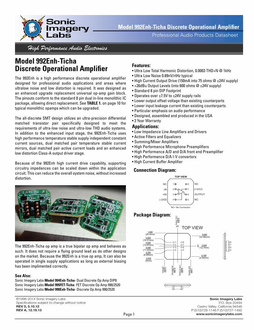
The 992Enh comes standard with a 8-pin dual in line “Pin Saver” style SMT socket and 8 gold plated “Pin Saver” pins. 4 extra pins are provided in the event that the user damages or breaks pins during installation. Utilizing the “Pin Saver” system also allows other mounting options. (See diagram below) In every mounting situation, the 992Enh operational amplifier interface is protected from accidental damage. For the vertical installation option, many connector manufacturers can provide both vertical or horizontal right angle dip socket connectors. If additional height is required, the user can add an additional standard dual in line socket to the stack to facilitate connection to the PCB. Additionally, if the user is required to mount the 992Enh to the left or right side of the existing PCB socket, a horizontal right angle display dip socket can be used and the 992Enh is simply rotated 90 degrees as shown in the side view diagram below.
©1998-2014 Sonic Imagery LabsSpecifications subject to change without noticeREV 0, 5.10.12REV A, 12.19.13
Sonic Imagery LabsP.O. Box 20494
Castro Valley, California 94546 P:(510)728-1146 F:(510)727-1492
www.sonicimagerylabs.com
1.000(25.4mm)
LC
TOP VIEW
0.000(0mm)
1.000(25.4m
m)
0.000(0m
m)
L C
0.500(12.7mm)
0.500(12.7m
m)
1234
8765
8765
PCB Reference Plane
“Pin Saver” PinsStandard Dual In-Line Socket “Pin Saver” Socket
SIDE VIEWvertical installation option
END VIEWhorizontal installation
0.365(9.27mm) 0.200
(5.08mm)
0.000(0mm) PCB Reference Plane
0.000(0mm)
Aries ElectronicsTE Electronics
Mill MaxVertical Display Socketfor vertical installation
(not supplied)
“Pin
Sav
er” P
ins
Standard Dual In-Line Socketadditional socket can be added to adjust height
Mounting, Installation Options:
Model 992Enh-Ticha Discrete Operational Amplifier
In all mounting situations, the user must keep the connection from pin � of the 992Enh to pin � of the device being replaced. Pin � of the 992Enh is identified on the bottom side of the PCB assembly. Incorrect installation will damage the 992Enh and void the warranty.
Pins 2 and 3 are the amplifiers input and thus the circuits summing junction. Flying leads, jumper wires or wire extenders are NOT recommended as this installation method degrades the amplifiers differential input circuits ability to reject common mode noise (degrades the CMRR specification), “pickup noise” and magnetically induced or radiated interference from transformers, power supplies or other noise sources.
It should also be noted that the 992Enh-Ticha op amp is a true bipolar op amp and does not require a flying ground lead as do other designs on the market. Because the 992Enh is a true op amp, It can also be operated in single supply applications as long as external biasing or bootstrapping has been designed correctly.
Page 4
©1998-2014 Sonic Imagery LabsSpecifications subject to change without noticeREV 0, 5.10.12REV A, 12.19.13
Sonic Imagery LabsP.O. Box 20494
Castro Valley, California 94546 P:(510)728-1146 F:(510)727-1492
www.sonicimagerylabs.com
Mounting, Installation Options:
Model 992Enh-Ticha Discrete Operational Amplifier
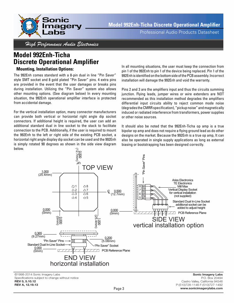
The 992Enh discrete opamps printed circuit board integrates copper clad to the collectors of the Class A output driver transistors to dissipate heat. This cladding and the associated four holes are electrically connected to VCC and VEE. These holes should not be used to mount the 992Enh opamp unless steps are taken to insulate these surfaces from the mounting surfaces by using insulating pads and non conductive hardware.
Under normal (normal being up to 60˚C / �40˚F) ambient temperature conditions, the amplifier does not require heatsinks. In applications where the 992Enh discrete op amp is used to drive very low impedances, and is operating in high ambient temperature environments, Sonic Imagery Labs can provide optional heatsinks and mounting screws designed for this package specifically.
1234
8765
Integrated HeatsinkPads, Optional Heatsink
Mounting HolesTHESE PADS ARECONNECTED TO VCC AND VEE
0.25(6.35mm)
0.00(0mm)
OPTIONAL HEATSINKPN 5250115 (2X)
OPTIONAL HEATSINKPN 5250115 (2X)
Image 1. Bottom view of 992 illustrating the location of PIN1. Note silkscreen indicator. Gold pins are “PIN SAVER” pins. Included machine socket removed for clarity.
Image 2. Optional mounting method shown with a right angle display socket. Contact Sonic Imagery Labs for additional details.
Page 5
Model 992Enh-Ticha Discrete Operational AmplifierProfessional Audio Products Datasheet
©1998-2014 Sonic Imagery LabsSpecifications subject to change without noticeREV 0, 5.10.12REV A, 12.19.13
Sonic Imagery LabsP.O. Box 20494
Castro Valley, California 94546 P:(510)728-1146 F:(510)727-1492
www.sonicimagerylabs.com
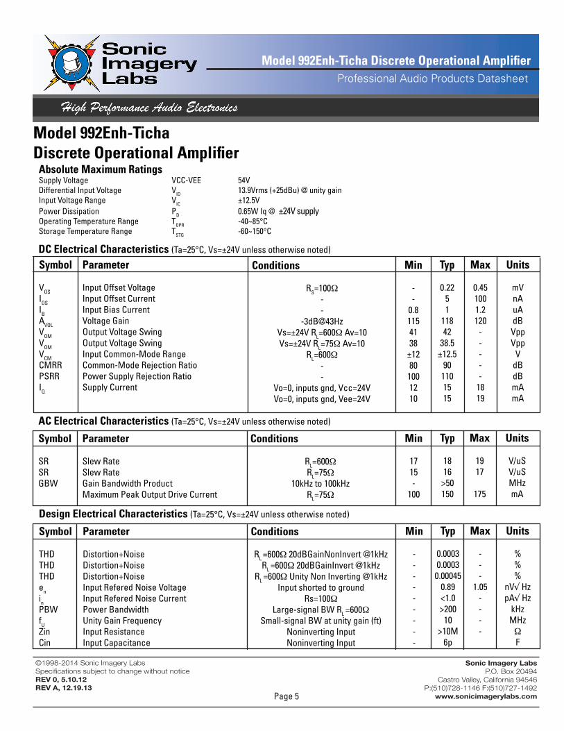
Absolute Maximum RatingsSupply Voltage VCC-VEE 54VDifferential Input Voltage VID �3.9Vrms (+25dBu) @ unity gainInput Voltage Range VIC ±�2.5VPower Dissipation PD 0.65W Iq @ ±24V supplyOperating Temperature Range TOPR -40~85°CStorage Temperature Range TSTG -60~�50°C
Model 992Enh-Ticha Discrete Operational Amplifier
Parameter
Input Offset VoltageInput Offset CurrentInput Bias CurrentVoltage GainOutput Voltage SwingOutput Voltage SwingInput Common-Mode RangeCommon-Mode Rejection RatioPower Supply Rejection RatioSupply Current
Symbol
VOSIOSIBAVOLVOMVOMVCMCMRRPSRRIQ
Conditions
RS=�00Ω--
-3dB@43HzVs=±24V RL=600Ω Av=�0Vs=±24V RL=75Ω Av=�0
RL=600Ω--
Vo=0, inputs gnd, Vcc=24VVo=0, inputs gnd, Vee=24V
Min
--
0.8��54�38
±�280
�00�2�0
Typ
0.225�
��842
38.5±�2.5
90��0�5�5
Max
0.45�00�.2�20
-----
�8�9
Units
mVnAuAdB
VppVpp
VdBdBmAmA
DC Electrical Characteristics (Ta=25°C, Vs=±24V unless otherwise noted)
Symbol
SRSRGBW
Parameter
Slew RateSlew RateGain Bandwidth ProductMaximum Peak Output Drive Current
AC Electrical Characteristics (Ta=25°C, Vs=±24V unless otherwise noted)
Conditions
RL=600ΩRL=75Ω
�0kHz to �00kHzRL=75Ω
Min
�7�5-
�00
Typ
�8�6
>50�50
Max
�9�7
�75
Units
V/uSV/uSMHzmA
Design Electrical Characteristics (Ta=25°C, Vs=±24V unless otherwise noted)
Symbol
THDTHD THDeninPBWfUZinCin
Parameter
Distortion+NoiseDistortion+NoiseDistortion+NoiseInput Refered Noise VoltageInput Refered Noise CurrentPower BandwidthUnity Gain FrequencyInput ResistanceInput Capacitance
Conditions
RL =600Ω 20dBGainNonInvert @�kHzRL =600Ω 20dBGainInvert @�kHz
RL =600Ω Unity Non Inverting @�kHzInput shorted to ground
Rs=�00ΩLarge-signal BW RL =600Ω
Small-signal BW at unity gain (ft)Noninverting InputNoninverting Input
Min
---------
Typ
0.00030.00030.00045
0.89<�.0>200
�0>�0M
6p
Max
---
�.05----
Units
%%%
nV√ HzpA√ Hz
kHzMHzΩF
Page 6
Model 992Enh-Ticha Discrete Operational AmplifierProfessional Audio Products Datasheet
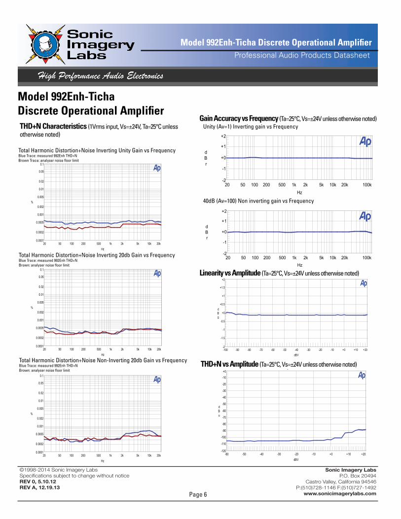
Model 992Enh-Ticha Discrete Operational AmplifierTHD+N Characteristics (�Vrms input, Vs=±24V, Ta=25°C unless otherwise noted)
©1998-2014 Sonic Imagery LabsSpecifications subject to change without noticeREV 0, 5.10.12REV A, 12.19.13
Sonic Imagery LabsP.O. Box 20494
Castro Valley, California 94546 P:(510)728-1146 F:(510)727-1492
www.sonicimagerylabs.com
Total Harmonic Distortion+Noise Inverting Unity Gain vs FrequencyBlue Trace: measured 992Enh THD+NBrown Trace: analyser noise floor limit
Total Harmonic Distortion+Noise Inverting 20db Gain vs FrequencyBlue Trace: measured 992Enh THD+NBrown: analyser noise floor limit
Total Harmonic Distortion+Noise Non-Inverting 20db Gain vs FrequencyBlue Trace: measured 992Enh THD+NBrown: analyser noise floor limit
Gain Accuracy vs Frequency (Ta=25°C, Vs=±24V unless otherwise noted)Unity (Av=�) Inverting gain vs Frequency
-2
+2
-1
+0
+1dBr
20 100k50 100 200 500 1k 2k 5k 10k 20kHz
-2
+2
-1
+0
+1dBr
20 100k50 100 200 500 1k 2k 5k 10k 20kHz
40dB (Av=�00) Non inverting gain vs Frequency
Linearity vs Amplitude (Ta=25°C, Vs=±24V unless otherwise noted)INPUT/OUTPUT LINEARITY
-2
+2
-1.5
-1
-0.5
+0
+0.5
+1
+1.5
dBg
-100 +20-90 -80 -70 -60 -50 -40 -30 -20 -10 +0 +10dBV
THD+N vs Amplitude (Ta=25°C, Vs=±24V unless otherwise noted)THD+N Ampl vs AMPLITUDE
-120
+0
-110
-100
-90
-80
-70
-60
-50
-40
-30
-20
-10
dBu
-60 +20-50 -40 -30 -20 -10 +0 +10dBV
THD+N Ratio vs FREQUENCY
0.0001
0.1
0.0002
0.0005
0.001
0.002
0.005
0.01
0.02
0.05
%
20 20k50 100 200 500 1k 2k 5k 10kHz
THD+N Ratio vs FREQUENCY
0.0001
0.1
0.0002
0.0005
0.001
0.002
0.005
0.01
0.02
0.05
%
20 20k50 100 200 500 1k 2k 5k 10kHz
THD+N Ratio vs FREQUENCY
0.0001
0.1
0.0002
0.0005
0.001
0.002
0.005
0.01
0.02
0.05
%
20 20k50 100 200 500 1k 2k 5k 10kHz

Page 7
Model 992Enh-Ticha Discrete Operational AmplifierProfessional Audio Products Datasheet
Model 992Enh-Ticha Discrete Operational Amplifier
©1998-2014 Sonic Imagery LabsSpecifications subject to change without noticeREV 0, 5.10.12REV A, 12.19.13
Sonic Imagery LabsP.O. Box 20494
Castro Valley, California 94546 P:(510)728-1146 F:(510)727-1492
www.sonicimagerylabs.com
-130
+10
-120
-110
-100
-90
-80
-70
-60
-50
-40
-30
-20
-10
+0
dB
20 200k50 100 200 500 1k 2k 5k 10k 20k 50k 100kHz
-130
+10
-120
-110
-100
-90
-80
-70
-60
-50
-40
-30
-20
-10
+0
dB
20 200k50 100 200 500 1k 2k 5k 10k 20k 50k 100kHz
Power Supply Rejection Ratio Characteristics (Ta=25°C, Vs=±24V, Rs=0 Ω, Rload=�0K Ω unless otherwise noted)
Non inverting, Unity gain (Av=�) vs Frequency, Positive Supply
Non inverting, Unity gain (Av=�) vs Frequency, Negative Supply
Open Loop Gain Frequency Response (Ta=25°C, Vs=±24V, Rload=�00K Ω unless otherwise noted)
Full Power Frequency Response (Ta=25°C, Vs=±24V, Rload=600 Ω unless otherwise noted)
-0
+30
+2
+4
+6
+8
+10
+12
+14
+16
+18
+20
+22
+24
+26
+28
dBV
10 500k20 50 100 200 500 1k 2k 5k 10k 20k 50k 100k 200kHz
+0
+130
+10
+20
+30
+40
+50
+60
+70
+80
+90
+100
+110
+120
Gain
(dB)
1 50M2 5 10 20 50 100 200 500 1k 2k 5k 10k 20k 50k 100k 500k 1M 2M 5M 10M 20MHz
Page 8
Model 992Enh-Ticha Discrete Operational AmplifierProfessional Audio Products Datasheet
Model 992Enh-Ticha Discrete Operational Amplifier
©1998-2014 Sonic Imagery LabsSpecifications subject to change without noticeREV 0, 5.10.12REV A, 12.19.13
Sonic Imagery LabsP.O. Box 20494
Castro Valley, California 94546 P:(510)728-1146 F:(510)727-1492
www.sonicimagerylabs.com
-160
+0
-140
-120
-100
-80
-60
-40
-20
dB
1 20k2 5 10 20 50 100 200 500 1k 2k 5k 10kHz
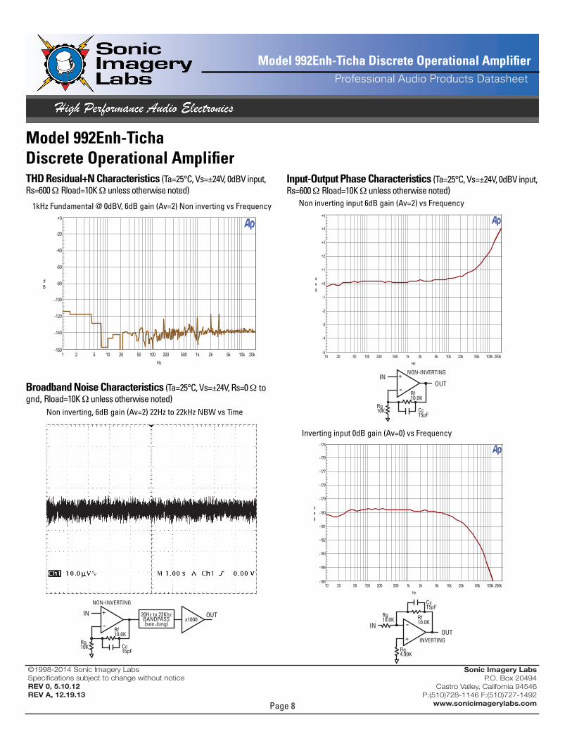
THD Residual+N Characteristics (Ta=25°C, Vs=±24V, 0dBV input, Rs=600 Ω Rload=�0K Ω unless otherwise noted)
�kHz Fundamental @ 0dBV, 6dB gain (Av=2) Non inverting vs Frequency
-5
+5
-4
-3
-2
-1
+0
+1
+2
+3
+4
deg
10 200k20 50 100 200 500 1k 2k 5k 10k 20k 50k 100kHz
-185
-175
-184
-183
-182
-181
-180
-179
-178
-177
-176
deg
10 200k20 50 100 200 500 1k 2k 5k 10k 20k 50k 100kHz
Non inverting input 6dB gain (Av=2) vs Frequency
Input-Output Phase Characteristics (Ta=25°C, Vs=±24V, 0dBV input, Rs=600 Ω Rload=�0K Ω unless otherwise noted)
Inverting input 0dB gain (Av=0) vs Frequency
+
-OUT
IN
Rf10.0K
Cc15pF
Rg10K
NON-INVERTING
+
-OUT
IN
Rg10.0K Rf
10.0K
Cc15pF
INVERTING
Rg4.99K
Broadband Noise Characteristics (Ta=25°C, Vs=±24V, Rs=0 Ω to gnd, Rload=�0K Ω unless otherwise noted)
Non inverting, 6dB gain (Av=2) 22Hz to 22kHz NBW vs Time
+
-OUTIN
Rf10.0K
Cc15pF
Rg10K
NON-INVERTING
x100020Hz to 22KhzBANDPASS(see Jung)
Page 9
Model 992Enh-Ticha Discrete Operational AmplifierProfessional Audio Products Datasheet
Model 992Enh-Ticha Discrete Operational Amplifier
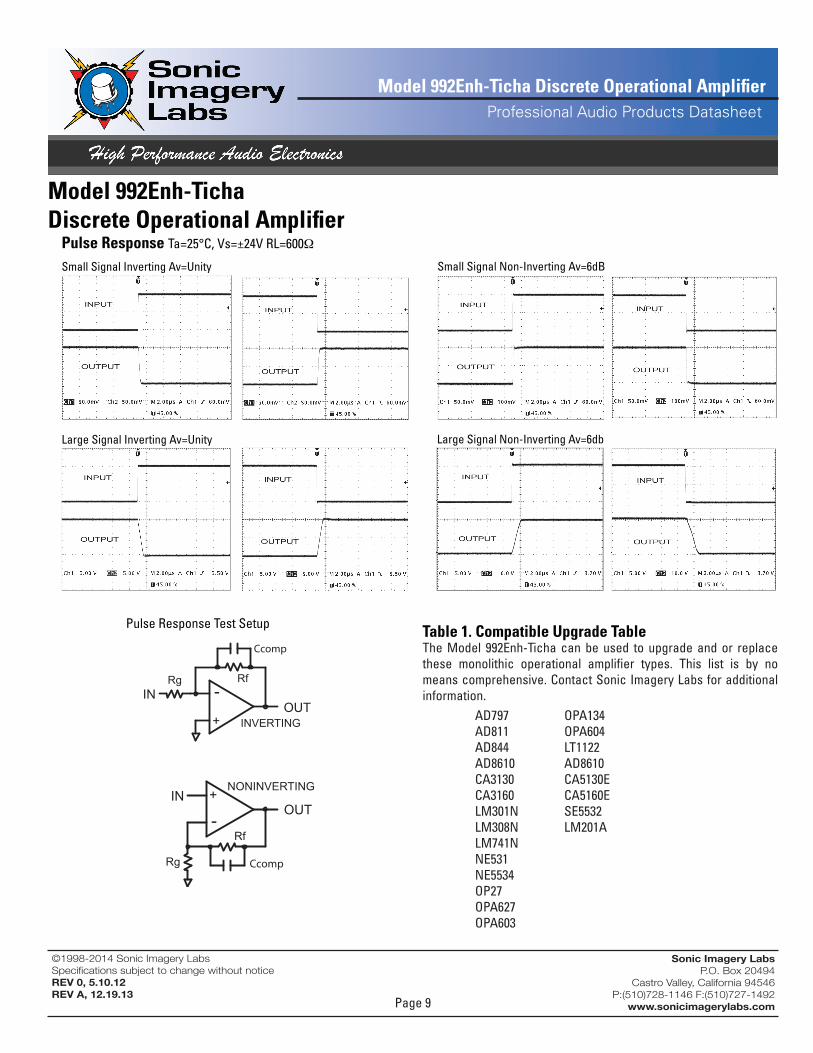
Pulse Response Ta=25°C, Vs=±24V RL=600Ω
Small Signal Inverting Av=Unity
Large Signal Inverting Av=Unity
©1998-2014 Sonic Imagery LabsSpecifications subject to change without noticeREV 0, 5.10.12REV A, 12.19.13
Sonic Imagery LabsP.O. Box 20494
Castro Valley, California 94546 P:(510)728-1146 F:(510)727-1492
www.sonicimagerylabs.com
Small Signal Non-Inverting Av=6dB
Large Signal Non-Inverting Av=6db
+
-OUT
IN
L13.6-4.3uH
Rf
CcompRg
NONINVERTING
+
-OUT
IN
L13.6-4.3uH
Rg Rf
Ccomp
INVERTING
Pulse Response Test Setup Table 1. Compatible Upgrade TableThe Model 992Enh-Ticha can be used to upgrade and or replace these monolithic operational amplifier types. This list is by no means comprehensive. Contact Sonic Imagery Labs for additional information.
AD797AD8��AD844AD86�0CA3�30CA3�60LM30�NLM308NLM74�NNE53�NE5534OP27OPA627OPA603
OPA�34OPA604LT��22AD86�0CA5�30ECA5�60ESE5532LM20�A
Page �0
Model 992Enh-Ticha Discrete Operational AmplifierProfessional Audio Products Datasheet
Model 992Enh-Ticha Discrete Operational Amplifier
Application Notes
©1998-2014 Sonic Imagery LabsSpecifications subject to change without noticeREV 0, 5.10.12REV A, 12.19.13
Sonic Imagery LabsP.O. Box 20494
Castro Valley, California 94546 P:(510)728-1146 F:(510)727-1492
www.sonicimagerylabs.com
The 992Enh is normally stable with resistive, inductive or smaller capacitive loads. Larger capacitive loads interact with the open-loop output resistance to reduce the phase margin of the feedback loop, ultimately causing oscillation.
At any loop gain setting, a feedback capacitor across the feedback resistor will aid stability. In all cases, the op amp will behave predictably only if the supplies are properly bypassed, ground loops are controlled and high-frequency feedback is derived directly from the output terminal of the 992Enh opamp.
So-called capacitive loads are not always capacitive. A high-Q capacitor in combination with long leads or PCB traces can present a series-resonant load to the op amp. In practice, this is not usually a problem; but the situation should be kept in mind.
Large capacitive loads (including series-resonant) can be accommodated by isolating the feedback path from the load as shown in Figure 1. The resistor kills the Q of series resonant circuits formed by capacitive loads. A low inductance resistor is recommended. An inductor can also be added in parallel to Riso.
+
-OUT
IN Riso24-100Ω
L13.6-4.3uH
Figure 1. Isolating capacitive loads with an resistor. The non-inductive resistor avoids resonance problems with load capacitance by isolating feedback path.
Typical Applications
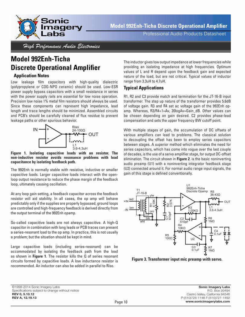
R�, R2 and C3 provide match and termination for the JT-�6-B input transformer. The step up nature of the transformer provides 5.6dB of voltage gain. R3 and R4 set ac voltage gain of the 992Enh op-amp. Whereas, R3/R4+�=Av, 20logAv=Gain_dB. Other values can be chosen depending on gain desired. C2 provides phase-lead compensation and sets the upper frequency BW cutoff point.
With multiple stages of gain, the accumulation of DC offsets of various amplifiers can lead to problems. The classical solution to decoupling the offset has been to employ series capacitors between stages. A superior method which eliminates the need for series capacitors, which has come into vogue over the last couple of decades, is the use of a servo amplifier stage, for output DC-offset elimination. The circuit shown in Figure 2. is the basic noninverting audio preamp (U�) with a noninverting integrator feedback stage (U2) connected around it. For normal audio range input signals, the gain of this stage is defined conventionally.
Low leakage film capacitors with high-quality dielectric (polypropylene or COG-NPO ceramic) should be used. Low-ESR power supply bypass capacitors with a small resistance in series with the power supply rails are essential for low noise operation. Precision low noise �% metal film resistors should always be used. Since these components can represent high impedance, lead length and trace lengths should be minimized. Assembled circuits and PCB’s should be carefully cleaned of flux residue to prevent leakage paths or other spurious behavior.
The inductor gives low output impedance at lower frequencies while providing an isolating impedance at high frequencies. Optimum values of L and R depend upon the feedback gain and expected nature of the load, but are not critical. Typical values of inductor range from 3.3uH to 4.7uH.
+
-OUT
L13.6-4.3uH
R536-43Ω
R31.00KΩ
C2510pF
+IN
-IN
red
brn
ylw
wht
orn
blk
R1
6.19
K
R2
3.57
KC
161
0pF
U1992Enh-TichaDiscrete OpampT1
JT-16-B
+
-U2
R410KΩ
R5100Ω
R61MΩ
C30.1uF
C40.1uF
R71MΩ
Figure 3. Transformer input mic preamp with servo.
Page ��
Model 992Enh-Ticha Discrete Operational AmplifierProfessional Audio Products Datasheet
©1998-2014 Sonic Imagery LabsSpecifications subject to change without noticeREV 0, 5.10.12REV A, 12.19.13
Sonic Imagery LabsP.O. Box 20494
Castro Valley, California 94546 P:(510)728-1146 F:(510)727-1492
www.sonicimagerylabs.com
Model 992Enh-Ticha Discrete Operational Amplifier
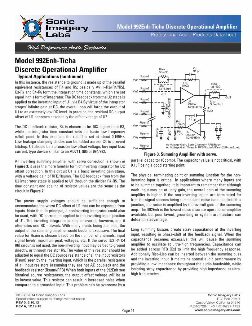
Typical Applications (continued)In this instance, the resistance to ground is made up of the parallel equivalent resistances of R4 and R5; basically Av=�+R3/(R4//R5). C3-R7 and C4-R6 form the integration time constants, which are set equal in this form of integrator. The DC feedback from the U2 stage is applied to the inverting input of U�, via R4.By virtue of the integrator stages’ infinite gain at DC, the overall loop will force the output of U� to an extremely low DC level. In practice, the residual DC output offset of U� becomes essentially the offset voltage of U2.
The DC feedback resistor, R4 is chosen to be �0X higher than R3, while the integrator time constant sets the basic low frequency rolloff point. In this example, the rolloff is set at about 0.�65Hz. Low leakage clamping diodes can be added across C4 to prevent latchup. U2 should be a precision low offset voltage, low input bias current, type device similar to an AD7��, 995 or 994/992.
An inverting summing amplifier with servo correction is shown in Figure 3; it uses the more familiar form of inverting integrator for DC offset correction. In this circuit U� is a basic inverting gain stage, with a voltage gain of RFB/Rsumn. The DC feedback from from the U2 integrator stage is applied to U� through the divider R4-R5. The time constant and scaling of resistor values are the same as the circuit in Figure 2.
The power supply voltages should be sufficient enough to accommodate the worst DC offset of U� that can be expected from inputs. Note that, in principal, a noninverting integrator could also be used, with DC correction applied to the inverting input junction of U�. The inverting integrator is simpler overall, however, and it eliminates one RC network. With many inputs being summed, the output of the summing amplifier could become excessive. The final value for Rsum is chosen based on the number of channels, input signal levels, maximum peak voltages, etc. If the servo (U2 R4 C4 R6) circuit is not used, the non-inverting input may be tied to ground directly, or through resistor R5. The value of this resistor should be adjusted to equal the DC source resistance of all the input resistors (Rsum) seen by the inverting input, which is the parallel resistance of all input resistors (assuming they are not AC coupled) and the feedback resistor (Rsum//RFB) When both inputs of the 992Enh see identical source resistances, the output offset voltage will be at its lowest value. This resistor can result in increased noise when compared to a grounded input. This problem can be overcome by a
+
-OUT
Liso3.6-4.3uH
Riso36-43Ω
RFB10KΩ
Cx91 pF
U1992Enh1/2 994Enh
+
-U2992Enh1/2 994Enh
R4100KΩ
R51KΩ
R61MΩ
C40.1uF
Liso3.6-4.3uH
Riso36-43Ω
JP1
Vin1
Vin2
Vin3
Vin4
Vinx
Viny
Vinz
Rsum1
Rsum2
Rsum3
Rsum4
Rsumx
Rsumy
Rsumz
STR
AYC
APA
CIT
AN
CE
Ac Voltage Gain, Each Channel= RFB/RsumAc Voltage Gain Overall= RFB/Rsum1//Rsum2//Rsum3...etc
JP2
Cco
mp
Figure 3. Summing Amplifier with servo.parallel capacitor (Ccomp). The capacitor value is not critical, with 0.�uF being a good starting point.
The physical terminating point or summing junction for the non-inverting input is critical. In applications where many inputs are to be summed together, it is important to remember that although each input may be at unity gain, the overall gain of the summing amplifier is higher. If the non-inverting inputs are terminated far from the signal sources being summed and noise is coupled into this junction, the noise is amplified by the overall gain of the summing amp. The 992Enh is the lowest noise discrete operational amplifier available, but poor layout, grounding or system architecture can defeat this advantage.
Long summing busses create stray capacitance at the inverting input, resulting in phase-shift of the feedback signal. When the capacitance becomes excessive, this will cause the summing amplifier to oscillate at ultra-high frequencies. Capacitance can be added across RFB (Cx) to limit the high frequency response. Additionally Riso-Liso can be inserted between the summing buss and the inverting input. It maintains normal audio performance by providing a low impedance throughout the audio bandwidth, while isolating stray capacitance by providing high impedance at ultra-high frequencies.
Page �2
Model 992Enh-Ticha Discrete Operational AmplifierProfessional Audio Products Datasheet
©1998-2014 Sonic Imagery LabsSpecifications subject to change without noticeREV 0, 5.10.12REV A, 12.19.13
Sonic Imagery LabsP.O. Box 20494
Castro Valley, California 94546 P:(510)728-1146 F:(510)727-1492
www.sonicimagerylabs.com
Model 992Enh-Ticha Discrete Operational Amplifier
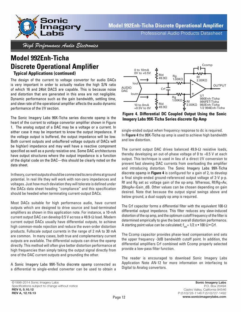
Typical Applications (continued)The design of the current to voltage convertor for audio DACs is very important in order to actually realize the high S/N ratio of which �6 and 24bit DACS are capable. This is because noise and distortion that are generated in this area are not negligible. Dynamic performance such as the gain bandwidth, settling time, and slew rate of the operational amplifier affects the audio dynamic performance of the I/V section.
The Sonic Imagery Labs 99X-Ticha series discrete opamp is the heart of the current to voltage convertor amplifier shown in Figure �. The analog output of a DAC may be a voltage or a current. In either case it may be important to know the output impedance. If the voltage output is buffered, the output impedance will be low. Both current outputs and unbuffered voltage outputs of DACs will be high(er) impedance and may well have a reactive component specified as well as a purely resistive one. Some DAC architectures have output structures where the output impedance is a function of the digital code on the DAC—this should be clearly noted on the data sheet.
In theory, current outputs should be connected to zero ohms at ground potential. In real life they will work with non-zero impedances and voltages. Just how much deviation they will tolerate is defined under the DACs data sheet heading “compliance” and this specification should be heeded when terminating current-output DACs.
Most DACs suitable for high performance audio, have current outputs which are designed to drive source and load-terminated amplifiers as shown in this application note. For instance, a �0-mA current output DAC can develop 0.5 V across a 49.9-Ω load. Modern current output DACs usually have differential outputs, to achieve high common-mode rejection and reduce the even-order distortion products. Fullscale output currents in the range of 2 mA to 30 mA are common. In many cases, both true and complementary current outputs are available. The differential outputs can drive the opamp directly. This method will often give better distortion performance at high frequencies than simply taking the output signal directly from one of the DAC current outputs and grounding the other.
A Sonic Imagery Labs 99X-Ticha discrete opamp connected as a differential to single-ended converter can be used to obtain a
single-ended output when frequency response to dc is required. In Figure 4 the 99X-Ticha op amp is used to achieve high bandwidth and low distortion.
The current output DAC drives balanced 49.9-Ω resistive loads, thereby developing an out-of-phase voltage of 0 to +0.5 V at each output. This technique is used in lieu of a direct I/V conversion to prevent fast slewing DAC currents from overloading the amplifier and introducing distortion. The Sonic Imagery Labs 99X-Ticha discrete opamp in Figure 4 is configured for a gain of 2, to develop a final single-ended ground-referenced output voltage of 2-V p-p. Rf and Rg set ac voltage gain of the op-amp. Whereas, Rf/Rg=Av, 20logAv=Gain_dB. Other values can be chosen depending on gain desired. Note that because the output signal swings above and below ground, a dual-supply op amp is required.
The Crf capacitor forms a differential filter with the equivalent �00-Ω differential output impedance. This filter reduces any slew-induced distortion of the op amp, and the optimum cutoff frequency of the filter is determined empirically to give the best overall distortion performance. A starting point value can be calculated; f3db= �/2 π • �00 Ω • Crf.
The Ccomp capacitor provides phase-lead compensation and sets the upper frequency -3dB bandwidth cutoff point. In addition, the differential amplifiers Crf combined with Ccomp properly selected provide a low-pass filter function.
The reader is encouraged to download Sonic Imagery Labs Application Note AN-�2 for more information on interfacing to Digital to Analog convertors.
Rld49.9Ω
+
-Rf2.00KΩ
Crf
U1990Enh-Ticha995FET-Ticha992Enh-Ticha1/2 994Enh-Ticha
Rf2.00KΩ
Rld49.9Ω
Ccomp
Iout
Ioutn
AUDIODAC
0 to 10mA0V to +0.5V
10 to 0mA+0.5V to 0V
Rg1.00KΩ
Rg1.00KΩ
OUTPUT
Figure 4. Differential DC Coupled Output Using the Sonic Imagery Labs 99X-Ticha Series discrete Op Amp
Page �3
Model 992Enh-Ticha Discrete Operational AmplifierProfessional Audio Products Datasheet
©1998-2014 Sonic Imagery LabsSpecifications subject to change without noticeREV 0, 5.10.12REV A, 12.19.13
Sonic Imagery LabsP.O. Box 20494
Castro Valley, California 94546 P:(510)728-1146 F:(510)727-1492
www.sonicimagerylabs.com
Model 992Enh-Ticha Discrete Operational Amplifier
THE CONTENTS OF THIS DOCUMENT ARE PROVIDED IN CONNECTION WITH Sonic Imagery Labs PRODUCTS. Sonic Imagery Labs MAKES NO REPRESENTATIONS OR WARRANTIES WITH RESPECT TO THE ACCURACY OR COMPLETENESS OF THE CONTENTS OF THIS PUBLICATION AND RESERVES THE RIGHT TO MAKE CHANGES TO SPECIFICATIONS AND PRODUCT DESCRIPTIONS AT ANY TIME WITHOUT NOTICE. NO LICENSE, WHETHER EXPRESS, IMPLIED, ARISING BY ESTOPPEL OR OTHERWISE, TO ANY INTELLECTUAL PROPERTY RIGHTS IS GRANTED BY THIS DOCUMENT.
TESTING AND OTHER QUALITY CONTROLS ARE USED TO THE EXTENT Sonic Imagery Labs DEEMS NECESSARY TO SUPPORT Sonic Imagery Labs PRODUCT WARRANTY. TESTING OF ALL PUBLISHED PARAMETERS AND SPECIFICATIONS OF EACH PRODUCT IS PERFORMED BEFORE SHIPMENT. Sonic Imagery Labs ASSUMES NO LIABILITY FOR APPLICATIONS ASSISTANCE OR BUYER PRODUCT DESIGN. BUYERS ARE RESPONSIBLE FOR THEIR PRODUCTS AND APPLICATIONS USING Sonic Imagery Labs PRODUCTS. PRIOR TO USING OR DISTRIBUTING ANY PRODUCTS THAT INCLUDE Sonic Imagery Labs COMPONENTS, BUYERS SHOULD PROVIDE ADEQUATE DESIGN, TESTING AND OPERATING SAFEGUARDS.
EXCEPT AS PROVIDED IN Sonic Imagery Labs TERMS AND CONDITIONS OF SALE FOR SUCH PRODUCTS, Sonic Imagery Labs ASSUMES NO LIABILITY WHATSOEVER, AND Sonic Imagery Labs DISCLAIMS ANY EXPRESS OR IMPLIED WARRANTY RELATING TO THE SALE AND/OR USE OF Sonic Imagery Labs PRODUCTS INCLUDING LIABILITY OR WARRANTIES RELATING TO FITNESS FOR A PARTICULAR PURPOSE, MERCHANTABILITY, OR INFRINGEMENT OF ANY PATENT, COPYRIGHT OR OTHER INTELLECTUAL PROPERTY RIGHT.
LIFE SUPPORT AND CRITICAL COMPONENTS POLICYSonic Imagery Labs PRODUCTS ARE NOT AUTHORIZED FOR USE AS CRITICAL COMPONENTS IN LIFE SUPPORT DEVICES OR CRITICAL SYSTEMS WITHOUT THE EXPRESS PRIOR WRITTEN APPROVAL OF THE CHIEF EXECUTIVE OFFICER AND GENERAL COUNSEL OF Sonic Imagery Labs. As used herein:
Life support devices or systems are devices which (a) are intended for surgical implant into the body, or (b) support or sustain life and whose failure to perform when properly used in accordance with instructions for use provided in the labeling can be reasonably expected to result in a significant injury to the user. A critical component is any component in a life support device or system whose failure to perform can be reasonably expected to cause the failure of the life support device or system or to affect its safety or effectiveness.
Typical Applications (continued)
The previous applications focused on technical situations a designer might find themselves faced with that requires some technical cognizance while designing new projects.
A trend that has come into vogue during the DIY resurgence of the last few years is the rebuilding, refurbishing or “reamping” of audio gear. The 99X series of op-amps is perfectly suited for this trend and in most cases can simply be dropped into existing sockets. Because the 99X series of opamps electrical specifications are typically superior to older monolithic devices, can operate over a wider range of supply rails, and is a true opamp, the user is typically not required to modify the existing support circuitry.
In most cases, if the existing circuitry surrounding the operational amplifier was originally designed correctly, and with particular emphasis on low noise and low distortion audio performance, “reamping” with a 99X series discrete opamp will improve those specifications.
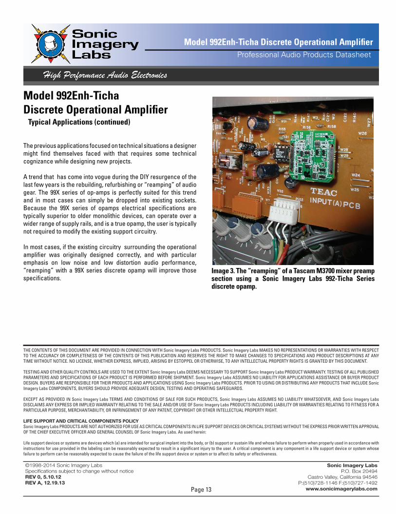
Image 3. The “reamping” of a Tascam M3700 mixer preamp section using a Sonic Imagery Labs 992-Ticha Series discrete opamp.