Mercury Programmable Logic Device Family Data Sheet
86
® Altera Corporation 1 Mercury Programmable Logic Device Family January 2003, ver. 2.2 Data Sheet DS-MERCURY-2.2 13 Tools Features… ■ High-performance programmable logic device (PLD) family (see Table 1) – Integrated high-speed transceivers with support for clock data recovery (CDR) at up to 1.25 gigabits per second (Gbps) – Look-up table (LUT)-based architecture optimized for high speed – Advanced interconnect structure for fast routing of critical paths – Enhanced I/O structure for versatile standards and interface support – Up to 14,400 logic elements (LEs) ■ System-level features – Up to four general-purpose phase-locked loops (PLLs) with programmable multiplication and delay shifting – Up to 12 PLL output ports – Dedicated multiplier circuitry for high-speed implementation of signed or unsigned multiplication up to 16 × 16 – Embedded system blocks (ESBs) used to implement memory functions including quad-port RAM, true dual-port RAM, first- in first-out (FIFO) buffers, and content-addressable memory (CAM) – Each ESB contains 4,096 bits and can be split and used as two 2,048-bit unidirectional dual-port RAM blocks Note to Table 1: (1) Each ESB can be used for two dual- or single-port RAM blocks. Table 1. Mercury Device Features Feature EP1M120 EP1M350 Typical gates 120,000 350,000 HSDI channels 8 18 LEs 4,800 14,400 ESBs (1) 12 28 Maximum RAM bits 49,152 114,688 Maximum user I/O pins 303 486
Transcript of Mercury Programmable Logic Device Family Data Sheet

®
MercuryProgrammable Logic
Device Family
January 2003, ver. 2.2 Data Sheet
Developm
ent
13
Tools
Features… High-performance programmable logic device (PLD) family (see Table 1)– Integrated high-speed transceivers with support for clock data
recovery (CDR) at up to 1.25 gigabits per second (Gbps)– Look-up table (LUT)-based architecture optimized for high
speed– Advanced interconnect structure for fast routing of critical paths– Enhanced I/O structure for versatile standards and interface
support– Up to 14,400 logic elements (LEs)
System-level features– Up to four general-purpose phase-locked loops (PLLs) with
programmable multiplication and delay shifting – Up to 12 PLL output ports– Dedicated multiplier circuitry for high-speed implementation of
signed or unsigned multiplication up to 16 × 16– Embedded system blocks (ESBs) used to implement memory
functions including quad-port RAM, true dual-port RAM, first-in first-out (FIFO) buffers, and content-addressable memory (CAM)
– Each ESB contains 4,096 bits and can be split and used as two 2,048-bit unidirectional dual-port RAM blocks
Note to Table 1:(1) Each ESB can be used for two dual- or single-port RAM blocks.
Table 1. Mercury Device Features
Feature EP1M120 EP1M350
Typical gates 120,000 350,000
HSDI channels 8 18
LEs 4,800 14,400
ESBs (1) 12 28
Maximum RAM bits 49,152 114,688
Maximum user I/O pins 303 486
Altera Corporation 1
DS-MERCURY-2.2

Mercury Programmable Logic Device Family Data Sheet
...and More Features
Advanced high-speed I/O features– Robust I/O standard support, including LVTTL, PCI up to
66 MHz, 3.3-V AGP in 1× and 2× modes, 3.3-V SSTL-3 and 2.5-V SSTL-2, GTL+, HSTL, CTT, LVDS, LVPECL, and 3.3-V PCML
– High-speed differential interface (HSDI) with dedicated circuitry for CDR at up to 1.25 Gbps for LVDS, LVPECL, and 3.3-V PCML
– Support for source-synchronous True-LVDSTM circuitry up to 840 megabits per second (Mbps) for LVDS, LVPECL, and 3.3-V PCML
– Up to 18 input and 18 output dedicated differential channels of high-speed LVDS, LVPECL, or 3.3-V PCML
– Built-in 100-Ω termination resistor on HSDI data and clock differential pairs
– Flexible-LVDSTM circuitry provides 624-Mbps support on up to 100 channels with the EP1M350 device
– Versatile three-register I/O element (IOE) supporting double data rate I/O (DDRIO), double data-rate (DDR) SDRAM, zero bus turnaround (ZBT) SRAM, and quad data rate (QDR) SRAM
Designed for low-power operation – 1.8-V internal supply voltage (VCCINT)– MultiVoltTM I/O interface voltage levels (VCCIO) compatible
with 1.5-V, 1.8-V, 2.5-V, and 3.3-V devices– 5.0-V tolerant with external resistor
Advanced interconnect structure– Multi-level FastTrack® Interconnect structure providing fast,
predictable interconnect delays– Optimized high-speed Priority FastTrack Interconnect for
routing critical paths in a design– Dedicated carry chain that implements arithmetic functions such
as fast adders, counters, and comparators (automatically used by software tools and megafunctions)
– FastLUTTM connection allowing high speed direct connection between LEs in the same logic array block (LAB)
– Leap lines allowing a single LAB to directly drive LEs in adjacent rows
– The RapidLAB interconnect providing a high-speed connection to a 10-LAB-wide region
– Dedicated clock and control signal resources, including four dedicated clocks, six dedicated fast global signals, and additional row-global signals
2 Altera Corporation

Mercury Programmable Logic Device Family Data Sheet
Developm
ent
13
Tools
Tables 2 and 3 show the MercuryTM FineLine BGATM device package sizes, options, and I/O pin counts.
General Description
Mercury devices integrate high-speed differential transceivers and support for CDR with a speed-optimized PLD architecture. These transceivers are implemented through the dedicated serializer, deserializer, and clock recovery circuitry in the HSDI and incorporate support for the LVDS, LVPECL, and 3.3-V PCML I/O standards. This circuitry, together with enhanced I/O elements (IOEs) and support for numerous I/O standards, allows Mercury devices to meet high-speed interface requirements.
Mercury devices are the first PLDs optimized for core performance. These LUT-based, enhanced memory devices use a network of fast routing resources to achieve optimal performance. These resources are ideal for data-path, register-intensive, mathematical, digital signal processing (DSP), or communications designs.
Table 2. Mercury Package Sizes
Feature 484-Pin FineLine BGA
780-Pin FineLine BGA
Pitch (mm) 1.00 1.00
Area (mm2) 529 841
Length × width (mm × mm) 23 × 23 29 × 29
Table 3. Mercury Package Options & I/O Count
Device 484-Pin FineLine BGA
780-Pin FineLine BGA
EP1M120 303
EP1M350 486
Altera Corporation 3

Mercury Programmable Logic Device Family Data Sheet
Mercury devices include other features for performance such as quad-port RAM, CAM, general purpose PLLs, and dedicated circuitry for implementing multiplier circuits. Table 4 shows Mercury performance.
Note to Table 4:(1) The clock tree supports up to 400 MHz. Although the registered performance for these designs exceed 400 MHz,
they are limited by the clock tree limit.
Configuration
The logic, circuitry, and interconnects in the Mercury architecture are configured with CMOS SRAM elements. Mercury devices are reconfigurable and are 100% tested prior to shipment. As a result, test vectors do not have to be generated for fault coverage purposes. Instead, the designer can focus on simulation and design verification. In addition, the designer does not need to manage inventories of different ASIC designs; Mercury devices can be configured on the board for the specific functionality required.
Mercury devices are configured at system power-up with data stored in an Altera® serial configuration device or provided by a system controller. Altera offers in-system programmability (ISP)-capable configuration devices, which configure Mercury devices via a serial data stream. Mercury devices can be configured in under 70 ms. Moreover, Mercury devices contain an optimized interface that permits microprocessors to configure Mercury devices serially or in parallel, synchronously or asynchronously. This interface also enables microprocessors to treat Mercury devices as memory and to configure the device by writing to a virtual memory location, simplifying reconfiguration.
Table 4. Mercury Performance
Application Resources Used Performance
LEs ESBs -5 Speed Grade
-6 Speed Grade
-7 Speed Grade
Units
16-bit loadable counter (1) 16 0 400 400 400 MHz
32-bit loadable counter (1) 32 0 400 400 400 MHz
32-bit accumulator (1) 32 0 400 400 400 MHz
32-to-1 multiplexer 27 0 1.864 2.466 2.723 ns
32 × 64 asynchronous FIFO 103 2 290 258 242 MHz
8-bit, 37-tap FIR filter 251 1 290 240 205 MSPS
4 Altera Corporation

Mercury Programmable Logic Device Family Data Sheet
Developm
ent
13
Tools
After a Mercury device has been configured, it can be reconfigured in-circuit by resetting the device and loading new data. Real-time changes can be made during system operation, enabling innovative reconfigurable computing applications.
Software
Mercury devices are supported by the Altera QuartusTM II development system, a single, integrated package that offers HDL and schematic design entry, compilation and logic synthesis, full simulation and worst-case timing analysis, SignalTapTM logic analysis, and device configuration. The Quartus II software also ships with Altera-specific HDL synthesis tools from Exemplar Logic and Synopsys, and Altera-specific Register Transfer Level (RTL) and timing simulation tools from Model Technology. The Quartus II software supports PCs running Windows 98, Windows NT 4.0, and Windows 2000; UNIX workstations running Solaris 2.6, 7, or 8, or HP-UX 10.2 or 11.0; and PCs running Red Hat Linux 7.1.
The Quartus II software provides NativeLinkTM interfaces to other industry-standard PC- and UNIX-workstation-based EDA tools. For example, designers can invoke the Quartus II software from within the Mentor Graphics LeonardoSpectrum software, Synplicity’s Synplify software, and the Synopsys FPGA Express software. The Quartus II software also contains built-in optimized synthesis libraries; synthesis tools can use these libraries to optimize designs for Mercury devices. For example, the Synopsys Design Compiler library, supplied with the Quartus II development system, includes DesignWare functions optimized for the Mercury architecture.
For more information on the Quartus II development system, see the Quartus II Programmable Logic Development System & Software Data Sheet.
Functional Description
The Mercury architecture contains a row-based logic array to implement general logic and a row-based embedded system array to implement memory and specialized logic functions. Signal interconnections within Mercury devices are provided by a series of row and column interconnects with varying lengths and speeds. The priority FastTrack Interconnect structure is faster than other interconnects; the Quartus II Compiler places design-critical paths on these faster lines to improve design performance.
Altera Corporation 5

Mercury Programmable Logic Device Family Data Sheet
Mercury device I/O pins are evenly distributed across the entire device area; other Altera device families have I/O pins placed on the device periphery. Mercury device I/O pin placement allows for higher I/O count at a given die size; pad size is no longer a limiting issue. Each I/O pin is fed by an IOE. IOEs are grouped in IOE row bands from the top to the bottom of the device. IOE row bands are separated by several LAB rows. LABs from the associated LAB row closest to the I/O row band drive IOEs through the local interconnect. This feature allows fast clock-to-output times when a pin is driven by any of the 10 LEs in the adjacent associated LAB. Each IOE contains a bidirectional buffer along with an input register, output register, output enable (OE) register, and input latch for DDR. When used with a global clock, these dedicated registers provide exceptional bidirectional I/O performance.
IOEs provide a variety of features, such as 3.3-V, 64-bit, 66-MHz PCI compliance; 3.3-V, 64-bit, 133-MHz PCI-X compliance; Joint Test Action Group (JTAG) boundary-scan test (BST) support; output drive strength control; slew-rate control; tri-state buffers; bus-hold circuitry; programmable pull-up resisters; programmable input and output delays; and open-drain outputs. Mercury devices offer enhanced I/O support, including support for 1.8-V I/O, 2.5-V I/O, LVCMOS, LVTTL, HSTL, LVPECL, 3.3-V PCML, 3.3-V PCI, PCI-X, LVDS, GTL+, SSTL-2, SSTL-3, CTT, and 3.3-V AGP I/O standards. CDR (up to 1.25 Gbps) and source-synchronous (up to 840 Mbps) transfers are supported with HSDI circuitry for LVDS, LVPECL, and 3.3-V PCML I/O standards.
The ESB can implement a variety of memory functions, including CAM, quad-port RAM, true dual-port RAM, dual- and single-port RAM, ROM, and FIFO functions. ESBs are grouped into two rows: one at the top and one at the bottom of the device. Embedding the memory directly into the die improves performance and reduces die area compared to distributed-RAM implementations. Moreover, the abundance of cascadable ESBs, in conjunction with the ability for one ESB to implement two separate memory blocks, ensures that the Mercury device can implement multiple wide memory blocks for high-density designs. The ESB’s high speed ensures the implemention of small memory blocks without any speed penalty. The abundance of ESBs ensures that designers can create as many different-sized memory blocks as the system requires. Figure 1 shows an overview of the Mercury device.
6 Altera Corporation

Mercury Programmable Logic Device Family Data Sheet
Developm
ent
13
Tools
Figure 1. Mercury Architecture Block Diagram Note (1)
Note to Figure 1:(1) Figure 1 shows an EP1M120 device. Mercury devices have a varying number of rows, columns, and ESBs, as shown
in Table 5.
Table 5 lists the resources available in Mercury devices.
Associated LAB Row
Buried LAB Row
Buried LAB Row
Associated LAB Row
Buried LAB Row
Buried LAB Row
Associated LAB Row
Buried LAB Row
Buried LAB Row
Associated LAB Row
Associated LAB Row
Buried LAB Row
ESB ESB ESB ESB ESB ESB
ESB ESB ESB ESB ESB ESB
Local Interconnect: Connects LEs withinthe Same or AdjacentLABs
Row and Priority Row Interconnect: ConnectsLABs within a Row
Column and PriorityColumn Interconnect: Connects LABs within Different Rows (Top to Bottom)
Leap Lines: ConnectsAdjacent LABs in Same Column
RapidLAB Interconnect:Connects Any 10Consecutive LABswithin a Row froma Central LAB
I/O Band with HSDI
I/O Band
I/O Band
I/O Band
I/O Band
Table 5. Mercury Device Resources
Device LAB Rows LAB Columns I/O Row Bands ESBs
EP1M120 12 40 5 12
EP1M350 18 80 4 28
Altera Corporation 7
Mercury Programmable Logic Device Family Data Sheet
Mercury devices provide four dedicated clock input pins and six dedicated fast I/O pins that globally drive register control inputs, including clocks. These signals ensure efficient distribution of high-speed, low-skew control signals. The control signals use dedicated routing channels to provide short delays and low skew. The dedicated fast signals can also be driven by internal logic, providing an ideal solution for a clock divider or internally generated asynchronous control signal with high fan-out. The dedicated clock and fast I/O pins on Mercury devices can also feed logic. Dedicated clocks can also be used with the Mercury general purpose PLLs for clock management.
Each I/O row band also provides two additional I/O pins that can drive two row-global signals. Row-global signals can drive register control inputs for the LAB row associated with that particular I/O row band.
High-Speed Differential Interface
The top I/O or HSDI band in Mercury devices contains dedicated circuitry for supporting differential standards at speeds up to 1.25 Gbps. Mercury devices have dedicated differential buffers and circuitry to support LVDS, LVPECL, and 3.3-V PCML I/O standards. Two dedicated high-speed PLLs (separate from the general purpose PLLs) multiply reference clocks and drive high-speed differential serializer/deserializer channels. In addition, clock recovery units (CRUs) at each receiver channel enable CDR. EP1M120 devices support eight input channels, eight output channels, and two dedicated clock inputs for feeding the receiver and/or transmitter PLLs. EP1M350 devices support 18 input channels, 18 output channels, and two dedicated clock inputs.
Mercury devices have optional built-in 100-Ω termination resistors on HSDI differential receiver data pins and the HSDI_CLK1 and HSDI_CLK2 pins.
Designers can use the HSDI circuitry for the following applications:
Gigabit Ethernet backplanes ATM, SONET RapidIO POS-PHY Level 4 Fibre Channel SDTV
The HSDI band supports one of two possible modes:
Source-synchronous mode Clock data recovery (CDR) mode
8 Altera Corporation

Mercury Programmable Logic Device Family Data Sheet
Developm
ent
13
Tools
In source-synchronous mode, source synchronous interfacing is supported at up to 840 Mbps. Serial channels are transmitted and received along with a low speed clock. The receiving device then multiplies the clock by a factor of 1 to 12, 14, 16, 18, or 20. The serialization/ deserialization rate can be any number from 4, 7, 8, 9 to 12, 14, 16, 18, or 20 and does not have to equal the clock multiplication value. For example, an 840-Mbps LVDS channel can be received along with a 84-MHz clock. The 84-MHz clock is multiplied by 10 to drive the serial shift register, but the register can be clocked out in parallel at 7-, 8-, 9- to 12-, 14-, 16-, 18-, or 20-bits wide at 42 to 120 MHz. See Figures 2 and 3.
Figure 2. Receiver Diagram for Source Synchronous Mode Notes (1), (2)
Notes to Figure 2:(1) EP1M350 devices have 18 individual receiver channels. EP1M120 devices have 8 individual receiver channels.(2) W = 1 to 12, 14, 16, 18, or 20
J = 4, 7, 8, 9 to 12, 14, 16, 18, or 20W does not have to equal J.
(3) This clock pin drives an HSDI PLL only. It does not drive to the core.
+—
ReceiverChannel
+—
ReceiverChannel
+—
ReceiverChannel
HSDI_CLK2 (3) HSDIPLL2
×W1
J
Deserializer Data toLEs
To GlobalClock
Receiver Channel 1
Receiver Channel 8
Receiver Channel 2
J Bits Wide
Altera Corporation 9

Mercury Programmable Logic Device Family Data Sheet
Figure 3. Transmitter Diagram for Source Synchronous Mode Notes (1), (2)
Notes to Figure 3:(1) EP1M350 devices have 18 individual transmitter channels. EP1M120 devices have 8 individual transmitter
channels.(2) W = 1 to 12, 14, 16, 18, or 20
B = 1 to 12, 14, 16, 18, or 20J = 4, 7, 8, 9 to 12, 14, 16, 18, or 20W, B, and J do not have to be equal.
(3) This clock pin drives an HSDI PLL only. It does not drive to the logic array.
The Mercury device’s source-synchronous mode also supports the RapidIO interface protocol at up to 500 Mbps using the LVDS I/O standard.
f For more information on source synchronous interfacing see AN 159: Using HSDI in Source-Synchronous Mode in Mercury Devices.
TransmitterChannel
HSDI_CLK1 (3)
Global Clockfrom Receiveror System Clock HSDI
PLL1
×W
×
1
J
Serializer Data fromLEs
Transmitter Channel 1
J Bits Wide
TransmitterChannel
Transmitter Channel 2
TransmitterChannel
Transmitter Channel 8
TXOUTCLOCK
WB
10 Altera Corporation

Mercury Programmable Logic Device Family Data Sheet
Developm
ent
13
Tools
Table 6 defines the support for source-synchronous mode applications.
Note to Table 6:(1) You can use the CDR circuit to achieve data rates for DC coupled LVDS
applications. You must AC-couple the clock to a 2.2-V common mode voltage (VCM) using the AC-coupling schemes in AN 134: Using Programmable I/O Standards in Mercury Devices. The data channels should be DC-coupled. The byte alignment relative to the clock is lost when using the CDR circuit. Therefore, a byte-alignment circuit is required. Most Mercury source-synchronous designs already include byte-alignment logic since they usually use DDR or SDR clocks. The CDR run length requirement is waived if the reference clock and the receiver data come from the same source and have the same frequency.
In CDR mode, serial data is supported up to 1.25 Gbps per channel. The system provides a reference clock which is multiplied by the receiver or transmitter PLL to the same rate as the data is provided. For the receiver, this multiplied reference clock is used by a CRU on each receiver channel to generate a recovered clock in-phase with the received data. That recovered clock drives the programmable deserializer and synchronizer. The synchronizer is a FIFO for data transfer between the recovered clock domain and the global clock domain. The dedicated synchronizers can be bypassed if necessary. For every receiver channel in the EP1M350 and EP1M120 devices, the ÷J recovered clock can drive a priority column line for use as a clock. See Figure 4.
Table 6. Source-Synchronous Mode
Data Rate I/O Standard
LVDS LVPECL 3.3-V PCML
≤ 840 Mbps (1) v v
Altera Corporation 11

Mercury Programmable Logic Device Family Data Sheet
Figure 4. Receiver & Transmitter Diagrams for CDR Mode Notes (1), (2)
÷J
Dat
a J
Syn
chro
nize
r
Des
eria
lizer
DP
LL
Dat
a J
RC
LK
+—
Syn
chro
nize
r
Ser
ializ
er
Dat
a J
Syn
chro
nize
r
Des
eria
lizer
DP
LL
Dat
a(3
)(3
)
J
RC
LK
+—
Syn
chro
nize
r
Ser
ializ
er
+—
+—
PLL
2 8
TX
4 (T
X9)
RX
4 (R
X9)
TX
5 (T
X10
)R
X5
(RX
10)
HS
DI_
CLK
1 (5
)H
SD
I_C
LK2
(5)
(4)
(4)
(4)
(4)
RE
FC
LK
PLL
1 8
RE
FC
LK
GC
LK4
GC
LK3
GC
LK2
GC
LK1
4 De
dica
ted
Cloc
ks
× W
× W
÷J÷J
Dat
a J
Syn
chro
nize
r
Des
eria
lizer
DP
LL
Dat
a J
RC
LK
+—
Syn
chro
nize
r
Ser
ializ
er
(3)
TX
3 (T
X8)
RX
3 (R
X8)
÷J÷J
÷J
Dat
a J
Syn
chro
nize
r
Des
eria
lizer
DP
LL
Dat
a(3
)
J
RC
LK
+—
Syn
chro
nize
r
Ser
ializ
er
TX
6 (T
X11
)R
X6
(RX
11)
÷J÷J
12 Altera Corporation

Mercury Programmable Logic Device Family Data Sheet
Developm
ent
13
Tools
Notes to Figure 4:(1) EP1M350 devices have 18 individual receiver and transmitter channels. EP1M120
devices have 8 individual receiver and transmitter channels. Receiver and transmitter channel numbers in parenthesis are for EP1M350 devices.
(2) W = 1 to 12, 14, 16, 18, or 20J = 3 to 12, 14, 16, 18, or 20W does not have to equal J.
(3) For every receiver channel in EP1M350 and EP1M120 devices, the ÷J recovered clock can drive the priority column interconnect for use as a clock.
(4) The two center channels adjacent to the HSDI PLLs (channels 4 and 5 for EP1M120 devices, channels 9 and 10 for EP1M350 devices) can drive the Mercury device’s global clocks.
(5) HSDI_CLK1 and HSDI_CLK2 pins must be differential. These clock pins drive HSDI PLLs only. They do not drive to the logic array.
The multiplied reference clock is also used to synchronize and serialize at the transmitter side.
Up to two different serial data rates are supported for input channels or output channels. Received data must be non-return-to-zero (NRZ).
Table 7 defines the support for CDR-mode applications. Table 8 shows the supported data rates for each speed grade.
Notes to Table 7:(1) The VCM operating range for AC-coupled applications is from 0 to 0.7 V and from 1.8 to 2.4 V.(2) Use AC-coupled LVDS or another I/O standard. The DC-coupled LVDS I/O standard provides performance up to
1.0 Gbps.
f For more information on CDR, see AN 130: CDR in Mercury Devices.
Table 7. CDR-Mode Applications
Data Rate CDR Mode
DC-Coupled LVDS
DC-Coupled LVPECL
DC-Coupled 3.3-V PCML
AC-Coupled LVDS (1)
AC-Coupled LVPECL (1)
AC-Coupled 3.3-V PCML
(1)
1.0 to 1.25 Gbps (2) v v v v v
≤ 1.0 Gbps v v v v v v
Altera Corporation 13

Mercury Programmable Logic Device Family Data Sheet
1 Mercury device HSDI performance is finalized for certain speed grades. Also, the industrial-grade CDR specification is the same as the -6 speed grade for commercial-grade CDR specification. See Table 8.
Notes to Table 8:(1) The -6 speed grade specifications apply for both commercial and industrial devices.(2) EP1M350 devices can support any 8 channels at 1.25 Gbps. The other 10 channels must run at 1.0 Gbps or less.
Logic & Interconnect
Mercury device logic is implemented in LEs. LE resources are used differently according to specific operating modes and the type of logic function being implemented. LEs are grouped into LABs in a row-based architecture. The multi-level FastTrack Interconnect structure provides the routing connection between LEs, ESBs, and IOEs.
Logic Array Block
Each LAB consists of 10 LEs, LE carry chains, multiplier circuitry, LAB control signals, local interconnect, and FastLUT connection lines. The local interconnect transfers signals between LEs within the same or adjacent LABs. FastLUT connections transfer the output of one LE to the adjacent LE for ultra-fast sequential LE connections within the same LAB. The Quartus II Compiler places associated logic within a LAB or adjacent LABs, allowing the use of fast local and FastLUT connections for high performance. Figure 5 shows the Mercury LAB structure.
Table 8. CDR & Source-Synchronous Data Rates
Device Speed Grade Number of Channels Maximum CDR Data Rate (Gbps)
Maximum Source-Synchronous Data
Rate (Mbps)
EP1M120 -5 8 1.25 840
-6 (1) 8 1.25 840
-7 8 1.0 840
EP1M350 -5 18 1.25 840
-6 (1) 8 (2) 1.25 840
10 (2) 1.0 840
-7 18 1.0 840
14 Altera Corporation

Mercury Programmable Logic Device Family Data Sheet
Developm
ent
13
Tools
Figure 5. Mercury LAB Structure
Notes to Figure 5:(1) Priority column lines drive priority row lines, but not other row lines.(2) The RapidLAB interconnect can be driven by priority column lines, but not other column lines.(3) In multiplier mode, the RapidLAB interconnect drives LEs directly.
Mercury devices use an interleaved LAB structure, which allows each LAB to drive two local interconnect areas. Every other LE drives to either the left or right local interconnect area, alternating by LE. The local interconnect can drive LEs within the same LAB or adjacent LABs. This feature minimizes use of the row and column interconnects, providing higher performance and flexibility. Each LAB structure can drive 30 LEs through fast local interconnects.
The 10 LEs in the LAB are driven by two local interconnect areas. The LAB can drive two local interconnect areas.
Local Interconnect
Column and PriorityColumn Interconnect (1)
Row and PriorityRow Interconnect (1)
RapidLAB Interconnect
to LAB in Row Above
to LAB in Row Below
Leap LineInterconnect
(2)
(3) (3)
Altera Corporation 15

Mercury Programmable Logic Device Family Data Sheet
Each LAB contains dedicated logic for driving control signals to its LEs. The control signals include clock, clock enable, asynchronous clear, asynchronous preset, asynchronous load, synchronous clear, and synchronous load signals. A maximum of six control signals can be used at a time. Although synchronous load and clear signals are generally used when implementing counters, they can also be used with other functions.
Each LAB can use two clocks and two clock enable signals. Each LAB’s clock and clock enable signals are linked (e.g., any LE in a particular LAB using LABCLK1 will also use LABCLKENA1). In addition to LAB-wide control of clock enables, Mercury devices can also control clock enable signals on individual LEs, allowing more than two clock enables in a given LAB. The Quartus II software automatically chooses whether a clock enable is LAB-wide for individual LEs. If both the rising and falling edges of a clock are used in a LAB, both LAB-wide clock signals are used.
The LAB local interconnect, fast global signals, row-global signals, and dedicated clock pins can generate the LAB-wide control signals. The multi-level FastTrack Interconnect’s inherent low skew allows it to be used for clock distribution. Figure 6 shows the LAB control signal generation circuit.
16 Altera Corporation

Mercury Programmable Logic Device Family Data Sheet
Developm
ent
13
Tools
Figure 6. LAB-Wide Control Signals
Logic Element
The LE, the smallest unit of logic in the Mercury architecture, is compact and provides efficient logic usage. Each LE contains a four-input LUT, which is a function generator that can quickly implement any function of four variables. In addition, each LE contains a programmable register and carry chain with carry select look ahead capability. Each LE drives all interconnect types: local interconnect, row and priority row interconnect, column and priority column interconnect, leap lines, and RapidLAB interconnect. Each LE also has the ability to drive its combinatorial output directly to the next LE in the LAB using FastLUT connections. See Figure 7.
SYNCCLRor LABCLK2
ASYNCLOADor LABPRE
LABCLK1
SYNCLOADor LABCLKENA2
LABCLR
LABCLKENA1
DedicatedClocks
Fast GlobalSignals
LocalInterconnect
LocalInterconnect
LocalInterconnect
LocalInterconnect
4
6
Row GlobalSignals
2
Altera Corporation 17

Mercury Programmable Logic Device Family Data Sheet
Figure 7. Mercury LE
Notes to Figure 7:(1) FastLUT interconnect uses the data4 input.(2) LAB carry-out can only be generated by LE 4 and/or LE 10.
Each LE’s programmable register can be configured for D, T, JK, or SR operation. The register’s clock, clock enable, and clear control signals can be driven by global signals, general-purpose I/O pins, or any internal logic. For combinatorial functions, the register is bypassed and the output of the LUT drives directly to the outputs of the LE.
Each LE has four data inputs that can drive the internal LUT. One of these inputs has a shorter delay than the others, improving overall LE performance. This input is chosen automatically by the Quartus II software as appropriate.
labclk1labclk2
labclrlabpre
Carry-In1
Carry-In0
LAB Carry-In
Clock & Clock Enable
Select
LAB Carry-Out (2)
Carry-Out1
Carry-Out0
Look-UpTable(LUT)
CarryChain
to Local, Row, andColumn Routing
to Local, Row, andColumn Routing
ProgrammableRegister
PRN
CLRN
D Q
ENA
Register Bypass
Packed Register Select
Chip-WideReset
labclkena1labclkena2
SynchronousLoad and
Clear Logic
LAB-wideSynchronous
LoadLAB-wide
Synchronous Clear
Asynchronous Clear/Preset/Load Logic
data1data2data3
data4 (1)
FastLUTRouting to next LE
LE Clock Enable
18 Altera Corporation

Mercury Programmable Logic Device Family Data Sheet
Developm
ent
13
Tools
Each LE has two outputs that drive the local, row, and column routing resources. Each output can be driven independently by the LUT’s or register’s output. For example, the LUT can drive one output, while the register drives the other output. This feature, called register packing, improves device utilization because the register and the LUT can be used for unrelated functions. The LE can also drive out registered and unregistered versions of the LUT output.
LE Operating Modes
The Mercury LE can operate in one of the following modes:
Normal Arithmetic Multiplier
Each operating mode uses LE resources differently. In each operating mode, eight available inputs to the LE—the four data inputs from the LAB local interconnect; carry-in0, carry-in1 from the previous LE; the LAB carry-in from the previous carry-chain generation; and the FastLUT Connection input from the previous LE—are directed to different destinations to implement the desired logic function. LAB-wide signals provide clock, asynchronous clear, asynchronous preset, asynchronous load, synchronous clear, synchronous load, and clock enable control for the register. These LAB-wide signals are available in all normal and arithmetic LE modes.
The Quartus II software, in conjunction with parameterized functions such as LPM and DesignWare functions, automatically chooses the appropriate mode for common functions, such as counters, adders, and multipliers. If required, the designer can also create special-purpose functions that specify which LE operating mode to use for optimal performance.
Normal Mode
The normal mode is suitable for general logic applications and combinatorial functions. In normal mode, four data inputs from the LAB local interconnect and a single carry-in are inputs to a four-input LUT. The Quartus II Compiler automatically selects the carry-in or the data3 signal as one of the inputs to the LUT. The LUT (combinatorial) output can be driven to the FastLUT connection to the next LE in the LAB. LEs in normal mode support packed registers. Figure 8 shows an LE in normal mode.
Altera Corporation 19

Mercury Programmable Logic Device Family Data Sheet
Figure 8. Normal-Mode LE Note (1)
Notes to Figure 8:(1) LEs in normal mode support register packing.(2) When using the carry-in in normal mode, the packed register feature is unavailable.(3) There are two LAB-wide clock enables per LAB in addition to LE-specific clock enables.
Arithmetic Mode
The arithmetic mode is ideal for implementing adders, accumulators, and comparators. A LE in arithmetic mode contains four 2-input LUTs. The first two 2-input LUTs compute two summations based on a possible carry of 1 or 0; the other two LUTs generate carry outputs for the two possible chains of the carry-select look-ahead (CSLA) circuitry. As shown in Figure 9, the LAB carry-in signal selects the appropriate carry-in chain (either carry-in0 or carry-in1). The logic level of the chain selected in turn selects which parallel sum is generated as a combinatorial or registered output. For example, when implementing an adder, this output is the signal comprised of the sum data1 + data2 + carry, where carry is 0 or 1. The other two LUTs use the data1 and data2 signals to generate two possible carry-out signals—one for a carry of 1 and the other for a carry of 0. The carry-in0 signal acts as the carry select for the carry-out0 output; carry-in1 acts as the carry select for the carry-out1 output. LEs in arithmetic mode can drive out registered and unregistered versions of the LUT output. Figure 9 shows a Mercury LE in arithmetic mode.
PRN/ALDn
CLRN
D Q4-InputLUT
LE-Out
LE-Out
LE-Out ENA
data1data2data3
data4
Carry-In fromPrevious LE (2)
RegisteredOutput
CombinatorialOutput
LAB-Wide Clock Enable (3)
20 Altera Corporation

Mercury Programmable Logic Device Family Data Sheet
Developm
ent
13
Tools
The arithmetic mode also offers clock enable, counter enable, synchronous up/down control, synchronous clear, and synchronous load options. The counter enable and synchronous up/down control signals are generated from the data inputs of the LAB local interconnect. The synchronous clear and synchronous load options are LAB-wide signals that affect all registers in the LAB. Consequently, if any of the LEs in a LAB use the counter mode, other LEs in that LAB must be used as part of the same counter or be used for a combinatorial function. The Quartus II software automatically places any registers that are not used by the counter into other LABs.
Figure 9. Arithmetic Mode LE
Carry-Select Look-Ahead Chain
The CSLA chain provides a very fast carry-forward function between LEs in arithmetic mode or multiplier mode. The CSLA chain uses the redundant carry calculation to increase the speed of carry functions. The LE can calculate sum and carry values for a possible carry-in of 1 and carry-in of 0 in parallel. The carry-in0 and carry-in1 signals from a lower-order bit drive forward into the higher-order bit via the parallel carry chain and feed into both the LUT and the next portion of the CSLA chain. CSLA chains can begin in any LE within a LAB.
LUT
LUT
LUT
LUT
data1
LAB Carry-In
data2
data3
Carry-In0
Carry-In1
Carry-Out0 Carry-Out1
PRN/ALDn
CLRn
D Q
LAB-WideSynchronous
Load
LAB-Wide Synchronous
Clear
LE-Out
LE-Out ENA
LAB-Wide Clock Enable
RegisteredOutput
CombinatorialOutput
Sum
Altera Corporation 21

Mercury Programmable Logic Device Family Data Sheet
The CSLA chain’s speed advantage results from the parallel pre-computation of carry chains. Instead of including every LUT in the critical path, only the propagation delays between LAB carry-in generation circuits (LE 4 and LE 10) make up the critical path. This feature allows the Mercury architecture to implement high-speed counters, adders, multipliers, parity functions, and comparators of arbitrary width.
Figure 10 shows the CSLA circuitry in a LAB for a 10-bit full adder. One portion of the LUT generates the sum of two bits using the input signals and the appropriate carry-in bit; the sum is routed to the output of the LE. The register can be bypassed for simple adders or used for accumulator functions. Another portion of the LUT generates carry-out bits. A lab-wide carry-in bit selects which chain is used for the addition of given inputs. The actual carry-in signal for that selected chain, carry-in0 or carry-in1, selects the carry-out to carry forward, which is routed to the carry-in signal of the next-higher-order bit. The final carry-out signal is routed to an LE, where it is driven to local, row, or column interconnects.
22 Altera Corporation

Mercury Programmable Logic Device Family Data Sheet
Developm
ent
13
Tools
Figure 10. CSLA Details
The Quartus II Compiler can create CSLA logic automatically during design processing. Alternatively, the designer can create CSLA logic manually during design entry. Parameterized functions such as library of parameterized modules (LPM) and DesignWare functions automatically take advantage of carry chains for the appropriate functions.
LE4
LE3
LE2
LE1A1B1
A2B2
A3B3
A4B4
Sum1
Sum2
Sum3
Sum4
LE10
LE9
LE8
LE7A7B7
A8B8
A9B9
A10B10
Sum7
LE6A6B6
Sum6
LE5A5B5
Sum5
Sum8
Sum9
Sum10
0 1
0 1LAB Carry-In
LAB Carry-Out
LUT
LUT
LUT
LUT
data1
LAB Carry-In
data2
Carry-In0
Carry-In1
Carry-Out0 Carry-Out1
Sum
Altera Corporation 23

Mercury Programmable Logic Device Family Data Sheet
The Quartus II Compiler creates carry chains longer than ten LEs by linking LABs together automatically. For enhanced fitting, a long carry chain skips intermediate LABs in a row structure. A carry chain longer than one LAB skips either from an even-numbered LAB to the next even-numbered LAB, or from an odd-numbered LAB to the next odd-numbered LAB. For example, the last LE of the first LAB in a LAB row carries to the first LE of the third LAB in the same LAB row.
Multiplier Mode
Multiplier mode is used for implementing high-speed multipliers up to 16 × 16 in size. The LUT implements the partial product formation and summation in a single stage for a N × M-bit multiply operation. A single LE can implement the summation of ANBM + 1 + AN + 1BM for the multiplier and multiplicand inputs. To increase the speed of the multiplication, LAB wide signals are used to control the partial product sum generation. These multiplier LAB-wide signals use the LABCLKENA1 and PRESET/ASYNCLOAD resources. The multiplier mode takes advantage of the CSLA circuitry for optimized sum and carry generation in the partial product sum. There is a special CSLA circuitry mode used for the multiplier where the carry chain runs vertically between LABs in the same column. The Quartus II Compiler automatically uses this special mode for dedicated multiplier implementation only. The summation of the multiplier and multiplicand bits is driven out along with the carry-out0 and carry-out1 bits. The combinatorial or registered versions of the sum can be driven out, allowing the multiplier to be pipelined.
The RapidLAB interconnect has dedicated fast connections to the LE inputs in multiplier mode, further increasing the speed of the multiplier. These dedicated connections allow RapidLAB lines to avoid delay incurred by driving onto local interconnects and then into the LE.
The Quartus II software implements parameterized functions that use the multiplier mode automatically when multiply operators are used.
Figure 11 shows a Mercury device LE in multiplier mode.
24 Altera Corporation

Mercury Programmable Logic Device Family Data Sheet
Developm
ent
13
Tools
Figure 11. Multiplier Mode LE
Notes to Figure 11:(1) LABCLKENA1 cannot be used in multiplier mode.(2) When the RapidLAB output is used, local interconnect outputs are unavailable.
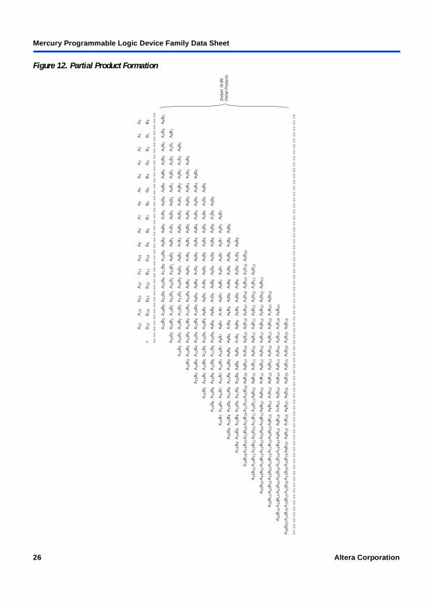
The basis for the high-speed 16 × 16-bit multiplier in a Mercury device is the binary tree multiplier. In the first stage of the binary tree, the multiplicand bits, a[15:0], and the multiplier bits, b[15:0], are multiplied together. The results of the first stage are sixteen 16-bit partial products, a[15:0]b[15], a[15:0]b[14], . . . a[15:0]b[0]. The partial products are then grouped into pairs and added together in the second stage. In a similar fashion, the results of the previous stage are grouped in pairs and then added forming the binary tree structure seen in Figure 12.
LAB Carry-In
Carry-In0
Carry-In1
Carry-Out0
Carry-Out1LAB Carry-Out
CLRN
D Q
ENA
RegisteredSum Output
CombinatorialSum Output
CombinatorialSum Output
ProgrammableInverter
ProgrammableInverter
AN
BM + 1
ProgrammableInverter
ProgrammableInverter
AN + 1
BM
FullAdder
LAB-Wide ClockEnable Signals (1)
Partial ProductGeneration
RapidLABInterconnect (2)
LE Output
LE Output
Altera Corporation 25
Mercury Programmable Logic Device Family Data Sheet
Figure 12. Partial Product Formation
A15
B0
A14
B1
A13
B2
A12
B3
A11
B4
A10
B5
A9B
6
A8B
7
A7B
8
A6B
9
A5B
10
A4B
11
A3B
12
A2B
13
A1B
14
A0B
15
A15
B1
A14
B2
A13
B3
A12
B4
A11
B5
A10
B6
A9B
7
A8B
8
A7B
9
A6B
10
A5B
11
A4B
12
A3B
13
A2B
14
A1B
15
A15
B2
A14
B3
A13
B4
A12
B5
A11
B6
A10
B7
A9B
8
A8B
9
A7B
10
A6B
11
A5B
12
A4B
13
A3B
14
A2B
15
A15
B3
A14
B4
A13
B5
A12
B6
A11
B7
A10
B8
A9B
9
A8B
10
A7B
11
A6B
12
A5B
13
A4B
14
A3B
15
A15
B4
A14
B5
A13
B6
A12
B7
A11
B8
A10
B9
A9B
10
A8B
11
A7B
12
A6B
13
A5B
14
A4B
15
A15
B5
A14
B6
A13
B7
A12
B8
A11
B9
A10
B10
A9B
11
A8B
12
A7B
13
A6B
14
A5B
15
A15
B6
A14
B7
A13
B8
A12
B9
A11
B10
A10
B11
A9B
12
A8B
13
A7B
14
A6B
15
A15
B7
A14
B8
A13
B9
A12
B10
A11
B11
A10
B12
A9B
13
A8B
14
A7B
15
A15
B8
A14
B9
A13
B10
A12
B11
A11
B12
A10
B13
A9B
14
A8B
15
A15
B9
A14
B10
A13
B11
A12
B12
A11
B13
A10
B14
A9B
15
A15
B10
A14
B11
A13
B12
A12
B13
A11
B14
A10
B15
A15
B11
A14
B12
A13
B13
A12
B14
A11
B15
A15
B12
A14
B13
A13
B14
A12
B15
A15
B13
A14
B14
A13
B15
A15
B14
A14
B15
A15
B15
A14
B0
A13
B1
A12
B2
A11
B3
A10
B4
A9B
5
A8B
6
A7B
7
A6B
8
A5B
9
A4B
10
A3B
11
A2B
12
A1B
13
A0B
14
A13
B0
A12
B1
A11
B2
A10
B3
A9B
4
A8B
5
A7B
6
A6B
7
A5B
8
A4B
9
A3B
10
A2B
11
A1B
12
A0B
13
A12
B0
A11
B1
A10
B2
A9B
3
A8B
4
A7B
5
A6B
6
A5B
7
A4B
8
A3B
9
A2B
10
A1B
11
A0B
12
A11
B0
A10
B1
A9B
2
A8B
3
A7B
4
A6B
5
A5B
6
A4B
7
A3B
8
A2B
9
A1B
10
A0B
11
A10
B0
A9B
1
A8B
2
A7B
3
A6B
4
A5B
5
A4B
6
A3B
7
A2B
8
A1B
9
A0B
10
A9B
0
A8B
1
A7B
2
A6B
3
A5B
4
A4B
5
A3B
6
A2B
7
A1B
8
A0B
9
A8B
0
A7B
1
A6B
2
A5B
3
A4B
4
A3B
5
A2B
6
A1B
7
A0B
8
A7B
0
A6B
1
A5B
2
A4B
3
A3B
4
A2B
5
A1B
6
A0B
7
A6B
0
A5B
1
A4B
2
A3B
3
A2B
4
A1B
5
A0B
6
A5B
0
A4B
1
A3B
2
A2B
3
A1B
4
A0B
5
A4B
0
A3B
1
A2B
2
A1B
3
A0B
4
A3B
0
A2B
1
A1B
2
A0B
3
A2B
0
A1B
1
A0B
2
A1B
0
A0B
1
A0B
0
A15
B15
A14
B14
A13
B13
A12
B12
A11
B11
A10
B10
A9
B9
A8
B8
A7
B7
A6
B6
A5
B5
A4
B4
A3
B3
A2
B2
A1
B1
A0
B0
==
==
==
==
==
==
==
==
==
==
==
==
==
==
==
==
==
==
==
==
==
==
==
==
==
==
==
==
==
==
==
==
==
==
==
==
==
==
==
==
==
==
==
==
==
==
==
==
==
==
==
==
==
==
==
==
==
==
==
==
==
==
==
==
==
==
==
==
==
==
==
==
==
==
==
==
==
==
==
==
==
==
==
==
==
==
==
==
==
==
==
==
==
==
==
==
==
==
==
==
==
==
==
==
==
==
==
==
==
==
×
Sixt
een
16-B
itPa
rtial
Pro
duct
s
26 Altera Corporation

Mercury Programmable Logic Device Family Data Sheet
Developm
ent
13
Tools
For a typical 16 × 16-bit binary tree multiplier, five stages are needed to determine the final product. The Mercury LE multiplier mode allows the partial product formation stage (Stage 1) and the first sum of stages (Stage 2) to be combined in a single stage, shown in Figure 13. This feature, combined with the direct connection between RapidLAB lines and LEs in multiplier mode, allows the fast dedicated implementation of multipliers.
Altera Corporation 27

Mercury Programmable Logic Device Family Data Sheet
Figure 13. Mercury Binary Tree Implementation
A[1
5:0]
B[1
5]A
[15:
0]B
[14]
A[1
5:0]
B[1
3]A
[15:
0]B
[12]
A[1
5:0]
B[1
1]A
[15:
0]B
[10]
A[1
5:0]
B[9
]A
[15:
0]B
[8]
A[1
5:0]
B[7
]A
[15:
0]B
[6]
A[1
5:0]
B[5
]A
[15:
0]B
[4]
A[1
5:0]
B[3
]A
[15:
0]B
[2]
A[1
5:0]
B[1
]A
[15:
0]B
[0]
+
+
+
+
++
++
++
+
+
++
+
Stag
e 1 St
age
2 Stag
e 3 St
age
4 Stag
e 5
Stag
es 1
and
2 a
reco
mbi
ned
into
one
leve
lof
LEs
28 Altera Corporation

Mercury Programmable Logic Device Family Data Sheet
Developm
ent
13
Tools
Clear & Preset Logic Control
LAB-wide signals control logic for the register’s clear and preset signals. The LE directly supports an asynchronous clear and preset function. The direct asynchronous preset does not require a NOT-gate push-back technique. Mercury devices support simultaneous preset, or asynchronous load, and clear. Asynchronous clear takes precedence if both signals are asserted simultaneously. Each LAB supports one clear and one preset signal. Two clears are possible in a single LAB by using a NOT-gate push-back technique on the preset port. The Quartus II Compiler automatically performs this second clear emulation.
In addition to the clear and preset ports, Mercury devices provide a chip-wide reset pin (DEV_CLRn) that resets all registers in the device. Use of this pin is controlled through an option in the Quartus II software that is set before compilation. The chip-wide reset overrides all other control signals.
Multi-Level FastTrack Interconnect
The Mercury architecture provides connections between LEs, ESBs, and device I/O pins via an innovative Multi-Level FastTrack Interconnect structure. The Multi-Level FastTrack Interconnect structure is a series of routing channels that traverse the device, providing a hierarchy of interconnect lines. Regular resources provide efficient and capable connections while priority resources and specialized RapidLAB, leap line, and FastLUT resources enhance performance by accelerating timing on critical paths. The Quartus II Compiler automatically places critical design paths on those faster lines to improve design performance.
This network of routing structures provides predictable performance, even for complex designs. In contrast, the segmented routing in FPGAs requires switch matrices to connect a variable number of routing paths, increasing the delays between logic resources and reducing performance.
The Multi-Level FastTrack Interconnect consists of regular and priority lines that traverse column and row interconnect channels to span sections and the entire device length. Each row of LABs, ESBs, and I/O bands is served by a dedicated row interconnect, which routes signals to and from LABs, ESBs, and I/O row bands in the same row. These row resources include:
Row interconnect traversing the entire device from left to right Priority row interconnect for high speed access across the length of
the device RapidLAB interconnect for horizontal routing that traverses a
10-LAB-wide region from a central LAB
Altera Corporation 29

Mercury Programmable Logic Device Family Data Sheet
The RapidLAB interconnect provides a specialized high-speed structure to allow a central LAB to drive other LABs within a 10-LAB-wide region. The RapidLAB lines drive alternating local LAB interconnect regions, allowing communication to all LABs in the 10-LAB-wide region. Even numbered LEs in a LAB directly drive a RapidLAB line that drives one set of alternating local interconnect regions, while odd-numbered LEs drive a RapidLAB line that drives the opposite set of alternating local interconnect regions. Figure 14 shows RapidLAB interconnect connections. This 10-LAB wide region of the RapidLAB interconnect is repeated for every LAB in the row. The region covered by the RapidLAB interconnect is smaller than 10 for source LABs that are four or five LABs in from either edge of the LAB row. The RapidLAB row interconnect is used for LAB-to-LAB routing; it is only used by I/O bands or ESBs indirectly through other interconnects. The RapidLAB interconnect drives an LE directly when that LE is in multiplier mode.
30 Altera Corporation

Mercury Programmable Logic Device Family Data Sheet
Developm
ent
13
Tools
Figure 14. RapidLAB Interconnect Connections
The column interconnect vertically routes signals to and from LABs, ESBs, and I/O bands. Each column of LABs is served by a dedicated column interconnect. These column resources include:
Column interconnect traversing the entire device from top to bottom Priority column interconnect for high speed access across the device
vertically Leap line interconnect for vertical routing between adjacent LAB
rows and between adjacent ESP rows and LAB rows.
Leap lines are driven directly by LEs for fast access to adjacent row interconnects. LABs can drive a leap line to the row above and/or below (including ESB rows). The even-numbered LEs in a LAB drive leap lines down, while odd-numbered LEs drive leap lines up. This allows a single LAB to access row and RapidLAB interconnects within a three-row region. Figure 15 shows the leap line interconnect.
LE 1
LE 3
LE 5
LE 7
LE 9
LE 2
LE 4
LE 6
LE 8
LE 10
RapidLAB Interconnect
Local InterconnectRapidLAB interconnects driven by odd-numberedLEs can drive out to the four LEs to the left and fiveLEs to the right through local interconnects.
RapidLAB interconnects driven by even-numberedLEs can drive out to the four LEs to the right and fiveLEs to the left through local interconnects.
LAB
Altera Corporation 31

Mercury Programmable Logic Device Family Data Sheet
Figure 15. Leap Line Interconnect
FastLUT Interconnect
Mercury devices include an enhanced interconnect structure within LABs for faster routing of LE output to LE input connections. The FastLUT connection allows the combinatorial output of an LE to directly drive the fast input of the LE directly below it, bypassing the local interconnect. This resource can be used as a high speed connection for wide fan-in functions from LE 1 to LE 10 in the same LAB. Figure 16 shows a FastLUT interconnect.
LAB Row n-1
LAB Row n
LAB Row n+1
Priority Rowand Row
RapidLAB
Leap Line
Leap Line
LE 10
LE 9
LE 8
LE 7
LE 6
LE 5
LE 4
LE 3
LE 2
LE 1
LE 10
LE 9
LE 8
LE 7
LE 6
LE 5
LE 4
LE 3
LE 2
LE 1
LE 10
LE 9
LE 8
LE 7
LE 6
LE 5
LE 4
LE 3
LE 2
LE 1
32 Altera Corporation

Mercury Programmable Logic Device Family Data Sheet
Developm
ent
13
Tools
Figure 16. FastLUT Interconnect
ESB rows also have their own interconnect resources to communicate horizontally and vertically with LAB rows. The ESB rows at the top and bottom of the device have their own set of row and priority row interconnect resources. For vertical communication, all LAB column interconnect lines traverse to the ESBs. This includes leap lines, which allow the adjacent LAB rows to communicate with the ESBs.
The row interconnect resources can be driven directly by LEs or ESBs in that row. Further, the column interconnect resources can drive a row line, allowing LEs, IOEs, and ESBs to drive elements in a different row via the column and row resources.
The column interconnect resources can be directly driven by LEs, IOEs, or ESBs within that column. The priority column and leap line resources can be driven directly by LEs. These lines enable high-speed vertical communication in the device for timing-critical paths. The column resources route signals between rows. A column resource can drive row resources directly, allowing fast connections between rows.
LE 1
LE 2
LE 3
LE 4
LE 5
LE 6
LE 7
LE 8
LE 9
LE 10
FastLUTRouting toAdjacent LE
Local InterconnectRouting Among LEsin the LAB
Altera Corporation 33

Mercury Programmable Logic Device Family Data Sheet
Table 9 summarizes how various elements of the Mercury architecture drive each other.
Notes to Table 9:(1) This direct connection is possible through the FastLUT connection.(2) IOEs can connect to the adjacent LAB’s local interconnects in the associated LAB row.(3) IOEs can connect to row and priority row interconnects in the associated LAB row.(4) This connection is used for multiplier mode.
Embedded System Block
The ESB can implement various types of memory blocks, including quad-port, true dual-port, dual- and single-port RAM, ROM, FIFO, and CAM blocks.
The ESB includes input and output registers; the input registers synchronize reads and/or writes, and the output registers can pipeline designs to further increase system performance. The ESB offers a quad port mode, which supports up to four port operations, two reads and two writes simultaneously, with the ability for a different clock on each of the four ports. Figure 17 shows the ESB quad-port block diagram.
Table 9. Mercury Routing Scheme
Source Destination
LE Local Interconnect
IOE ESB Row Interconnect
ESB Row Priority Row
RapidLAB Interconnect
Column Priority Column
Leap Lines
LE v (1)
v v v v v v v
Local Interconnect
v v
IOE v (2) v(3)
v (3) v v
ESB Row Interconnect
v
ESB v v v v
Row v
Priority Row v
RapidLAB Interconnect
v(4)
v
Column v v v v
Priority Column
v v v v v
Leap Lines v v v v v
34 Altera Corporation

Mercury Programmable Logic Device Family Data Sheet
Developm
ent
13
Tools
Figure 17. ESB Quad-Port Block Diagram
In addition to quad port memory, the ESB also supports true dual-port, dual-port, and single-port RAM. True dual-port RAM supports any combination of two port operations: two reads, two writes, or one read and one write. Dual-port memory supports a simultaneous read and write. For single-port memory, independent read and write is supported. Figure 18 shows these different RAM memory port configurations for an ESB.
dataA[ ]wraddressA[ ]wrenA
inclockA
inclockenA
inaclrA
rdaddressA[ ]rdenA
qA[ ] outclockA
outclockenA
outaclrA
dataB[ ]wraddressB[ ]
wrenB
inclockB inclockenB
inaclrB
rdaddressB[ ]rdenB
qB[ ]outclockB
outclockenB
outaclrB
A B
Altera Corporation 35

Mercury Programmable Logic Device Family Data Sheet
Figure 18. RAM Memory Port Configurations
Note to Figure 18:(1) Two dual- or single-port memory blocks can be implemented in a single ESB.
The ESB also allows variable width data ports for reading and writing to any of the RAM ports in any RAM configuration. For example, the ESB in quad port configuration can be written in ×1 mode at port A, read in ×16 from port A, written in ×4 mode at port B, and read in ×2 mode from port B.
dataA[ ]addressA[ ]wrenA
clockA
clockenA
qA[ ]aclrA
dataB[ ]addressB[ ]
wrenB
clockB clockenB
qB[ ]aclrB
A B
data[ ]wraddress[ ]wren inclockinclockeninaclr
rdaddress[ ]rden
q[ ]outclock outclocken
outaclr
data[ ]address[ ]wren inclockinclockeninaclr
q[ ]outclock outclocken
outaclr
True Dual-Port Memory
Single-Port Memory (1)
Dual-Port Memory (1)
36 Altera Corporation

Mercury Programmable Logic Device Family Data Sheet
Developm
ent
13
Tools
ESBs can implement synchronous RAM, which is easier to use than asynchronous RAM. A circuit using asynchronous RAM must generate the RAM write enable (WE) signal while ensuring that its data and address signals meet setup and hold time specifications relative to the WE signal. In contrast, the ESB’s synchronous RAM generates its own WE signal and is self-timed with respect to the global clock. Circuits using the ESB’s self-timed RAM must only meet the setup and hold time specifications relative to the global clock.
ESBs are grouped together in rows at the top and bottom of the device for fast horizontal communication. The ESB row interconnect can be driven by any ESB in the row. The row interconnect drives the ESB local interconnect, which in turn drives the ESB ports. ESB outputs drive the ESB local interconnect, which can drive row interconnect as well as all types of column interconnect, including leap lines. The leap lines allow fast access between ESBs and the adjacent LAB row.
When implementing memory, each ESB can be configured in any of the following sizes for quad port and true dual-port memory modes: 256 × 16; 512 × 8; 1,024 × 4; 2,048 × 2; or 4,096 × 1. For dual-port and single-port modes, the ESB can be configured for 128 × 32 in addition to the list above. For variable port width RAMs, any port width ratio combination must be 1, 2, 4, 8, or 16. For example, a RAM with data ports of width 1 and 16 or 2 and 32 will work, but not 1 and 32.
The ESB can also be split in half and used for two independent 2,048-bit single-port or dual-port RAM blocks. For example, one half of the ESB can be used as a 128 × 16 memory single-port memory while the other half can be used for a 1,024 × 2 dual-port memory. This effectively doubles the number of RAMs a Mercury device can implement for its given number of ESBs. The Quartus II software automatically merges two logical memory functions in a design into an ESB; the designer does not need to merge the functions manually.
By combining multiple ESBs, the Quartus II software implements larger memory blocks automatically. For example, two 256 × 16 RAM blocks can be combined to form a 256 × 32 RAM block, and two 512 × 8 RAM blocks can be combined to form a 512 × 16 RAM block. Memory performance does not degrade for memory blocks up to 4,096 words deep. Each ESB can implement a 4,096-word-deep memory; the ESBs are used in parallel, eliminating the need for any external control logic and its associated delays. To create a high-speed memory block more than 4,096 words deep, the Quartus II software will automatically combine ESBs with LE control logic.
Altera Corporation 37

Mercury Programmable Logic Device Family Data Sheet
The ESB implements two forms of clocking modes for quad-port and dual-port memory—read/write clock mode and input/output clock mode.
Read/Write Clock Mode
An ESB implementing quad-port memory in read/write clock mode can use up to four clocks. For port A, one clock controls all registers associated with writing: data input, WE, and write address. The other clock controls all registers associated with reading: read enable (RE), read address, and data output. Another set of clocks can be used for port B of the RAM, or the same clocks can be used. Each ESB port, A or B, also supports independent read clock enable, write clock enable, and asynchronous clear signals. Read/write clock mode is commonly used for applications where reads and writes occur at different system frequencies. Figure 19 shows the ESB in read/write clock mode.
38 Altera Corporation

Mercury Programmable Logic Device Family Data Sheet
Developm
ent
13
Tools
Figure 19. ESB in Read/Write Clock Mode Notes (1), (2)
Notes to Figure 19:(1) Only half of the ESB, either A or B, is used for dual-port configuration.(2) All registers can be asynchronously cleared by ESB local interconnect signals, global signals, or the chip-wide reset.(3) This configuration is supported for dual-port configuration.
Fou
r D
edic
ated
Clo
cks
46
D EN
A
Q
D EN
A
Q
D EN
A
Q
D EN
A
Q
D EN
A
Q
data
A[]
rda
ddre
ssA[]
wra
ddre
ssA[]
RA
M/R
OM
128
× 32
(3)
256
× 16
512
× 8
1,02
4 ×
42,
048
× 2
4,09
6 ×
1
Dat
a In
Rea
d A
ddre
ss
Writ
e A
ddre
ss
Rea
d E
nabl
e
Writ
e E
nabl
e
Dat
a O
ut[]
Dat
a In
Rea
d A
ddre
ss
Writ
e A
ddre
ss
Rea
d E
nabl
e
Writ
e E
nabl
e
Dat
a O
ut[]
outc
lken
A
incl
ken A
incl
ock A
outc
lock
A
D EN
A
Q
Writ
eP
ulse
Gen
erat
or
rden
A
wre
n A
Six
Ded
icat
ed In
puts
& G
loba
l Sig
nals
q A[]
46
EN
A
data
B[]
rda
ddre
ssB[]
wra
ddre
ssB[]
outc
lken
B
incl
ken B
incl
ock B
outc
lock
B
Writ
eP
ulse
Gen
erat
or
rden
B
wre
n B
q B[]
EN
A
EN
A
EN
A
D
EN
A
Q
EN
A
AB
DQ
DQ
DQ
DQ
DQ
Altera Corporation 39

Mercury Programmable Logic Device Family Data Sheet
Input/Output Clock Mode
An ESB using input/output clock mode can also use up to four clocks. On each of the two ports, A or B, one clock controls all registers for inputs into the ESB: data input, WE, RE, read address, and write address. The other clock controls the ESB data output registers. Each ESB port, A or B, also supports independent read clock enable, write clock enable, and asynchronous clear signals. Input/output clock mode is commonly used for applications where the reads and writes occur at the same system frequency, but require different clock enable signals for the input and output registers. Figure 20 shows the ESB in input/output clock mode.
40 Altera Corporation

Mercury Programmable Logic Device Family Data Sheet
Developm
ent
13
Tools
Figure 20. ESB in Input/Output Clock Mode Notes (1), (2)
Notes to Figure 20:(1) Only half of the ESB, either A or B, is used for dual-port configuration.(2) All registers can be asynchronously cleared by ESB local interconnect signals, global signals, or the chip-wide reset.(3) This configuration is supported for dual-port configuration.
Fou
r D
edic
ated
Clo
cks
46
D EN
A
Q
D EN
A
Q
D EN
A
Q
D EN
A
Q
D EN
A
Q
data
A[ ]
rda
ddre
ssA[ ]
wra
ddre
ssA[ ]
RA
M/R
OM
128
× 32
(3)
256
× 16
512
× 8
1,02
4 ×
42,
048
× 2
4,09
6 ×
1
Dat
a In
Rea
d A
ddre
ss
Writ
e A
ddre
ss
Rea
d E
nabl
e
Writ
e E
nabl
e
Dat
a O
ut[]
Dat
a In
Rea
d A
ddre
ss
Writ
e A
ddre
ss
Rea
d E
nabl
e
Writ
e E
nabl
e
Dat
a O
ut[]
outc
lken
A
incl
ken A
incl
ock A
outc
lock
A
D EN
A
Q
Writ
eP
ulse
Gen
erat
or
rden
A
wre
n A
Six
Ded
icat
ed In
puts
& G
loba
l Sig
nals
q A[]
46
EN
A
data
B[ ]
rda
ddre
ssB[ ]
wra
ddre
ssB[ ]
outc
lken
B
incl
ken B
incl
ock B
outc
lock
B
Writ
eP
ulse
Gen
erat
or
rden
B
wre
n B
q B[]
EN
A
EN
A
EN
A
EN
A
EN
A
AB
DQ
DQ
DQ
DQ
DQ
DQ
Altera Corporation 41

Mercury Programmable Logic Device Family Data Sheet
Single-Port Mode
The Mercury device’s ESB also supports a single-port mode, which is used when simultaneous reads and writes are not required. See Figure 21. A single ESB can support up to two single-port mode RAMs.
Figure 21. ESB in Single-Port Mode Note (1)
Notes to Figure 21:(1) All registers can be asynchronously cleared by ESB local interconnect signals, global signals, or chip-wide reset.(2) If there is only one single-port RAM block in an ESB, it can support the following configurations: 4,096 × 1; 2,048 × 2;
1,028 × 4; 512 × 8; 256 × 16; or 128 × 32.
Content-Addressable Memory
Mercury devices can implement CAM in ESBs. CAM can be thought of as the inverse of RAM. RAM stores data in a specific location; when the system submits an address, the RAM block provides the data. Conversely, when the system submits data to CAM, the CAM block provides the address where the data is found. For example, if the data FA12 is stored in address 14, the CAM outputs 14 when FA12 is driven into it.
Dedicated Clocks
4 6
D
ENA
Q
D
ENA
Q
D
ENA
Q
D
ENA
Q
data[ ]
address[ ]
RAM/ROM (2)128 × 16
256 × 8512 × 4
1,024 × 22,048 × 1
Data In
Address
Write Enable
Data Out
outclken
inclken
inclock
outclock
WritePulse
Generator
wren
Dedicated FastGlobal Signals
To FastTrackInterconnect
42 Altera Corporation

Mercury Programmable Logic Device Family Data Sheet
Developm
ent
13
Tools
CAM is used for high-speed search operations. When searching for data within a RAM block, the search is performed serially. Thus, finding a particular data word can take many cycles. CAM searches all addresses in parallel and outputs the address storing a particular word. When a match is found, a match flag is set high. CAM is ideally suited for applications such as Ethernet address lookup, data compression, pattern recognition, cache tags, fast routing table lookup, and high-bandwidth address filtering. Figure 22 shows the CAM block diagram.
Figure 22. CAM Block Diagram
The Mercury on-chip CAM provides faster system performance than traditional discrete CAM. Integrating CAM and logic into the Mercury device eliminates off-chip and on-chip delays, improving system performance.
When in CAM mode, the ESB implements a 32-word, 32-bit CAM. Wider or deeper CAM, such as a 32-word, 64-bit or 128-word, 32-bit block, can be implemented by combining multiple CAM blocks with some ancillary logic implemented in LEs. The Quartus II software automatically combines ESBs and LEs to create larger CAM blocks.
CAM supports writing “don’t care” bits into words of the memory. The don’t-care bit can be used as a mask for CAM comparisons; any bit set to don’t-care has no effect on matches.
CAM can generate outputs in three different modes: single-match mode, multiple-match mode, and fast multiple-match mode. In each mode, the ESB outputs the matched data’s location as an encoded or unencoded address. When encoded, the ESB outputs an encoded address of the data’s location. For instance, if the data is located in address 12, the ESB output is 12. When unencoded, each ESB port uses its 16 outputs to show the location of the data over two clock cycles. In this case, if the data is located in address 12, the 12th output line goes high. Figures 22 and 23 show the encoded CAM outputs and unencoded CAM outputs, respectively.
data[ ]wraddress[ ]wren inclockinclockeninaclr
data_address[ ]match
outclock outclocken
outaclr
Altera Corporation 43

Mercury Programmable Logic Device Family Data Sheet
Figure 23. Encoded CAM Address Outputs
Figure 24. Unencoded CAM Address Outputs
Notes to Figure 24:(1) For an unencoded output, the ESB only supports 31 input data bits. One input bit
is used by the select line to choose one of the two banks of 16 outputs.(2) If the select input is a 1, then CAM outputs odd words between 1 through 15. If
the select input is a 0, CAM outputs words even words between 0 through 14.
In single-match mode, it takes two clock cycles to write into CAM, but only one clock cycle to read from CAM. In this mode, both encoded and unencoded outputs are available without external logic. Single-match mode is better suited for designs without duplicate data in the memory.
CAM
data[31..0] = 45
addr[15..0] = 12Encoded Output
match = 1
AddressData
10111213
15274585
CAM
data[30..0] =45 (1)
select (2)
q0
Unencoded outputs.q12 goes high tosignify a match.
q12
q13
q14
q15
AddressData
10111213
15274585
44 Altera Corporation

Mercury Programmable Logic Device Family Data Sheet
Developm
ent
13
Tools
If the same data is written into multiple locations in the memory, a CAM block can be used in multiple-match or fast multiple-match modes. The ESB outputs the matched data’s locations as an encoded or unencoded address. In multiple-match mode, it takes two clock cycles to write into a CAM block. For reading, there are 16 outputs from each ESB at each clock cycle. Therefore, it takes two clock cycles to represent the 32 words from a single ESB port. In this mode, encoded and unencoded outputs are available. To implement the encoded version, the Quartus II software adds a priority encoder with LEs. Fast multiple-match is identical to the multiple-match mode, however, it only takes one clock cycle to read from a CAM block and generate valid outputs. To do this, the entire ESB is used to represent 16 outputs. In fast multiple-match mode, the ESB can implement a maximum CAM block size of 16 words.
A CAM block can be pre-loaded with data during configuration, or it can be written during system operation. In most cases, two clock cycles are required to write each word into CAM. When don’t-care bits are used, a third clock cycle is required.
f For more information on CAM, see Application Note 119 (Implementing High-Speed Search Applications with APEX CAM).
Driving into ESBs
ESBs provide flexible options for driving control signals. Different clocks can be used for the ESB inputs and outputs. Registers can be inserted independently on the data input, data output, read address, write address, WREN, and RDEN signals on each port of the ESB. The fast global signals and ESB local interconnect can drive the WREN and RDEN signals. The fast global signals, dedicated clock pins, and ESB local interconnect can drive the ESB clock signals. The ESB local interconnect is driven by the ESB row interconnects which, in turn, are driven by all types of column interconnects, including high-speed leap lines. Because the LEs drive the column interconnect to the ESB local interconnect, the LEs can control the WREN and RDEN signals and the ESB clock, clock enable, and asynchronous clear signals. Figure 25 shows the ESB control signal generation logic.
Altera Corporation 45

Mercury Programmable Logic Device Family Data Sheet
Figure 25. ESB Control Signal Generation
The ESB can drive row interconnects within its own ESB row and can directly drive all the column interconnects: column, priority column, and leap lines.
Implementing Logic in ROM
In addition to implementing RAM functions, the ESB can implement logic functions when it is programmed with a read-only pattern during configuration, creating a large LUT. With LUTs, combinatorial functions are implemented by looking up the results, rather than by computing them. This implementation of combinatorial functions can be faster than using algorithms implemented in general logic, a performance advantage further enhanced by the fast access times of ESBs. The large capacity of ESBs enables designers to implement complex functions in one logic level without the routing delays associated with linked LEs or distributed RAM blocks. Parameterized functions such as LPM functions can take advantage of the ESB automatically. Further, the Quartus II software can implement portions of a design with ESBs where appropriate.
INCLOCK
INCLOCKEN
OUTCLOCK
OUTCLOCKEN
DedicatedClocks
Fast GlobalSignals
LocalInterconnect
LocalInterconnect
LocalInterconnect
LocalInterconnect
4
6
LocalInterconnect
LocalInterconnect
WREN
INCLR
OUTCLR
RDEN
46 Altera Corporation

Mercury Programmable Logic Device Family Data Sheet
Developm
ent
13
Tools
Programmable Speed/Power Control
Mercury device ESBs offer the Turbo BitTM option, a high-speed mode that supports fast operation on an ESB-by-ESB basis. When high speed is not required, the Turbo Bit option can be turned off to reduce power dissipation by up to 50%. ESBs that run at low power incur a nominal timing delay adder. An ESB that is not used will be powered down so it does not consume DC current.
Designers can program each ESB in the Mercury device for either high-speed or low-power operation. As a result, speed-critical paths in the design can run at high speed, while the remaining paths operate at reduced power.
I/O Structure The IOE in Mercury devices contains a bidirectional I/O buffer and three registers for a complete embedded bidirectional IOE. The IOE contains individual input, output, and output enable registers. The input register can be used for external data requiring fast setup times. The output register can be used for data requiring fast clock-to-output performance. The output enable (OE) register can be used for fast clock-to-output enable timing. The Quartus II software automatically duplicates a single OE register that controls multiple output or bidirectional pins.
For normal bidirectional operation, the input register can have its own clock input separate from the OE and output registers. The OE and output register share the same clock source. Each register can have its own clock enable signal from local interconnect in the associated LAB, fast global signals, or row global signals.
Altera Corporation 47
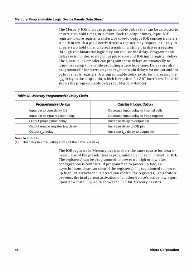
Mercury Programmable Logic Device Family Data Sheet
The Mercury IOE includes programmable delays that can be activated to ensure zero hold times, minimum clock-to-output times, input IOE register-to-core register transfers, or core-to-output IOE register transfers. A path in which a pin directly drives a register may require the delay to ensure zero hold time, whereas a path in which a pin drives a register through combinatorial logic may not require the delay. Programmable delays exist for decreasing input pin to core and IOE input register delays. The Quartus II Compiler can program these delays automatically to minimize setup time while providing a zero hold time. Delays are also programmable for increasing the register to pin delays for output and/or output enable registers. A programmable delay exists for increasing the tZX delay to the output pin, which is required for ZBT interfaces. Table 10 shows the programmable delays for Mercury devices.
Note to Table 10:(1) This delay has four settings: off and three levels of delay.
The IOE registers in Mercury devices share the same source for clear or preset. Use of the preset/clear is programmable for each individual IOE. The register(s) can be programmed to power up high or low after configuration is complete. If programmed to power up low, an asynchronous clear can control the register(s). If programmed to power up high, an asynchronous preset can control the register(s). This feature prevents the inadvertent activation of another device’s active-low input upon power-up. Figure 26 shows the IOE for Mercury devices.
Table 10. Mercury Programmable Delay Chain
Programmable Delays Quartus II Logic Option
Input pin to core delay (1) Decrease input delay to internal cells
Input pin to input register delay Decrease input delay to input register
Output propagation delay Increase delay to output pin
Output enable register tCO delay Increase delay to OE pin
Output tZX delay Increase tZX delay to output pin
48 Altera Corporation

Mercury Programmable Logic Device Family Data Sheet
Developm
ent
13
Tools
Figure 26. Mercury IOE
Note to Figure 26:(1) This programmable delay has four settings: off and three levels of delay.
Double Data Rate I/O
Mercury device’s have three register IOEs to support the DDRIO feature, which makes double data rate interfaces possible by clocking data on both positive and negative clock edges. The IOE in Mercury devices supports double data rate input and double data rate output modes.
CLRN/PRN
D Q
ENA
Chip-Wide Reset
OE Register
CLRN/PRN
D Q
ENA
CLRN/PRN
D Q
ENA
Output Register
Input Register
Output tZXDelay
OE RegistertCO Delay
OutputPropagation Delay
Input Pin toCore Delay (1)
Drive Strength Control
Open-Drain OutputSlew Control
Input Pin to Input Register Delay
VCCIO
VCCIO
OptionalPCI Clamp
ProgrammablePull-Up
Priority Row Interconnect (for Associated LAB Row)
Row Interconnect (for Associated LAB Row)
Column andPriorityColumn
Interconnect
Associated LABLocal Interconnect
Two RowLocal Fast
Signals
Six FastGlobalSignals
Four Dedicated
Clocks
Bus-HoldCircuit
Altera Corporation 49
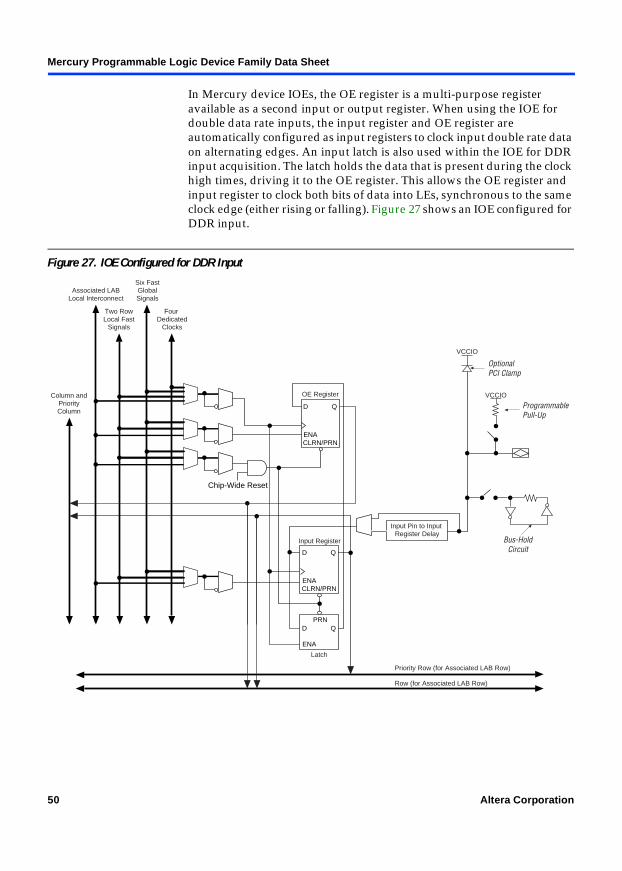
Mercury Programmable Logic Device Family Data Sheet
In Mercury device IOEs, the OE register is a multi-purpose register available as a second input or output register. When using the IOE for double data rate inputs, the input register and OE register are automatically configured as input registers to clock input double rate data on alternating edges. An input latch is also used within the IOE for DDR input acquisition. The latch holds the data that is present during the clock high times, driving it to the OE register. This allows the OE register and input register to clock both bits of data into LEs, synchronous to the same clock edge (either rising or falling). Figure 27 shows an IOE configured for DDR input.
Figure 27. IOE Configured for DDR Input
CLRN/PRN
D Q
ENA
Chip-Wide Reset
OE Register
CLRN/PRN
D Q
ENA
PRND Q
ENA
Input Register
Input Pin to Input Register Delay
VCCIO
VCCIO
OptionalPCI Clamp
ProgrammablePull-Up
Priority Row (for Associated LAB Row)
Row (for Associated LAB Row)
Column andPriorityColumn
Associated LABLocal Interconnect
Two RowLocal Fast
Signals
Six FastGlobalSignals
Four Dedicated
Clocks
Bus-HoldCircuit
Latch
50 Altera Corporation

Mercury Programmable Logic Device Family Data Sheet
Developm
ent
13
Tools
When using the IOE for double data rate outputs, the output register and OE register are automatically configured to clock two data paths from LEs on rising clock edges. These register outputs are multiplexed by the clock to drive the output pin at a ×2 rate. The output register clocks the first bit out on the clock high time, while the OE register clocks the second bit out on the clock low time. Figure 28 shows the IOE configured for DDR output.
Figure 28. IOE Configured for DDR Output
Bidirectional DDR on an I/O pin is possible by using the IOE for DDR output and using LEs to acquire the double data rate input. Bidirectional DDR I/O pins support double data rate synchronous DRAM (DDR SDRAM) at 166 MHz (334 Mbps), which transfer data on a double data rate bidirectional bus. QDR SRAMs are also supported with DDR I/O pins on separate read and write ports.
CLRN/PRN
D Q
ENA
Chip-Wide Reset
OE Register
CLRN/PRN
D Q
ENA
Output Register Output Propagation Delay
Drive Strength Control
Open-Drain OutputSlew Control
VCCIO
VCCIO
OptionalPCI Clamp
ProgrammablePull-Up
Associated LABLocal Interconnect
Two RowLocal Fast
Signals
Six FastGlobalSignals
Four Dedicated
Clocks
Bus-HoldCircuit
01
Altera Corporation 51
Mercury Programmable Logic Device Family Data Sheet
Zero Bus Turnaround SRAM Interface Support
In addition to DDR SDRAM support, Mercury device I/O pins also support interfacing with ZBT SRAM blocks at up to 200 MHz. ZBT SRAM blocks are designed to eliminate dead bus cycles when turning a bidirectional bus around between reads and writes, or writes and reads. ZBT allows for 100% bus utilization because ZBT SRAM can read or write on every clock cycle.
To avoid bus contention, the output tZX delay ensures that the clock-to-low-impedance time (tZX) is greater than the clock-to-high-impedance time (tXZ). Time delay control of clocks to the OE/output and input register, using a single general purpose PLL, enable the Mercury device to meet ZBT tCO and tSU times.
Programmable Drive Strength
The output buffer for each Mercury device I/O pin has a programmable drive strength control for certain I/O standards. The LVTTL standard has several levels of drive strength that can be controlled by the user. SSTL-3 class I and II, SSTL-2 class I and II, HSTL class I and II, and 3.3-V GTL+ support a minimum or maximum setting. The minimum setting is the lowest drive strength that guarantees the IOH/IOL of the standard. The maximum setting provides higher drive strength that allows for faster switching and is the default setting. Using settings below the maximum provides signal slew-rate control to reduce system noise and signal overshoot. Table 11 shows the possible settings for the I/O standards with drive strength control.
52 Altera Corporation

Mercury Programmable Logic Device Family Data Sheet
Developm
ent
13
Tools
Open-Drain Output
Mercury devices provide an optional open-drain (equivalent to an open-collector) output for each I/O pin. This open-drain output enables the device to provide system-level control signals (e.g., interrupt and write enable signals) that can be asserted by any of several devices.
Slew-Rate Control
The output buffer for each Mercury device I/O pin has a programmable output slew rate control that can be configured for low-noise or high-speed performance. A faster slew rate provides high-speed transitions for high-performance systems. However, these fast transitions may introduce noise transients into the system. A slow slew rate reduces system noise, but adds a nominal delay to rising and falling edges. Each I/O pin has an individual slew rate control, allowing the designer to specify the slew rate on a pin-by-pin basis. The slew rate control affects both the rising and falling edges.
Table 11. Programmable Drive Strength
I/O Standard IOH/IOL Current StrengthSetting
LVTTL (3.3 V) 4 mA
8 mA
12 mA
16 mA
24 mA (default)
LVTTL (2.5 V) 4 mA
8 mA
12 mA
16 mA (default)
LVTTL (1.8 V) 2 mA
4 mA (default)
SSTL-3 class I and IISSTL-2 class I and IIHSTL class I and IIGTL+ (3.3 V)
Minimum
Maximum (default)
Altera Corporation 53

Mercury Programmable Logic Device Family Data Sheet
Bus Hold
Each Mercury device I/O pin provides an optional bus-hold feature. When this feature is enabled for an I/O pin, the bus-hold circuitry weakly holds the signal at its last driven state. By holding the last driven state of the pin until the next input signal is present, the bus-hold feature eliminates the need to add external pull-up or pull-down resistors to hold a signal level when the bus is tri-stated. The bus-hold circuitry also pulls undriven pins away from the input threshold voltage where noise can cause unintended high-frequency switching. This feature can be selected individually for each I/O pin. The bus-hold output will drive no higher than VCCIO to prevent overdriving signals. If the bus-hold feature is enabled, the programmable pull-up option cannot be used. The bus-hold feature should also be disabled if open-drain outputs are used with the GTL+ I/O standard.
The bus-hold circuitry weakly pulls the signal level to the last driven state through a resistor with a nominal resistance (RBH) of approximately 8 kΩ. Table 42 gives specific sustaining current that will be driven through this resistor and overdrive current that will identify the next driven input level. This information is provided for each VCCIO voltage level.
The bus-hold circuitry is active only after configuration. When going into user mode, the bus-hold circuit captures the value on the pin present at the end of configuration.
Programmable Pull-Up Resistor
Each Mercury device I/O pin provides an optional programmable pull-up resistor during user mode. When this feature is enabled for an I/O pin, the pull-up resistor (50 kΩ) weakly holds the output to the VCCIO level of the bank that the output pin resides in.
I/O Row Bands
The I/O row bands are one of the advanced features of the Mercury architecture. All IOEs are grouped in I/O row bands across the device. The number of I/O row bands depends on the Mercury device size. The I/O row bands are designed for flip-chip technology, allowing I/O pins to be distributed across the entire chip, not only in the periphery. This array driver technology allows higher I/O pin density (I/O pins per device area) than peripheral I/O pins.
54 Altera Corporation

Mercury Programmable Logic Device Family Data Sheet
Developm
ent
13
Tools
Each row of I/O pins has an associated LAB row for driving to and from the core of the Mercury device. For a given I/O band row, its associated LAB row is located below it with the exception of the bottom I/O band row. The bottom I/O band is located at the bottom periphery of the device, hence its associated LAB row is located above it. Figure 29 shows an example of an I/O band to associated LAB row interconnect in a Mercury device.
There is a maximum of two IOEs associated with each LAB in the associated LAB row. The local interconnect of the associated LAB drives the IOEs. Since local interconnect is shared with the LAB neighbor, any given LAB can directly drive up to four IOEs. The local interconnect drives the data and OE signals when the IOE is used as an output or bidirectional pin.
Figure 29. IOE Connection to Interconnects and Adjacent LAB Note (1)
Note to Figure 29:(1) INA: unregistered input; INB: registered/unregistered input; INC: registered/unregistered input or OE register
output in DDR mode.
The IOEs drive registered or combinatorial versions of input data into the device. The unregistered input data can be driven to the local interconnect (for fast input setup), row and priority row interconnect, and column and priority column interconnects. The registered data can also be driven to the same row and column resources. The OE register output can be fed back through column and row interconnects to implement DDR I/O pins.
LAB LAB LAB
I/O BandRow
AssociatedLAB Row
IOE Pair
INA
INC
INB OUT INA
INC
INB OUT
Row Interconnect
Priority Row Interconnect
All Column Interconnects
Associated LABto IOE Pair Local Interconnect
IOE pairs drive unregistered inputs to the associated LAB's local interconnect.
The associated LAB and its neighbor can drive a given IOE pair through the local interconnect.
IOEIOE
IOE Pair
INA
INC
INB OUT INA
INC
INB OUT
IOEIOE
IOE Pair
INA
INC
INB OUT INA
INC
INB OUT
IOEIOE
To LocalInterconnect
To NextLAB
Altera Corporation 55

Mercury Programmable Logic Device Family Data Sheet
Dedicated Fast Lines & I/O Pins
Mercury devices incorporate dedicated bidirectional pins for signals with high internal fanout, such as PCI control signals. These pins are called dedicated fast I/O pins (FAST1, FAST2, FAST3, FAST4, FAST5, and FAST6) and can drive the six global fast lines throughout the device, ideal for fast clock, clock enable, clear, preset, or high fanout logic signal distribution. The dedicated fast I/O pins have the same IOE as a regular I/O pin. The dedicated fast lines can also be driven by a LE local interconnect to generate internal global signals.
In addition to the device global fast lines, each LAB row has two dedicated fast lines local to the row. This is ideal for high fanout control signals for a section of a design that may fit into a single LAB row. Each I/O band (with the exception of the top I/O band) has two dedicated row-global fast I/O pins to drive the row-global fast resources for the associated LAB. The dedicated local fast I/O pins have the same IOE as a regular I/O pin. The LE local interconnect can drive dedicated row-global fast lines to generate internal global signals specific to a row. There are no pin connections for buried LAB rows; LE local interconnects drive the row-global signals in those rows.
I/O Standard Support
Mercury device IOEs support the following I/O standards:
LVTTL LVCMOS 1.8-V 2.5-V 3.3-V PCI 3.3-V PCI-X 3.3-V AGP (1×, 2×) LVDS LVPECL 3.3-V PCML GTL+ HSTL class I and II SSTL-3 class I and II SSTL-2 class I and II CTT
56 Altera Corporation

Mercury Programmable Logic Device Family Data Sheet
Developm
ent
13
Tools
Table 12 describes the I/O standards supported by Mercury devices.
Each regular I/O band row contains two I/O banks. The number of I/O banks in a Mercury device depends on the number of I/O band rows. The top I/O band contains four regular I/O banks specifically designed for HSDI. The top I/O band banks and dedicated clock inputs support LVDS, LVPECL, and 3.3-V PCML. 3.3-V PCML is an open-drain standard and therefore requires external termination to 3.3 V. All other standards are supported by all I/O banks. The top I/O banks 1, 2, 3, and 4 only support non-HSDI I/O pins if the design does not use HSDI circuitry. If the design uses any HSDI channel, banks 1, 2, 3, and 4 all do not support regular I/O pins.
Additionally, the EP1M350 device includes the Flexible-LVDS feature, providing support for up to 100 LVDS channels on all regular I/O banks. Regular I/O banks in EP1M350 devices include dedicated LVDS input and output buffers that do not require any external components except for 100-Ω termination resistors on receiver channels.
Table 12. Mercury Supported I/O Standards
I/O Standard Type Input Reference
Voltage (VREF) (V)
OutputSupplyVoltage
(VCCIO) (V)
Board Termination
Voltage(VTT) (V)
LVTTL Single-ended N/A 3.3 N/A
LVCMOS Single-ended N/A 3.3 N/A
2.5 V Single-ended N/A 2.5 N/A
1.8 V Single-ended N/A 1.8 N/A
3.3-V PCI Single-ended N/A 3.3 N/A
3.3-V PCI-X Single-ended N/A 3.3 N/A
LVDS Differential N/A 3.3 N/A
LVPECL Differential N/A 3.3 N/A
3.3-V PCML Differential N/A 3.3 3.3
GTL+ Voltage referenced 1.0 N/A 1.5
HSTL class I and II Voltage referenced 0.75 1.5 0.75
SSTL-2 class I and II Voltage referenced 1.25 2.5 1.25
SSTL-3 class I and II Voltage referenced 1.5 3.3 1.5
AGP Voltage referenced 1.32 3.3 N/A
CTT Voltage referenced 1.5 3.3 1.5
Altera Corporation 57

Mercury Programmable Logic Device Family Data Sheet
For the HSDI I/O band, half of the dedicated banks support LVDS, 3.3-V PCML or LVPECL, and receiver inputs, while the other half support LVDS, PCML or LVPECL, and transmitter outputs. A single device can support 1.5-V, 1.8-V, 2.5-V, and 3.3-V interfaces; each bank can support a VCCIO standard independently. Each bank can also use a separate VREF level so that each bank can support any of the terminated standards (such as SSTL-3) independently. A bank can support a single VREF level. Each bank contains a fixed VREF pin for voltage referenced standards. This pin can be used as a regular I/O if a VREF standard is not used. Table 13 shows the number of I/O banks in each Mercury device.
Each bank can support multiple standards with the same VCCIO for output pins. For EP1M120 devices, each bank can support one voltage-referenced I/O standard, but can support multiple I/O standards with the same VCCIO and VREF voltage levels. For example, when VCCIO is 3.3 V, a bank can support LVTTL, LVCMOS, 3.3-V PCI, and SSTL-3 for inputs and outputs. Figure 30 shows the I/O bank layout for an EP1M120 device. For EP1M350 devices, each bank can support two voltage-reverenced I/O standards; each I/O bank is split into two voltage-referenced sub-banks. When using the two HSDI transmitter banks as regular I/O banks in a non-HSDI mode, those two banks require the same VCCIO level. However, each HSDI transmitter bank supports its own VREF level.
Table 13. Number of I/O Banks per Device
Device Regular I/O Banks HSDI Band I/O Banks
EP1M120 8 4
EP1M350 12 4
58 Altera Corporation

Mercury Programmable Logic Device Family Data Sheet
Developm
ent
13
Tools
Figure 30. I/O Bank Layout
Notes to Figure 30:(1) If HSDI I/O channels are not used, the HSDI banks can be used as regular I/O banks.(2) When used as regular I/O banks, these banks must be set to the same VCCIO level, but can have separate VREF bank
settings.
f For more information on I/O standards, see Application Note 117 (Using Selectable I/O Standards in Altera Devices).
MultiVolt I/O Interface
The Mercury architecture supports the MultiVolt I/O interface feature, which allows Mercury devices in all packages to interface with devices with different supply voltages. The devices have one set of VCC pins for internal operation and input buffers (VCCINT), and another set for I/O output drivers (VCCIO).
Input, Output, or HSDI Transmitter (1), (2)Input, Output, or HSDI Receiver (1)
Input, Output, or HSDI Transmitter (1), (2)Input, Output, or HSDI Receiver (1)
I/O Bank
ESB ESB ESB ESB ESB ESB
ESB ESB ESB ESB ESB ESB
I/O or HSDIBanks
Regular I/OBanks
I/O Bank
I/O Bank
I/O Bank
I/O Bank
I/O Bank
I/O Bank
I/O Bank
Altera Corporation 59

Mercury Programmable Logic Device Family Data Sheet
The Mercury VCCINT pins must always be connected to a 1.8-V power supply. With a 1.8-V VCCINT level, input pins are 1.8-V, 2.5-V and 3.3-V tolerant. The VCCIO pins can be connected to either a 1.5-V, 1.8-V, 2.5-V or 3.3-V power supply, depending on the output requirements. When VCCIO pins are connected to a 1.5-V power supply, the output levels are compatible with HSTL systems. When VCCIO pins are connected to a 1.8-V power supply, the output levels are compatible with 1.8-V systems. When VCCIO pins are connected to a 2.5-V power supply, the output levels are compatible with 2.5-V systems. When the VCCIO pins are connected to a 3.3-V power supply, the output high is 3.3 V and is compatible with 3.3-V or 5.0-V systems.
Table 14 summarizes Mercury MultiVolt I/O support.
Notes to Table 14:(1) The PCI clamping diode must be disabled to drive an input with voltages higher than VCCIO unless an external
resistor is used.(2) These input levels are only available if the input standard is set to any VREF-based input standard (SSTL-2, SSTL-3,
HSTL, GTL+, AGP 2×). The input buffers are powered from VCCINT when using VREF-based input standards. LVTTL, PCI, PCI-X, AGP 1× input buffers are powered by VCCIO. Therefore, these standards cannot be driven with input levels below the VCCIO setting except for when VCCIO = 3.3 V and the input voltage (VI) = 2.5 V.
(3) When VCCIO = 1.8 V, the Mercury device can drive a 1.5-V device with 1.8-V tolerant inputs.(4) When VCCIO = 2.5 V, the Mercury device can drive a 1.8-V device with 2.5-V tolerant inputs.(5) When VCCIO = 3.3 V, the Mercury device can drive a 2.5-V device with 3.3-V tolerant inputs.(6) Designers can set Mercury devices to be 5.0-V tolerant by adding an external resistor and enabling the PCI clamping
diode.
Power Sequencing & Hot-Socketing
Because Mercury devices can be used in a mixed-voltage environment, the devices are designed specifically to tolerate any possible power-up sequence. Therefore, the VCCIO and VCCINT power supplies may be powered in any order.
Signals can be driven into Mercury devices before and during power-up without damaging the device. In addition, Mercury devices do not drive out during power-up. Once operating conditions are reached and the device is configured, Mercury devices operate as specified by the user.
Table 14. Mercury MultiVolt I/O Support Note (1)
VCCIO (V)
Input Signal Output Signal
1.5 V 1.8 V 2.5 V 3.3 V 5.0 V 1.5 V 1.8 V 2.5 V 3.3 V 5.0 V
1.5 v v v v v
1.8 v (2) v v v v (3)
2.5 v (2) v (2) v v v (4) v
3.3 v (2) v (2) v (2) v v (6) v (5) v v
60 Altera Corporation

Mercury Programmable Logic Device Family Data Sheet
Developm
ent
13
Tools
General Purpose PLL
Mercury devices have ClockLockTM, ClockBoostTM, and advanced ClockShiftTM features, which use up to four general-purpose PLLs (separate from the two HSDI PLLs) to province clock management and clock-frequency synthesis. EP1M120 devices contain two general purpose PLLs; EP1M350 devices contain four general purpose PLLs. These PLLs allow designers to increase performance and provide clock-frequency synthesis. The PLL reduces the clock delay within a device. This reduction minimizes clock-to-output and setup times while maintaining zero hold times. The PLLs, which provide programmable multiplication, allow the designer to distribute a low-speed clock and multiply that clock on-device. Mercury devices include a high-speed clock tree: unlike ASICs, the user does not have to design and optimize the clock tree. The PLLs work in conjunction with the Mercury device’s high-speed clock to provide significant improvements in system performance and bandwidth. Table 15 shows the general purpose PLL features for Mercury devices. Figure 31 shows a Mercury PLL.
Note to Table 15:(1) n represents the prescale divider for the PLL input. k, p, q, and v represent the different post scale dividers for the
four possible PLL outputs. m, k, p, and q are integers that range from 1 to 160. n and v are integers that can range from 1 to 16.
Figure 31. Mercury General-Purpose PLL
Table 15. Mercury General Purpose PLL Features
Device Number of PLLs ClockBoost Feature (1)
Number of External Clock Outputs
Number of Feedback Inputs
Advanced ClockShift
EP1M120 2 m/(n × k, p, q, v) 2 2 v
EP1M350 4 m/(n × k, p, q, v) 4 4 v
m
n
kTime
Delay/Shift
TimeDelay/Shift
TimeDelay/Shift
TimeDelay/Shift
p
q
v
PhaseComparator Voltage-Controlled
Oscillator
inclock
fbin
clock1
clock0
clock2
clock_ext
ClockLock
Phase ShiftCircuitry
Altera Corporation 61

Mercury Programmable Logic Device Family Data Sheet
The PLLs in Mercury devices are enabled through the Quartus II software. External devices are not required to use these features.
Advanced ClockBoost Multiplication & Division
Each Mercury PLL includes circuitry that provides clock synthesis for up to four outputs (three internal outputs and one external output) using m/(n × output divider) scaling. When a PLL is locked, the locked output clock aligns to the rising edge of the input clock. The closed loop equation for Figure 31 gives an output frequency fclock0 = (m/(n × k))fIN, fclock1 = (m/(n × p))fIN, fclock2 = (m/(n × q))fIN, and fclock_ext = (m/(n × v))fIN or fclock1. These equations allow the multiplication or division of clocks by a programmable number. The Quartus II software automatically chooses the appropriate scaling factors according to the frequency, multiplication, and division values entered.
A single PLL in a Mercury device allows for multiple user-defined multiplication and division ratios that are not possible even with multiple delay-locked loops (DLLs). For example, if a frequency scaling factor of 3.75 is needed for a given input clock, a multiplication factor of 15 and a division factor of 4 can be entered. This advanced multiplication scaling can be performed with a single PLL, making it unnecessary to cascade PLL outputs.
External Clock Outputs
Mercury devices have four low-jitter external clocks available for external clock sources. Other devices on the board can use these outputs as clock sources.
There are three modes for external clock outputs. Multiplication is allowed in all external clock output modes.
Zero Delay Buffer: The external clock output pin is phase aligned with the clock input pin for zero delay. Programmable phase shift and time delay shift are not allowed in this configuration. Multiplication is allowed with the zero delay buffer mode. The MegaWizard interface for altclklock should be used to verify possible clock settings.
External Feedback: The external feedback input pin is phase aligned with clock input pin. By aligning these clocks, you can actively remove clock delay and skew between devices. Multiplication is allowed with the external feedback mode. This mode has the same restrictions as zero delay buffer mode.
62 Altera Corporation

Mercury Programmable Logic Device Family Data Sheet
Developm
ent
13
Tools
Normal Mode: The external clock output pin will have phase delay relative to the clock input pin. If an internal clock is used in this mode, the IOE register clock will be phase aligned to the input clock pin. Multiplication is allowed with the normal mode.
Advanced ClockShift Circuitry
General purpose PLLs in Mercury devices have advanced ClockShiftTM circuitry that provides programmable phase shift and fine tune time delay shift. For phase shifting, users can enter a phase shift (in degrees or time units) that affects all PLL outputs. Phase shifts of 90, 180, and 270 can be implemented exactly. Other values of phase shifting, or delay shifting in time units, are allowed with a resolution range of 0.3 ns to 1.0 ns. This resolution varies with frequency input and the user-entered multiplication and division factors. The phase shift ability is only possible on a multiplied or divided clock if the input and output frequency have an integer multiple relationship (i.e., fIN/fOUT or fOUT/fIN must be an integer).
In addition to the phase shift feature that affects all outputs, there is an advanced fine time delay shift control on each of the four PLL outputs. Each PLL output can be shifted in 250-ps increments for a range of –2.0 ns to +2.0 ns. This ability can be used in conjunction with the phase shifting ability that affects all outputs. fIN/fOUT does not need to have an integer relationship for the advanced fine time delay shift control.
Clock Enable Signal
Mercury PLLs have a CLKLK_ENA pin for enabling/disabling all of the device PLLs. When the CLKLK_ENA pin is high, the PLL drives a clock to all its output ports. When the CLKLK_ENA pin is low, the clock0, clock1, clock2 and extclock ports are driven by GND and all of the PLLs go out of lock. When the CLKLK_ENA pin goes high again, the PLL must relock.
The individual enable port for each general purpose PLL is programmable. If more than one general-purpose PLL is instantiated, each one does not have to use the clock enable. To enable/disable the device PLLs with the CLKLK_ENA pin, the inclocken port on the altclklock instance must be connected to the CLKLK_ENA input pin.
Altera Corporation 63

Mercury Programmable Logic Device Family Data Sheet
Lock Signals
The Mercury device general purpose PLL circuits support individual LOCK signals. The LOCK signal drives high when the PLL has locked onto the input clock. Lock remains high as long as the input remains within specification. It will go low if the input is out of specification. A LOCK pin is optional for each PLL used in the Mercury devices; when not used, they are I/O pins. This signal is not available internally; if it is used in the core, it must be fed back in with an input pin.
SignalTap Embedded Logic Analyzer
Mercury devices include device enhancements to support the SignalTap embedded logic analyzer. By including this circuitry, the Mercury device provides the ability to monitor design operation over a period of time through the IEEE Std. 1149.1 JTAG circuitry; a designer can analyze internal logic at speed without bringing internal signals to the I/O pins. This feature is particularly important for advanced packages such as FineLine BGA packages, because it can be difficult to add a connection to a pin during the debugging process after a board is designed and manufactured.
IEEE Std. 1149.1 (JTAG) Boundary-Scan Support
All Mercury devices provide JTAG BST circuitry that complies with the IEEE Std. 1149.1-1990 specification. JTAG boundary-scan testing can be performed before or after configuration, but not during configuration. Mercury devices can also use the JTAG port for configuration with the Quartus II software or with hardware using either Jam Standard Test and Programming Language (STAPL) Files (.jam) or Jam STAPL Byte-Code Files (.jbc). Mercury devices also use the JTAG port to monitor the logic operation of the device with the SignalTap embedded logic analyzer. Mercury devices support the JTAG instructions shown in Table 16.
64 Altera Corporation

Mercury Programmable Logic Device Family Data Sheet
Developm
ent
13
Tools
The Mercury device instruction register length is 10 bits. The Mercury device USERCODE register length is 32 bits. Tables 17 and 18 show the boundary-scan register length and device IDCODE information for Mercury devices.
Notes to Table 18:(1) The most significant bit (MSB) is on the left.(2) The IDCODE’s least significant bit (LSB) is always 1.
Table 16. Mercury JTAG Instructions
JTAG Instruction Description
SAMPLE/PRELOAD Allows a snapshot of signals at the device pins to be captured and examined during normal device operation and permits an initial data pattern to be output at the device pins. Also used by the SignalTap embedded logic analyzer.
EXTEST Allows the external circuitry and board-level interconnections to be tested by forcing a test pattern at the output pins and capturing test results at the input pins.
BYPASS Places the 1-bit bypass register between the TDI and TDO pins, which allows the BST data to pass synchronously through selected devices to adjacent devices during normal device operation.
USERCODE Selects the 32-bit USERCODE register and places it between the TDI and TDO pins, allowing the USERCODE to be serially shifted out of TDO.
IDCODE Selects the IDCODE register and places it between TDI and TDO, allowing the IDCODE to be serially shifted out of TDO.
ICR Instructions These instructions are used when configuring a Mercury device via the JTAG port with a ByteBlasterMVTM download cable, or using a Jam STAPL or Jam Byte-Code file via an embedded processor.
SignalTap Instructions
These instructions monitor internal device operation with the SignalTap embedded logic analyzer.
Table 17. Mercury Boundary-Scan Register Length
Device Boundary-Scan Register Length (Bits)
EP1M120 1,125
EP1M350 1,695
Table 18. 32-Bit Mercury Device IDCODE
Device IDCODE (32 Bits) (1)
Version (4 Bits)
Part Number (16 Bits) Manufacturer Identity (11 Bits)
1 (1 Bit) (2)
EP1M120 0000 0011 0000 0000 0000 000 0110 1110 1
EP1M350 0000 0011 0000 0000 0001 000 0110 1110 1
Altera Corporation 65

Mercury Programmable Logic Device Family Data Sheet
Figure 32 shows the timing requirements for the JTAG signals.
Figure 32. Mercury JTAG Waveforms
Table 19 shows the JTAG timing parameters and values for Mercury devices.
Table 19. Mercury JTAG Timing Parameters & Values
Symbol Parameter Min Max Unit
tJCP TCK clock period 100 ns
tJCH TCK clock high time 50 ns
tJCL TCK clock low time 50 ns
tJPSU JTAG port setup time 20 ns
tJPH JTAG port hold time 45 ns
tJPCO JTAG port clock to output 25 ns
tJPZX JTAG port high impedance to valid output 25 ns
tJPXZ JTAG port valid output to high impedance 25 ns
tJSSU Capture register setup time 20 ns
tJSH Capture register hold time 45 ns
tJSCO Update register clock to output 35 ns
tJSZX Update register high impedance to valid output 35 ns
tJSXZ Update register valid output to high impedance 35 ns
TDO
TCK
tJPZX tJPCO
tJPH
t JPXZ
tJCP
tJPSU t JCL tJCH
TDI
TMS
Signalto Be
Captured
Signalto Be
Driven
tJSZX
tJSSU tJSH
tJSCO tJSXZ
66 Altera Corporation

Mercury Programmable Logic Device Family Data Sheet
Developm
ent
13
Tools
f For more information, see the following documents:
Application Note 39 (IEEE Std. 1149.1 (JTAG) Boundary-Scan Testing in Altera Devices)
Jam Programming & Test Language Specification
Generic Testing Each Mercury device is functionally tested. Complete testing of each configurable static random access memory (SRAM) bit and all logic functionality ensures 100% yield. AC test measurements for Mercury devices are made under conditions equivalent to those shown in Figure 33. Multiple test patterns can be used to configure devices during all stages of the production flow.
Altera Corporation 67

Mercury Programmable Logic Device Family Data Sheet
Figure 33. Mercury AC Test Conditions
Operating Conditions
Table 20 through 43 provide information on absolute maximum ratings, recommended operating conditions, DC operating conditions, and capacitance for 1.8-V Mercury devices.
System
C1 (includesjig capacitance)Device input
rise and falltimes < 3 ns
DeviceOutput
To Test
Power supply transients can affect AC measurements. Simultaneous transitions of multiple outputs should be avoided for accurate measurement. Threshold tests must not be performed under AC conditions. Large-amplitude, fast-ground-current transients normally occur as the device outputs discharge the load capacitances. When these transients flow through the parasitic inductance between the device ground pin and the test system ground, significant reductions in observable noise immunity can result.
Table 20. Mercury Device Absolute Maximum Ratings Note (1)
Symbol Parameter Conditions Minimum Maximum Unit
VCCINT Supply voltage With respect to ground (2) –0.5 2.5 V
VCCIO –0.5 4.6 V
VI DC input voltage –0.5 4.6 V
IOUT DC output current, per pin –34 34 mA
TSTG Storage temperature No bias –65 150 ° CTAMB Ambient temperature Under bias –65 135 ° CTJ Junction temperature BGA packages under bias 135 ° C
68 Altera Corporation

Mercury Programmable Logic Device Family Data Sheet
Developm
ent
13
Tools
Table 21. Mercury Device Recommended Operating Conditions
Symbol Parameter Conditions Minimum Maximum Unit
VCCINT Supply voltage for internal logic and input buffers
(3) 1.71 1.89 V
VCCIO Supply voltage for output buffers, 3.3-V operation
(3), (4) 3.00 (3.135) 3.60 (3.465) V
Supply voltage for output buffers, 2.5-V operation
(3) 2.375 2.625 V
Supply voltage for output buffers, 1.8-V operation
(3) 1.71 1.89 V
Supply voltage for output buffers, 1.5-V operation
(3) 1.4 1.6 V
VI Input voltage (2), (5) –0.5 4.1 V
VO Output voltage 0 VCCIO V
TJ Operating temperature For commercial use
0 85 ° C
For industrial use –40 100 ° CtR Input rise time 40 ns
tF Input fall time 40 ns
Table 22. Mercury Device DC Operating Conditions Note (6), (7)
Symbol Parameter Conditions Minimum Typical Maximum Unit
II Input pin leakage current
VI = VCCIOmax to 0 V (5) –10 10 µA
IOZ Tri-stated I/O pin leakage current
VO = VCCIOmax to 0 V (5) –10 10 µA
ICC0 VCC supply current (standby) for EP1M120 devices
For commercial use (8) 30 mA
For Industrial use (8) 40 mA
VCC supply current (standby) for EP1M350 devices
For commercial use (8) 50 mA
For Industrial use (8) 60 mA
RCONF Value of I/O pin pull-up resistor before and during configuration
VCCIO = 3.0 V (9) 20 50 kΩVCCIO = 2.375 V (9) 30 80 kΩVCCIO = 1.71 V (9) 60 150 kΩ
Altera Corporation 69

Mercury Programmable Logic Device Family Data Sheet
Table 23. LVTTL Specifications Note (10)
Symbol Parameter Conditions Minimum Maximum Units
VCCIO Output supply voltage 3.0 3.6 V
VIH High-level input voltage 1.7 4.1 V
VIL Low-level input voltage –0.5 0.7 V
II Input pin leakage current VIN = 0 V or VCCIO –10 10 µA
VOH High-level output voltage IOH = –4 mA 2.4 V
VOL Low-level output voltage IOL = 4 mA 0.45 V
Table 24. LVCMOS Specifications
Symbol Parameter Conditions Minimum Maximum Units
VCCIO Power supply voltage range 3.0 3.6 V
VIH High-level input voltage 1.7 4.1 V
VIL Low-level input voltage –0.5 0.7 V
II Input pin leakage current VIN = 0 V or VCCIO –10 10 µA
VOH High-level output voltage VCCIO = 3.0, IOH = –0.1 mA
VCCIO – 0.2 V
VOL Low-level output voltage VCCIO = 3.0,IOL = 0.1 mA
0.2 V
Table 25. 2.5-V I/O Specifications Note (10)
Symbol Parameter Conditions Minimum Maximum Units
VCCIO Output supply voltage 2.375 2.625 V
VIH High-level input voltage 1.7 4.1 V
VIL Low-level input voltage –0.5 0.7 V
II Input pin leakage current VIN = 0 V or VCCIO 10 10 µA
VOH High-level output voltage IOH = –0.1 mA 2.1 V
IOH = –1 mA 2.0 V
IOH = –2 mA 1.7 V
VOL Low-level output voltage IOL = 0.1 mA 0.2 V
IOH = 1 mA 0.4 V
IOH = 2 mA 0.7 V
70 Altera Corporation

Mercury Programmable Logic Device Family Data Sheet
Developm
ent
13
Tools
Figures 34 and 35 show receiver input and transmitter output waveforms, respectively, for all differential I/O standards (LVPECL, 3.3-V PCML, LVDS, and HyperTransport technology).
Figure 34. Receiver Input Waveforms for Differential I/O Standards
Table 26. 1.8-V I/O Specifications Note (10)
Symbol Parameter Conditions Minimum Maximum Units
VCCIO Output supply voltage 1.71 1.89 V
VI H High-level input voltage 0.65 × VCCIO 4.1 V
VIL Low-level input voltage –0.5 0.35 × VCCIO V
II Input pin leakage current VIN = 0 V or VCCIO –10 10 µA
VOH High-level output voltage IOH = –2 mA VCCIO – 0.45 V
VOL Low-level output voltage IOL = 2 mA 0.45 V
Single-Ended Waveform
Differential Waveform
Positive Channel (p) = VIH
Negative Channel (n) = VIL
Ground
±VID
+VID
− VIDVID (Peak-to-Peak)
VCM
p − n = 0 V
Altera Corporation 71

Mercury Programmable Logic Device Family Data Sheet
Figure 35. Transmitter Output Waveforms for Differential I/O StandardsSingle-Ended Waveform
Differential Waveform
Positive Channel (p) = VOH
Negative Channel (n) = VOL
Ground
±VOD
+VOD
− VODVOD (Peak-to-Peak)
p − n = 0 V
VCM
Table 27. 3.3-V LVDS I/O Specifications
Symbol Parameter Conditions Minimum Typical Maximum Units
VCCIO I/O supply voltage 3.135 3.3 3.465 V
VOD Differential output voltage RL = 100 Ω 250 510 600 mV
∆ VOD Change in VOD between high and low
RL = 100 Ω 50 mV
VOS Output offset voltage RL = 100 Ω 1.125 1.25 1.375 V
∆ VOS Change in VOS between high and low
RL = 100 Ω 50 mV
VTH Differential input threshold VCM = 1.2 V –100 100 mV
VIN Receiver input voltage range
0.0 2.4 V
RL Receiver differential input resistor (external to Mercury devices)
90 100 110 Ω
72 Altera Corporation

Mercury Programmable Logic Device Family Data Sheet
Developm
ent
13
Tools
Table 28. 3.3-V PCML Specifications
Symbol Parameter Conditions Minimum Typical Maximum Units
VCCIO I/O supply voltage 3.135 3.3 3.465 V
VIL Low-level input voltage VCCIO – 0.4
V
VIH High-level input voltage VCCIO V
VOL Low-level output voltage VCCIO – 0.4
V
VOH High-level output voltage VCCIO V
VT Output termination voltage VCCIO V
VID Differential input voltage 400 800 mV
VOD Differential output voltage 400 700 800 mV
tR Rise time (20 to 80%) 200 ps
tF Fall time (20 to 80%) 200 ps
tDSKEW Differential skew 25 ps
R1 (11) Output load 90 100 110 ΩR2 (11) Receiver differential input
resistor45 50 55 Ω
Table 29. LVPECL Specifications
Symbol Parameter Conditions Minimum Typical Maximum Units
VCCIO I/O supply voltage 3.135 3.3 3.465 V
VIL Low-level input voltage 0 2,000 mV
VIH High-level input voltage 400 2,470 mV
VOL Low-level output voltage 1,400 1,650 mV
VOH High-level output voltage 2,275 2,470 mV
VID Differential input voltage 400 600 1,200 mV
VOD Differential output voltage 525 1,050 1,200 mV
tR Rise time (20 to 80%) 85 325 ps
tF Fall time (20 to 80%) 85 325 ps
tDSKEW Differential skew 25 ps
RL Receiver differential input resistor
100 Ω
Altera Corporation 73

Mercury Programmable Logic Device Family Data Sheet
Table 30. 3.3-V PCI Specifications
Symbol Parameter Conditions Minimum Typical Maximum Units
VCCIO I/O supply voltage 3.0 3.3 3.6 V
VIH High-level input voltage 0.5 × VCCIO
VCCIO + 0.5
V
VIL Low-level input voltage –0.5 0.3 × VCCIO
V
II Input pin leakage current 0 < VIN < VCCIO –10 10 µA
VOH High-level output voltage IOUT = –500 µA 0.9 × VCCIO
V
VOL Low-level output voltage IOUT = 1,500 µA 0.1 × VCCIO
V
Table 31. PCI-X Specifications
Symbol Parameter Conditions Minimum Typical Maximum Units
VCCIO I/O supply voltage 3.0 3.6 V
VIH High-level input voltage 0.5 × VCCIO
VCCIO + 0.5
V
VIL Low-level input voltage –0.5 0.35 × VCCIO
V
VIPU Input pull-up voltage 0.7 × VCCIO
V
IIL Input leakage current 0 < VIN < VCCIO –10 10 µA
VOH High-level output voltage IOUT = –500 µA 0.9 × VCCIO
V
VOL Low-level output voltage IOUT = 1,500 µA 0.1 × VCCIO
V
LPIN Pin inductance 15 nH
Table 32. GTL+ I/O Specifications Note (10)
Symbol Parameter Conditions Minimum Typical Maximum Units
VTT Termination voltage 1.35 1.5 1.65 V
VREF Reference voltage 0.88 1.0 1.12 V
VIH High-level input voltage VREF + 0.1 V
VIL Low-level input voltage VREF – 0.1 V
VOL Low-level output voltage IOL = 34 mA 0.65 V
74 Altera Corporation

Mercury Programmable Logic Device Family Data Sheet
Developm
ent
13
Tools
Table 33. SSTL-2 Class I Specifications Note (10)
Symbol Parameter Conditions Minimum Typical Maximum Units
VCCIO I/O supply voltage 2.375 2.5 2.625 V
VTT Termination voltage VREF – 0.04 VREF VREF + 0.04 V
VREF Reference voltage 1.15 1.25 1.35 V
VIH High-level input voltage VREF + 0.18 3.0 V
VIL Low-level input voltage –0.3 VREF – 0.18 V
VOH High-level output voltage IOH = –7.6 mA VTT + 0.57 V
VOL Low-level output voltage IOL = 7.6 mA VTT – 0.57 V
Table 34. SSTL-2 Class II Specifications Note (10)
Symbol Parameter Conditions Minimum Typical Maximum Units
VCCIO I/O supply voltage 2.3 2.5 2.7 V
VTT Termination voltage VREF – 0.04 VREF VREF + 0.04 V
VREF Reference voltage 1.15 1.25 1.35 V
VIH High-level input voltage VREF + 0.18 VCCIO + 0.3 V
VIL Low-level input voltage –0.3 VREF – 0.18 V
VOH High-level output voltage IOH = –15.2 mA VTT + 0.76 V
VOL Low-level output voltage IOL = 15.2 mA VTT – 0.76 V
Table 35. SSTL-3 Class I Specifications Note (10)
Symbol Parameter Conditions Minimum Typical Maximum Units
VCCIO I/O supply voltage 3.0 3.3 3.6 V
VTT Termination voltage VREF – 0.05 VREF VREF + 0.05 V
VREF Reference voltage 1.3 1.5 1.7 V
VIH High-level input voltage VREF + 0.2 VCCIO + 0.3 V
VIL Low-level input voltage –0.3 VREF – 0.2 V
VOH High-level output voltage IOH = –8 mA VTT + 0.6 V
VOL Low-level output voltage IOL = 8 mA VTT – 0.6 V
Altera Corporation 75

Mercury Programmable Logic Device Family Data Sheet
Table 36. SSTL-3 Class II Specifications Note (10)
Symbol Parameter Conditions Minimum Typical Maximum Units
VCCIO I/O supply voltage 3.0 3.3 3.6 V
VTT Termination voltage VREF – 0.05 VREF VREF + 0.05 V
VREF Reference voltage 1.3 1.5 1.7 V
VIH High-level input voltage VREF + 0.2 VCCIO + 0.3 V
VIL Low-level input voltage –0.3 VREF – 0.2 V
VOH High-level output voltage IOH = –16 mA VT T + 0.8 V
VOL Low-level output voltage IOL = 16 mA VTT – 0.8 V
Table 37. 3.3-V AGP -2X Specifications
Symbol Parameter Conditions Minimum Typical Maximum Units
VCCIO I/O supply voltage 3.15 3.3 3.45 V
VREF Reference voltage 0.39 × VCCIO 0.41 × VCCIO V
VIH High-level input voltage (12)
0.5 × VCCIO VCCIO + 0.5 V
VIL Low-level input voltage (12)
0.3 × VCCIO V
VOH High-level output voltage IOUT = –20 µA 0.9 × VCCIO 3.6 V
VOL Low-level output voltage IOUT = 20 µA 0.1 × VCCIO V
II Input pin leakage current 0 < VIN < VCCIO ±10 µA
Table 38. 3.3-V AGP -1X Specifications
Symbol Parameter Conditions Minimum Typical Maximum Units
VCCIO I/O supply voltage 3.15 3.3 3.45 V
VIH High-level input voltage (12)
0.5 × VCCIO VCCIO + 0.5 V
VIL Low-level input voltage (12)
0.3 × VCCIO V
VOH High-level output voltage IOUT = –20 µA 0.9 × VCCIO 3.6 V
VOL Low-level output voltage IOUT = 20 µA 0.1 × VCCIO V
II Input pin leakage current 0 < VIN < VCCIO ±10 µA
76 Altera Corporation

Mercury Programmable Logic Device Family Data Sheet
Developm
ent
13
Tools
Table 39. 1.5-V HSTL Class I Specifications Note (10)
Symbol Parameter Conditions Minimum Typical Maximum Units
VCCIO I/O supply voltage 1.4 1.5 1.6 V
VREF Input reference voltage 0.68 0.75 0.9 V
VTT Termination voltage 0.7 0.75 0.8 V
VIH (DC) DC high-level input voltage VREF + 0.1 V
VIL (DC) DC low-level input voltage –0.3 VREF – 0.1 V
VIH (AC) AC high-level input voltage VREF + 0.2 V
VIL (AC) AC low-level input voltage VREF – 0.2 V
VOH High-level output voltage IOH = 8 mA VCCIO – 0.4 V
VOL Low-level output voltage IOH = –8 mA 0.4 V
Table 40. 1.5-V HSTL Class II Specifications Note (10)
Symbol Parameter Conditions Minimum Typical Maximum Units
VCCIO I/O supply voltage 1.4 1.5 1.6 V
VREF Input reference voltage 0.68 0.75 0.9 V
VTT Termination voltage 0.7 0.75 0.8 V
VIH (DC) DC high-level input voltage VREF + 0.1 V
VIL (DC) DC low-level input voltage –0.3 VREF – 0.1 V
VIH (AC) AC high-level input voltage VREF + 0.2 V
VIL (AC) AC low-level input voltage VREF – 0.2 V
VOH High-level output voltage IOH = 16 mA VCCIO – 0.4 V
VOL Low-level output voltage IOH = –16 mA 0.4 V
Table 41. CTT I/O Specifications
Symbol Parameter Conditions Minimum Typical Maximum Units
VCCIO I/O supply voltage 3.0 3.3 3.6 V
VTT/VREF Termination and input reference voltage
1.35 1.5 1.65 V
VIH High-level input voltage VREF + 0.2 V
VIL Low-level input voltage VREF – 0.2 V
II Input pin leakage current 0 < VIN < VCCIO ±10 µA
VOH High-level output voltage IOH = –8 mA VREF + 0.4 V
VOL Low-level output voltage IOL = 8 mA VREF – 0.4 V
IO Output leakage current (when output is high Z)
GND ð VOUT ð VCCIO
±10 µA
Altera Corporation 77

Mercury Programmable Logic Device Family Data Sheet
Table 42. Bus Hold Parameters
Parameter Conditions VCCIO Level Units
1.8 V 2.5 V 3.3 V
Minimum Maximum Minimum Maximum Minimum Maximum
Low sustaining current
VIN > VIL (maximum)
30 50 70 µA
High sustaining current
VIN < VIH (minimum)
–30 –50 –70 µA
Low overdrive current
0 V < VIN < VCCIO
200 300 500 µA
High overdrive current
0 V < VIN < VCCIO
–200 –300 –500 µA
Table 43. Mercury Device Capacitance Note (13)
Symbol Parameter Minimum Typical Maximum Unit
CIO I/O pin capacitance 13.5 pF
CCLK Input capacitance on CLK[4..1] pins 16.9 pF
CRXHSDI Input capacitance on HSDI receiver pins 8.0 pF
CTXHSDI Input capacitance on HSDI transmitter pins 18.0 pF
CCLKHSDI Input capacitance on HSDI clock pins 7.5 pF
CFLEXLVDSRX Input capacitance on flexible LVDS receiver pins
13.4 pF
CFLEXLVDSTX Input capacitance on flexible LVDS transmitter pins
13.4 pF
78 Altera Corporation

Mercury Programmable Logic Device Family Data Sheet
Developm
ent
13
Tools
Notes to Tables 20 – 43.:(1) See the Operating Requirements for Altera Devices Data Sheet.(2) Minimum DC input is –0.5 V. During transitions, the inputs may undershoot to –0.5 V or overshoot to 4.1 V for input
currents less than 100 mA and periods shorter than 20 ns.(3) Maximum VCC rise time is 100 ms, and VCC must rise monotonically.(4) VCCIO maximum and minimum conditions for LVPECL, LVDS, RapidIO, and 3.3-V PCML are shown in
parentheses.(5) All pins, including dedicated inputs, clock, I/O, and JTAG pins, may be driven before VCCINT and VCCIO are
powered.(6) Typical values are for TA = 25° C, VCCINT = 1.8 V, and VCCIO = 1.8 V, 2.5 V, and 3.3 V.(7) These values are specified under the Mercury Device Recommended Operating Conditions shown in Table 3 on
page 3.(8) Input pins are grounded. In the test design, internal logic does not toggle. The test design does not use PLL or HSDI
circuitry. All ESBs are in power-down mode.(9) Pin pull-up resistance values will lower if an external source drives the pin higher than VCCIO.(10) Drive strength is programmable according to values in Table 11 on page 53.(11) For more information on termination, see AN 134: Using Programmable I/O Standards in Mercury Devices or
AN 159: Using HSDI in Source-Synchronous Mode in Mercury Devices.(12) VREF specifies the center point of the switching range.(13) Capacitance is sample-tested only. Capacitance is measured using time-domain reflections (TDR). Measurement
accuracy is within ±5%.
Timing Model The high-performance multi-level FastTrack Interconnect routing resources ensure predictable performance, accurate simulation, and accurate timing analysis. The predictable performance of Mercury devices offer an advantage over FPGAs, which use a segmented connection scheme and therefore have unpredictable performance.
Figure 36 shows the timing model for bidirectional IOE pin timing. All registers are within the IOE.
Figure 36. Synchronous Bidirectional Pin External Timing Model
PRN
CLRN
D Q
PRN
CLRN
D Q
PRN
CLRN
D Q
DedicatedClock
BidirectionalPin
Output Register
Input Register
OE Register
tINSUBIDIR
tOUTCOBIDIR
tXZBIDIRtZXBIDIR
tINHBIDIR
Altera Corporation 79

Mercury Programmable Logic Device Family Data Sheet
Tables 44 and 45 describe the Mercury device’s external timing parameters.
Notes to Tables 44 and 45:(1) These timing parameters are sample-tested only.(2) All timing parameters are either to and/or from pins, including global clock pins.
Table 44. Mercury External Timing Parameters Notes (1), (2)
Symbol Parameter Conditions
tINSU Setup time with global clock at IOE register
tINH Hold time with global clock at IOE register
tOUTCO Clock-to-output delay with global clock at IOE register C1 = 35 pF
tINSUPLL Setup time with PLL clock at IOE input register
tINHPLL Hold time with PLL clock at IOE input register
tOUTCOPLL Clock-to-output delay with PLL clock at IOE output register C1 = 35 pF
Table 45. Mercury External Bidirectional Timing Parameters Notes (1), (2)
Symbol Parameter Conditions
tINSUBIDIR Setup time for bidirectional pins with gobal clock at IOE input register
tINHBIDIR Hold time for bidirectional pins with global clock at IOE input register
tOUTCOBIDIR Clock-to-output delay for bidirectional pins with global clock at IOE output register
C1 = 35 pF
tXZBIDIR Synchronous IOE output enable register to output buffer disable delay C1 = 35 pF
tZXBIDIR Synchronous IOE output enable register output buffer enable delay C1 = 35 pF
tINSUBIDIRPLL Setup time for bidirectional pins with PLL clock at IOE input register
tINHBIDIRPLL Hold time for bidirectional pins with PLL clock at IOE input register
tOUTCOBIDIRPLL Clock-to-output delay for bidirectional pins with PLL clock at IOE output register
C1 = 35 pF
tXZBIDIRPLL Synchronous IOE output enable register to output buffer disable delay with PLL
C1 = 35 pF
tZXBIDIRPLL Synchronous IOE output enable register output buffer enable delay with PLL
C1 = 35 pF
80 Altera Corporation

Mercury Programmable Logic Device Family Data Sheet
Developm
ent
13
Tools
Tables 46 through 51 show external timing parameters for Mercury devices.
Table 46. EP1M120 External Timing Parameters Note (1)
Symbol -5 Speed Grade -6 Speed Grade -7 Speed Grade Unit
Min Max Min Max Min Max
tINSU 0.67 0.70 0.73 ns
tINH 0.00 0.00 0.00 ns
tOUTCO 2.00 3.30 2.00 3.32 2.00 3.49 ns
tINSUPLL 0.59 0.64 0.62 ns
tINHPLL 0.00 0.00 0.00 ns
tOUTCOPLL 0.50 2.08 0.50 2.08 0.50 2.15 ns
Table 47. EP1M120 External Bidirectional Timing Parameters Note (1)
Symbol -5 Speed Grade -6 Speed Grade -7 Speed Grade Unit
Min Max Min Max Min Max
tINSUBIDIR 0.67 0.70 0.73 ns
tINHBIDIR 0.00 0.00 0.00 ns
tOUTCOBIDIR 2.00 3.30 2.00 3.32 2.00 3.49 ns
tXZBIDIR 3.52 3.53 3.74 ns
tZXBIDIR (2) 3.52 3.53 3.74 ns
tZXBIDIR (3) 3.72 3.73 3.99 ns
tINSUBIDIRPLL 0.59 0.64 0.62 ns
tINHBIDIRPLL 0.00 0.00 0.00 ns
tOUTCOBIDIRPLL 0.50 2.08 0.50 2.08 0.50 2.15 ns
tXZBIDIRPLL 2.29 2.29 2.39 ns
tZXBIDIRPLL (2) 2.29 2.29 2.39 ns
tZXBIDIRPLL (3) 2.49 2.49 2.64 ns
Altera Corporation 81

Mercury Programmable Logic Device Family Data Sheet
Table 48. EP1M120 External Timing Parameters Note (1)
Symbol -7A Speed Grade -8A Speed Grade Unit
Min Max Min Max
tINSU 0.74 0.79 ns
tINH 0.00 0.00 ns
tOUTCO 2.00 3.50 2.00 4.10 ns
tINSUPLL 0.62 0.75 ns
tINHPLL 0.00 0.00 ns
tOUTCOPLL 0.50 2.15 0.50 2.43 ns
Table 49. EP1M120 External Bidirectional Timing Parameters Note (1)
Symbol -7A Speed Grade -8A Speed Grade Unit
Min Max Min Max
tINSUBIDIR 0.74 0.79 ns
tINHBIDIR 0.00 0.00 ns
tOUTCOBIDIR 2.00 3.50 2.00 4.10 ns
tXZBIDIR 3.75 4.30 ns
tZXBIDIR (2) 3.75 4.30 ns
tZXBIDIR (3) 4.00 4.58 ns
tINSUBIDIRPLL 0.62 0.75 ns
tINHBIDIRPLL 0.00 0.00 ns
tOUTCOBIDIRPLL 0.50 2.15 0.50 2.43 ns
tXZBIDIRPLL 2.39 2.67 ns
tZXBIDIRPLL (2) 2.39 2.67 ns
tZXBIDIRPLL (3) 2.64 2.95 ns
Table 50. EP1M350 External Timing Parameters Note (1)
Symbol -5 Speed Grade -6 Speed Grade -7 Speed Grade Unit
Min Max Min Max Min Max
tINSU 0.60 0.57 0.71 ns
tINH 0.00 0.00 0.00 ns
tOUTCO 2.00 3.95 2.00 3.97 2.00 4.75 ns
tINSUPLL 0.69 0.70 0.82 ns
tINHPLL 0.00 0.00 0.00 ns
tOUTCOPLL 0.50 2.23 0.50 2.23 0.50 2.69 ns
82 Altera Corporation
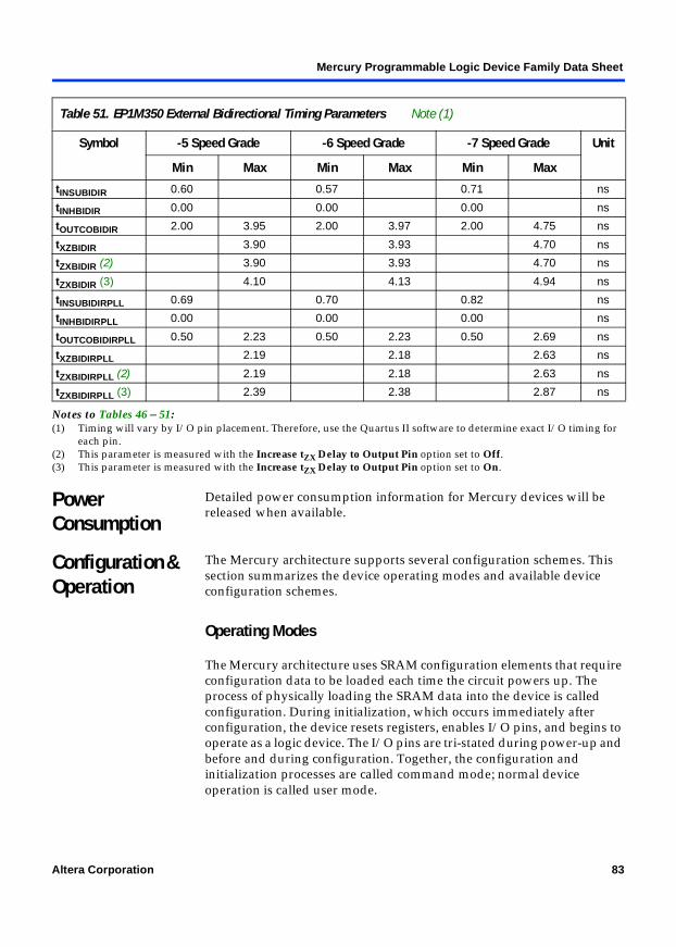
Mercury Programmable Logic Device Family Data Sheet
Developm
ent
13
Tools
Notes to Tables 46 – 51:(1) Timing will vary by I/O pin placement. Therefore, use the Quartus II software to determine exact I/O timing for
each pin.(2) This parameter is measured with the Increase tZX Delay to Output Pin option set to Off.(3) This parameter is measured with the Increase tZX Delay to Output Pin option set to On.
Power Consumption
Detailed power consumption information for Mercury devices will be released when available.
Configuration & Operation
The Mercury architecture supports several configuration schemes. This section summarizes the device operating modes and available device configuration schemes.
Operating Modes
The Mercury architecture uses SRAM configuration elements that require configuration data to be loaded each time the circuit powers up. The process of physically loading the SRAM data into the device is called configuration. During initialization, which occurs immediately after configuration, the device resets registers, enables I/O pins, and begins to operate as a logic device. The I/O pins are tri-stated during power-up and before and during configuration. Together, the configuration and initialization processes are called command mode; normal device operation is called user mode.
Table 51. EP1M350 External Bidirectional Timing Parameters Note (1)
Symbol -5 Speed Grade -6 Speed Grade -7 Speed Grade Unit
Min Max Min Max Min Max
tINSUBIDIR 0.60 0.57 0.71 ns
tINHBIDIR 0.00 0.00 0.00 ns
tOUTCOBIDIR 2.00 3.95 2.00 3.97 2.00 4.75 ns
tXZBIDIR 3.90 3.93 4.70 ns
tZXBIDIR (2) 3.90 3.93 4.70 ns
tZXBIDIR (3) 4.10 4.13 4.94 ns
tINSUBIDIRPLL 0.69 0.70 0.82 ns
tINHBIDIRPLL 0.00 0.00 0.00 ns
tOUTCOBIDIRPLL 0.50 2.23 0.50 2.23 0.50 2.69 ns
tXZBIDIRPLL 2.19 2.18 2.63 ns
tZXBIDIRPLL (2) 2.19 2.18 2.63 ns
tZXBIDIRPLL (3) 2.39 2.38 2.87 ns
Altera Corporation 83

Mercury Programmable Logic Device Family Data Sheet
Before and during device configuration, all I/O pins are pulled to VCCIO by a built-in weak pull-up resistor.
SRAM configuration elements allow Mercury devices to be reconfigured in-circuit by loading new configuration data into the device. Real-time reconfiguration is performed by forcing the device into command mode with a device pin, loading different configuration data, reinitializing the device, and resuming user-mode operation. In-field upgrades can be performed by distributing new configuration files.
Configuration Schemes
The configuration data for a Mercury device can be loaded with one of five configuration schemes (see Table 52), chosen on the basis of the target application. A configuration device, intelligent controller, or the JTAG port can be used to control the configuration of a Mercury device. When a configuration device is used, the system can configure automatically at system power-up.
By connecting the configuration enable (nCE) and configuration enable output (nCEO) pins on each device, multiple Mercury devices can be configured in any of five configuration schemes.
f For more information on configuration, see Application Note 116 (Configuring APEX 20K, FLEX 10K & FLEX 6000 Devices).
Device Pin-Outs
See the Altera web site (http://www.altera.com) or the Altera Digital Library for pin-out information.
Table 52. Data Sources for Configuration
Configuration Scheme Data Source
Configuration device Configuration device
Passive serial (PS) MasterBlasterTM or ByteBlasterMVTM download cable or serial data source
Passive parallel asynchronous (PPA) Parallel data source
Passive parallel synchronous (PPS) Parallel data source
JTAG MasterBlaster or ByteBlasterMV download cable or a microprocessor with a Jam STAPL or JBC file
84 Altera Corporation

Mercury Programmable Logic Device Family Data Sheet
Developm
ent
13
Tools
Revision History
The information contained in the Mercury Programmable Logic Device Family Data Sheet version 2.2 supersedes information published in previous versions.
Version 2.2
The following changes were made to the Mercury Programmable Logic Device Family Data Sheet version 2.2:
Updated the condition values (symbols II and IOZ) in Table 22.
Version 2.1
The following changes were made to the Mercury Programmable Logic Device Family Data Sheet version 2.1:
Updated Table 8. Updated EP1M350 regular I/O banks in Table 13. Updated Note (6) in Table 14.
Version 2.0
The following changes were made to the Mercury Programmable Logic Device Family Data Sheet version 2.0:
Changed all references to PCML to 3.3-V PCML. Updated Table 4. Updated “High-Speed Differential Interface” on page 8. Added Tables 6 through 8. Added Figures 34 and 35. Updated I/O specifications in Tables 28 and 29. Updated Mercury device capacitance in Table 43. Updated EP1M120 device timing in Tables 46 through 49. Added EP1M350 device timing in Tables 50 and 51.
Altera Corporation 85

Mercury Programmable Logic Device Family Data Sheet
Copyright © 2003 Altera Corporation. All rights reserved. Altera, The Programmable Solutions Company, thestylized Altera logo, specific device designations, and all other words and logos that are identified astrademarks and/or service marks are, unless noted otherwise, the trademarks and service marks of AlteraCorporation in the U.S. and other countries. All other product or service names are the property of theirrespective holders. Altera products are protected under numerous U.S. and foreign patents and pendingapplications, mask work rights, and copyrights. Altera warrants performance of its semiconductor productsto current specifications in accordance with Altera’s standard warranty, but reserves the right to make changesto any products and services at any time without notice. Altera assumes no responsibilityor liability arising out of the application or use of any information, product, or servicedescribed herein except as expressly agreed to in writing by Altera Corporation. Alteracustomers are advised to obtain the latest version of device specifications before relying onany published information and before placing orders for products or services.
101 Innovation DriveSan Jose, CA 95134(408) 544-7000http://www.altera.comApplications Hotline:(800) 800-EPLDCustomer Marketing:(408) 544-7104Literature Services:[email protected]
®
Altera Corporation 86