GeneralGeneral Thick Film Chip Fixed Resistor Thick Film ...

© Fraunhofer
Materials and Applications of the Ceramic Thick-Film and Multilayer Technology
Uwe Partsch, [email protected], phone: +49-351-2553-7696
www.ikts.fraunhofer.deLatest update: 25.05.2016
© Fraunhofer
Outline
Fraunhofer Gesellschaft, Fraunhofer IKTS
Department Hybrid Microsystems @ IKTS
Ceramic Thick-Film and Multilayer Technology
Application Examples
© Fraunhofer
Outline
Fraunhofer Gesellschaft, Fraunhofer IKTS
Department Hybrid Microsystems @ IKTS
Ceramic Thick-Film and Multilayer Technology
Application Examples
© Fraunhofer
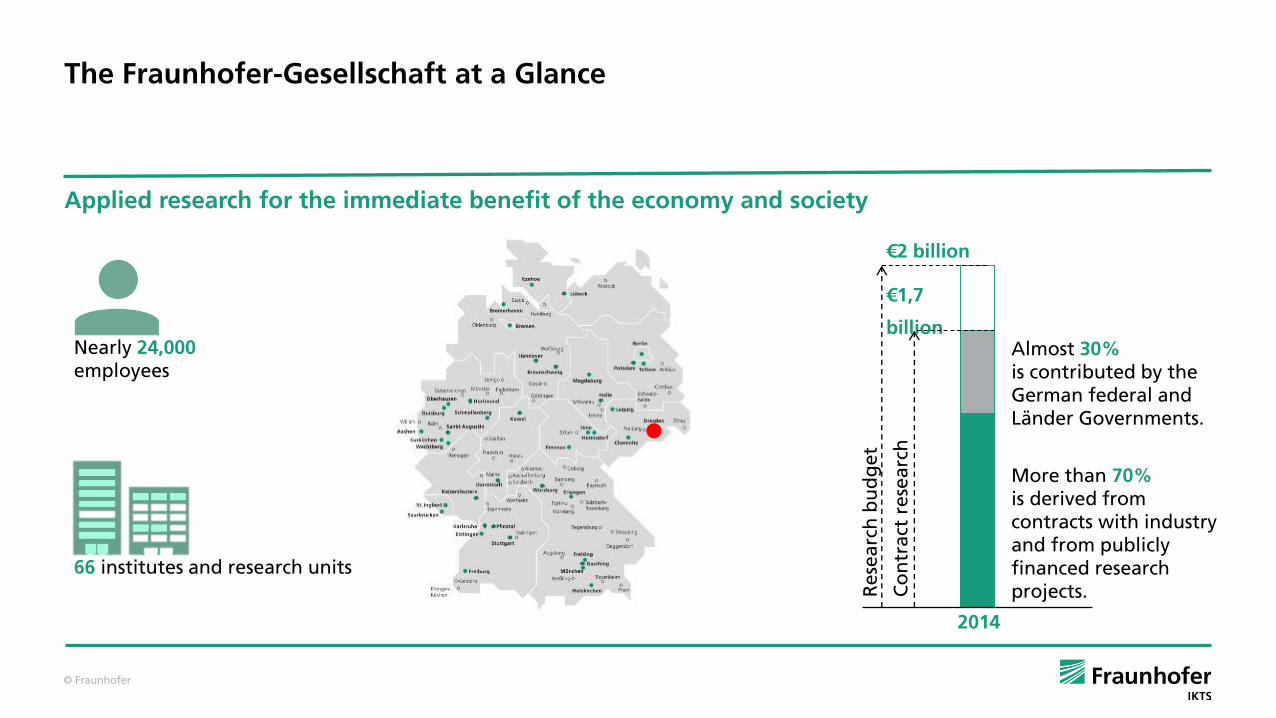
The Fraunhofer-Gesellschaft at a Glance
Applied research for the immediate benefit of the economy and society
Nearly 24,000employees
66 institutes and research units
Co
ntr
act
rese
arc
h
More than 70%is derived from contracts with industry and from publicly financed research projects.
Almost 30%is contributed by theGerman federal andLänder Governments.
Re
sea
rch
bu
dg
et
€2 billion
2014
€1,7
billion
© Fraunhofer
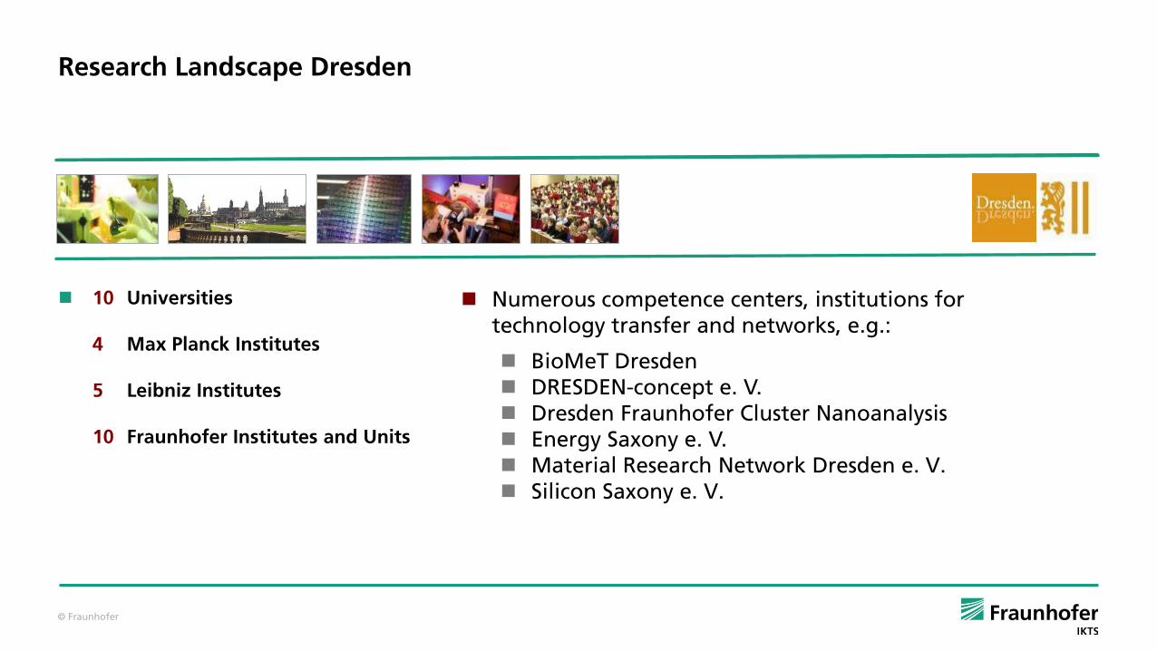
Research Landscape Dresden
10 Universities
4 Max Planck Institutes
5 Leibniz Institutes
10 Fraunhofer Institutes and Units
Numerous competence centers, institutions for technology transfer and networks, e.g.:
BioMeT Dresden DRESDEN-concept e. V. Dresden Fraunhofer Cluster Nanoanalysis Energy Saxony e. V. Material Research Network Dresden e. V. Silicon Saxony e. V.
© Fraunhofer
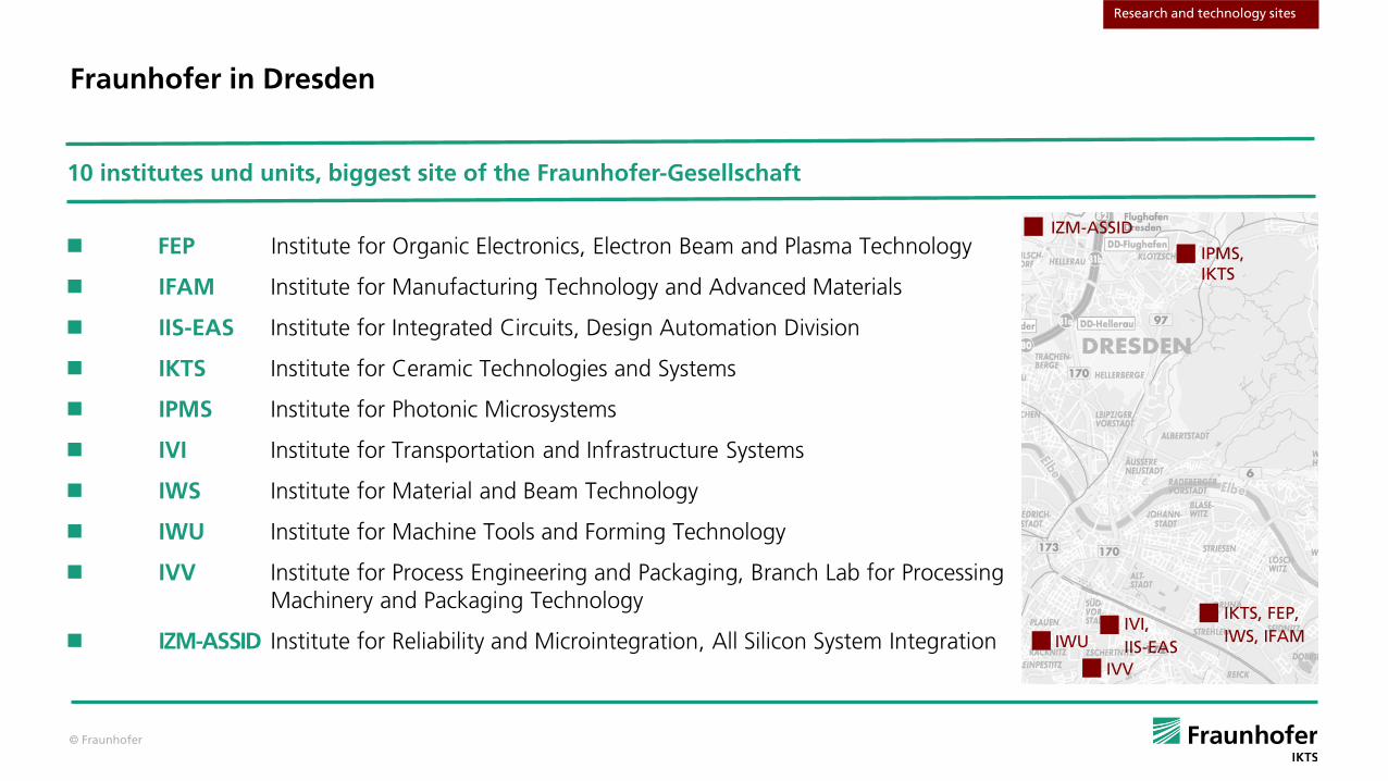
Fraunhofer in Dresden
10 institutes und units, biggest site of the Fraunhofer-Gesellschaft
FEP Institute for Organic Electronics, Electron Beam and Plasma Technology
IFAM Institute for Manufacturing Technology and Advanced Materials
IIS-EAS Institute for Integrated Circuits, Design Automation Division
IKTS Institute for Ceramic Technologies and Systems
IPMS Institute for Photonic Microsystems
IVI Institute for Transportation and Infrastructure Systems
IWS Institute for Material and Beam Technology
IWU Institute for Machine Tools and Forming Technology
IVV Institute for Process Engineering and Packaging, Branch Lab for Processing Machinery and Packaging Technology
IZM-ASSID Institute for Reliability and Microintegration, All Silicon System Integration
Research and technology sites
IPMS, IKTS
IKTS, FEP,
IWS, IFAM IVI,
IIS-EAS
IVV
IWU
IZM-ASSID
© Fraunhofer
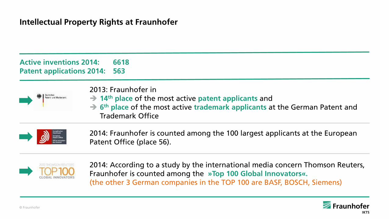
Intellectual Property Rights at Fraunhofer
Active inventions 2014: 6618Patent applications 2014: 563
2013: Fraunhofer in 14th place of the most active patent applicants and 6th place of the most active trademark applicants at the German Patent and
Trademark Office
2014: According to a study by the international media concern Thomson Reuters, Fraunhofer is counted among the »Top 100 Global Innovators«.(the other 3 German companies in the TOP 100 are BASF, BOSCH, Siemens)
2014: Fraunhofer is counted among the 100 largest applicants at the European Patent Office (place 56).
© Fraunhofer
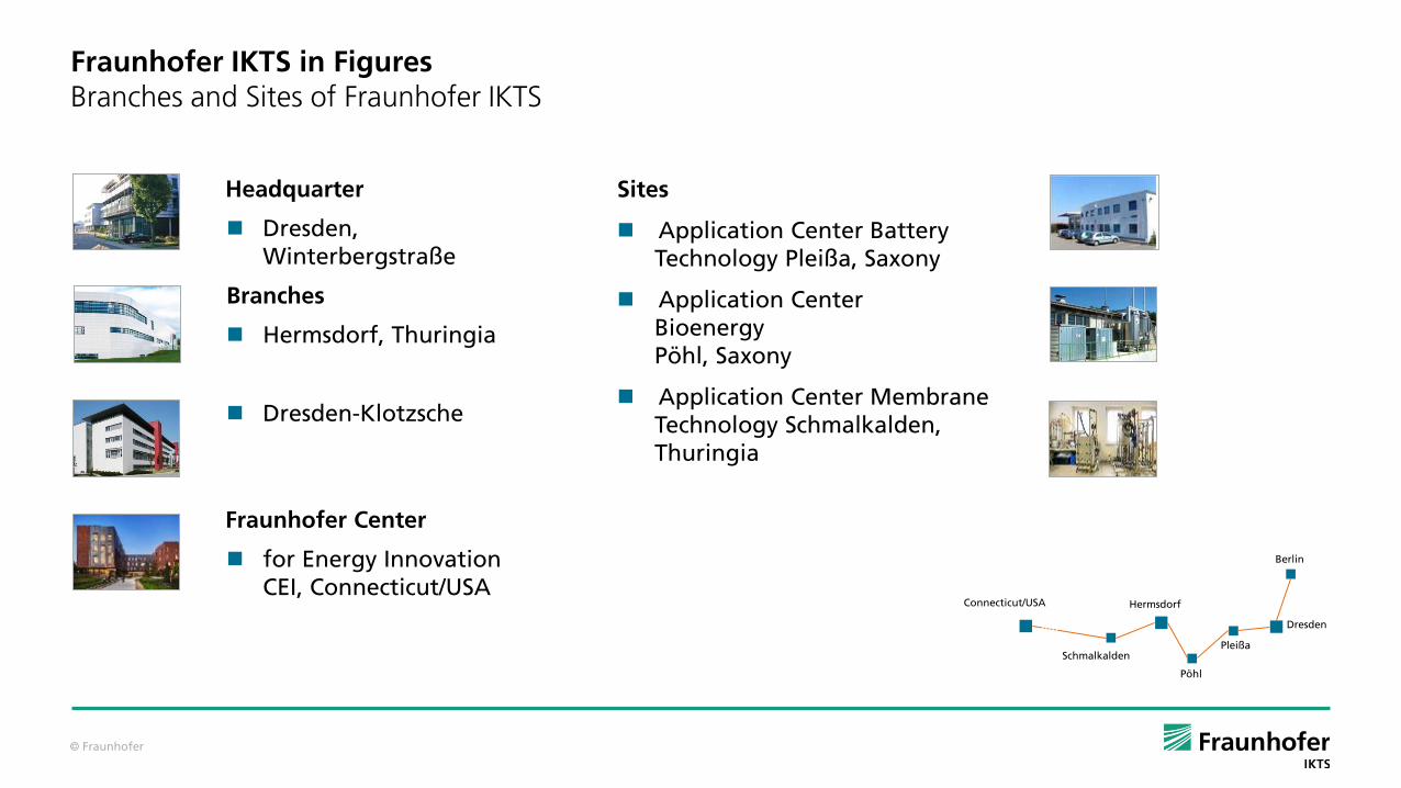
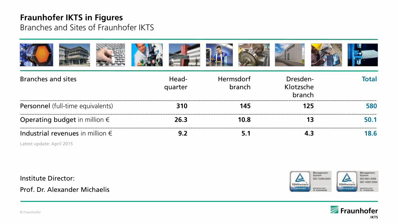
Fraunhofer IKTS in FiguresBranches and Sites of Fraunhofer IKTS
Headquarter
Dresden, Winterbergstraße
Branches
Hermsdorf, Thuringia
Dresden-Klotzsche
Fraunhofer Center
for Energy Innovation CEI, Connecticut/USA
Sites
Application Center Battery Technology Pleißa, Saxony
Application CenterBioenergy Pöhl, Saxony
Application Center Membrane Technology Schmalkalden, Thuringia
Dresden
Pleißa
Hermsdorf
Pöhl
Schmalkalden
Berlin
Connecticut/USA
IIIIII
© Fraunhofer
Fraunhofer IKTS in FiguresBranches and Sites of Fraunhofer IKTS
Branches and sites Head-quarter
Hermsdorfbranch
Dresden-Klotzsche
branch
Total
Personnel (full-time equivalents) 310 145 125 580
Operating budget in million € 26.3 10.8 13 50.1
Industrial revenues in million € 9.2 5.1 4.3 18.6
Latest update: April 2015
Institute Director:
Prof. Dr. Alexander Michaelis

© Fraunhofer
IKTS Business Divisions
MATERIALS AND PROCESSES
MECHANICAL AND AUTOMOTIVE ENGINEERING
ELECTRONICS ANDMICROSYSTEMS
ENERGYMATERIALS AND PROCESSANALYSIS
OPTICS
BIO- AND MEDICALTECHNOLOGY
ENVIRONMENTAL ANDPROCESS ENGINEERING
SYSTEMS EXPERTISE
TECHNOLOGY EXPERTISE
MATERIALSEXPERTISE
MATERIALS DIAGNOSTICS
ReliabilityQuality assurance
© Fraunhofer
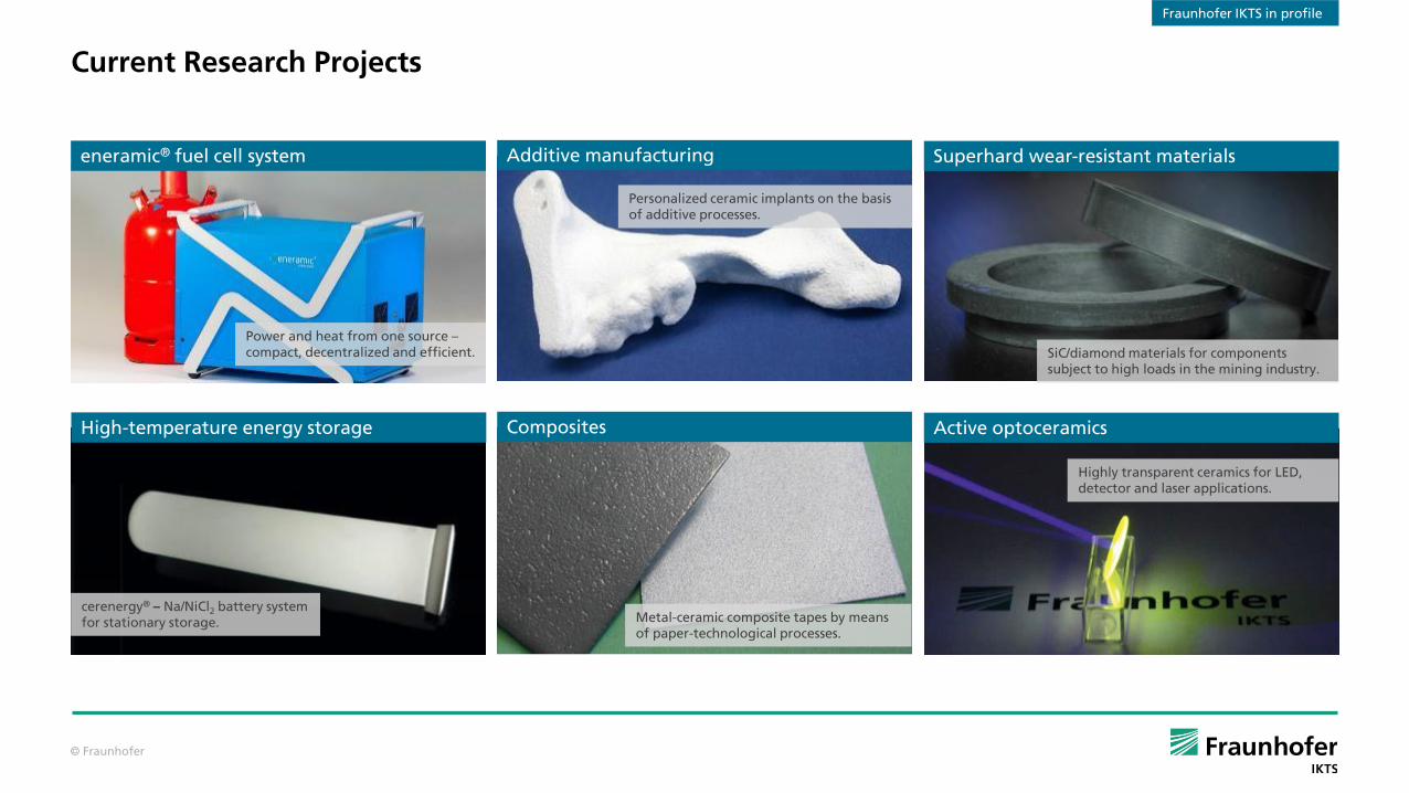
Current Research Projects
High-temperature energy storage
cerenergy® – Na/NiCl2 battery system for stationary storage.
eneramic® fuel cell system
Power and heat from one source –compact, decentralized and efficient.
Additive manufacturing
Personalized ceramic implants on the basis of additive processes.
Composites
Metal-ceramic composite tapes by means of paper-technological processes.
Active optoceramics
Highly transparent ceramics for LED, detector and laser applications.
Superhard wear-resistant materials
SiC/diamond materials for components subject to high loads in the mining industry.
Fraunhofer IKTS in profile
© Fraunhofer
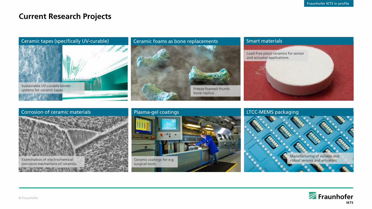
Current Research Projects
Ceramic foams as bone replacements
Freeze foamed thumb bone replica.
Ceramic tapes (specifically UV-curable)
Sustainable UV-curable binder systems for ceramic tapes.
Corrosion of ceramic materials
Examination of electrochemical corrosion mechanisms of ceramics.
Plasma-gel coatings
Ceramic coatings for e.g. surgical tools.
Smart materials
Lead-free piezo ceramics for sensor and actuator applications.
LTCC-MEMS packaging
Manufacturing of reliable and robust sensors and actuators.
Fraunhofer IKTS in profile
© Fraunhofer
Outline
Fraunhofer Gesellschaft, Fraunhofer IKTS
Department Hybrid Microsystems @ IKTS
Ceramic Thick-Film and Multilayer Technology
Application Examples

© Fraunhofer
Department Hybrid MicrosystemsFigures
3 sites, 6 working groups
48 employees
Budget 2015 approx. 5.9 Mio. €
Focused topics: Ceramic thick-film and multilayer technology
323 – Material Synthesis Powder Processing
326 – Tape Development325 – Pilot Plants Li-
Battery, PV
321 – Pastes/ Inks, Glasses 322 – C-MEMS (LTCC, HTCC) 324 – Electronic Packaging,
Reliability
Hermsdorf
Dresden
Pleißa
Hohenstein-Ernstthal
Saxony
Thuringia
© Fraunhofer
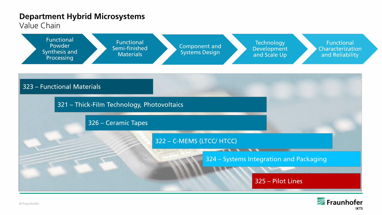
Department Hybrid MicrosystemsValue Chain
Functional Powder
Synthesis and Processing
Functional Semi-finished
Materials
Component and Systems Design
Technology Development and Scale Up
Functional Characterization and Reliability
321 – Thick-Film Technology, Photovoltaics
322 – C-MEMS (LTCC/ HTCC)
323 – Functional Materials
324 – Systems Integration and Packaging
325 – Pilot Lines
326 – Ceramic Tapes
© Fraunhofer
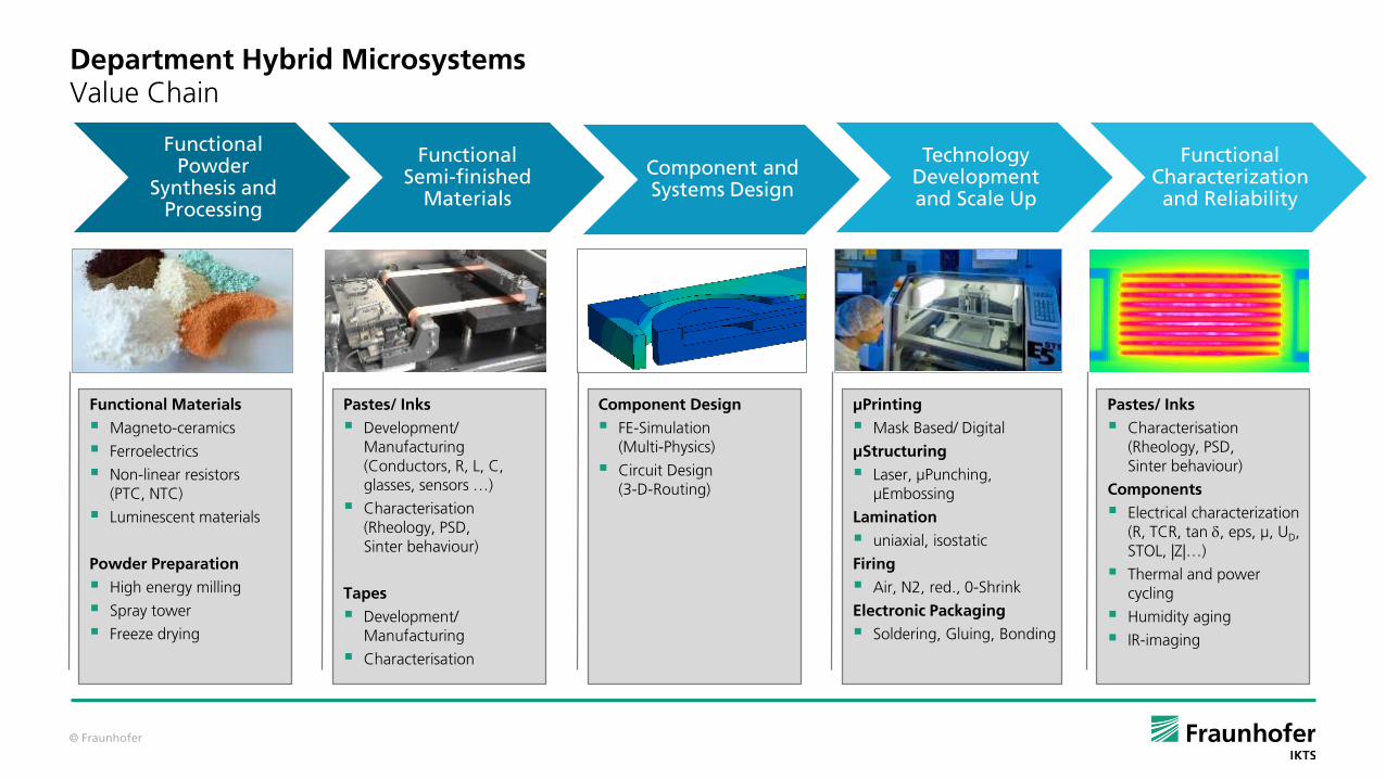
Department Hybrid MicrosystemsValue Chain
Functional Powder
Synthesis and Processing
Functional Semi-finished
Materials
Component and Systems Design
Technology Development and Scale Up
Functional Characterization and Reliability
Functional Materials
Magneto-ceramics
Ferroelectrics
Non-linear resistors (PTC, NTC)
Luminescent materials
Powder Preparation
High energy milling
Spray tower
Freeze drying
Pastes/ Inks
Development/ Manufacturing(Conductors, R, L, C, glasses, sensors …)
Characterisation(Rheology, PSD, Sinter behaviour)
Tapes
Development/ Manufacturing
Characterisation
Component Design
FE-Simulation(Multi-Physics)
Circuit Design(3-D-Routing)
µPrinting
Mask Based/ Digital
µStructuring
Laser, µPunching, µEmbossing
Lamination
uniaxial, isostatic
Firing
Air, N2, red., 0-Shrink
Electronic Packaging
Soldering, Gluing, Bonding
Pastes/ Inks
Characterisation(Rheology, PSD, Sinter behaviour)
Components
Electrical characterization (R, TCR, tan d, eps, µ, UD,STOL, |Z|…)
Thermal and power cycling
Humidity aging
IR-imaging
© Fraunhofer
Outline
Fraunhofer Gesellschaft, Fraunhofer IKTS
Department Hybrid Microsystems @ IKTS
Ceramic Thick-Film and Multilayer Technology
Application Examples
© Fraunhofer
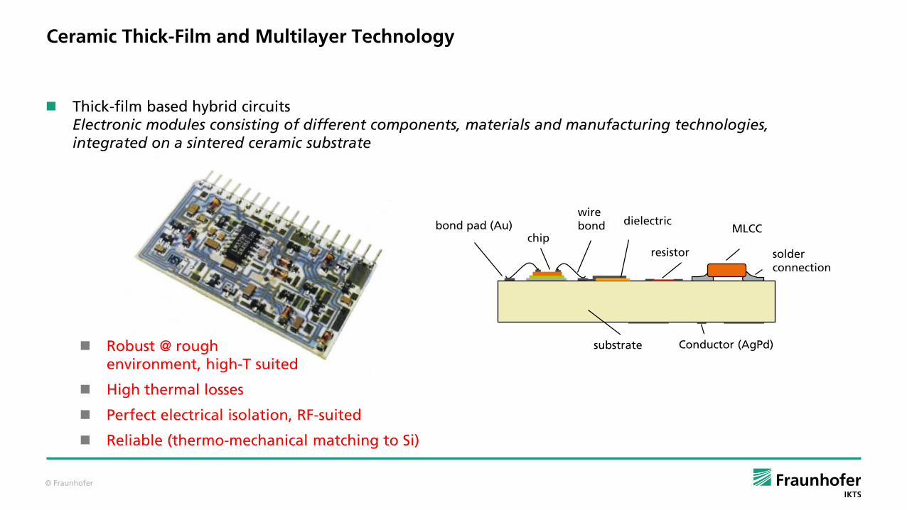
Thick-film based hybrid circuitsElectronic modules consisting of different components, materials and manufacturing technologies, integrated on a sintered ceramic substrate
Robust @ rough environment, high-T suited
High thermal losses
Perfect electrical isolation, RF-suited
Reliable (thermo-mechanical matching to Si)
bond pad (Au)chip
wire
bond dielectric
resistor
MLCC
solder
connection
substrate Conductor (AgPd)
Ceramic Thick-Film and Multilayer Technology
© Fraunhofer
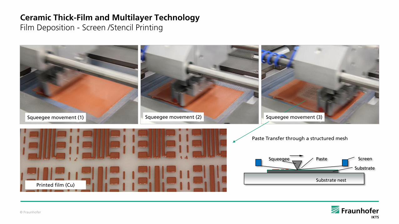
Ceramic Thick-Film and Multilayer TechnologyFilm Deposition - Screen /Stencil Printing
Paste Transfer through a structured mesh
Squeegee movement (1) Squeegee movement (2) Squeegee movement (3)
Printed film (Cu)Substrate nest
Substrate
PasteSqueegee Screen

© Fraunhofer
Functional pastes/ films
Conductor lines (Ag, AgPd, Cu, Ni, Au, Pt, W)
Passives (R, L, C)
Glasses
Sensors, actuators, ion conductors …
Structural sizes
thickness = 2.. 100 µm/ width = 0.1 .. 5 mm
process
printing, drying, firing
…
Substrate nest
Substrate
PasteSqueegee Screen
Ceramic Thick-Film and Multilayer TechnologyFilm Deposition - Screen /Stencil Printing
Screen-emulsion, -mesh © Koenen Stencil mask © Fraunhofer IKTS
10
100
1000
10000
[
Pas
]
Zeit
a.
b.
c.
Put the paste on the screen
Paste transfer through the mesh
levelling
time
time
Shear viscosity Thixotropic behavior
Shear stress by squeegee
a. b. c.
© Fraunhofer
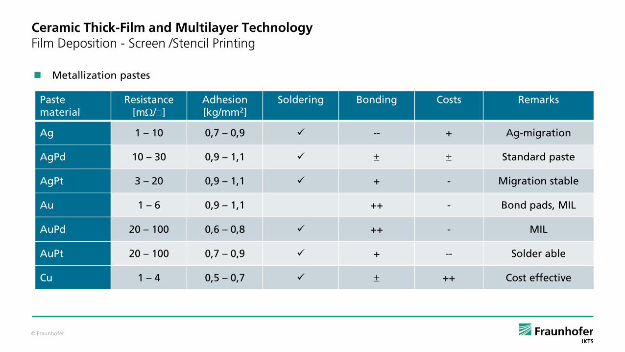
Metallization pastes
Ceramic Thick-Film and Multilayer TechnologyFilm Deposition - Screen /Stencil Printing
Paste
material
Resistance
[m/• ]
Adhesion
[kg/mm2]
Soldering Bonding Costs Remarks
Ag 1 – 10 0,7 – 0,9 -- + Ag-migration
AgPd 10 – 30 0,9 – 1,1 Standard paste
AgPt 3 – 20 0,9 – 1,1 + - Migration stable
Au 1 – 6 0,9 – 1,1 ++ - Bond pads, MIL
AuPd 20 – 100 0,6 – 0,8 ++ - MIL
AuPt 20 – 100 0,7 – 0,9 + -- Solder able
Cu 1 – 4 0,5 – 0,7 ++ Cost effective
© Fraunhofer
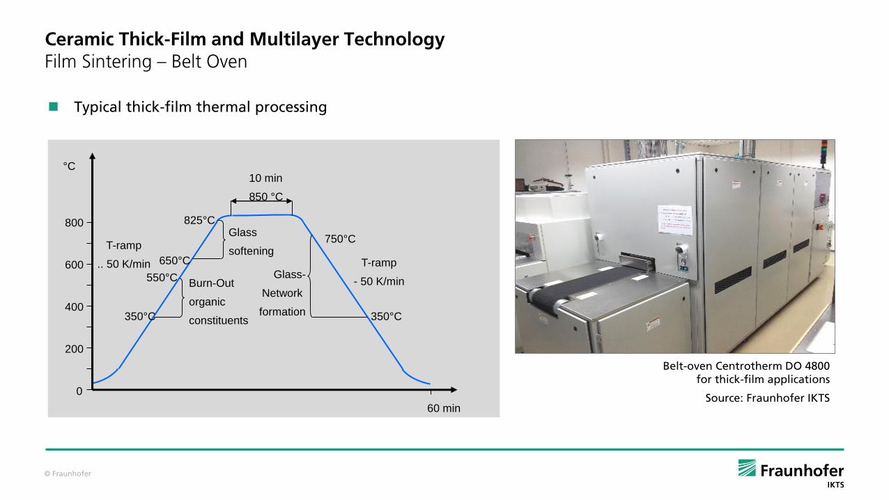
Typical thick-film thermal processing
Ceramic Thick-Film and Multilayer TechnologyFilm Sintering – Belt Oven
60 min
200
400
600
800
0
°C10 min
850 °C
Burn-Out
organic
constituents
Glass
softening
825°C
650°C
550°C
350°C
Glass-
Network
formation
750°C
350°C
T-ramp
.. 50 K/min T-ramp
- 50 K/min
Belt-oven Centrotherm DO 4800
for thick-film applications
Source: Fraunhofer IKTS
© Fraunhofer
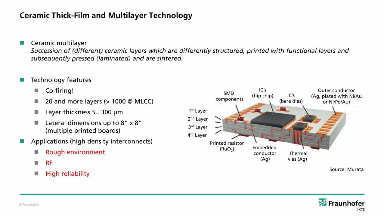
Ceramic multilayerSuccession of (different) ceramic layers which are differently structured, printed with functional layers and subsequently pressed (laminated) and are sintered.
Technology features
Co-firing!
20 and more layers (> 1000 @ MLCC)
Layer thickness 5.. 300 µm
Lateral dimensions up to 8“ x 8“ (multiple printed boards)
Applications (high density interconnects)
Rough environment
RF
High reliability
Ceramic Thick-Film and Multilayer Technology
Printed resistor
(RuO2)Embedded
conductor
(Ag)
Thermal
vias (Ag)
1st Layer
2nd Layer
3rd Layer
4th Layer
SMD
componentsIC’s
(bare dies)
IC’s
(flip chip)Outer conductor
(Ag, plated with Ni/Au
or Ni/Pd/Au)
Source: Murata

© Fraunhofer
Ceramic Thick-Film and Multilayer TechnologyProcess flow

© Fraunhofer
Ceramic Thick-Film and Multilayer TechnologyMaterials for Ceramic 3D-Substrates
Property AI2O3 HP Si3N4 AIN LTCC CCM PI FR4
Ceramics/ Glass-ceramics Steel Polymers
Sintering temperature
[°C]> 1500 > 1500 > 1400 < 900 1000 260 120
CTE [10-7/K ] 75 31 34 50 - 70 125 270 300
Thermal Conductivity
[W/mK] 20 50 150 4 - 6 25 1,2 0,2
Dielectric constant 9,5 5 10,0 3 - 5 5-6 3,5 5,0
Loss tangent (x 10-3)
@10 MHz0,3 4,5 2,0 0,1 2,0 3,0 5,0
Cost factor approx. 1 < 40 < 40 10 4 0,5 0,25
© Fraunhofer
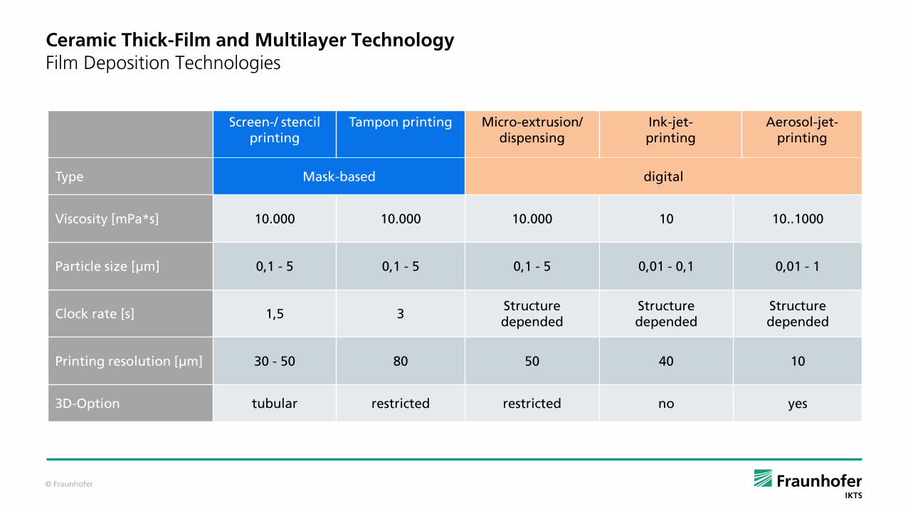
Ceramic Thick-Film and Multilayer TechnologyFilm Deposition Technologies
Screen-/ stencilprinting
Tampon printing Micro-extrusion/ dispensing
Ink-jet-printing
Aerosol-jet-printing
Type Mask-based digital
Viscosity [mPa*s] 10.000 10.000 10.000 10 10..1000
Particle size [µm] 0,1 - 5 0,1 - 5 0,1 - 5 0,01 - 0,1 0,01 - 1
Clock rate [s] 1,5 3Structure depended
Structure depended
Structure depended
Printing resolution [µm] 30 - 50 80 50 40 10
3D-Option tubular restricted restricted no yes
© Fraunhofer
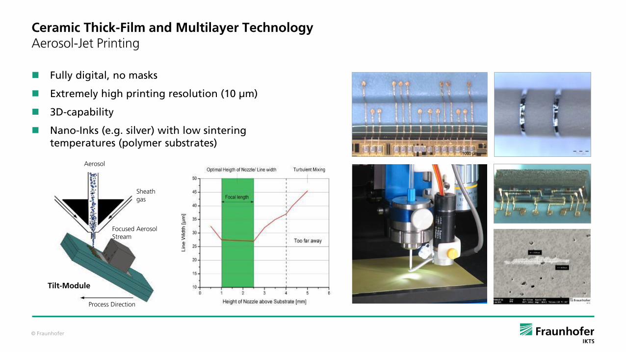
Ceramic Thick-Film and Multilayer TechnologyAerosol-Jet Printing
Fully digital, no masks
Extremely high printing resolution (10 µm)
3D-capability
Nano-Inks (e.g. silver) with low sintering temperatures (polymer substrates)
Sheath
gas
Aerosol
Process Direction
Focused Aerosol
Stream
Tilt-Module
© Fraunhofer
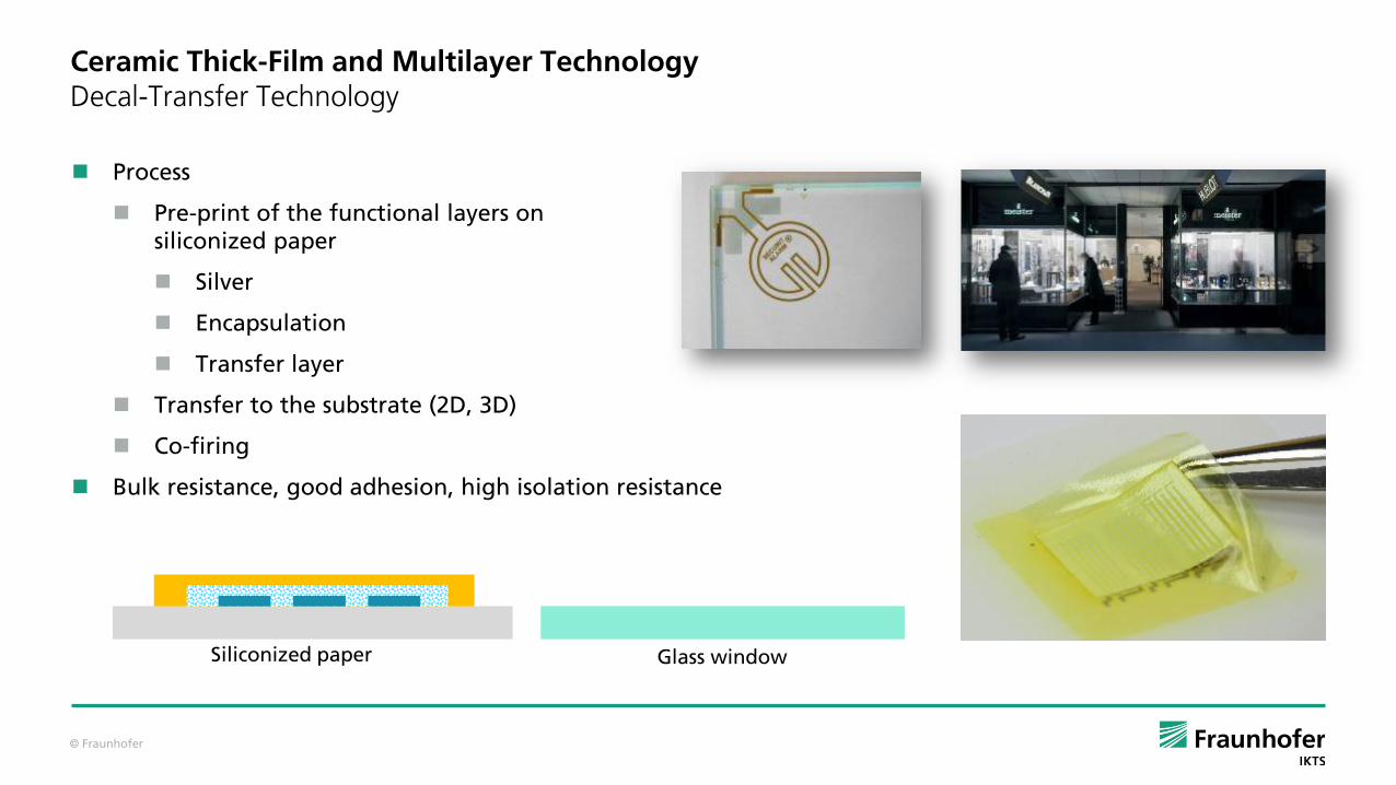
Ceramic Thick-Film and Multilayer TechnologyDecal-Transfer Technology
Process
Pre-print of the functional layers on siliconized paper
Silver
Encapsulation
Transfer layer
Transfer to the substrate (2D, 3D)
Co-firing
Bulk resistance, good adhesion, high isolation resistance
Siliconized paper Glass window
© Fraunhofer
Outline
Fraunhofer Gesellschaft, Fraunhofer IKTS
Department Hybrid Microsystems @ IKTS
Ceramic thick-film and multilayer technology
Application Examples
© Fraunhofer
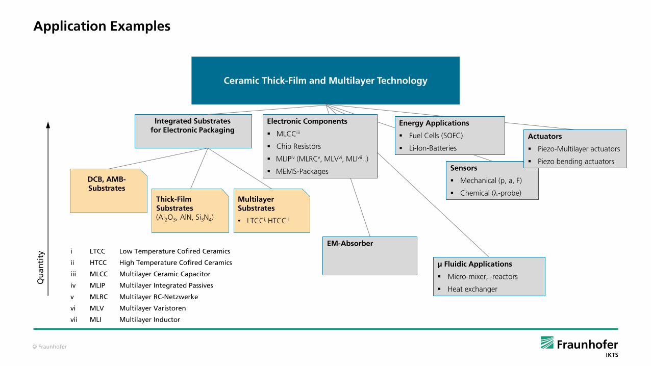
Application Examples
µ Fluidic Applications
Micro-mixer, -reactors
Heat exchanger
Ceramic Thick-Film and Multilayer Technology
Integrated Substrates for Electronic Packaging
Qu
an
tity
Sensors
Mechanical (p, a, F)
Chemical (l-probe)
Electronic Components
MLCCiii
Chip Resistors
MLIPiv (MLRCv, MLVvi, MLIvii..)
MEMS-Packages
Thick-Film Substrates (Al2O3, AlN, Si3N4)
Actuators
Piezo-Multilayer actuators
Piezo bending actuators
Multilayer Substrates
• LTCCi, HTCCii
i LTCC Low Temperature Cofired Ceramics
ii HTCC High Temperature Cofired Ceramics
iii MLCC Multilayer Ceramic Capacitor
iv MLIP Multilayer Integrated Passives
v MLRC Multilayer RC-Netzwerke
vi MLV Multilayer Varistoren
vii MLI Multilayer Inductor
DCB, AMB-Substrates
Energy Applications
Fuel Cells (SOFC)
Li-Ion-Batteries
EM-Absorber

© Fraunhofer
Application ExamplesAutomotive Applications
Ceramic Substrates/ Components
High/ low temperature
Engine 300°C
Near wheel 300°C
Exhaust 600°C
Thermal shock, cycles
Mechanical shock, vibration
Voltage spikes
Electrostatic discharge
Salt spray, humidity, break fluid, transmission fluid, engine coolant,oil
Passenger cell: 85°C
(up to 105°C)
navigation system
comfort functions
cruise control
safety systems
Components near wheel: <300°C
brake by wire
steer by wire
Around engine: <150°C (170)
propulsion system
electronic break assistant
Engine, gear control: <300°C
Source: DaimlerChrysler AG, Project: HotEl
www.mikrotechnische-produktion.de

© Fraunhofer
Application ExamplesAutomotive Applications - LTCC-based Gear Control
© Fraunhofer
Application ExamplesAutomotive Applications - LTCC-based Gear Control
© Fraunhofer
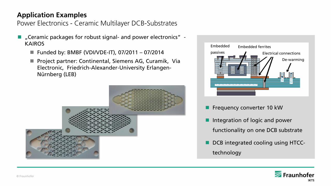
Application ExamplesPower Electronics - Ceramic Multilayer DCB-Substrates
„Ceramic packages for robust signal- and power electronics“ -KAIROS
Funded by: BMBF (VDI/VDE-IT), 07/2011 – 07/2014
Project partner: Continental, Siemens AG, Curamik, Via Electronic, Friedrich-Alexander-University Erlangen-Nürnberg (LEB)
Frequency converter 10 kW
Integration of logic and power
functionality on one DCB substrate
DCB integrated cooling using HTCC-
technology
De-warming
Electrical connections
Embedded
passives
Embedded ferrites
© Fraunhofer
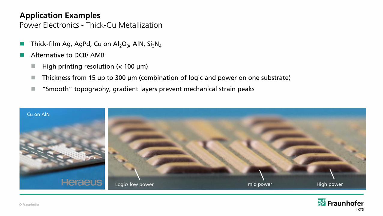
Application ExamplesPower Electronics - Thick-Cu Metallization
Thick-film Ag, AgPd, Cu on Al2O3, AlN, Si3N4
Alternative to DCB/ AMB
High printing resolution (< 100 µm)
Thickness from 15 up to 300 µm (combination of logic and power on one substrate)
“Smooth” topography, gradient layers prevent mechanical strain peaks
High powermid powerLogic/ low power
Cu on AlN
© Fraunhofer
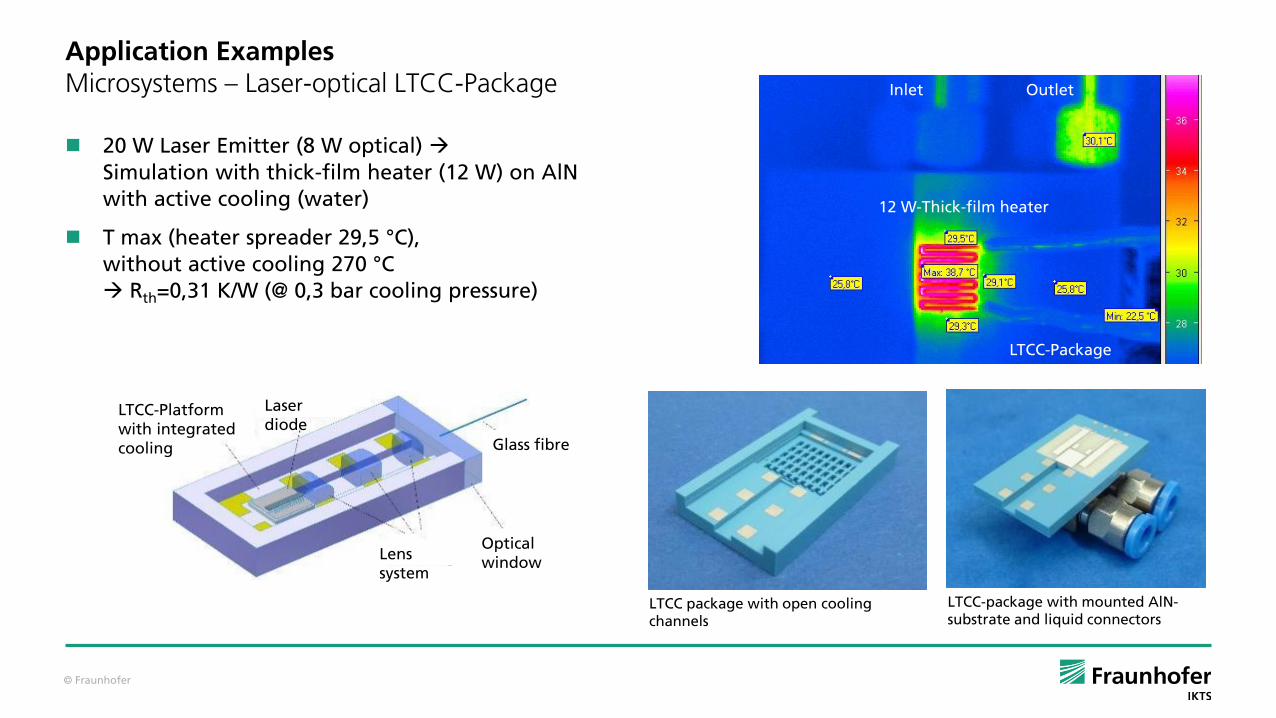
Application ExamplesMicrosystems – Laser-optical LTCC-Package
LTCC package with open cooling channels
LTCC-package with mounted AlN-substrate and liquid connectors
LTCC-Platform with integrated cooling Glass fibre
Lens system
Optical window
Laser diode
20 W Laser Emitter (8 W optical)
Simulation with thick-film heater (12 W) on AlNwith active cooling (water)
T max (heater spreader 29,5 °C),
without active cooling 270 °C Rth=0,31 K/W (@ 0,3 bar cooling pressure)
Inlet Outlet
LTCC-Package
12 W-Thick-film heater

© Fraunhofer
Deform-able mirror for beam shaping in Laser technology
6 PZT-Oktagones for the compensation of thermal effects (Correction of wave front)
Backside: PZT Thick-Film on LTCC, Frontside: Cu (plated)
© C
. R
ein
lein
, Fr
aun
ho
fer
IOF
LTCC Substrat
Cu Metallisierung
PZT Dickschicht
Au Elektrode
LTCC Membran: 220 µmDurchmesser: 34.7 mmPZT Dicke: 100 µmCu-Schicht: 150 µm
Application ExamplesMicrosystems - LTCC-based deformable Mirror

© Fraunhofer
Experimental Set-up
LTCC 45 x 45 x 0.17 mm3 with internal wiring
Piezo-electric (PZT) Actuator 25 x 4.2 x 0.1 mm3
Micro lens-Array 5.7 x 4.3 mm2
Experimental results
Deflection z = 115 µm @ E = 2 kV/mm, linear behavior
Blocking force FB = 110 mN @ E = 2 kV/mm
Mikrolinsen-Array
PZT-DiS-Aktuator
LTCC-Rahmen
deflection
PZT thick film
Actuator design
Application ExamplesMicrosystems - LTCC-based Micro-Positioning Stage
© Fraunhofer
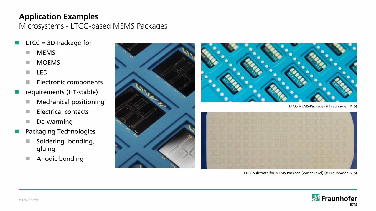
Application ExamplesMicrosystems - LTCC-based MEMS Packages
LTCC = 3D-Package for
MEMS
MOEMS
LED
Electronic components
requirements (HT-stable)
Mechanical positioning
Electrical contacts
De-warming
Packaging Technologies
Soldering, bonding, gluing
Anodic bonding
LTCC-MEMS-Package (© Fraunhofer IKTS)
LTCC-Substrate for MEMS-Package (Wafer Level) (© Fraunhofer IKTS)
© Fraunhofer
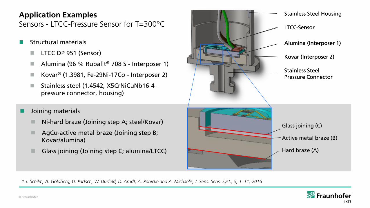
Application ExamplesSensors - LTCC-Pressure Sensor for T=300°C
Structural materials
LTCC DP 951 (Sensor)
Alumina (96 % Rubalit® 708 S - Interposer 1)
Kovar® (1.3981, Fe-29Ni-17Co - Interposer 2)
Stainless steel (1.4542, X5CrNiCuNb16-4 –pressure connector, housing)
* J. Schilm, A. Goldberg, U. Partsch, W. Dürfeld, D. Arndt, A. Pönicke and A. Michaelis, J. Sens. Sens. Syst., 5, 1–11, 2016
LTCC-Sensor
Alumina (Interposer 1)
Kovar (Interposer 2)
Stainless Steel Pressure Connector
Stainless Steel Housing
LTCC-Sensor
Alumina (Interposer 1)
Kovar (Interposer 2)
Stainless Steel Pressure Connector
Glass joining (C)
Active metal braze (B)
Hard braze (A)
Joining materials
Ni-hard braze (Joining step A; steel/Kovar)
AgCu-active metal braze (Joining step B; Kovar/alumina)
Glass joining (Joining step C; alumina/LTCC)
© Fraunhofer
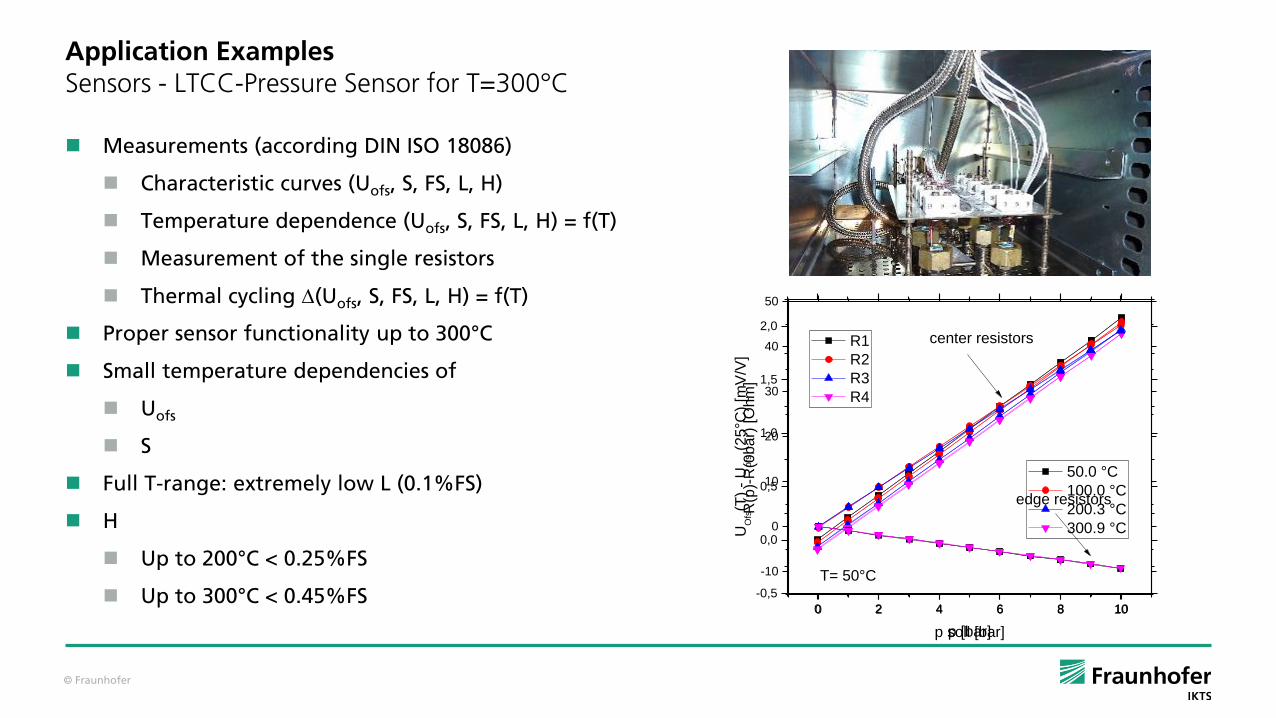
Application ExamplesSensors - LTCC-Pressure Sensor for T=300°C
Measurements (according DIN ISO 18086)
Characteristic curves (Uofs, S, FS, L, H)
Temperature dependence (Uofs, S, FS, L, H) = f(T)
Measurement of the single resistors
Thermal cycling (Uofs, S, FS, L, H) = f(T)
Proper sensor functionality up to 300°C
Small temperature dependencies of
Uofs
S
Full T-range: extremely low L (0.1%FS)
H
Up to 200°C < 0.25%FS
Up to 300°C < 0.45%FS0 2 4 6 8 10
-0,5
0,0
0,5
1,0
1,5
2,0
UO
fs(T
) -
Uofs (
25
°C)
[mV
/V]
p [bar]
50.0 °C
100.0 °C
200.3 °C
300.9 °C
0 2 4 6 8 10
-10
0
10
20
30
40
50
R(p
)-R
(0b
ar)
[O
hm
]
p soll [bar]
R1
R2
R3
R4
center resistors
edge resistors
T= 50°C
© Fraunhofer
Thank you for your attention!
Further information:


![Thermal Conductivity of Thick Film Tungsten Metallization ... · the metallization/ceramic interface adhesion mechanism which has been explained by the glass penetration theory [3].](https://static.fdocuments.net/doc/165x107/5e9504fbc2e4a97df63c0bd5/thermal-conductivity-of-thick-film-tungsten-metallization-the-metallizationceramic.jpg)
