Metallic and Ceramic Thin Film Thermocouples
106
University of Rhode Island University of Rhode Island DigitalCommons@URI DigitalCommons@URI Open Access Master's Theses 2013 Metallic and Ceramic Thin Film Thermocouples Metallic and Ceramic Thin Film Thermocouples Ian M. Tougas University of Rhode Island, [email protected] Follow this and additional works at: https://digitalcommons.uri.edu/theses Recommended Citation Recommended Citation Tougas, Ian M., "Metallic and Ceramic Thin Film Thermocouples" (2013). Open Access Master's Theses. Paper 7. https://digitalcommons.uri.edu/theses/7 This Thesis is brought to you for free and open access by DigitalCommons@URI. It has been accepted for inclusion in Open Access Master's Theses by an authorized administrator of DigitalCommons@URI. For more information, please contact [email protected].
Transcript of Metallic and Ceramic Thin Film Thermocouples
University of Rhode Island University of Rhode Island
DigitalCommons@URI DigitalCommons@URI
Open Access Master's Theses
2013
Metallic and Ceramic Thin Film Thermocouples Metallic and Ceramic Thin Film Thermocouples
Ian M. Tougas University of Rhode Island, [email protected]
Follow this and additional works at: https://digitalcommons.uri.edu/theses
Recommended Citation Recommended Citation Tougas, Ian M., "Metallic and Ceramic Thin Film Thermocouples" (2013). Open Access Master's Theses. Paper 7. https://digitalcommons.uri.edu/theses/7
This Thesis is brought to you for free and open access by DigitalCommons@URI. It has been accepted for inclusion in Open Access Master's Theses by an authorized administrator of DigitalCommons@URI. For more information, please contact [email protected].
METALLIC AND CERAMIC THIN FILM THERMOCOUPLES
BY
IAN M. TOUGAS
A THESIS SUBMITTED IN PARTIAL FULFILLMENT OF THE
REQUIREMENTS FOR THE DEGREE OF
MASTER OF SCIENCE
IN
CHEMICAL ENGINEERING
UNIVERSITY OF RHODE ISLAND
2013
MASTER OF SCIENCE IN CHEMICAL ENGINEERING THESIS
OF
IAN M. TOUGAS
APPROVED:
Thesis Committee:
Major Professor Otto Gregory
Hamouda Ghonem
Everett Crisman
David Heskett
Nasser H. Zawia
DEAN OF THE GRADUATE SCHOOL
UNIVERSITY OF RHODE ISLAND
2013
ABSTRACT
Operating temperatures in the hot sections of modern gas turbine engines reach as
high as 1500°C, making in situ monitoring of the severe temperature gradients on the
surface of components rather difficult. Therefore, there is a need to develop
thermocouples which can stably measure temperature in these harsh environments.
Refractory metal and ceramic thin film thermocouples are well suited for this task
since they have chemical and electrical stability at high temperatures in oxidizing
atmospheres, they are compatible with thermal barrier coatings employed on engine
components, have higher sensitivity than conventional wire thermocouples, and they
are non-invasive to the engine environment. In this masters thesis, thin film
combinatorial chemistry for materials discovery and characterization was the primary
tool used to optimize thermo-element materials for thin film thermocouples. The
resulting sensors based on ceramics, such as indium oxide and indium tin oxide, as
well as others based on refractory metals, such as platinum and palladium, exhibited
remarkable stability for many cycles at temperatures above 1000°C.
iii
ACKNOWLEDGMENTS
I would like to formally distinguish Dr. Otto J. Gregory for the outstanding
guidance and expertise, as an advisor and professor; he has given me at the University
of Rhode Island during the four years of my undergraduate and graduate research
assistantship. He has inspired me to achieve demanding goals beyond my expectations
through various research projects, the completion of many courses in engineering and
materials science, and through publishing manuscripts in well known scientific
journals. Furthermore, I would like to thank the members of my thesis committee, Dr.
Everett E. Crisman, Dr. Hamouda Ghonem, and Dr. David Heskett for their help in the
completion of my masters thesis program in chemical engineering.
I could not have completed the work contained in this thesis without the help of
my fellow researchers at the URI Center for Sensors and Instrumentation Research:
Michael Platek, Mitchell Beck, Yun Chu, Ximing Chen, Emily Moorehead, Robert
Balikov, and Matin Amani. Additionally, I would like to thank our partners who
provided the research grants I worked under over the past four years: Mesoscribe
Technologies, Inc. of Saint James, NY, NASA Glenn Research Center of Cleveland,
Ohio, and Rolls-Royce Indianapolis. Finally, I would like to thank Sheryl Girard and
Brenda Moyer of the URI department of chemical engineering for their support and
help in my academic and research efforts.
iv
PREFACE
The work presented in this thesis is the continuation of the high temperature
sensors research pioneered by Dr. Gregory and his research group for the past thirty
years at URI. This thesis is presented in manuscript format with an introductory
chapter one, three manuscripts as chapters two through four, and a fifth chapter
highlighting ideas for the future continuation of this work. Chapters two present a
manuscript on the stability of indium tin oxide based thermocouples. Chapter three
contains a manuscript on the use of thin film combinatorial chemistry techniques for
optimizing the thermoelectric properties of Cu-In-O based thermocouples. The fourth
chapter presents an investigation of platinum-palladium thin film thermocouples.
Lastly, chapter five elaborates on the future work which can be performed to further
develop the work presented in this thesis.
Chapter one gives an introduction to thin film instrumentation of gas turbine
engines, an overview of thin film combinatorial chemistry and how it was developed
for the work in this thesis, and an elaboration on how the thermocouples in the three
manuscripts were tested.
Chapter two presents the first manuscript, “Stability and Microstructure of Indium
Tin Oxynitride Thin Film Thermocouples” by Otto J. Gregory, Matin Amani, Ian M.
Tougas, and Alvin J. Drehman which discusses improvements to the thermoelectric
stability of thin film thermocouples based on indium oxide and indium tin oxide and
the resulting microstructures of the films. More specifically, reactive sputtering of
indium oxide and indium tin oxide in nitrogen was used to metastably retain nitrogen
in the films to form indium oxynitride or indium tin oxynitride. The slower sintering
v
kinetics of nitrides relative to oxides was utilized to inhibit microstructural changes
during thermal cycling, which often leads to sensor instability. This manuscript is
currently published in the Journal of the American Ceramic Society (Volume 95, Issue
2, pages 705-710 February 2012).
Chapter three contains the second manuscript, “Thermoelectric Properties and
Microstructure of Cu-In-O Thin Films” by Otto J. Gregory, Ian M. Tougas, Matin
Amani, and Everett E. Crisman. It presents the thermoelectric properties of hundreds
of thin films in the CuO-In2O3 system using combinatorial sputtering techniques.
Optimized p-type and n-type semiconducting materials were rapidly identified, a
characteristic that is difficult to achieve using any technique in a single binary oxide
system. Furthermore, it demonstrates the merits of using thin film combinatorial
chemistry to identify ideal thermoelectric materials, such as a p-type and n-type
material, to produce stable, high output thermocouple junctions. This manuscript is
currently being reviewed by the Journal of Electronic Materials for publication.
Chapter four presents the third manuscript, “Thin film platinum-palladium
thermocouples for gas turbine engine applications” by Ian M. Tougas and Otto J.
Gregory where the thermoelectric properties and microstructures of platinum-
palladium thin film thermocouples are presented. These sputtered thermocouples were
found to be more stable than any other metal thin film thermocouple to date, including
the type-S thin film thermocouple (platinum-platinum/10% rhodium) that is currently
the aerospace industry standard. Furthermore, the stability of these thin film
thermocouples was on the same order as conventional wire thermocouples (type-K)
operating in the same temperature range (above 1000°C). This manuscript is currently
vi
being reviewed by Thin Solid Films for publication. Additionally, a provisional filing
for a United States patent based on this technology has been filed.
Chapter five discusses future ideas for the continuation of the work presented in
this thesis. Research using both ceramic and metal thin film thermocouples in terms of
modern gas turbine engine requirements is elaborated on as well as the current state of
the ongoing work involving thermoelectric Cu-In-O thin films.
A provisional United States patent based on the implementation of thin film
sensors, such as those studied in this thesis, on the surface of SiC-SiC ceramic matrix
composites (CMC) has been filed.
vii
TABLE OF CONTENTS
ABSTRACT .................................................................................................................. ii
ACKNOWLEDGMENTS ........................................................................................ iiiii
PREFACE .................................................................................................................. ivv
TABLE OF CONTENTS ......................................................................................... viiii
LIST OF TABLES ....................................................................................................... x
LIST OF FIGURES .................................................................................................... xi
CHAPTER 1 ................................................................................................................. 1
INTRODUCTION ................................................................................................... 1
1.1 Thin Film Instrumentation of Gas Turbine Engines……………….1
1.2 Thin Film Combinatorial Chemistry……………………………….3
1.3 Thermocouple Testing……………………………………………12
CHAPTER 2 ............................................................................................................. ..16
STABILITY AND MICROSTRUCTURE OF INDIUM TIN OXYNITRIDE
THIN FILMS…………………………………………………………………16
2.1 Abstract…………………………………………………………...16
2.2 Introduction……………………………………………………….17
2.3 Experimental Procedure…………………………………………..20
2.4 Results and Discussion……………………………………………22
2.5 Conclusion………………………………………………………..36
List of References…………………………………………………….38
CHAPTER 3 ............................................................................................................... 41

viii
THERMOELECTRIC PROPERTIES AND MICROSTRUCTURE OF Cu-In-
O THIN FILMS………………………………………………………………41
3.1 Abstract…………………………………………………………...41
3.2 Introduction……………………………………………………….42
3.3 Experimental Procedure…………………………………………..43
3.4 Results and Discussion……………………………………………45
3.4.1 Thermoelectric Properties………………………………45
3.4.2 Crystallography and Phases Present……………………48
3.4.3 Microstructure…………………………………………..49
3.5 Conclusion………………………………………………………..53
List of References…………………………………………………….54
CHAPTER 4 ............................................................................................................... 56
THIN FILM PLATINUM-PALLADIUM THERMOCOUPLES FOR GAS
TURBINE ENGINE APPLICATIONS………………………………………56
4.1 Abstract…………………………………………………………...56
4.2 Introduction……………………………………………………….57
4.3 Experimental details………………………………………………59
4.4 Results and Discussion……………………………………………62
4.4.1 Thermoelectric measurements………………………….62
4.4.2 AES depth profiling and SEM imaging………………...71
4.5 Conclusion………………………………………………………..77
List of References…………………………………………………….79
CHAPTER 5 ............................................................................................................... 81

ix
FUTURE WORK……………………………………………………………..81
5.1 Thin Film Thermocouples………………………………………...81
List of References…………………………………………………….84
BIBLIOGRAPHY ...................................................................................................... 85

x
LIST OF TABLES
TABLE PAGE
Table 1. Sputtering conditions of platinum, indium oxide and ITO films……………21
Table 2. Activation energies associated with the electrical conductivities of various
oxide and oxynitride films as a function of thermal cycling………………………….32
Table 3. Thermoelectric response and drift rate of In2O3 vs. ITO and InON vs. ITON
thin film thermocouples………………………………………………………………35
Table 4. Sputtering parameters used for the deposition of platinum and palladium….61
Table 5. Drift rates of platinum:palladium thermocouples on alumina and mullite at
various temperatures………………………………………………………………….68
Table 6. Equation parameters for the relationship of temperature difference to voltage
for platinum:palladium thermocouples on alumina and mullite surfaces.…….……...69
xi
LIST OF FIGURES
FIGURE PAGE
Figure 1. Thermocouple measurement circuit showing the junction of two dissimilar
materials subject to a temperature difference along its length. The resulting
thermoelectric voltage is measured as a function of the applied temperature
difference………………………………………………………………………………4
Figure 2. General Electric J85 engine test setup instrumented with thin film
thermocouples. Lead wires were embedded in the root of the parts containing
thermocouples to retrieve voltage signals during thermal cycling. (Image provided by
MesoScribe Technologies, Inc.)…………………………….………………………….5
Figure 3. Two thin film thermocouples fabricated by radio frequency sputtering onto a
ceramic substrate. Length of beam is 7 inches...……………………………………….6
Figure 4. Combinatorial library fabricated by simultaneous sputtering from CuO and
In2O3 targets. A composition gradient (note the color change of the thermoelements
from left to right) was formed between the two targets resulting in the fabrication of
several hundred thermocouples with unique compositions in a single sputtering run....9
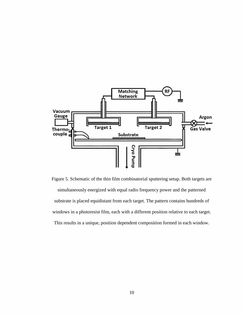
Figure 5. Schematic of the thin film combinatorial sputtering setup. Both targets are
simultaneously energized with equal radio frequency power and the patterned
xii
substrate is placed equidistant from each target. The pattern contains hundreds of
windows in a photoresist film, each with a different position relative to each target.
This results in a unique, position dependent composition formed in each window.…10
Figure 6. Flow chart of the thin film combinatorial chemistry procedure developed for
the work in this thesis…………………………………………………………………11
Figure 7. Custom tube furnace testing rig for thin film thermocouples deposited on
ceramic beams, which applied a horizontal temperature difference along the length of
the thermocouple measured with type-K and type-S wire thermocouples. This setup
simulated the severe temperature gradients on the surface of components inside gas
turbine engine hot sections……………………………………………………………13
Figure 8. Combinatorial library thermocouples being tested for thermoelectric
properties. A hot probe was positioned at the hot junction of each thermocouple to
apply a temperature difference along its length and the thermoelectric voltage was
recorded. Hot probe not shown in image……………………………………………..15
Figure 9. SEM micrographs of (a) InON film (b) fracture surface, (c) In2O3 film and
(d) fracture surface on compact alumina after annealing in air at 1250°C for ten hours.
Note the dense layer formed on the surface of the InON film and the porosity
contained beneath (b). The In2O3 film (d) had less porosity than the InON film…….24
xiii
Figure 10. SEM micrograph of InON film prepared on c-axis sapphire after annealing
in air at 1250°C for ten hours. Note the faceted particles and porosity. Less porosity is
seen here relative to the fracture surface of the same film (Figure 9b)……………….25
Figure 11. X-ray diffraction patterns of In2O3 and InON films after annealing in air at
1250°C for ten hours. Peaks corresponding to In2O3 and InN were present in the InON
film indicating that metastable nitrogen was retained in the film as part of a indium
nitride phase…………………………………………………………………………..26
Figure 12. Isothermal constrained shrinkage ((V0-V)/V0) of In2O3 films prepared in Ar
(blue square), Ar/O2 (green circle) and Ar/N2 (red triangle) plasmas at 1300°C as a
function of time……………………………………………………………………….28
Figure 13. Electrical resistivity of In2O3 and ITO films prepared in Ar and Ar/N2
plasmas…......................................................................................................................30
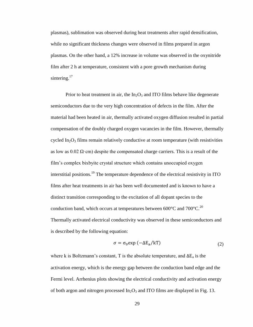
Figure 14. Seebeck coefficient of In2O3 films prepared in Ar, Ar/N2, and Ar/O2
plasmas………………………………………………………………………………..33
Figure 15. Thermoelectric output and hysteresis (heating: red, cooling: blue) of
ceramic thin film thermocouples……………………………………………………...37
xiv
Figure 16. Map of the thermoelectric voltage as a function of composition (at%
indium) for nitrogen annealed combinatorial library (a temperature difference of T =
7.7 °C was applied across individual thermocouples)...….…………………………..46
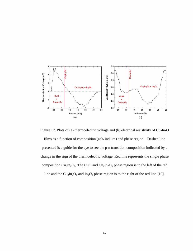
Figure 17. Plots of (a) thermoelectric voltage and (b) electrical resistivity of Cu-In-O
films as a function of composition (at% indium) and phase region. Dashed line
presented is a guide for the eye to see the p-n transition composition indicated by a
change in the sign of the thermoelectric voltage. Red line represents the single phase
composition Cu2In2O5. The CuO and Cu2In2O5 phase region is to the left of the red
line and the Cu2In2O5 and In2O3 phase region is to the right of the red line [10]….....47
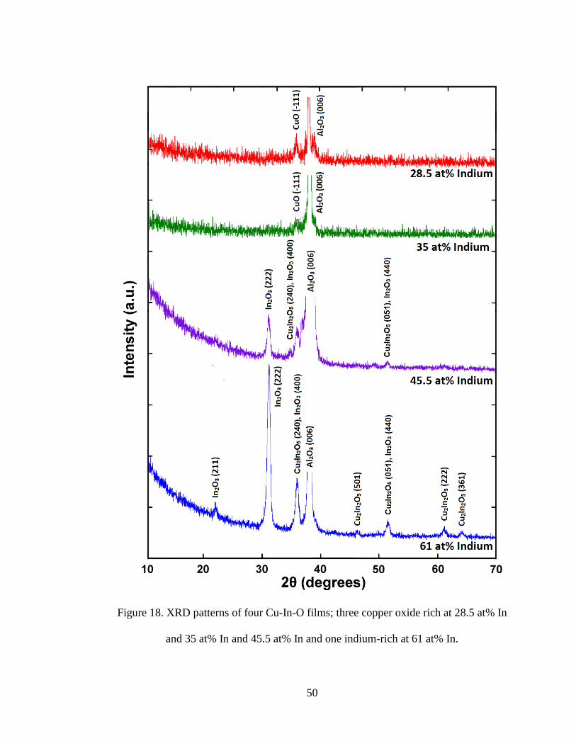
Figure 18. XRD patterns of four Cu-In-O films; three copper oxide rich at 28.5 at% In
and 35 at% In and 45.5 at% In and one indium-rich at 61 at% In……………………50
Figure 19. TEM micrographs and electron diffraction patterns for: (a, b) typical as
deposited films showing totally amorphous and uniform structure, (c, d) at onset of
crystallinity (after 400 °C, 5 h nitrogen anneal), and (e, f) after phase separation of the
film into large copper-rich particles…………………………………………………..51
Figure 20. TEM micrographs and electron diffraction patterns showing phase
separation in a Cu-In-O film (50 at% In): (a) low magnification image indicating
copper-rich precipitates in an amorphous background, (b) high resolution image of
copper-rich region with (c) corresponding electron diffraction pattern and (d) high
xv
resolution image of (nearly) amorphous background with (e) corresponding electron
diffraction pattern……………………………………………………………………..52
Figure 21. Thermoelectric output of two different platinum:palladium thermocouples
on alumina (a) and mullite (b). A peak hot junction temperature of 900 °C was used in
each case……………………………………………………………………………...63
Figure 22. Hysteresis upon heating/cooling platinum:palladium thermocouples on
alumina and mullite. Corresponds to second cycle of thermoelectric data in Figure 1a
and Fig. 1b…………………………………………………………………………….65
Figure 23. Seebeck coefficient of platinum:palladium thermocouples on alumina and
mullite as a function of temperature and substrate……………………...…………….67
Figure 24. Drift rates of platinum:palladium thermocouples as a function of
temperature. Note the Arrhenius temperature dependance of the drift rates…………70
Figure 25. SEM micrographs using backscatter electron imaging (BSEI) of various
thin film thermocouple legs after high temperature cycling: platinum on alumina (a);
palladium on alumina (b); platinum on mullite (c); and palladium on mullite (d). Each
film exhibited dewetting with distinctly different microstructures due to long term
high temperature exposure……………………………………………………………74
xvi
Figure 26. SEM micrographs (BSEI) of the faceted striations in the thermocouple legs
after high temperature cycling: palladium on alumina (a); platinum on mullite (b)….76
1
CHAPTER 1
INTRODUCTION
1.1 Thin Film Instrumentation of Gas Turbine Engines
The next generation of gas turbine engine technology, used for propulsion and
energy generation systems, is utilizing increasingly advanced materials which are
designed to handle the harsh environments inside these engines. With advances in
engine materials comes the need for developing new instrumentation which can handle
the harsher environment and monitor the operating conditions inside the engine during
testing. Designers must gain an understanding of the operating conditions and perform
diagnostics in order to ensure an engine is safe for use in an aircraft or other
application. More specifically, technological advancement in gas turbine engine
technology brings several improvements such as lighter engine components with
superior thermomechanical properties, more advanced thermal barrier coatings (TBC)
for components such as the turbine blades, and higher operating temperatures to
improve overall combustion efficiency and reduce harmful emissions. Therefore,
design and implementation of sensors which will be used to monitor operating
conditions and perform diagnostics in these modern engines is becoming an
increasingly difficult task.
Many issues arise when attempting to integrate sensors inside modern gas
turbines, especially since they operate with severe conditions such as supersonic
nozzle velocities, rotational forces exceeding fifty thousand g, and temperatures which
2
reach as high as 1500°C in the hot section. Conventional wire sensors cannot reliably
withstand these conditions due to their geometrical interference with combustion gas
flow patterns and vibrational modes of rotating parts. Furthermore, they also require
high temperature adhesives to integrate them into engine components. As an
alternative, research efforts have focused on thin film sensors to replace conventional
wire sensors. Thin films not only avoid many of the issues invoked by wire sensors
but also introduce other advantages. They do not interfere with gas flow patterns
because their thicknesses, on the order of micrometers, lie below the boundary layer
thickness formed on instrumented engine component surfaces, which is below 1 mm,
and with masses on the order of micrograms, they do not affect the vibrational modes
of rotating parts. In addition, their properties are not affected by the rotational forces
inside the engine and they also have much faster signal response times due to low
thermal mass relative to wire sensors. Thin films can be directly deposited onto the
surface of components without surface preparation and the need for high temperature
adhesives. In this way, more accurate surface measurements can be made.
Temperature measurements on the surface of gas turbine engine components
during operation is an integral part of the testing effort which goes into each gas
turbine engine prior to implementation on an aircraft or in a power generation
application. Thin film thermocouples have been developed to provide stable
temperature measurements during engine testing and diagnostics. A thermocouple is
comprised of a metallurgical junction of two dissimilar materials which produces a net
voltage output as a function of the applied temperature difference along the
thermoelements. This concept is illustrated in figure 1. Additionally, figure 2 shows a
3
J85 engine testing setup using thin film thermocouples and figure 3 shows a thin film
thermocouple like those developed for the work in this thesis. Thermo-element
materials based on refractory noble metals and semiconducting ceramics are
promising candidates for instrumentation of modern gas turbine engines. These
materials have high melting temperature and chemical and electrical stability at high
temperatures in oxidizing atmospheres. Additionally, they have excellent thermal
expansion coefficient compatibility with TBCs which are applied to the surface of
engine components. The work in this thesis presents further enhancements to the
current state of thin film thermocouple technology for gas turbine engines, using both
ceramic and metal based thin film thermocouples by improving stability. Additionally,
thin film combinatorial chemistry techniques were developed as a materials discovery
method for optimizing the thermoelectric properties of thin film thermocouples in a
particular material system of interest.
1.2 Thin Film Combinatorial Chemistry
Thin film combinatorial chemistry techniques were developed for the
manuscripts in this thesis to screen potential candidate thermo-element materials for
use in thin film thermocouples. Specifically, these techniques involved the
simultaneous deposition of hundreds of thermocouples, each with a unique
composition, in a material system of choice. It was done in such a way that the
thermoelectric properties of each could be rapidly screened and optimized
compositions for thermo-element materials could be identified quickly. Traditionally,
hundreds of sputtering targets with unique compositions would have been required to

4
Figure 1. Thermocouple measurement circuit showing the junction of two dissimilar
materials subject to a temperature difference along its length. The resulting
thermoelectric voltage is measured as a function of the applied temperature difference.

5
Figure 2. General Electric J85 engine test setup instrumented with thin film
thermocouples. Lead wires were embedded in the root of the parts containing
thermocouples to retrieve voltage signals during thermal cycling. (Image provided by
MesoScribe Technologies, Inc.)

6
Figure 3. Two thin film thermocouples fabricated by radio frequency sputtering onto a
ceramic substrate. Length of beam is 7 inches.
7
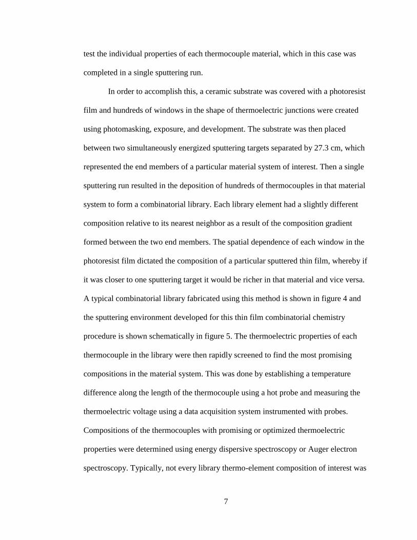
test the individual properties of each thermocouple material, which in this case was
completed in a single sputtering run.
In order to accomplish this, a ceramic substrate was covered with a photoresist
film and hundreds of windows in the shape of thermoelectric junctions were created
using photomasking, exposure, and development. The substrate was then placed
between two simultaneously energized sputtering targets separated by 27.3 cm, which
represented the end members of a particular material system of interest. Then a single
sputtering run resulted in the deposition of hundreds of thermocouples in that material
system to form a combinatorial library. Each library element had a slightly different
composition relative to its nearest neighbor as a result of the composition gradient
formed between the two end members. The spatial dependence of each window in the
photoresist film dictated the composition of a particular sputtered thin film, whereby if
it was closer to one sputtering target it would be richer in that material and vice versa.
A typical combinatorial library fabricated using this method is shown in figure 4 and
the sputtering environment developed for this thin film combinatorial chemistry
procedure is shown schematically in figure 5. The thermoelectric properties of each
thermocouple in the library were then rapidly screened to find the most promising
compositions in the material system. This was done by establishing a temperature
difference along the length of the thermocouple using a hot probe and measuring the
thermoelectric voltage using a data acquisition system instrumented with probes.
Compositions of the thermocouples with promising or optimized thermoelectric
properties were determined using energy dispersive spectroscopy or Auger electron
spectroscopy. Typically, not every library thermo-element composition of interest was
8
determined; however a statistically sufficient number of thermocouple compositions
were measured to model the full range of interest. Custom sputtering targets of the
most promising materials could then be made using powder processing techniques.
Powders of each end member material were combined in the appropriate ratio, mixed
in a ball mill for 24 h, uniaxially pressed, and sintered in a high temperature furnace.
The thermocouple geometry shown in figure 4 could be scaled up to something more
comparable to the dimensions of a gas turbine blade (figure 3). A flow chart of the
combinatorial chemistry procedure developed for the work in this thesis is shown in
figure 6. The combinatorial chemistry techniques detailed above were fundamental to
the success of optimizing thermocouple materials in the In2O3-SnO2 and CuO-In2O3
systems.

9
Figure 4. Combinatorial library fabricated by simultaneous sputtering from CuO and
In2O3 targets. A composition gradient (note the color change of the thermoelements
from left to right) was formed between the two targets resulting in the fabrication of
several hundred thermocouples with unique compositions in a single sputtering run.
10
Figure 5. Schematic of the thin film combinatorial sputtering setup. Both targets are
simultaneously energized with equal radio frequency power and the patterned
substrate is placed equidistant from each target. The pattern contains hundreds of
windows in a photoresist film, each with a different position relative to each target.
This results in a unique, position dependent composition formed in each window.
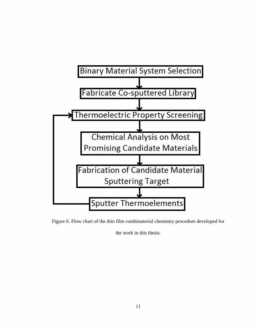
11
Figure 6. Flow chart of the thin film combinatorial chemistry procedure developed for
the work in this thesis.

12
1.3 Thermocouple testing
The thermocouples used to collect data for the manuscripts in chapters two and
four in this thesis were fabricated on ceramic beams using radio frequency sputtering
and tested using a custom tube furnace rig. The rig simulates the temperature gradient
impose along the length of the components inside the hot section of a gas turbine
engine. The rig use for the work in this thesis could achieve peak temperatures of
1400°C and differences as high as 1200°C along the length of the test beam. The hot
junction of the thin film thermocouple was placed inside the hot zone of a tube
furnace, a heat shield was placed just outside the hot zone and the cold junction was
clamped to an aluminum cooling block just outside the furnace. The aluminum block
was cooled with room temperature water to maintain the cold junction temperature
during thermal cycling of the furnace. Additional insulation of the cold junction was
provided by high temperature packing material. The custom tube furnace rig for
thermocouple testing is shown in panels of figure 7. This testing rig effectively placed
a temperature difference, from 0°C to 1200°C, along the length of the 7” beam, which
could be controlled by altering the 8” hot zone temperature of the furnace. The hot and
cold junction temperatures were monitored with commercial type-S and type-K wire
thermocouples, respectively, to continuously measure the temperature difference along
the beam. The thermoelectric voltage of each thin film thermocouple was collected
using a data acquisition system by attaching copper extension wires to the platinum
bond pads of each thermocouple using a conductive silver paste.
The thermoelectric properties of thermocouple library elements fabricated
using combinatorial chemistry were tested using a hot probe method. A temperature

13
Figure 7. Custom tube furnace testing rig for thin film thermocouples deposited on
ceramic beams, which applied a horizontal temperature difference along the length of
the thermocouple measured with type-K and type-S wire thermocouples. This setup
simulated the severe temperature gradients on the surface of components inside gas
turbine engine hot sections.
14
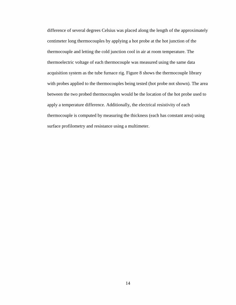
difference of several degrees Celsius was placed along the length of the approximately
centimeter long thermocouples by applying a hot probe at the hot junction of the
thermocouple and letting the cold junction cool in air at room temperature. The
thermoelectric voltage of each thermocouple was measured using the same data
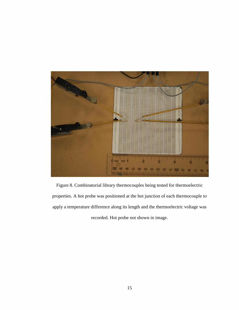
acquisition system as the tube furnace rig. Figure 8 shows the thermocouple library
with probes applied to the thermocouples being tested (hot probe not shown). The area
between the two probed thermocouples would be the location of the hot probe used to
apply a temperature difference. Additionally, the electrical resistivity of each
thermocouple is computed by measuring the thickness (each has constant area) using
surface profilometry and resistance using a multimeter.
15
Figure 8. Combinatorial library thermocouples being tested for thermoelectric
properties. A hot probe was positioned at the hot junction of each thermocouple to
apply a temperature difference along its length and the thermoelectric voltage was
recorded. Hot probe not shown in image.
16
CHAPTER 2
*STABILITY AND MICROSTRUCTURE OF INDIUM TIN OXYNITRIDE THIN
FILMS
2.1 Abstract
Indium oxide (In2O3) and indium tin oxide (ITO) thin films have been
investigated for high temperature thermocouple and strain gauge applications.
Reactive sputtering in nitrogen-rich plasmas was used to improve the high temperature
stability of indium oxide-based films in air and scanning electron microscopy was
used to follow the microstructural changes in the nitrogen-processed films. When
thermally cycled at temperatures above 800°C, a partially sintered microstructure
comprised of nanometer-sized crystallites was revealed. A densified layer was also
formed on the surface, which acted as an oxygen-diffusion barrier in the bulk film.
This combined with a network of partially sintered oxynitride crystallites lead to
considerable open porosity and a stabilizing effect on the ensuing electrical properties.
In this article, the thermoelectric properties of nitrogen-processed films were evaluated
at temperatures up to 1400°C. To study the effect of nitrogen plasma processing on the
sintering kinetics and associated densification, the constrained sintering of the
resulting films was followed as a function of time and temperature. Based on the
measured thermoelectric properties of the nitrogen processed films, drift rates on the
same order of magnitude as commercial type K wire thermocouples were realized for
these all-ceramic thermocouples.
*Gregory, Amani, Tougas, and Drehman, J. Am. Ceram. Soc., 95 [2], 705-710 (2012).
17
2.2 Introduction
Surface temperatures as high as 1500°C have been estimated for hot section
components in modern gas turbine engines, and when combined with the severe
thermal gradients often observed in these environments, modeling and simulation of
the thermo-mechanical behavior of these components becomes very difficult.
Therefore, direct temperature measurements are often necessary and thin film
thermocouples, in particular, offer a significant advantage over wire thermocouples in
such applications. Wire thermocouples are difficult to use for these measurements,
since they cannot be easily incorporated onto the surfaces of thermal barrier coatings
(TBC) deposited onto turbine blades, without affecting gas flow patterns.1 Thin film
thermocouples on the other hand can be directly deposited onto the surface of
components without the need for adhesives or surface preparation which can alter the
properties of the blades.2 Furthermore, thin films add negligible mass (micrograms) to
smaller turbine blades (grams) and have very fast response times (less than 1 μs).3
However, the materials used in traditional metallic thermocouples, including those
based on platinum and rhodium, suffer from reliability issues at temperatures above
900°C, such as selective rhodium oxidation. At these temperatures, the films are
susceptible to a variety of problems including selective rhodium oxidation, which can
cause the output of these devices to drift due to changes in composition. Furthermore,
this can result in thinning and poor adhesion due to dewetting of the film-to-oxide
surfaces. Platinum rhodium-based thermocouples also have very low output (on the
order of 12 μV/°C) and the output can be affected by the catalytic nature of platinum
18
in the presence of certain hydrocarbons, leading to measurement errors as large as
50°C.4,5
Due to the limitations of platinum and platinum:rhodium thermocouples,
several researchers have considered alternative materials for temperature measurement
in harsh environments. Studies using TiC–TaC thin film thermocouples by Bhatt et
al.6 yielded some promising results at temperatures as high as 1080°C however; these
devices were limited to operation in inert atmospheres or under vacuum conditions.
Devices based on MoSi2 and TiSi2 films have shown promise in air at temperatures as
high as 1200°C. The formation of a natural oxide with parabolic growth kinetics over
these silicide films protects them to very high temperatures, which is essential due to
the volatile nature of MoO3.7 However, to compensate for the loss of Si during
oxidation, an extra layer of Si must be deposited under the thermo-element. With the
added compensating layers, MoSi2 films were stable enough to be considered for RTD
applications. Unfortunately, the output of both silicide- and carbide-based
thermocouples is low, even compared to type S thermocouples.
Commonly used as transparent conducting electrodes in many electronic and
optoelectronic applications, In2O3 and In2O3:SnO2 (ITO) are wide band gap, oxide
semiconductors. At low concentrations of extrinsic dopants, charge carriers in these
transparent conducting oxides are usually attributed to oxygen vacancy defects
according to Eq. (1) below,
(1)
where
are doubly charged oxygen vacancies. Tin-doping of
In2O3 films has been used to dramatically improve the electrical conductivity, where

19
the substitution of two tin atoms and oxygen interstitial form a charge neutral carrier
site, in addition to self-doping caused by intrinsic defects. Since grain boundaries act
as impurity sinks, they play a critical role in the electrical conduction mechanism in
these films. Therefore, any changes in the grain boundary area per unit volume due to
sintering in these semiconductors will result in changes in the charge carrier
concentration and will eventually lead to drift.8
Aperathitis et al.9 have deposited films of indium oxynitride (InON) and
indium tin oxynitride (ITON) by reactively sputtering from oxide targets in Ar/N2
plasmas for optoelectronic applications. They concluded that increasing nitrogen
content in the plasma reduces the transparency and the carrier concentration in these
films. The ITON films have also been used for very high temperature thin film strain
gauges,10
which exhibited excellent piezoresistive response and very low drift rates at
temperatures above 1500°C. Recently, we demonstrated a stable, all-ceramic
thermocouple with a maximum operating temperature of 1250°C and an average
Seebeck coefficient of 170 μV/°C, which is more than an order of magnitude higher
than the output associated with metallic thermocouples that operate in the same
temperature range.11
In this study, thin film thermocouples were produced by reactive
sputtering from In2O3 and ITO targets in a nitrogen rich plasma, which dramatically
improved the stability, as indicated by the reduced hysteresis (upon heating/cooling)
and drift rates of these thermocouples at temperatures approaching 1400°C. The effect
of reactive sputtering on the stability of these films was monitored by measuring the
thermoelectric response, electrical resistivity, and the densification or shrinkage of the
film as a function of time and temperature.
20
2.3 Experimental Procedure
Thin film ceramic thermocouples were deposited by r.f. sputtering onto 190
mm 9 25 mm alumina substrates from In2O3, 95 wt% In2O3, 5 wt% SnO2 (ITO 95-5),
and 90 wt% In2O3, 10 wt% SnO2 (ITO 90-10) targets (Umicore Indium Products,
Providence, RI). The films were deposited using a MRC model 8667 and a MRC
model 822 sputtering system, where a total gas pressure of 1.33 Pa was maintained
during film deposition. The films were patterned by using conventional
photolithography techniques whereby windows were formed in a negative photoresist,
which have been used to pattern non-planar substrates such as turbine blades, and thus
all depositions were performed at room temperature. Platinum bond pads and
reference electrodes were sputtered from a high purity (99.99%) 100 mm diameter
platinum target at an r.f. power of 300 W, resulting in 1.5 μm thick films. All
thermoelectric testing done at temperatures in excess of 1200°C was performed using
platinum ink to form the hot junctions instead of platinum films, due to dewetting of
platinum under these conditions. All oxide films were deposited using the sputtering
parameters shown in Table 1 and had nominal thicknesses of 10–12 μm. Prior to
sputtering, a background pressure of less than 1 x 10⁻⁴
Pa was maintained in the
vacuum chamber, the respective targets were pre-sputtered onto shutters for 10 min to
remove surface contamination and release adsorbed water.
The thin film thermocouples were annealed at 500°C for 5 h in nitrogen,
followed by a second 2 h anneal at 1200°C. During testing in air, one end of the
thermocouples was placed into the hot zone of a tube furnace, to apply a temperature
difference along the length of the substrate. The temperature at the cold junction was

21
Sputtering
parameters Pt In2O3 InON ITON 95/5
ITON
90/10
Target diameter
(mm) 100 150 150 125 150
Power (W) 300 350 350 350 350
Power density
(W/cm2)
3.85 1.98 1.98 2.85 1.98
Sputtering gas
pressure
(Pa)
Ar:
1.33Pa
Ar: 1.33
Pa
Ar: 1.07 Pa
N2: 0.27 Pa
Ar: 1.07 Pa
N2: 0.27 Pa
Ar: 1.07
Pa
N2: 0.27
Pa
Deposition rate
(μm/hr) 0.6 1.2 1.1 0.9 1.4
Film thickness
(μm) 1.5
10.0 to
12.0 10.0 to 12.0 10.0 to 12.0
10.0 to
12.0
Table 1. Sputtering conditions of platinum, indium oxide and ITO films.
22
maintained at 20°C using an ethylene glycol coolant circulated through an aluminum
cooling block connected to a chiller. Both the hot and cold junction temperatures were
continuously monitored using type S and type K thermocouples, respectively. The
furnace was thermally cycled from room temperature to 1400°C at a heating/cooling
rate of 3°C/min. Long-term stability tests of the thermocouples were obtained by
testing the thermocouples for 200 h across a thermal difference of 1200°C. The
temperature coefficient of resistivity of the oxide and oxynitride films was determined
using the van der Pauw method. The sintering and growth kinetics of In2O3 films
sputtered in varying argon, oxygen and nitrogen partial pressures was measured using
a Dektak surface profilometer to determine the change in thickness of films, deposited
on highly polished alumina wafers as a function of time and temperature. These oxide
films were also grown on sapphire substrates and characterized using with grazing
incidence X-ray diffraction (GI-XRD) utilizing a CuKα radiation source.
2.4 Results and Discussion
The Seebeck coefficient in both degenerate and non-degenerate
semiconductors is highly dependent on the charge carrier concentration, ND.8 To
fabricate thermocouples with low drift rates, variations in ND must be minimized. As
grain boundaries act as impurity sinks, they play a critical role in the conduction
mechanism associated with transparent conducting oxides such as ITO.8 To obtain
stable thermoelectric responses, all thermocouples were heat-treated in N2 for 5 h at
500°C to eliminate point defects in the films, such as trapped argon and to improve the
electrical conductivity. Because the cold junction of the thermocouple is never

23
exposed to the peak operating temperatures of the device, inhomogeneities in the film
caused by compensation of oxygen vacancies in the hot junction can lead to noise,
drift and even voltage spikes. These were eliminated by heating the entire
thermocouple for 2 h in air at 1200°C. However, heat treatments cannot reduce drift in
the Seebeck coefficient caused by sintering of the materials in the hot junction.
Therefore, reduced sintering kinetics and oxygen diffusion barriers were employed to
improve the long-term performance of these ceramic thermocouples.
As nitride ceramics exhibit much slower sintering kinetics compared to oxide
ceramics,10
oxynitride thermoelements were prepared by reactively sputtering in
nitrogen-rich plasmas from In2O3 and ITO targets. This technique has been described
in the literature for ITO films heat-treated under various nitrogen partial pressures and
can lead to significant nitrogen incorporation into the films as well as a reduction in
the optical band gap and carrier concentration.12
Figure 9 shows the microstructure of
thermally cycled InON and In2O3 films. A network of submicrometer pores, capped
with a densified oxynitride layer was observed in the nitrogen processed films [Fig.
9(b)] which was not evident in the densified Ar processed film [Fig. 9(d)]. When
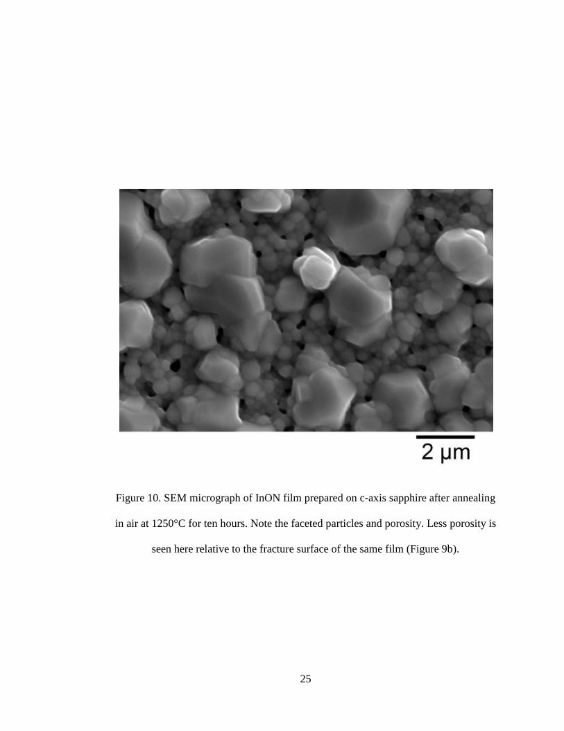
InON films were grown on a sapphire substrate (Fig. 10), relatively large (2–5 μm)
faceted crystallites were formed over a network of submicrometer grains. While this
also occurred to a lesser extent in InON films prepared on alumina substrates, these
features were only observed on the surface of the InON films and were not present in
any of the tin doped samples. The X-ray diffraction patterns of the In2O3-based films
grown on sapphire are shown in Fig. 11. When the In2O3 films were prepared in pure
argon, the (400) peak dominated the XRD pattern, suggesting that the films are highly
24
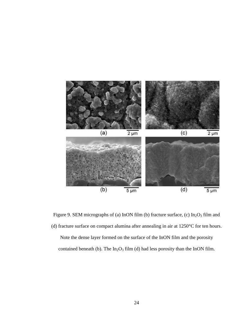
Figure 9. SEM micrographs of (a) InON film (b) fracture surface, (c) In2O3 film and
(d) fracture surface on compact alumina after annealing in air at 1250°C for ten hours.
Note the dense layer formed on the surface of the InON film and the porosity
contained beneath (b). The In2O3 film (d) had less porosity than the InON film.
25
Figure 10. SEM micrograph of InON film prepared on c-axis sapphire after annealing
in air at 1250°C for ten hours. Note the faceted particles and porosity. Less porosity is
seen here relative to the fracture surface of the same film (Figure 9b).
26
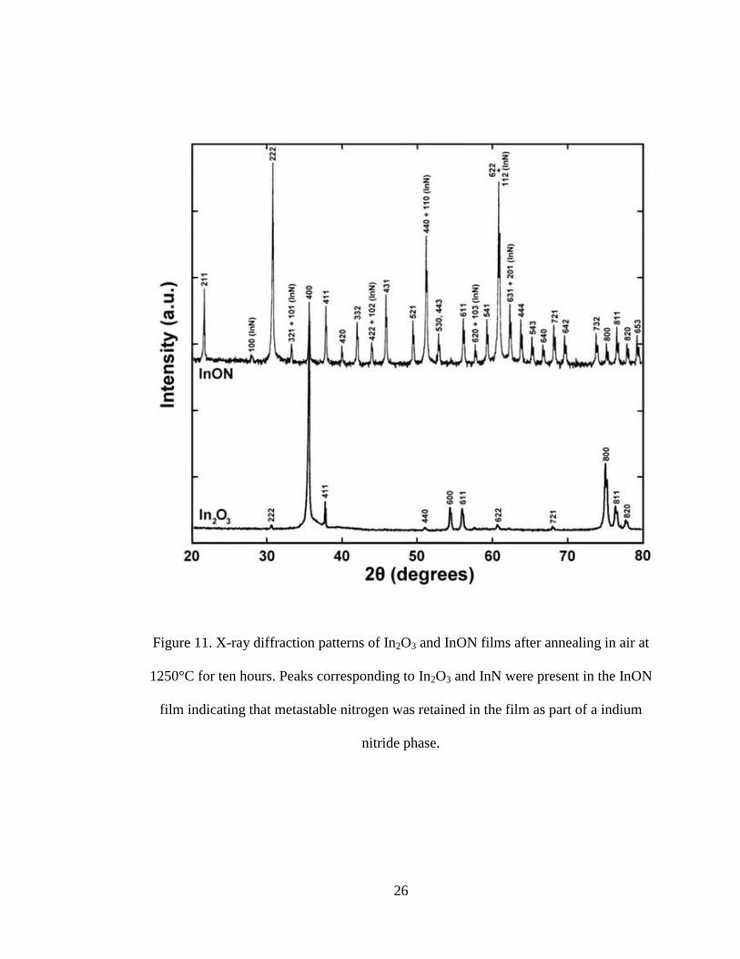
Figure 11. X-ray diffraction patterns of In2O3 and InON films after annealing in air at
1250°C for ten hours. Peaks corresponding to In2O3 and InN were present in the InON
film indicating that metastable nitrogen was retained in the film as part of a indium
nitride phase.
27
oriented. In the nitrogen-processed films, XRD peaks corresponding to both In2O3 and
InN were identified, and no preferred orientation was observed in these films. We
believe that the isolated crystallites observed on the surface were formed by a
vaporization–condensation mechanism, whereby the growth of InON was triggered by
the instability of sub-oxides of indium at low temperatures and oxygen-partial
pressures.13
This led to the formation of a densified, nonporous layer that can be seen
in the SEM fractographs in Fig. 9(b). A slight increase in the lattice spacing was also
observed in the InON films relative to the In2O3 films. A shift of 2.530 to 2.546 Å was
calculated for the (400) peak in these films. This shift has been previously documented
for ITON and other oxynitrides,9,14
and suggests that nitrogen was present in the
“bulk” film as well as in the densified layer.
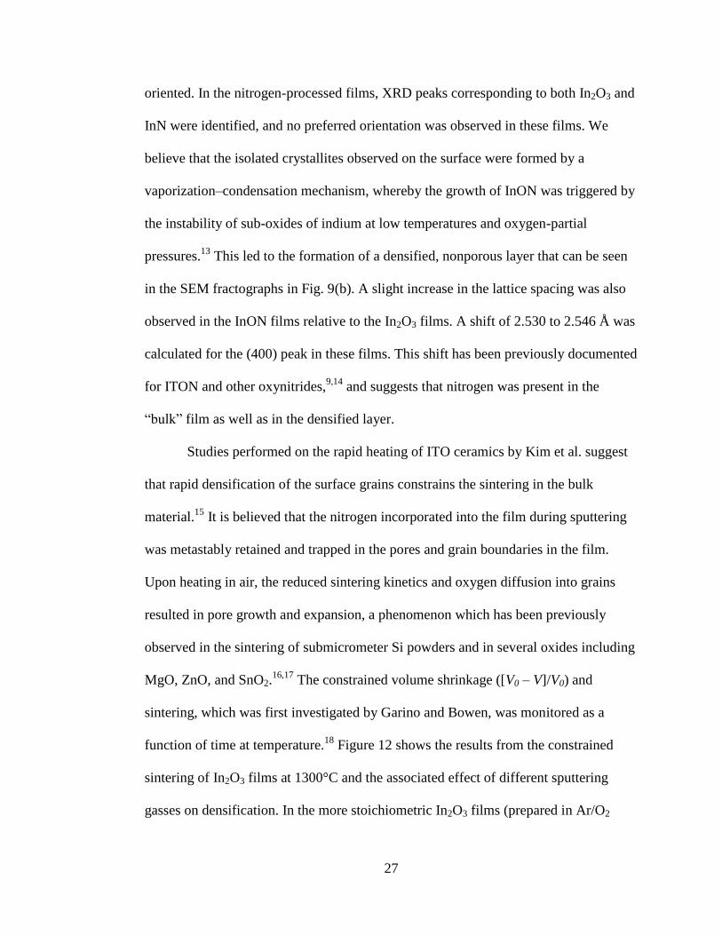
Studies performed on the rapid heating of ITO ceramics by Kim et al. suggest
that rapid densification of the surface grains constrains the sintering in the bulk
material.15
It is believed that the nitrogen incorporated into the film during sputtering
was metastably retained and trapped in the pores and grain boundaries in the film.
Upon heating in air, the reduced sintering kinetics and oxygen diffusion into grains
resulted in pore growth and expansion, a phenomenon which has been previously
observed in the sintering of submicrometer Si powders and in several oxides including
MgO, ZnO, and SnO2.16,17
The constrained volume shrinkage ([V0 – V]/V0) and
sintering, which was first investigated by Garino and Bowen, was monitored as a
function of time at temperature.18
Figure 12 shows the results from the constrained
sintering of In2O3 films at 1300°C and the associated effect of different sputtering
gasses on densification. In the more stoichiometric In2O3 films (prepared in Ar/O2
28
Figure 12. Isothermal constrained shrinkage ((V0-V)/V0) of In2O3 films prepared in Ar
(blue square), Ar/O2 (green circle) and Ar/N2 (red triangle) plasmas at 1300°C as a
function of time.
29
plasmas), sublimation was observed during heat treatments after rapid densification,
while no significant thickness changes were observed in films prepared in argon
plasmas. On the other hand, a 12% increase in volume was observed in the oxynitride
film after 2 h at temperature, consistent with a pore growth mechanism during
sintering.17
Prior to heat treatment in air, the In2O3 and ITO films behave like degenerate
semiconductors due to the very high concentration of defects in the film. After the
material had been heated in air, thermally activated oxygen diffusion resulted in partial
compensation of the doubly charged oxygen vacancies in the film. However, thermally
cycled In2O3 films remain relatively conductive at room temperature (with resistivities
as low as 0.02 Ω·cm) despite the compensated charge carriers. This is a result of the
film’s complex bixbyite crystal structure which contains unoccupied oxygen
interstitial positions.19
The temperature dependence of the electrical resistivity in ITO
films after heat treatments in air has been well documented and is known to have a
distinct transition corresponding to the excitation of all dopant species to the
conduction band, which occurs at temperatures between 600°C and 700°C.20
Thermally activated electrical conductivity was observed in these semiconductors and
is described by the following equation:
(2)
where k is Boltzmann’s constant, T is the absolute temperature, and ΔEa is the
activation energy, which is the energy gap between the conduction band edge and the
Fermi level. Arrhenius plots showing the electrical conductivity and activation energy
of both argon and nitrogen processed In2O3 and ITO films are displayed in Fig. 13.

30
Figure 13. Electrical resistivity of In2O3 and ITO films prepared in Ar and Ar/N2
plasmas.

31
The activation energies corresponding to temperatures above and below the transition
temperature are listed in Table 2. These results indicate that the oxynitride films have
significantly higher activation energies (~70% increase) than their oxide counterparts,
supporting the XRD results, that nitrogen is present in the bulk film, as well in the
densified layer. Nitrogen acts as a valence band acceptor in oxide semiconductors and
incorporation of nitrogen into the films results in a reduction of the Fermi energy,
which explains the shift in activation energy. In all cases, the oxynitride films were
more resistive than their oxide counterparts when measured at room temperature.
To investigate the effects of reactive sputtering on the thermoelectric power of
In2O3, several thermocouples were prepared in various argon, oxygen and nitrogen
partial pressures. These thermocouples were tested relative to platinum reference
electrodes, as shown in Fig. 14. Here, it was found that the films prepared in pure
argon and in oxygen rich plasmas had larger magnitude Seebeck coefficients than
those deposited in nitrogen-rich plasmas. For non-degenerate semiconductors such as
In2O3, the Seebeck coefficient described by,
(3)
where S is Seebeck, k is the Boltzmann constant, e is the electron charge, me* is the
effective mass, ħ is Planck’s constant, and A is a transport constant (typically 0 ≤ A ≤
4).21
For non-degenerate semiconductors, a decrease in the carrier concentration
increases the magnitude of the Seebeck coefficient. It is expected that the oxynitride
films will have a significantly reduced Seebeck coefficient since nitrogen acts as a
valence band acceptor in conducting oxides, making the thermoelectric power more

32
Target Material Oxide Film Oxynitride Film
T < 950 K T > 950 K T < 950 K T > 950 K
In2O3 5.86 meV 115 meV 8.68 meV 169 meV
ITO 95/5 16.1 meV 205 meV 25.1 meV 313.8 meV
ITO 90/10 13.5 meV 212 meV 21.3 meV 286 meV
Table 2. Activation energies associated with the electrical conductivities of various
oxide and oxynitride films as a function of thermal cycling.
33
Figure 14. Seebeck coefficient of In2O3 films prepared in Ar, Ar/N2, and Ar/O2
plasmas.
34
positive (smaller magnitude). The Seebeck coefficient of ITO on the other hand is
given by,
(4)
which is identical to the expression used for metals and is valid because the free
electron-like behavior observed in degenerate semiconductors, where A is a transport
constant that describes the predominant scattering process.8 Incorporation of nitrogen
into ITO has been shown to cause a reduction in carrier concentration as well as the
Fermi level due to an increase in activation energy and will therefore increase the
Seebeck coefficient of ITO.11
In the In2O3–ITO thermocouples fabricated by Chen et
al.,11
a degenerately doped n-type semiconductor with a very low Seebeck coefficient
was combined with a non-degenerate n-type semiconductor having a relatively high
Seebeck coefficient, which yielded thermoelectric powers greater than 150 μV/°C.
During the lifetime of these devices, significant changes in the microstructure were
observed, which led to large drift rates, which is defined according to Eq. (5) as,
(5)
By introducing nitrogen into the films, the thermoelectric powers of the non-
degenerate material were reduced and those of the degenerate material were increased.
This resulted in a reduction in the overall Seebeck coefficient of the oxynitride based
thermocouples. However, despite their lower thermoelectric output, the oxynitride
thermocouples had lower drift rates (Table 3). The long-term stability of these thin
film thermocouples was compared by computing their drift rates after 200 h of testing

35
V (ΔT) = A(ΔT)
3 +
B(ΔT)2+C(ΔT)
Thermocouple
Pair
A
(mV/°C3)
B
(mV/°C2)
C
(mV/°C)
Seebeck
Coefficient at
1200°C (μV/°C)
Drift
Rate
(°C/hr)
In2O3 vs. ITO
(95/5)
-6.90
× 10-7
1.44
× 10-4
7.27
× 10-2
170 3.76
In2O3 vs. ITO
(90/10)
-7.78
× 10-7
1.41
× 10-4
6.33
× 10-2
162 20.4
InON vs. ITON
(95/5)
-1.43
× 10-8
4.66
× 10-5
2.17
× 10-2
68 0.57
InON vs. ITON
(90/10)
-1.61
× 10-8
5.47
× 10-5
2.54
× 10-2
56 0.63
Table 3. Thermoelectric response and drift rate of In2O3 vs. ITO and InON vs. ITON
thin film thermocouples.
36
at a hot junction temperature of 1200°C. For comparison, a 0.5 mm diameter type K
wire thermocouple had a drift rate of 0.18 K/h at operating temperatures of 1100°C.22
Furthermore, the hysteresis in the thermoelectric output observed during rapid heating
and cooling cycles of the ceramic thermocouples (Fig. 15) was further reduced
through nitrogen processing. At temperatures above 1400°C, a loss of tin in the ITON
films was observed, ultimately resulting in device failure. However, the nitrogen-
processed InON films survive temperatures greater than 1500°C. The significant
improvements observed in the stability and hysteresis of the InON versus ITON
thermocouples make them much more suitable for high temperature measurements,
despite their relatively small thermoelectric outputs.
2.5 Conclusion
Ceramic thermocouples based on porous indium oxynitride and indium tin
oxynitride thin films were developed to replace noble metal thermocouples used to
measure temperatures in the hot section of gas turbine engines. Metastably retained
nitrogen was introduced into the films by reactive sputtering in nitrogen-rich plasmas
where, upon heating, the nitrogen becomes trapped in isolated pores with grain
boundaries affecting the solid/vapor equilibrium. Due to the reduced sintering kinetics
of nitride ceramics relative to oxide ceramics, the grain boundaries were stabilized to
very high temperatures. Since the Seebeck coefficient for both nondegenerate and
degenerate semiconductors is a function of the charge carrier concentration, a
significant reduction in the drift rate was observed for these oxynitride-based
thermocouples compared to thermocouples prepared in argon plasmas.

37
Figure 15. Thermoelectric output and hysteresis (heating: red, cooling: blue) of
ceramic thin film thermocouples.
38
List of References
1J. F. Lei and H. A. Will, "Thin-Film Thermocouples and Strain-Gauge Technologies
for Engine Applications", Sensors and Actuators A, 65 (1998) 187-193.
2L. C. Martin and R. Holanda, “Applications of Thin Film Thermocouples for Surface
Temperature Measurement”, NASA TM-106714, (1994).
3H. Choi and X. Li, "Fabrication and application of micro thin film thermocouples for
transient temperature measurement in nanosecond pulsed laser micromachining of
nickel", Sensors and Actuators A, 136 (2007) 118-124.
4G. E. Aniolek and O. J. Gregory, "Thin film thermocouples for advanced ceramic gas
turbine engines", Surface and Coatings Technology, 68-69 (1994) 70-75.
5K. G. Kreider, "Sputtered high temperature thin film thermocouples", Journal of
Vacuum Science Technology, 11 (1993) 1401-1405.
6K. Ellmer and R. Mientus, “Carrier transport in polycrystalline ITO and ZnO:Al II:
The influence of grain barriers and boundaries”, Thin Solid Films, 516 (2008) 5829-
5835.
7E. Aperathitis, M. Bender, V. Cimalla, G. Ecke, and M. Modreanu, “Properties of rf-
sputtered indium-tin-oxynitride thin films”, Journal of Applied Physics, 94 (2003) [2]
8O.J. Gregory and T. You, “Piezoresistive Properties of ITO Strain Sensors Prepared
with Controlled Nanoporosity”, Journal of the Electrochemical Society, 151 (2004) (8)
H198-H203
9X. Chen, O.J. Gregory, and M. Amani, “Thin-Film Thermocouples Based on the
System In2O3-SnO2”, Journal of the American Ceramic Society, 94 (2011) [3] 854-860

39
10E. Aperathitis, M. Modreanu, M. Bender, V. Cimalla, G. Ecke, M. Androulidaki, and
N. Pelekanos, “Optical characterization of indium-tin-oxynitride fabricated by RF-
sputtering”, Thin Solid Films, 450 (2004) 101-104
11E. Medvedovski, C. J. Szepesi, O. Yankov, and P. Lippens, “Indium tin oxide
nanosized transparent conductive thin films obtained by sputtering from large size
planar and rotary targets”, Ceramic Transactions, 223 (2010) 125-146
12B. C. Kim, J. H. Lee, J. J. Kim, and T. Ikegami, “Rapid rate sintering of
nanocrystalline indium tin oxide ceramics: particle size effect”, Materials Letters, 52
[1-2] (2002) 114-119
13O. J. Gregory, S. B. Lee, R. C. Flagan, “Reaction Sintering of Submicrometer
Silicon Powder”, Journal of the American Ceramic Society, 70 (1987) [3] C52-C55
14J.A. Varela, O.J. Whittemore, E. Longo, “Pore size evolution during sintering of
ceramic oxides”, Ceramics International, 16 (1990) [3] 177-189
15T. J. Garino and H. K. Bowen, “Kinetics of Constrained-Film Sintering”, Journal of
the American Ceramic Society, 73 (1990) [2] 251-257
16S.P. Harvey, T.O. Mason, Y. Gassenbauer, R. Schafranek, and A. Klein, “Surface
versus bulk electronic/defect structures of transparent conducting oxides: I. Indium
oxide and ITO”, Journal of Physics D: Applied Physics, 39 (2006) 3959-3968
17O. J. Gregory, Q. Luo, and E. E. Crisman, "High Temperature Stability of Indium
Tin Oxide Thin Films", Thin Solid Films, 406 (2002) 286-293.
18G. Jonker, “The Application of Combined Conductivity and Seebeck-Effect Plots for
the Analysis of Semiconductor Properties”, Philips Research Report, 23 (1968) [2]
131-138

40
19R. E. Bentley, “Handbook of Temperature Measurement Vol. 3: Theory and Practice
of Thermoelectric Thermometry”, Springer, 1998.
41
CHAPTER 3
*THERMOELECTRIC PROPERTIES AND MICROSTRUCTURE OF Cu-In-O
THIN FILMS
3.1 Abstract
Combinatorial chemistry techniques were used to study the thermoelectric
properties of sputtered thin films in the system copper oxide (CuO) and indium oxide
(In2O3). Hundreds of thin film thermocouples or combinatorial library elements were
simultaneously deposited, each with a unique spatially dependent chemistry. The
resulting thermoelectric properties of each element were determined along with
electrical resistivity as a function of composition. Energy dispersive spectroscopy was
used to identify the composition of each thermo-element and electron and x-ray
diffraction were used to determine the degree of crystallinity and phases present.
Transmission electron microscopy was used to characterize the microstructure of
selected thermo-elements. A change in sign of the thermoelectric voltage was
observed in the thermo-element containing 40 atomic percent indium, which suggests
a change in the dominant carrier type occurred, from p-type to n-type. Based on this
finding, the fabrication of thermoelectric p-n junctions using the same base Cu-In-O
semiconductor appears feasible.
*Gregory, Tougas, Amani, and Crisman, J. Electron. Mater., in press (2013).
42
3.2 Introduction
Transparent conducting oxides (TCO) based on the material system Cu-In-O
have been considered for applications such as flat panel displays, solar cells, and thin
film transistors [1, 2]. However, there have been relatively few studies of the
thermoelectric properties of such materials to date [3]. Recently, considerable efforts
have focused on the thermoelectric properties of oxides for applications such as
energy harvesting, and power generation [4-7]. Compared with more conventional
thermoelectric materials, oxides offer dramatically improved chemical stability in air,
inherently higher carrier concentrations, and can be used at significantly higher
temperatures. Both, indium oxide (In2O3), an n-type semiconductor, and In2O3 doped
with +4 cations has shown promise as a thermoelectric material [3, 4]. Copper oxide
(CuO), a p-type semiconductor, has been considered for thermoelectric applications
but has a relatively small band gap (1.2 eV) compared to In2O3 [8], which limits its
use in high temperature thermoelectric applications. Furthermore, CuO changes
oxidation state as a function of temperature [9, 10]. However, alloys comprised of
CuO and In2O3 typically exhibit larger band gaps (on the order of 3eV) than the stand-
alone materials, making them more suitable for thermoelectric applications.
The delafossite (Cu+1
In+3
O2) phase in the Cu-In-O system has received
considerable attention for TCO applications [11-13]. This material can be “tuned” in
such a way that either p-type or n-type carriers can dominate; e.g. by substituting Sn+4
for indium or Ca+2
for copper [12, 14]. The formation of this phase, or this phase with
the inclusion of dopants, requires careful processing routes. These routes have been
demonstrated successfully in previous studies [14, 15]. However, few if any studies
43
have focused on tuning the composition of the Cu-In-O compounds to achieve p-type
or n-type dominant carriers in the base compound without the need for doping.
In this study, combinatorial chemistry techniques were used to fabricate thin
film thermo-elements based on Cu-In-O prepared by sputtering from CuO and In2O3
targets. By combining a p-type semiconductor (CuO) with an n-type semiconductor
(In2O3), thin film thermo-elements with either p-type or n-type character could be
produced without relying on synthesizing the p-type or n-type auto-doped CuInO2
phase. The library thermo-elements were largely amorphous and each was catalogued
according to the atomic percentage of indium in the film. The relation between the
library element composition and the dominant carrier type was characterized using the
hot probe method. A transition from p-type to n-type conduction in the Cu-In-O
system was observed at a film composition of 40 at% indium. Energy dispersive
spectroscopy (EDS) was used to determine the composition of each thermo-element
and the microstructures of as-deposited and annealed thermo-elements were
characterized using transmission electron microscopy (TEM). Electron diffraction in
conjunction with TEM and x-ray diffraction (XRD) were used to determine the extent
of crystallinity and the distribution of phases in select library thermo-elements.
3.3 Experimental Procedure
Cu-In-O films were deposited onto high purity alumina substrate and oxidized
silicon wafer by co-sputtering from CuO and In2O3 targets to form a combinatorial
library containing thermo-elements in the Cu-In-O system. Prior to deposition,
reference electrodes (complementary thermocouple leg to Cu-In-O thermo-element)

44
were fabricated using photolithography in conjunction with lift-off. Platinum,
sputtered in ultra high purity (UHP) argon at 9 mT, was deposited as the reference
electrode material. A photolithographic step was used to create 770 Cu-In-O thermo-
elements with each thermo-element at different position relative to the two sputtering
targets. The sputtering targets were six inches in diameter and were spaced 27.3 cm
apart. A radio frequency power of 200 W was fed continuously to each sputtering
target during deposition. In this way, a chemical composition gradient was established
in the thermo-elements along the axis between the targets and a thickness gradient was
established in the orthogonal direction. The resulting thermocouples formed an array
suitable for rapid thermoelectric property screening.
All thermocouples were subsequently annealed in nitrogen at 400°C for five
hours to release trapped argon and densify the thermo-elements. Final film thicknesses
ranged from 1 to 2 μm. Thermoelectric data were obtained from the library
thermocouples deposited on an alumina substrate, after a temperature difference was
established between the hot and cold junctions. Each thermo-element was typed p- or
n- based on the voltage sign relative to the platinum reference electrode. Voltages
were recorded using an iOTech USB data acquisition system and Personal Daq View
Plus© software. Thin film type-K thermocouples were deposited, by sputtering from
alumel and chromel targets in 9 mT Ar, at the hot and cold junction of a thermocouple
with the same geometry as the library thermocouples to calibrate the temperature
difference across the junction. Electrical resistivity was measured on films deposited
on the oxidized surface of a silicon wafer after the thermocouples were nitrogen
annealing. The composition of each thermo-element in the library array was

45
determined with EDS measurements on a JEOL-5900 SEM. The microstructures of
select library thermo-elements were examined in a JEOL JEM-2100 TEM by
depositing films directly onto silicon nitride grids. The thin films were examined as-
deposited, after a 400 °C, 5 h nitrogen anneal, and after repeating the nitrogen anneal
another 5 h at 400 °C. A Rigaku Ultima-IV XRD system was used to determine the
degree of crystallinity and distribution of phases present in selected thermo-elements.
3.4 Results and Discussion
3.4.1 Thermoelectric Properties
The thermoelectric voltages of the Cu-In-O combinatorial library thermo-elements are
summarized in Figure 16, which shows thermoelectric voltage as a function of
position. By comparing the thermoelectric voltage and spatial distribution of the
chemical composition, maps of thermoelectric voltage and resistivity as a function of
composition were generated (Figure 17). Figure 17a shows a continuous transition
from n- to p- conduction occurring at a film composition of 40 at% indium. The CuO-
In2O3 phase regions were superimposed over the data in Figure 17a. It indicates that
the n- to p- transition occurs in a copper rich film, which falls within a two phase
region of CuO and Cu2In2O5. Since the films studied are largely amorphous, we
suggest that a doping effect from the copper was responsible for the observed p-type
behavior in the copper rich films rather than from the formation of different phases in
the material as the copper content was increased. Figure 17b indicates that little
variation in the electrical resistivity was observed for thermo-elements containing

46
Figure 16. Map of the thermoelectric voltage as a function of composition (at%
indium) for nitrogen annealed combinatorial library (a temperature difference of T =
7.7 °C was applied across individual thermocouples).
47
Figure 17. Plots of (a) thermoelectric voltage and (b) electrical resistivity of Cu-In-O
films as a function of composition (at% indium) and phase region. Dashed line
presented is a guide for the eye to see the p-n transition composition indicated by a
change in the sign of the thermoelectric voltage. Red line represents the single phase
composition Cu2In2O5. The CuO and Cu2In2O5 phase region is to the left of the red
line and the Cu2In2O5 and In2O3 phase region is to the right of the red line [10].
48
25-45 at% indium. However, the thermoelectric response changed by nearly 3 mV
over the same range. This phenomenon was likely due to the increased copper oxide
content in the films as the indium content was varied from 45 at% to 25 at%. Also
apparent in figures 17a and b are horizontal “flat” regions (<15 at% and >75 at%
indium) over which reliable thermoelectric measurements could not be obtained
because of the high electrical resistivity of the thermo-elements in these composition
ranges. Peak thermoelectric voltages for the library thermo-elements exhibiting p-type
behavior and n-type behavior occurred between 20-25 at% indium and 50-60 at%
indium, respectively. Plots of resistivity as a function of composition (figure 17b)
clearly show two minima at 25-30 at% indium and 55-60 at% indium, which are the
same compositional ranges as the p-type and n-type materials with the largest
thermoelectric responses. It is important to note here that the thermo-elements were
not heated in air and thus the use of Cu-In-O thermoelectric materials in oxidizing
ambient may be limited.
3.4.2 Crystallography and Phases
XRD patterns of four nitrogen annealed Cu-In-O thermo-elements grown on
sapphire substrates are shown in Figure 18. The two copper rich films (35 at% In and
28.5 at% In) exhibited a low intensity CuO {111} peak and no other peaks were
observed. As the indium oxide content in the thermo-elements increased (61 at% In,
45.5 at% In), the degree of crystallinity increased as determined by peaks
corresponding to Cu2In2O5 and In2O3 phases. Typically, films in the Cu-In-O system
grown at or near room temperature are largely amorphous or have significant
amorphous regions [11], which was clearly evident in the copper rich films. However,
49
the indium oxide rich thermo-elements had well defined crystalline phases, although
many of the additional peaks were low in intensity. The presence of CuO, Cu2In2O5,
and In2O3 phases as a function of composition was in close agreement with the phase
diagram for the CuO-In2O3 system [10]. The investigators established the phase
diagram by combining CuO and In2O3 in various ratios, sintering them in air, and
determining the resulting phase distribution by XRD. The thermo-elements fabricated
in the present study were annealed in nitrogen and remained consistent with the phase
diagram for this system up to high temperatures in an inert environment such as argon
or nitrogen [10].
3.4.3 Microstructure
TEM was used to follow microstructural changes of selected elements from the
combinatorial library as a function of heat treatment. The TEM images of various Cu-
In-O elements are shown in figures 19 and 20. The electron diffraction patterns of the
as-deposited films indicated they were amorphous with little or no fine structure
(figure 19a). Annealing of the indium oxide rich films (> 40 at% In) resulted in the
formation of small crystallites in an amorphous matrix. As the copper oxide content
was systematically increased (< 40 at% In), relatively large, faceted particles were
observed (figures 19e & 20a). EDS analysis of those dispersed particles indicated that
they have increased oxygen and copper content relative to the surrounding matrix. At
lower magnification, figure 20a shows phase separation of highly crystalline, copper
oxide particles (dark) against a distinct lighter background matrix. The lighter phase
was further magnified to disclose a copper oxide rich phase (light) and indium oxide
50
Figure 18. XRD patterns of four Cu-In-O films; three copper oxide rich at 28.5 at% In
and 35 at% In and 45.5 at% In and one indium-rich at 61 at% In.

51
Figure 19. TEM micrographs and electron diffraction patterns for: (a, b) typical as
deposited films showing totally amorphous and uniform structure, (c, d) at onset of
crystallinity (after 400 °C, 5 h nitrogen anneal), and (e, f) after phase separation of the
film into large copper-rich particles.
52
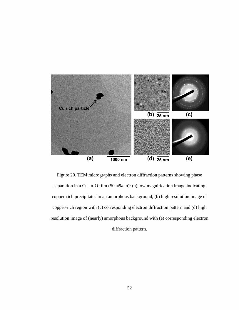
Figure 20. TEM micrographs and electron diffraction patterns showing phase
separation in a Cu-In-O film (50 at% In): (a) low magnification image indicating
copper-rich precipitates in an amorphous background, (b) high resolution image of
copper-rich region with (c) corresponding electron diffraction pattern and (d) high
resolution image of (nearly) amorphous background with (e) corresponding electron
diffraction pattern.
53
rich phase (dark) as shown in figures 20b and 20d, respectively with corresponding
electron diffraction patterns in figures 20c and 20e. Preferred orientation of the matrix
tends to increase as the amount of copper in the thermo-element was increased (figures
19f and 20c). This contrasts with the XRD spectra from above because these same
copper rich thermo-elements were amorphous. This was due to the relative size scale
at which these measurements were taken. The TEM images corresponded to a much
smaller area of the thermo-elements than that examined using XRD. Therefore,
variations in the thermo-element crystallinity are prevalent.
3.5 Conclusion
The Cu-In-O thermo-elements with the largest p-type and n-type response are
promising candidates for further consideration as thermoelectric materials. Cu-In-O p-
n junctions can be fabricated for thermoelectric applications such as thermoelectric
generators by sputtering thermo-elements from targets of the same compositions as the
best performing p-type and n-type materials to form thermocouples. Additionally, the
p-type and n-type thermo-elements will be compatible in terms of thermal expansion
during thermal cycling since they are from the same materials system.
54
List of References
1C. G. Granqvist, Solar Energy Materials and Solar Cells, 91, 1529 (2007).
2K. Nomura, H. Ohta, A. Takagi, T. Kamiya, M. Hirano, H. Hosono, Nature, 432, 488
(2004).
3D. Bérardan, E. Guilmeau, A. Maignan, and B. Raveau, Journal of Applied Physics,
104, 064918 (2008).
4E. M. Hopper, Q. Zhu, J-H Song, H. Peng, A. J. Freeman, and T. O. Mason, Journal
of Applied Physics, 109, 013713 (2011).
5D. Bérardan, E. Guilmeau, A. Maignan, and B. Raveau, Solid State Communications,
146, 97-101 (2008).
6H. Kaga, R. Asahi, and T. Tani, Japanese Journal of Applied Physics, 43 (6a), 3540-
3543 (2004).
7M. Amani, I. M. Tougas, O. J. Gregory, and G. C. Fralick, Journal of Electronic
Materials, 42 (1), 114-120 (2013).
8M. Yin, C-K. Wu, Y. Lou, C. Burda, J. T. Koberstein, Y. Zhu, and S. O’Brien,
Journal of the American Chemical Society, 127 (26), 9506-9511 (2005).
9J-C Lee, Y-W Heo J-H Lee, and J-J Kim, Thin Solid Films, 518, 1234 (2009).
10M. Bosacka, E. Filipek, P. Šulcova, Ž. Dohnalová, and A. Paczesna, Journal of
Thermal Analysis and Calorimetry, 109, 605-610 (2012).
11A. V. Chadwick, A. N. Blacklocks, A. Rougier, and C. Yaicle, Journal of Physics:
Conference Series, 249, 012045 (2010).
12H. Kawazoe, M. Yasukawa, H. Hyodo, M. Kurita, H. Yanagi, and H. Hosono,
Nature, 389, 939 (1997).
55
13L. Liu, K. Bai, H. Gong, and P. Wu, Chemistry of Materials, 17, 5529-5537 (2005).
14H. Yanagi, T. Hase, S. Ibuki, K. Udea, and H. Hosono, Applied Physics Letters, 78,
1583 (2001).
15M. Shimode, M. Sasaki, and K. Mukaida, Journal of Solid State Chemistry, 151, 16
(2000).
56
CHAPTER 4
THIN FILM PLATINUM-PALLADIUM THERMOCOUPLES FOR GAS TURBINE
ENGINE APPLICATIONS
4.1 Abstract
Thin film platinum:palladium thermocouples were fabricated on alumina and
mullite surfaces using radio frequency sputtering and characterized after high
temperature exposure to oxidizing environments. The thermoelectric output,
hysteresis, and drift of these sensors were measured at temperatures up to 1100 °C.
Auger electron spectroscopy was used to follow the extent of oxidation in each
thermocouple leg and interdiffusion at the metallurgical junction. Minimal oxidation
of the platinum and palladium thermoelements was observed after high temperature
exposure, but considerable dewetting and faceting of the films was observed in
scanning electron microscopy. An Arrhenius temperature dependence on the drift rate
was observed and later attributed to microstructural changes during thermal cycling.
The thin film thermocouples, however, did exhibit excellent stability at 1000 °C with
drift rates comparable to commercial type-K wire thermocouples. Based on these
results, thin film thermocouples based on platinum:palladium have considerable
potential for use in the hot sections of gas turbine engines.
Tougas and Gregory, Thin Solid Films, in press (2013).

57
4.2 Introduction
Gas turbine engine components based on advanced ceramics such as ceramic
matrix composites have superior thermomechanical properties at temperatures above
1000 °C when compared to conventional superalloys [1]. Additionally, ceramic
thermal barrier coatings have enabled gas turbine engine blades comprised of
superalloys to operate at temperatures as high as 1500 °C [2], which translates into
both improved fuel efficiency and reduced NOx emissions. Due to the severe
temperature gradients that can exist in these advanced materials, there is a need to
integrate sensors into these components to monitor their thermomechanical behavior.
Thin film sensors can be directly deposited onto both stationary and rotating engine
components for health monitoring as well as to verify existing models [1-3].
Thin film thermocouples offer several advantages over conventional wire
thermocouples or thermal spray instrumentation used in gas turbine engine
applications. Thin film sensors do not adversely affect gas flow patterns through the
engine since their thicknesses are well below the boundary layer thickness formed on
rotating surfaces [3, 4]. Thin film sensors also have negligible mass and therefore have
minimal effect on the vibrational modes of rotating components [5]. They are more
accurate and have faster response times than conventional wire sensors (< 1 μs) due to
their lower thermal mass. Additionally, thin films are not affected by the g forces
acting on the blades which are rotating at high velocities [3, 6]. Furthermore, the films
can be directly deposited onto the surface of engine components without the need for
adhesives, permitting more accurate surface temperature measurements than wire
based sensors [3].
58
Wire thermocouples have been employed in engine applications for more than
30 years, however, the presence of oxygen can cause instability and drift at
temperature in metallic thin film thermocouples due to the significantly reduced
diffusional distances in these devices. For example, conventional type-S thin film
(platinum:90 % platinum-10 % rhodium) thermocouples can suffer from selective de-
alloying of rhodium in the film due to the formation of rhodium oxides at temperatures
between 600-800 °C [7]. This results in a progressive, time dependent degradation or
drift in the thermoelectric output by as much as 5 °C/h as the platinum-rhodium
thermocouple legs undergo microstructural and compositional changes due to this
selective oxidation [3]. This effect can be mitigated by applying alumina overcoats to
protect the thermocouple elements from oxidation [3, 7]. Therefore, there is a need for
more stable thermocouple materials that do not experience detrimental microstructural
changes and selective oxidation issues at high temperature without resorting to
protective overcoats.
Platinum-rhodium alloys are currently being employed as complementary
thermoelements for wire-based thermocouples and thin film-based thermocouples.
However, noble metals such as gold, palladium, and platinum do not suffer from
selective oxidation processes at elevated temperatures since they are not alloys.
Unfortunately, the use of gold for high temperature thermocouple applications above
1000 °C is limited due to its low melting point (1064 °C) and dewetting of the metal
on oxide substrates at temperatures of 900 °C [8]. Wire thermocouples based on
platinum and palladium have been investigated to some extent [9-13], however,
investigations of thin film platinum:palladium thermocouples have been somewhat
59
limited. Kreider et al. has examined the use of thin film platinum:palladium
thermocouples on oxidized silicon wafers for radiometric temperature measurements
up to 1050 °C [14, 15]. However, these thermocouples could only measure
temperatures up to 850 °C and required the use of a titanium bond coat between the
silicon wafer and thermocouple elements due to dewetting issues [14, 15]. The use of
thin film platinum:palladium thermocouples for higher temperature applications has
not been previously investigated.
In this study, platinum:palladium thin film thermocouples were deposited onto
ceramic substrates, including alumina and mullite, using r.f. sputtering. The
thermoelectric output and drift were measured at temperatures up to 1100 °C and these
thin film thermocouples exhibited remarkable stability at high temperature in an
oxidizing environment. Auger electron spectroscopy (AES) was used to characterize
the chemical composition of the metallurgical junctions as a function of depth and to
monitor the extent of oxidation of the junction. The microstructure of the
thermocouple legs and metallurgical junctions were examined using scanning electron
microscopy (SEM).
4.3 Experimental details
Both alumina and mullite (CoorsTek, Inc.) were employed as the substrates for
all thin film platinum:palladium thermocouples. The substrates (190 mm x 25 mm x 2
mm) were cleaned with acetone, methanol, and deionized water. A dry film negative
photoresist (DuPontTM
MX 5050TM
) was applied to the surface of the substrates and
was soft-baked prior to patterning thin film thermocouples. After application of the
60
photoresist, the thin film thermocouple patterns were transferred to the resist using an
Optical Associates, Inc. aligner (350 nm wavelength ultraviolet light) to expose the
resist. The photoresist coated substrates were developed to reveal the desired pattern
and placed inside a Materials Research Corporation model 8667 sputtering system to
deposit the metal thermocouple legs. Platinum and palladium films were deposited in
pure argon. A background pressure of 2.7x10⁻⁴
Pa was achieved in the sputtering
chamber prior to sputtering and the stage (work piece) was maintained at temperatures
below 100 °C using water-cooling. Table 4 lists the sputtering parameters employed to
deposit the platinum and palladium films. Deposition resulted in 1.5 μm of platinum
and 2 μm of palladium.
All thin films were annealed in nitrogen for 5 h at 500 °C to remove point
defects, including trapped argon, and densify the films. The thermoelectric output was
measured as a function of time and temperature by placing the metallurgical junction
(hot junction) in the hot zone of a tube furnace and attaching the cold junction to an
aluminum chill block outside the furnace. In this way, a temperature difference was
applied along the length of the beam and the cold junction was maintained at or below
100 °C using chilled water. The thermocouples were thermally cycled in air to 900 °C
at 4 °C/min for several cycles to determine the thermoelectric voltage and the drift rate
was determined at 800 °C, 900 °C, 1000 °C, and 1100 °C over a 10 h period at each
temperature. The temperature difference was continuously monitored using type-K
(cold junction) and type-S (hot junction) wire thermocouples and copper extension
wires were attached to the bond pads of the platinum:palladium thermocouples using a
silver paste to acquire the voltage signals. All copper wires and wire thermocouples
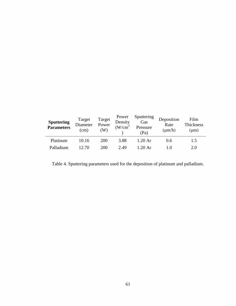
61
Sputtering
Parameters
Target
Diameter
(cm)
Target
Power
(W)
Power
Density
(W/cm2
)
Sputtering
Gas
Pressure
(Pa)
Deposition
Rate
(μm/h)
Film
Thickness
(μm)
Platinum 10.16 200 3.88 1.20 Ar 0.6 1.5
Palladium 12.70 200 2.49 1.20 Ar 1.0 2.0
Table 4. Sputtering parameters used for the deposition of platinum and palladium.
62
were connected to an IOTech Personal Daq 54 USB data acquisition system with
PDaq View Plus© software recording the temperature and voltage signals. AES depth
profiles were used to determine the chemical composition of the metallurgical junction
and identify oxidation products formed on the platinum and palladium thermocouple
legs. AES was performed using a Perkin Elmer 5500 Multi-Technique Surface
Analyzer. A background pressure of 6.0x10⁻⁷
Pa was established and a 1x1 mm area
on the surface of each thermocouple sample was sputter cleaned for 10 seconds prior
to acquiring each depth profile. SEM was performed on the same films to analyze the
microstructure after thermal cycling using a JEOL JSM-5900LV SEM and a 20 kV
accelerating voltage.
4.4 Results and Discussion
4.4.1 Thermoelectric measurements
The thermoelectric response of several platinum:palladium thin film
thermocouples are shown in Fig. 21a and Fig. 21b. A peak temperature of 900 °C was
employed at the hot junction during thermal cycling and a temperature difference as
large as 750 °C was established along the length of the ceramic substrates. The
maximum thermoelectric voltage of thin film thermocouples subjected to a
temperature difference of 750 °C was 9.00 mV on alumina substrates and 9.52 mV on
mullite substrates. This thermoelectric response was comparable to a conventional
type-S wire thermocouple, which typically has a thermoelectric response of 8.45 mV,
when a similar temperature difference is applied [16]. Remarkable stability was
observed for the thin film platinum:palladium thermocouples when tested over several
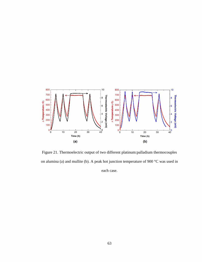
63
Figure 21. Thermoelectric output of two different platinum:palladium thermocouples
on alumina (a) and mullite (b). A peak hot junction temperature of 900 °C was used in
each case.
64
thermal cycles. However, the peak thermoelectric voltage at 900 °C for the thin film
thermocouples diminished slightly after each temperature ramp, which most likely
results from microstructural changes such as grain growth, pore growth, and dewetting
of the metallic films. Hysteresis upon heating and cooling to 900 °C is shown in Fig.
22. Here, the thin film thermocouples on mullite exhibited greater hysteresis than
those formed on alumina. However, the hysteresis was comparable to that of
previously studied ceramic thin film thermocouples deposited on alumina [2].
Furthermore, ceramic films have inherently greater stability in air because they have
all the oxygen that they can take in their structures.
The Seebeck coefficient and drift rates of the thin film thermocouples were
determined as a function of hot junction temperature and time, respectively. The
Seebeck coefficient defined in this study is given by Eq. 1
(1)
where S is the Seebeck coefficient given in μV/°C, is the voltage potential
difference between the two thermocouple materials ( ), and is the
temperature difference between the hot junction ( ) and the cold junction ( ). Eq. 2
gives the temperature dependence of the Seebeck coefficient for metal thermocouples
(2)
where is the carrier concentration, is the Boltzmann constant, is the effective
electron mass, is the absolute temperature, is the electron charge, and is a
transport constant [2]. There is no appreciable change in the carrier concentration of
these highly conductive platinum and palladium films over the temperature range of

65
Figure 22. Hysteresis upon heating/cooling platinum:palladium thermocouples on
alumina and mullite. Corresponds to second cycle of thermoelectric data in Figure 21a
and Fig. 21b.
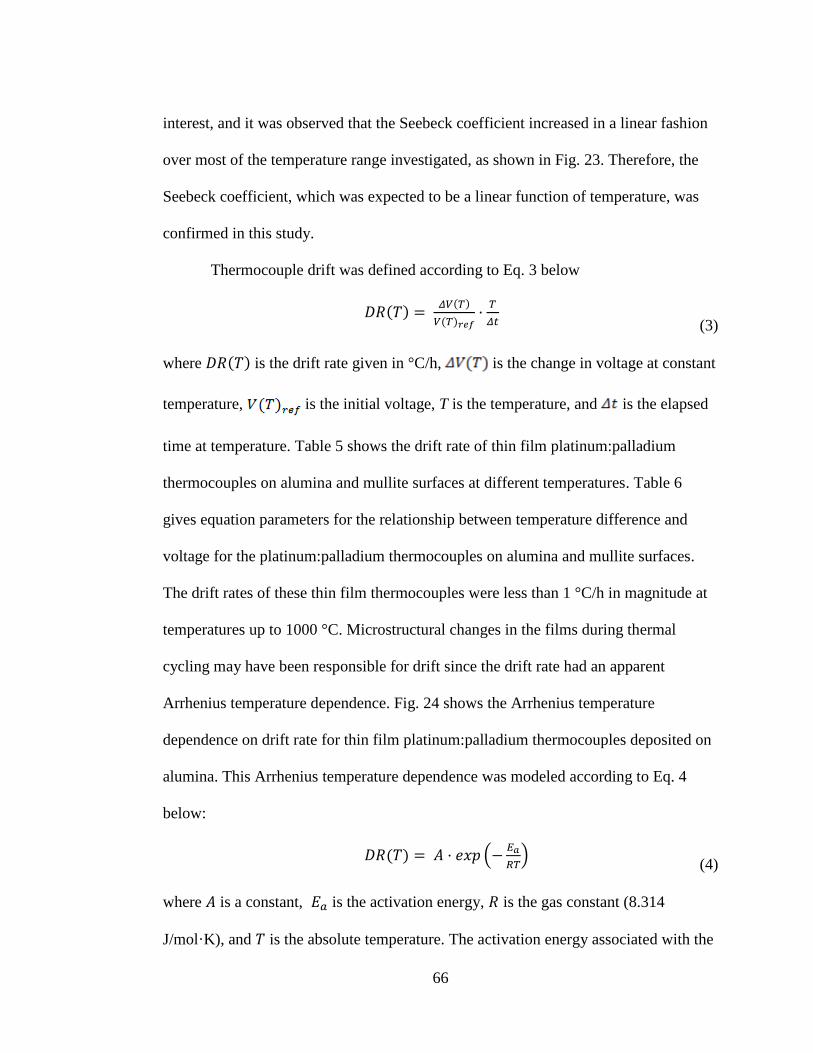
66
interest, and it was observed that the Seebeck coefficient increased in a linear fashion
over most of the temperature range investigated, as shown in Fig. 23. Therefore, the
Seebeck coefficient, which was expected to be a linear function of temperature, was
confirmed in this study.
Thermocouple drift was defined according to Eq. 3 below
(3)
where is the drift rate given in °C/h, is the change in voltage at constant
temperature, is the initial voltage, T is the temperature, and is the elapsed
time at temperature. Table 5 shows the drift rate of thin film platinum:palladium
thermocouples on alumina and mullite surfaces at different temperatures. Table 6
gives equation parameters for the relationship between temperature difference and
voltage for the platinum:palladium thermocouples on alumina and mullite surfaces.
The drift rates of these thin film thermocouples were less than 1 °C/h in magnitude at
temperatures up to 1000 °C. Microstructural changes in the films during thermal
cycling may have been responsible for drift since the drift rate had an apparent
Arrhenius temperature dependence. Fig. 24 shows the Arrhenius temperature
dependence on drift rate for thin film platinum:palladium thermocouples deposited on
alumina. This Arrhenius temperature dependence was modeled according to Eq. 4
below:
(4)
where is a constant, is the activation energy, is the gas constant (8.314
J/mol·K), and is the absolute temperature. The activation energy associated with the

67
Figure 23. Seebeck coefficient of platinum:palladium thermocouples on alumina and
mullite as a function of temperature and substrate.
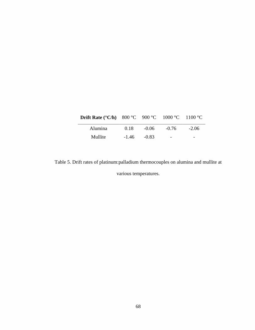
68
Drift Rate (°C/h) 800 °C 900 °C 1000 °C 1100 °C
Alumina 0.18 -0.06 -0.76 -2.06
Mullite -1.46 -0.83 - -
Table 5. Drift rates of platinum:palladium thermocouples on alumina and mullite at
various temperatures.
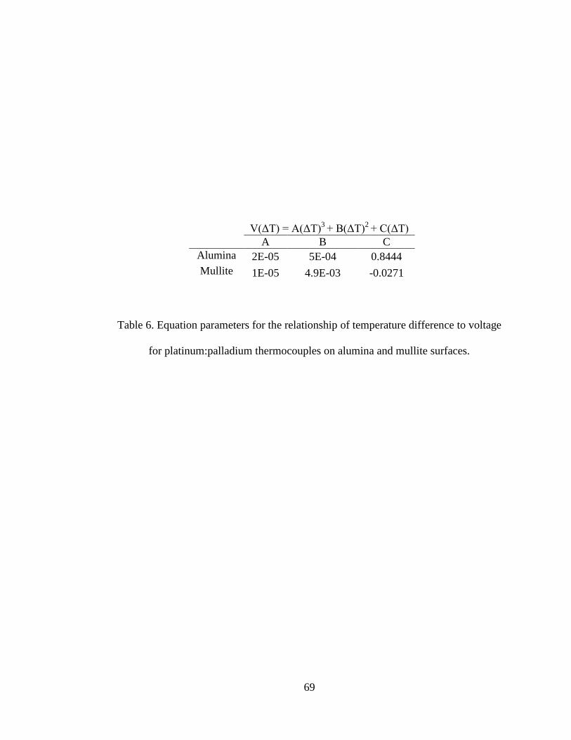
69
V(ΔT) = A(ΔT)3 + B(ΔT)
2 + C(ΔT)
A B C
Alumina 2E-05 5E-04 0.8444
Mullite 1E-05 4.9E-03 -0.0271
Table 6. Equation parameters for the relationship of temperature difference to voltage
for platinum:palladium thermocouples on alumina and mullite surfaces.
70
Figure 24. Drift rates of platinum:palladium thermocouples as a function of
temperature. Note the Arrhenius temperature dependance of the drift rates.
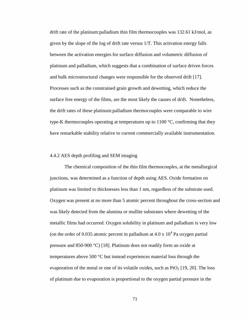
71
drift rate of the platinum:palladium thin film thermocouples was 132.61 kJ/mol, as
given by the slope of the log of drift rate versus 1/T. This activation energy falls
between the activation energies for surface diffusion and volumetric diffusion of
platinum and palladium, which suggests that a combination of surface driven forces
and bulk microstructural changes were responsible for the observed drift [17].
Processes such as the constrained grain growth and dewetting, which reduce the
surface free energy of the films, are the most likely the causes of drift. Nonetheless,
the drift rates of these platinum:palladium thermocouples were comparable to wire
type-K thermocouples operating at temperatures up to 1100 °C, confirming that they
have remarkable stability relative to current commercially available instrumentation.
4.4.2 AES depth profiling and SEM imaging
The chemical composition of the thin film thermocouples, at the metallurgical
junctions, was determined as a function of depth using AES. Oxide formation on
platinum was limited to thicknesses less than 1 nm, regardless of the substrate used.
Oxygen was present at no more than 5 atomic percent throughout the cross-section and
was likely detected from the alumina or mullite substrates where dewetting of the
metallic films had occurred. Oxygen solubility in platinum and palladium is very low
(on the order of 0.035 atomic percent in palladium at 4.0 x 10⁴ Pa oxygen partial
pressure and 850-900 °C) [18]. Platinum does not readily form an oxide at
temperatures above 500 °C but instead experiences material loss through the
evaporation of the metal or one of its volatile oxides, such as PtO2 [19, 20]. The loss
of platinum due to evaporation is proportional to the oxygen partial pressure in the
72
ambient, and is appreciably higher at atmospheric pressure between 1000 °C and 1100
°C, where PtO2 has a partial vapor pressure of 0.05 Pa [19]. Decomposition of the
volatile oxides at high temperature can result in the redeposition of the metal onto the
original surface, so the overall material loss is minimal compared to other noble
metals [19]. Therefore, any oxides that were present on the surface of the platinum
legs likely formed during cooling from elevated temperatures.
Oxide formation on palladium when deposited on alumina was limited to a
thickness of less than 1 nm, which was comparable to that of platinum films formed
on the same surface. Again, oxygen was still detected at greater film depths but was
likely due to the exposed substrate in areas where the metal film had dewetted.
Oxygen was detected at approximately 30 atomic percent to a depth of more than 25
nm for palladium deposited on mullite. However, the formation of condensed oxide
phases on the palladium is not likely; while material loss from evaporation of the
metal or of its volatile oxide, PdO, is much more likely [19]. At temperatures greater
than 850 °C, surface oxides on palladium typically decompose. The vapor pressure of
palladium metal at temperatures above 1000 °C exceeds that of PdO, especially at
atmospheric pressure, so material loss due to palladium metal evaporation likely
dominates the material loss mechanism [19, 20]. Therefore, it is likely that the high
atomic percentage of oxygen detected in the films is derived from the exposed mullite
surface in the vicinity of the dewetted palladium films. This dewetting phenomenon
was much more prevalent in the palladium films than platinum, as given by the atomic
percent oxygen detected for both thin films.
73
Considerable interdiffusion of platinum and palladium at the metallurgical
junctions of the thin film thermocouples was verified by AES depth profiling. Since a
complete solid solution of platinum and palladium will be formed at the junction, solid
solutions containing approximately 90/10 atomic percent platinum/palladium on
alumina and 78/22 atomic percent platinum/palladium on mullite were not surprising.
The platinum-palladium phase diagram provided further evidence of solid solution
formation in both metallurgical junctions [21]. Oxygen was detected at depths up to 15
nm at both metallurgical junctions; however, the detection of oxygen was most likely
from exposed substrate surfaces since it is not likely a metastable oxide film would
form at these depths in either platinum or palladium [19]. A larger atomic percentage
of oxygen in the metallurgical junction was detected on mullite because it experienced
a greater amount of dewetting after thermal cycling than the same junction formed on
alumina.
Dewetting in conjunction with faceting of both the platinum and palladium
films were observed in SEM, and these microstructural changes were apparent in the
thin film thermocouples deposited on both alumina and mullite. In all cases, dewetting
resulted in recrystallization and pore growth where the pore edges were faceted,
particularly at grain boundaries. Fig. 25 shows the microstructure of platinum and
palladium films on alumina and mullite. When deposited on alumina, the palladium
films contained larger pore sizes along with larger grains and more faceting, than
observed in the platinum films due to differences in the melting temperature of the two
metals. Furthermore, the surface recession rate of palladium is four orders of
magnitude higher than platinum due to surface energy considerations [19].

74
Figure 25. SEM micrographs using backscatter electron imaging (BSEI) of various
thin film thermocouple legs after high temperature cycling: platinum on alumina (a);
palladium on alumina (b); platinum on mullite (c); and palladium on mullite (d). Each
film exhibited dewetting with distinctly different microstructures due to long term
high temperature exposure.
75
When deposited on mullite, the platinum resembled a contiguous network of high
aspect ratio crystals and faceted islands with discrete pores. Palladium films deposited
on mullite appear to have similar dewetting characteristics relative to the palladium
film formed on alumina. Due to differences in surface roughness, the topography of
the palladium film appears different on mullite because it generally contains larger
pores and randomly dispersed smaller islands, which were not observed in the films
formed on alumina. The differences in the dewetting of these films results from
dissimilar surface energy and surface roughness of the substrates, where the rougher
surfaces tend to induce more residual stress on films, increasing their surface free
energy. Therefore, there is a greater driving force for dewetting of platinum and
palladium on mullite due to its relatively rougher surface. This is primarily responsible
for the different microstructures observed on alumina. All microstructures here
appeared to be similar to those formed via a vapor phase transport mechanism, in
which continuous and fully faceted networks of metal were formed throughout the
film due to the dewetting process [3]. Higher magnification revealed faceted striations
in the thermocouple legs, which are also suggestive of the vapor phase transport.
Various images of striations in the films are shown in Fig. 26a and Fig. 26b.
The microstructure of the metallurgical junctions showed no evidence of phase
separation since a complete solid solution was formed between platinum and
palladium after thermal cycling. The formation of faceted pores was evident in the
dewetted films; however, the extent to which this occurred in relation to platinum and
palladium was minimal. This was due to the increased thickness of the overlapping
platinum and palladium films at the junction relative to the individual legs. If more
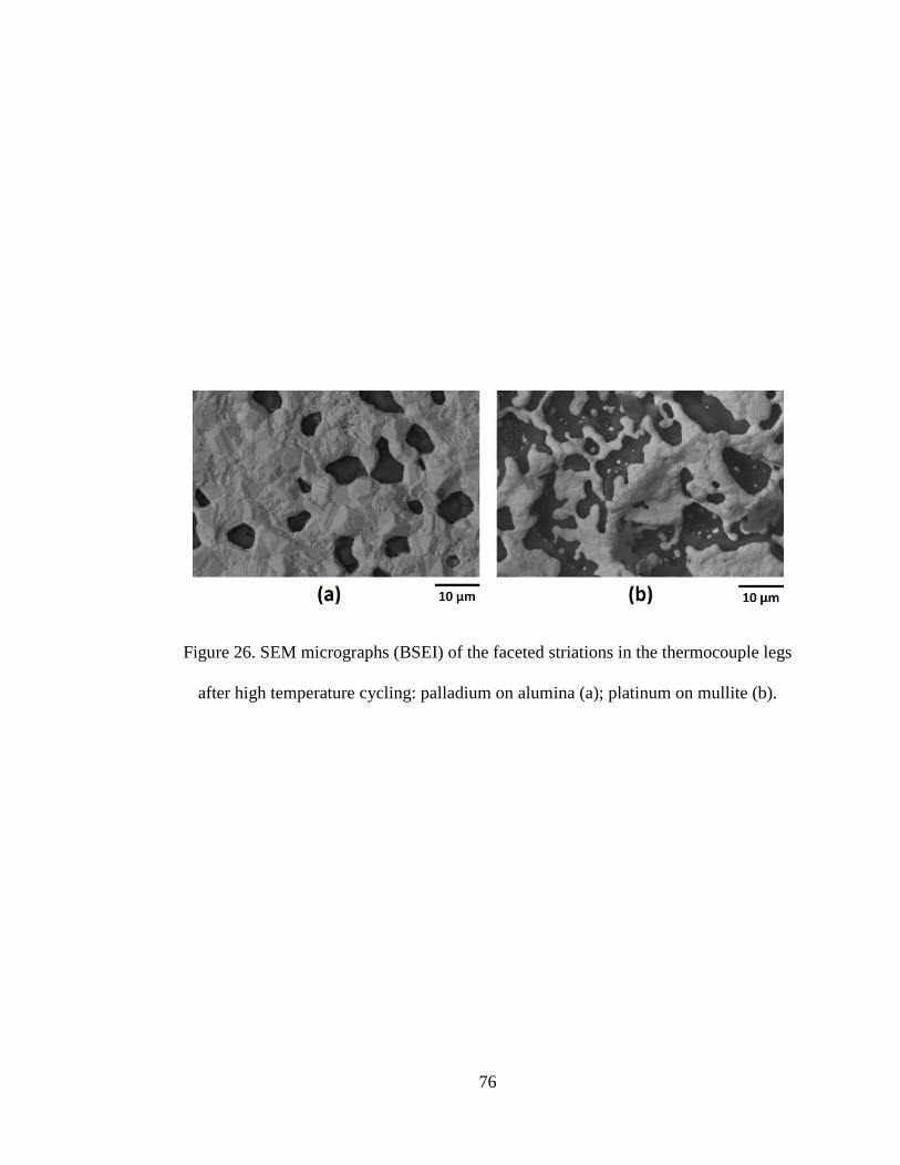
76
Figure 26. SEM micrographs (BSEI) of the faceted striations in the thermocouple legs
after high temperature cycling: palladium on alumina (a); platinum on mullite (b).
77
material is initially present, as in the case of the thermocouple junctions, the dewetting
process has the same microstructural effect. Similar to the platinum and palladium
films, faceted striations were observed at the metallurgical junction on both surfaces.
Delamination of the film was also observed at the metallurgical junction/palladium
interface where the junction had receded from the palladium film and was likely
driven by dewetting of the palladium film during thermal cycling. Delamination and
dewetting of these films would ultimately lead to device failure where, in the limit, the
platinum and palladium films would debond completely, most likely at the
junction/thermocouple leg interface.
4.5 Conclusion
Platinum:palladium thermocouples were developed to replace conventional
thin film thermocouples based on platinum-rhodium alloys. These alloys suffer from
high drift rates due to instability and degradation as a result of compositional changes
and selective oxidation processes during thermal cycling. The platinum:palladium thin
film thermocouples did not show the detrimental effects of selective oxidation and its
adverse effect on the chemical stability of the metallurgical junction. Therefore, the
drift rates observed for these thermocouples were comparable to conventional type-K
wire thermocouples during thermal cycling. Thicker (thin film) thermocouples would
prolong the stability of these sensors by inhibiting dewetting and unfavorable
microstructural changes in the films during thermal cycling. The thermoelectric
performance of these thermocouples at high temperature makes them promising
candidates for implementation in the harsh environments of gas turbine engines, and

78
given their stability, long term sensing at temperatures in excess of 1100 °C will be
possible.

79
List of References
[1] J. D. Wrbanek, G. C. Fralick, and D. Zhu, Thin Solid Films 520 (2012) 5801.
[2] O. J. Gregory, M. Amani, I. M. Tougas, and A. J. Drehman, J. Am. Ceram. Soc. 95
(2012) 705.
[3] G. E. Aniolek and O. J. Gregory, Surf. Coat. Tech. 68-69 (1994) 70.
[4] J. F. Lei and H. A. Will, Sens. Actuators, A 65 (1998) 187.
[5] L. C. Martin and R. Holanda, NASA TM-106714, (1994).
[6] H. Choi and X. Li, Sens. Actuators, A 136 (2007) 118.
[7] K. G. Kreider, J. Vac. Sci. Technol., A 11 (1993) 1401.
[8] D. Wang and P. Schaaf, J. Mater. Sci.: Mater. Electron. 22 (2011) 1067.
[9] K. D. Hill, Metrologia 39 (2002) 51.
[10] M. G. Ahmed and K. Ali, J. Metrology Soc. India 23 (2008) 225.
[11] G. W. Burns, D. C. Ripple, and M. Battuello, Metrologia 35 (1998) 761.
[12] Y. A. Abdelaziz, F. M. Megahed, and M. M. Halawa, Measurement 35 (2004)
413.
[13] N. P. Moiseeva, Meas. Tech. 47 (2004) 915.
[14] K. G. Kreider and G. Gillen, Thin Solid Films, 376 (2000) 32.
[15] K. G. Kreider and F. DiMeo, Sens. Actuators, A 69 (1998) 46.
[16] Revised Thermocouple Reference Tables: Type S, Omega Engineering,
Stamford, CT. [http://www.omega.com/temperature/Z/pdf/z208-209.pdf]
[17] I. Beszeda, E. G. Gontier-Moya, and D. L. Beke, Surf. Sci., 547 (2003) 229.
[18] J. Gegner, G. Hörz, and R. Kirchheim, J. Mater. Sci., 44 (2009) 2198.
[19] H. Jehn, J. Less-Common Met., 100 (1984) 321.
80
[20] J. C. Chaston, Platinum Metals. Rev., 19 (1975) 135.
[21] S. R. Bharadwaj, A. S. Kerkar, S. N. Tripathi, and S. R. Dharwadkar, J. Less-
Common Met., 169 (1991) 167.

81
CHAPTER 5
FUTURE WORK
5.1 Thin Film Thermocouples
Gas turbine engines consume immense amounts of energy from combusting
fuels in order to produce thrust or energy for the generation of electricity. In order to
meet increasing energy regulations, engine companies are putting tireless effort into
improving the efficiency of gas turbine engines. One fundamental way in which this is
being progressively achieved is through increasing the operating temperature of the
hot section inside the engine. With higher temperatures comes increased efficiency
which is defined simply by Carnot’s theorem given as η = 1 – TC/TH where TC is the
cold reservoir temperature and TH is the hot reservoir temperature. Therefore, by
increasing the hot section temperature relative to the surroundings, the thermodynamic
efficiency of these engines will increase.
As a result, gas turbine engine manufacturers are met with new challenges to
design materials and sensors which can handle the increasingly harsh high temperature
environment inside the engine hot section of these more efficient engines.
Conventional superalloy materials cannot withstand the 1500°C or higher hot section
temperatures in these new engines, therefore ceramic matrix composite (CMC)
materials are being developed and employed in these next generation engines. These
materials can withstand the increased operating temperatures with superior
thermomechanical properties and lower mass relative to superalloy materials. Silicon
82
carbide based CMCs are currently being developed for implementation inside engine
hot sections as turbine blades and components of the combustion chamber. Other
issues also arise with the implementation of these CMC materials, such as the need for
alternative thermal barrier coatings (TBC) on the surface of parts. These TBCs must
have similar thermal expansion coefficients to the CMC so that they exhibit great
adhesion during thermal cycling. Additionally, there is a need to develop new sensors
or modify existing sensors so they are with the TBCs implemented on CMC
components, and they must be able to withstand the increased hot section
temperatures. Research has already begun to instrument CMCs for gas turbine engine
applications.1 The CMC, TBC, and thermocouples must be integrated in the following
way:
The TBC must planarize the CMC material prior to the implementation of a
thermocouple while also providing environmental protection.
The TBC must form a dielectric barrier between the CMC material and the
thermocouple.
The thermocouple materials chosen should have similar thermal expansion
coefficients to the TBC material and be able to withstand the extreme
temperatures over long periods and many cycles.
Based on the work in this thesis, the most promising thermocouple materials for the
instrumentation of CMC materials are In2O3-ITO and Pt-Pd based. By sticking to the
above guidelines carefully and designing experiments accordingly, the implementation
of sensors inside next generation CMC-based gas turbine engines will be achievable.

83
Thermoelectrics based on p-type and n-type films in the Cu-In-O system are
currently being fabricated as the continuation of the research presented in chapter 3 of
this thesis. Targets have been fabricated using powder processing techniques of the
best performing p-type (22 at% In) and n-type (57 at% In) materials from the Cu-In-O
system combinatorial library. It is anticipated that the combination of the p-type and n-
type Cu-In-O materials will enable the fabrication of a p-n junction for thermoelectric
applications comprised of materials from the same system. Additionally, another
compound in the Cu-In-O system (22 at% In) was found to exhibit a totally
amorphous structure after the film was annealed in nitrogen at 400°C for 5h followed
by annealing at 1000°C for 2h in air. Essentially, at this ratio of CuO to In2O3, the
material maintains its amorphous structure to high temperature, even in the presence
of oxygen.
84
List of References
1Ceramic thin film thermocouples for SiC-based ceramic matrix composites, J. D.
Wrbanek, G. C. Fralick, and D. Zhu, Thin Solid Films, 2012

85
BIBLIOGRAPHY
Abdelaziz, Y. A., Megahed, F. M., and Halawa, M. M., “Stability and calibration of
platinum-palladium thermocouples following heat treatment,” Measurement, 2004, pp.
413.
Ahmed, M. G. and Ali, K., “Investigating Pt-Pd Thermocouples in the Temperature
Range from 800°C to 1500°C at the National Institute of Standards NIS-Egypt,”
Journal of Metrology Society of India, 2008, pp. 225.
Amani, M., Tougas, I. M., Gregory, O. J., and Fralick, G. C., “Thermoelectric
Properties of ZnxInyOx+1.5y Films,” Journal of Electronic Materials, 2013, pp. 114.
Aniolek, G. E. and Gregory, O. J., “Thin film thermocouples for advanced ceramic gas
turbine engines,” Surface and Coatings Technology, 1994, pp. 70.
Aperathitis, E., Bender, M., Cimalla, V., Ecke, G., and Modreanu, M., “Properties of
rf-sputtered indium-tin-oxynitride thin films,” Journal of Applied Physics, 2003.
Aperathitis, E., Modreanu, M., Bender, M., Cimalla, V., Ecke, G., Androulidaki, M.,
and Pelekanos, N., “Optical characterization of indium-tin-oxynitride fabricated by
RF-sputtering,” Thin Solid Films, 2004, pp. 101.
Bentley, R. E., “Handbook of Temperature Measurement Vol. 3: Theory and Practice
of Thermoelectric Thermometry”, Springer, 1998.
Bérardan, D., Guilmeau, E., Maignan, M., and Raveau, B., “Enhancement of the
thermoelectric performances of In2O3 by the coupled substitution of M2+
/Sn4+
for
In3+,” Journal of Applied Physics, 2008, pp. 064918.
Beszeda, I., Gontier-Moya, E. G., and Beke, D. L., “Investigation of mass transfer
surface self-diffusion on palladium,” Surface Science, 2003, pp. 229.
Bharadwaj, S. R., Kerkar, A. S., Tripathi, S. N., and Dharwadkar, S. R., “The
palladium-platinum phase diagram,” Journal of the Less Common Metals, 1991, pp.
167.
Bosacka, M., Filipek, E., Šulcova, P., Dohnalová, Ž., and Paczesna, A., “Phase
equilibria in the solid state and colour properties of the CuO-In2O3 system,” Journal of
Thermal Analysis and Calorimetry, 2012, pp. 605.
Burns, G. W., Ripple, D. C., and Battuello, M., “Platinum versus palladium
thermocouples – an emf-temperature reference function for the range 0C to 1500C,”
Metrologia, 1998, pp. 761.

86
Chadwick, A. V., Blacklocks, A. N., Rougier, A., and Yaicle, C., “A Structural Study
of Delafossite-type CuInO2 Thin Films,” Journal of Physics: Conference Series, 2010,
pp. 012045.
Chaston, J. C., “The Oxidation of the Platinum Metals – A Descriptive Survey of the
Reactions Involved,” Platinum Metals Review, 1975, pp. 135.
Chen, X., Gregory, O. J., and Amani, M., “Thin-Film Thermocouples Based on the
System In2O3-SnO2,” Journal of the American Ceramic Society, 2011, pp. 854.
Choi, H. And Li, X., “Fabrication and application of micro thin film thermocouples
for transient temperature measurement in nanosecond pulsed laser micromachining of
nickel,” Sensors and Actuators A, 2007, pp. 118.
Ellmer, K. and Mientus, R., “Carrier transport in polycrystalline ITO and ZnO:Al II:
The influence of grain barriers and boundaries,” Thin Solid Films, 2008, pp. 5829.
Garino, T. J. and Bowen, H. K., “Kinetics of Constrained-Film Sintering,” Journal of
the American Ceramic Society, 1990, pp. 251.
Gegner, J., Hörz, G., and Kirchheim, R., “Diffusivity and solubility of oxygen in solid
palladium,” Journal of Materials Science, 2009, pp. 2198.
Granqvist, C. G., “Transparent conductors as solar energy materials: A panoramic
review,” Solar Energy Materials and Solar Cells, 2007, pp. 1529.
Gregory, O. J. and Amani, M., “Thermoelectric Properties of ZnxInyOx+1.5y Films,”
Journal of the Electrochemical Society, 2011, pp. J15.
Gregory, O. J., Amani, M., Tougas, I. M., and Drehman, A. J., “Stability and
Microstructure of Indium Tin Oxynitride Thin Films,” Journal of the American
Ceramic Society, 2012, pp. 705.
Gregory, O. J., Lee, S. B., Flagan, R. C., “Reaction Sintering of Submicrometer
Silicon Powder,” Journal of the American Ceramic Society, 1987, pp. C52.
Gregory, O. J., Luo, Q., and Crisman, E. E., “High Temperature Stability of Indium
Tin Oxide Thin Films,” Thin Solid Films, 2002, pp. 286.
Gregory, O. J. and You, T., “Piezoresistive Properties of ITO Strain Sensors Prepared
with Controlled Nanoporosity,” Journal of the Electrochemical Society, 2004, pp.
H198.
Harvey, S. P., Mason, T.O., Gassenbauer, Y., Schafranek, R., and Klein, A., “Surface
versus bulk electronic/defect structures of transparent conducting oxides: I. Indium
oxide and ITO,” Journal of Physics D: Applied Physics, 2006, pp. 3959.
87
Hill, K. D., “An investigation of palladium oxidation in the platinum-palladium
thermocouple system,” Metrologia, 2002, pp. 51.
Hopper, E. M., Zhu, Q., Song, J-H., Peng, H., Freeman, A. J., and Mason, T. O.,
“Electronic and thermoelectric analysis of phases in the In2O3(ZnO)k system,” Journal
of Applied Physics, 2011, pp. 013713.
Jehn, H., “High Temperature Behavior of Platinum Group Metals in Oxidizing
Atmospheres, Journal of the Less Common Metals, 1984, pp. 321.
Jonker, G., “The application of combined conductivity and Seebeck-effect plots for
the analysis of semiconducting properties,” Philips Journal of Research, 1968, pp.
131.
Kaga, H., Asahi, R., and Tani, T., “Thermoelectric Properties of Doped (ZnO)mIn2O3,”
Japanese Journal of Applied Physics, 2004, pp. 3540.
Kawazoe, H., Yasukawa, M., Hyodo, H., Kurita, M., Yanagi, H., and Hosono, H., “P-
type electrical conduction in transparent thin films of CuAlO2,” Nature, 1997, pp. 939.
Kim, K. C., Lee, J. H., Kim, J. J., Ikegami, T., “Rapid rate sintering of nanocrystalline
indium tin oxide ceramics: particle size effect,” Materials Letters, 2002, pp. 114.
Kreider, K. G., “Sputtered high temperature thin film thermocouples,” Journal of
Vacuum Science Technology, 1993, pp. 1401.
Kreider, K. G. and DiMeo, F., “Platinum-palladium thin-film thermocouples for
temperature measurements on silicon wafers,” Sensors and Actuators, A, 1998, pp. 46.
Kreider, K. G. and Gillen, G., “High temperature materials for thin-film
thermocouples on silicon wafers,” Thin Solid Films, 2000, pp. 32.
Lee, J-C., Heo, Y-W., Lee, J-H., and Kim, J-J., “Growth of CuInO2 thin film using
highly dense Cu2O-In2O3 composite targets,” Thin Solid Films, 2009, pp. 1234.
Lei, J. F. and Will, H. A., “Thin-Film Thermocouples and Strain-Gauge Technologies
for Engine Applications,” Sensors and Actuators A, 1998, pp. 187.
Liu, L., Bai, K., Gong, H., and Wu, P., “First-Principles Study of Bipolar Dopability
in the CuInO2 Transparent Semiconductor,” Chemistry of Materials, 2005, pp. 5529.
Martin, L. C. and Holanda, R., “Applications of Thin Film Thermocouples for Surface
Temperature Measurement,” NASA TM-106714, 1994.
88
Medvedovski, E., Szepesi, C. J., Yankov, O., Lippens, P., “Indium tin oxide nanosized
transparent conductive thin films obtained by sputtering from large size planar and
rotary targets,” Ceramic Transactions, 2010, pp. 125.
Moiseeva, N. P., “The prospect for developing standard thermocouples of pure
metals,” Measurement Science and Technology, 2004, pp. 915.
Nomura, K., Ohta, H., Takagi, A., Kamiya, T., Hirano, M., and Hosono, H.,
Amorphous Oxide Semiconductors for High-Performance Flexible Thin-Film
Transistors,” Nature, 2004, pp. 4308.
Omega Engineering, “Revised Thermocouple Reference Tables: Type S,” Stamford,
CT, [http://www.omega.com/temperature/Z/pdf/z208-209.pdf].
Shimode, M., Sasaki, M., Mukaida, K., “Synthesis of the Delafossite-Type CuInO2,”
Journal of Solid State Chemistry, 2000, pp. 16.
Varela, J. A., Whittemore, O. J., Longo, E., “Pore size evolution during sintering of
ceramic oxides,” Ceramics International, 1990, pp. 177.
Wang, D. and Schaaf, P., “Two-dimensional nanoparticle arrays formed by dewetting
of thin gold films deposited on pre-patterned substrates,” Journal of Materials
Science: Materials in Electronics, 2011, pp. 1067.
Wrbanek, J. D., Fralick, G. C., and Zhu, D., “Ceramic thin film thermocouples for
SiC-based ceramic matrix composites,” Thin Solid Films, 2012, pp. 5801.
Yanagi, H., Hase, T., Ibuki, S., Ueda, K., and Hosono, H., “Bipolarity in electrical
conduction of transparent oxide semiconductor CuInO2 with delafossite structure,”
Applied Physics Letters, 2001, pp. 1583.
Yin, M., Wu, C-K., Lou, Y., Burda, C., Koberstein, J. T., Zhu, Y., and O’Brien, S.,
“Copper Oxide Nanocrystals,” Journal of the American Chemical Society, 2005, pp.
9506.