Thick film multilayer microwave circuits for wireless applications
34
Thick-Film Multilayer Microwave Circuits for Wireless Applications By Kavindra krishna Research Scholar AMU Department of Electronics Engineering AMU 1
-
Upload
kavindrakrishna -
Category
Engineering
-
view
24 -
download
3
Transcript of Thick film multilayer microwave circuits for wireless applications

Thick-Film Multilayer Microwave Circuits for Wireless Applications
By
Kavindra krishna
Research Scholar
AMU
Department of Electronics Engineering AMU 1

CONTENTS
Introduction
Thick-film technology
Significance of line losses
Single layer microwave circuits
Multilayer microwave circuits
Summary
2

INTRODUCTON
3

Typical frequencies for wireless application :
Current mobile : 0.9GHz - 2GHz
3G systems : 2.5GHz
Bluetooth : 2.5GHz
GPS : 12.6GHz
LMDS : 24GHz and 40GHz
Automotive : 77GHz
4

LMDS (Local Multi Point Distribution Services)
5

Driving forces created by the wireless market:
lower cost
higher performance
greater functionality
increased packing density
6

Microstrip: basic microwave interconnection
structure
It provides one free surface on which solid state device can be placed.
7

Summary of key material requirements at RF: Conductors: - low bulk resistivity
- good surface finish (low surface roughness)
- high line/space resolution
- good temperature stability
Dielectrics: - low loss tangent (<10-2)
- good surface finish
- precisely defined r (stable with frequency)
- isotropic r
- consistent substrate thickness
- low Tf (< 50 ppm/oC)
8

THICK-FILM TECHNOLOGY
9

Thick-Film Technology
Advantages:
Low Cost
Feasibility for mass production
Adequate quality at microwave frequencies
Potential for multi-layer circuit structures
Difficulty:
Fabrication of fine line and gaps: limited
quality by direct screen printing
10

Standard range of materials is used:
CONDUCTORS: - gold
- silver
- copper
DIELECTRICS: - ceramic (alumina)
- green tape (LTCC)
- thick-film pastes
- laminates
Plus photoimageable conductors and dielectrics.
11

Fine lines < 25 micron with 1 micron
precision
High density, 4 micron thick conductor
High conductivity - 95% of bulk
96% Al
50m lines
Photodefined conductors 12

Losses in Thick-Film Technology
• Skin effect: at RF and microwave frequencies current tends to flow only in the surface of a conductor.
• Skin depth (): depth of penetration at which the magnitude of the current has decreased to 1/e of the surface value.
• Effect due to loss tangent on line : - this effect is shown in figure [1] on next slide.
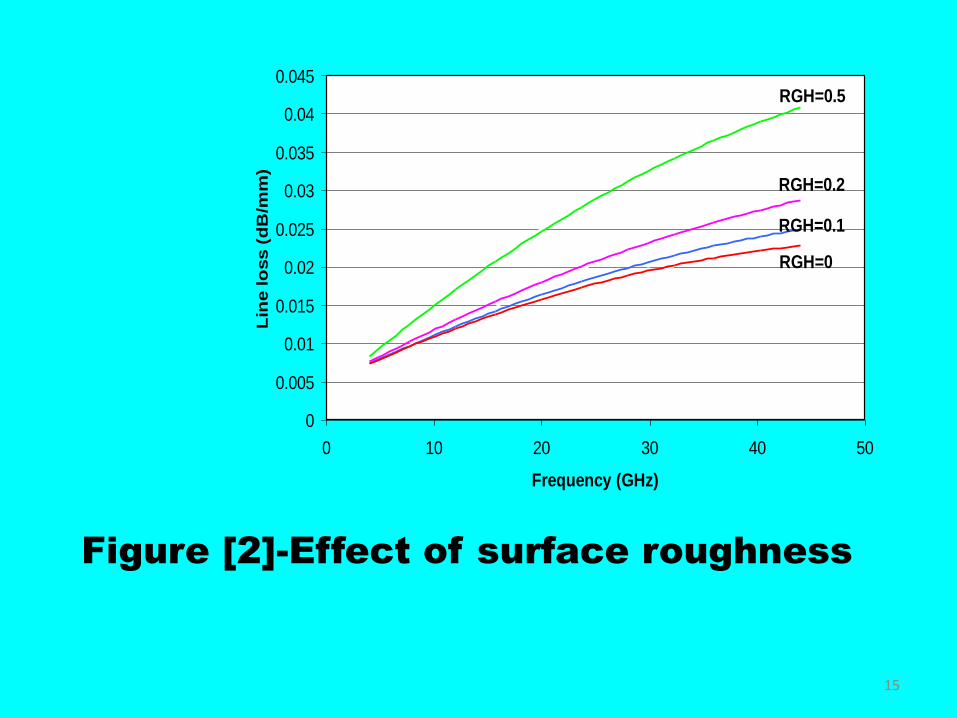
• Effect due to surface roughness:-the roughness on surface creates a loss,shown in figure [2]
f
1
13

Figure [1]-Effect of loss tangent on line
14
0
0.005
0.01
0.015
0.02
0.025
0.03
0.035
0.04
0.045
0 10 20 30 40 50
Frequency (GHz)
Lin
e lo
ss (
dB
/mm
)
RGH=0.5
RGH=0.2
RGH=0.1
RGH=0
Figure [2]-Effect of surface roughness
15
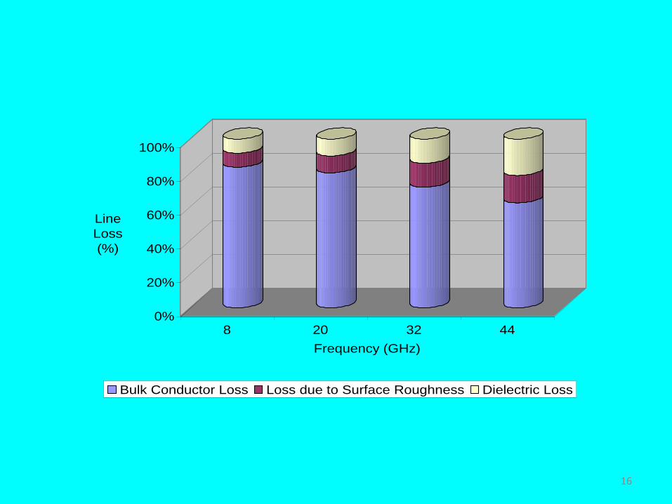
0%
20%
40%
60%
80%
100%
Line
Loss
(%)
8 20 32 44
Frequency (GHz)
Bulk Conductor Loss Loss due to Surface Roughness Dielectric Loss
16

0%
10%
20%
30%
40%
50%
60%
70%
80%
90%
100%
Line
Loss
(%)
Al LTCC
Different Material (evaluated at 2GHz)
Bulk Conductor Loss Loss due to Surface Roughness Dielectric Loss
17

LTCC TECHNOLOGY
• LTCC technology is a well-established technology
• Reliability established in the automotive market
• Advantages for high frequency applications:
• parallel processing ( reduced cost)
• precisely defined parameters
• high performance conductors
• potential for multi-layer structures
• high interconnect density
18

LTCC TECHNOLOGY
For Microwave applications:-
• LTCC can meet the physical and electrical
performance demanded at frequencies above
1GHz.
• Increases in material and circuit production are
reflected in lower costs: LTCC is now comparable
to other technologies.
• Significant space savings when compared to other
technologies.
19

SINGLE-LAYER
MICROWAVE CIRCUITS
20

Single-layer microstrip circuits:
all conductors in a single layer
coupling between conductors achieved
through edge or end proximity (across
narrow gaps)
Problem:
difficult to fabricate (cheaply in production)
fine gaps, possibly 10m
21

End-coupled
filter
Directional
coupler
Examples of single-layer microstrip circuits
22

MULTI-LAYER MICROWAVE CIRCUITS
23

Multilayer Microwave Circuits:
conductors stacked on different layers
conductors separated by dielectric layers
allows for (strong) broadside coupling
eliminated need for fine gaps
registration between layers not as difficult to
achieve as narrow gaps
technique well-suited to thick-film print technology
also suitable for LTCC technology
24

3 Isolated port
Direct port 4
Ground plane
H
h1
εr W1
W2
εr1
1
2 Coupled port
l
S
Main substrate
Thick-film dielectric layer
Input port
Multilayer
configuration
25

Thick-film technology is particularly suitable for the
implementation of multilayer circuits:
higher packing density
integration of antenna
close coupling between conductors
Circuit examples:
DC block
Directional coupler
26

Directional Coupler
• Directional coupler under multi -
Layer concept and single layer concept.
27

Measured result of 2dB directional coupler under multi layer concept
28

Microstrip DC Block
29

Multi layer DC Block
30

0
0.4
0.8
1.2
1.6
2
1 2 3 4 5 6 7 8 9 10 11 12
Frequency (GHz)
Inse
rtio
n L
oss (
dB
)
Measured performance of multilayer DC block
31
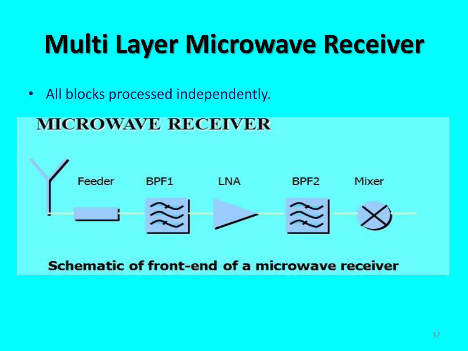
Multi Layer Microwave Receiver
• All blocks processed independently.
32

Comparison
• The variation in noise figure is reduced as compare to single layer fabrication.
33

SUMMARY
Thick-film technology provides a viable fabrication
process for wireless circuits at microwave frequencies
Multilayer microwave circuits can offer enhanced
performance for coupled-line circuits
Photoimageable thick-film materials extend the usable
frequency range to mm-wavelengths
34