Managing Talent in a VUCA World - SEMI...Exciting VUCA Times Ahead Semiconductors and Displays have...
20
Managing Talent in a VUCA World James Robson Corporate Vice President Applied Materials Europe
Transcript of Managing Talent in a VUCA World - SEMI...Exciting VUCA Times Ahead Semiconductors and Displays have...
Managing Talent in a VUCA World
James Robson
Corporate Vice President
Applied Materials Europe

Agenda
▪ Applied Materials Overview
▪ Today‘s VUCA World
▪ Talent Management
‒ Hiring
‒ Training & Developing
‒ Retaining
▪ Summary
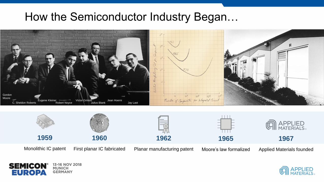
How the Semiconductor Industry Began…
Gordon
Moore
C. Sheldon RobertsEugene Kleiner
Robert NoyceVictor Grinish
Julius BlankJean Hoerni
Jay Last
1959
Monolithic IC patent
1960
First planar IC fabricated
1962
Planar manufacturing patent
1965
Moore’s law formalized
1967
Applied Materials founded
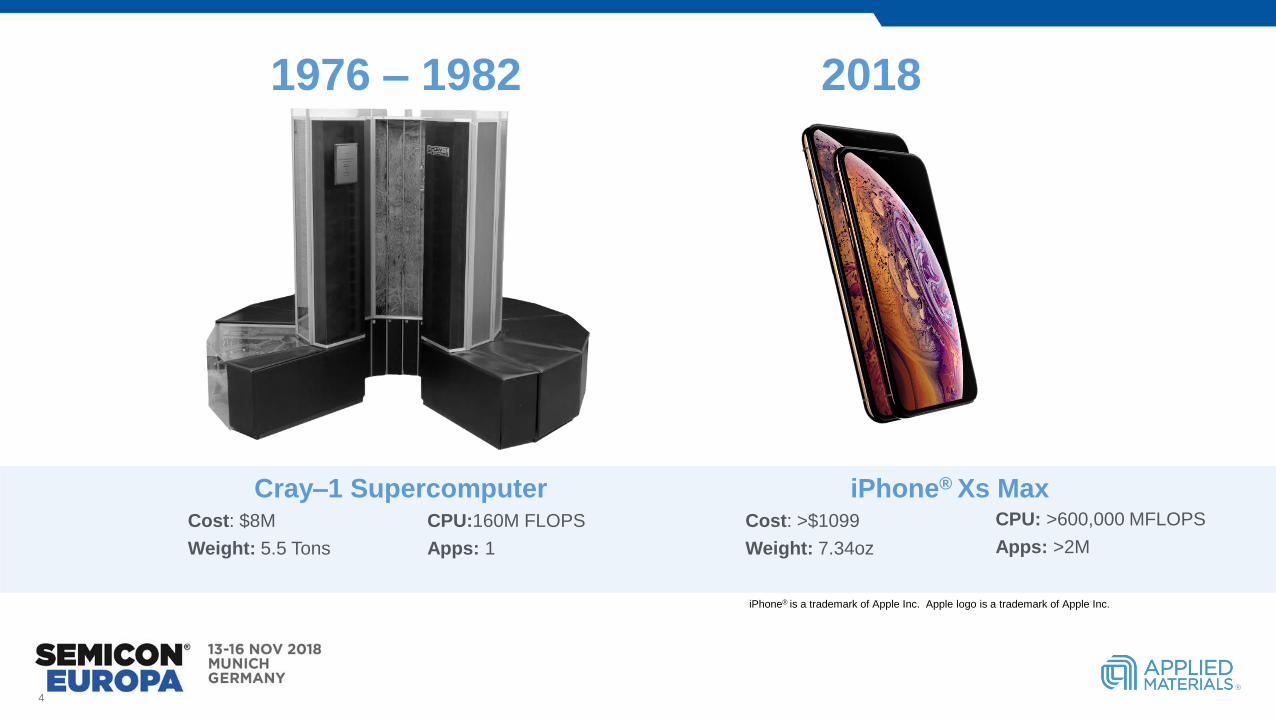
1976 – 1982
4
iPhone® is a trademark of Apple Inc. Apple logo is a trademark of Apple Inc.
Cray–1 SupercomputerCost: $8M CPU:160M FLOPS
Weight: 5.5 Tons Apps: 1
iPhone® Xs MaxCost: >$1099
Weight: 7.34oz
2018
CPU: >600,000 MFLOPS
Apps: >2M
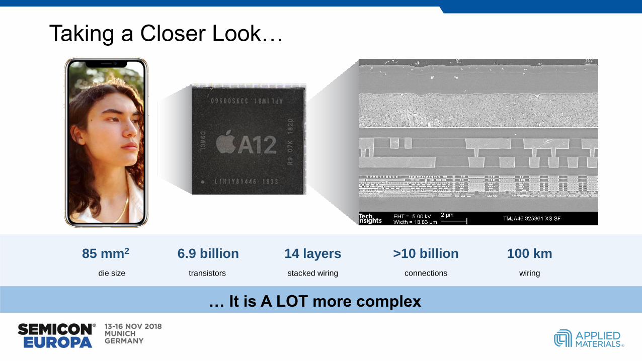
Taking a Closer Look…
… It is A LOT more complex
6.9 billion
transistors
14 layers
stacked wiring
>10 billion
connections
100 km
wiring
85 mm2
die size

6
Global leader in
Creating, modifying and analyzing
materials at an atomic level on an
industrial scale
MARKETS WE SERVEWHAT WE DO
Semiconductor
Display
materials engineering
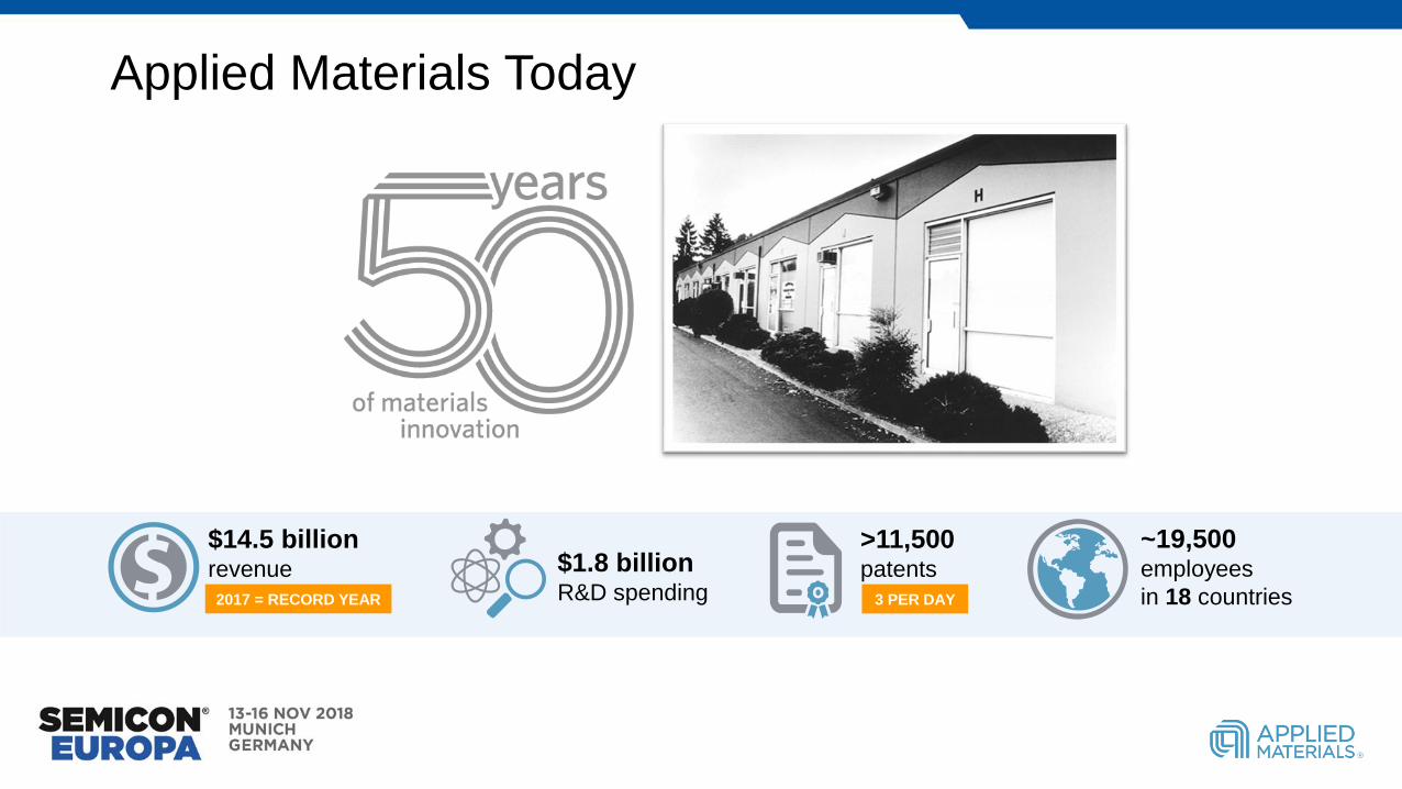
$1.8 billionR&D spending
~19,500 employees
in 18 countries
$14.5 billionrevenue
2017 = RECORD YEAR
>11,500patents
3 PER DAY
Applied Materials Today

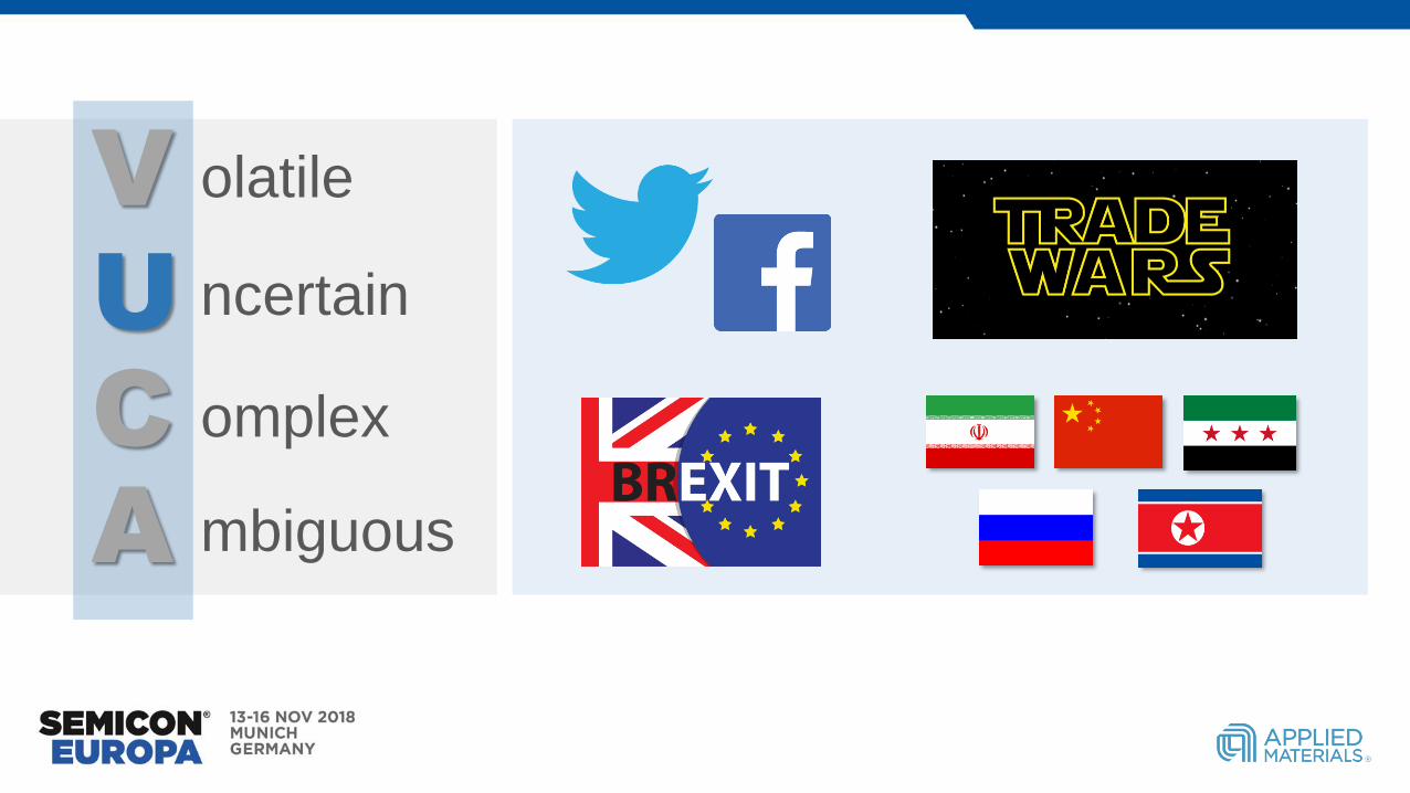
V
UCA
olatile
ncertain
omplex
mbiguous
V
UCA
olatile
ncertain
omplex
mbiguous
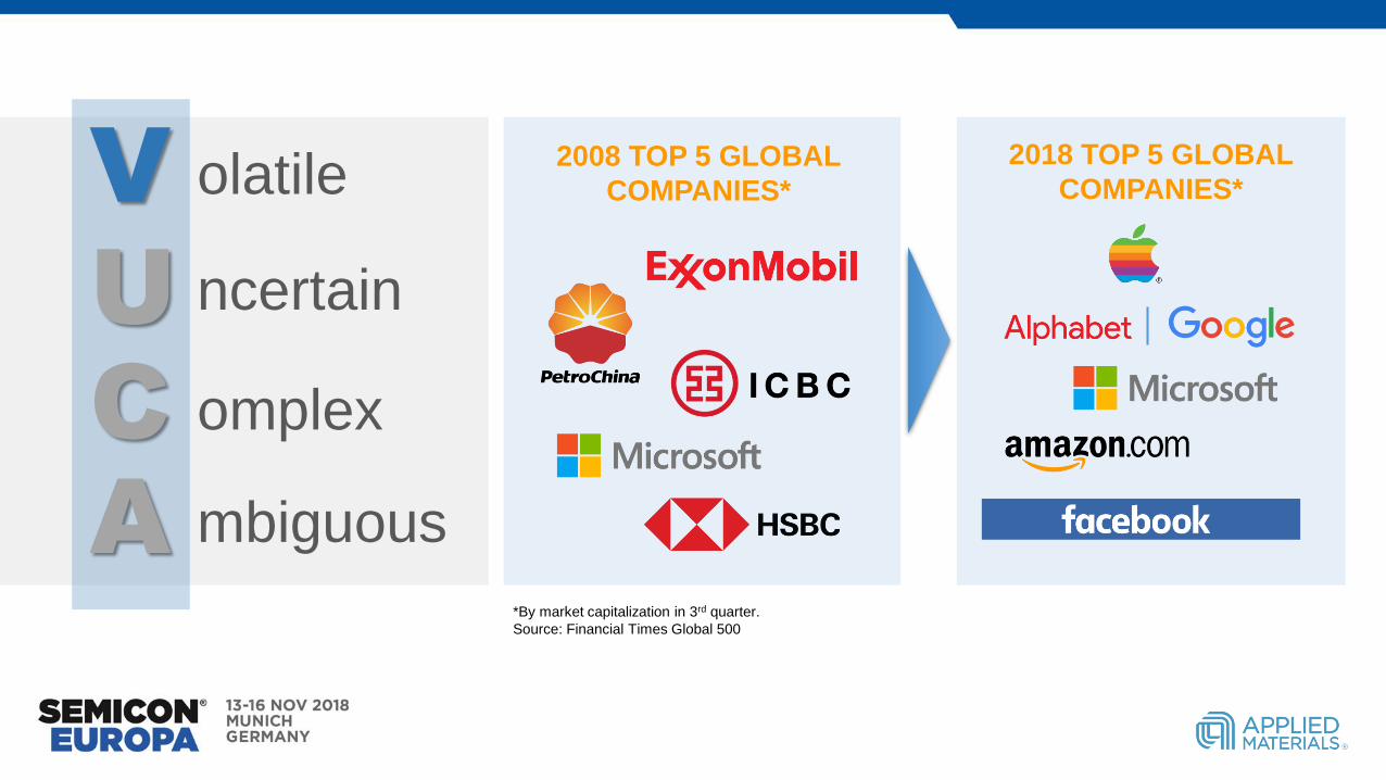
2018 TOP 5 GLOBAL
COMPANIES* 2008 TOP 5 GLOBAL
COMPANIES*
*By market capitalization in 3rd quarter.
Source: Financial Times Global 500
V
UCA
olatile
ncertain
omplex
mbiguous
V
UCA
olatile
ncertain
omplex
mbiguous
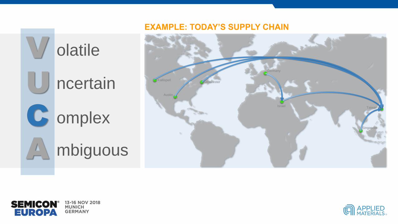
EXAMPLE: TODAY’S SUPPLY CHAIN
Germany
Israel Taiwan
Austin
KallispellGloucester
Singapore
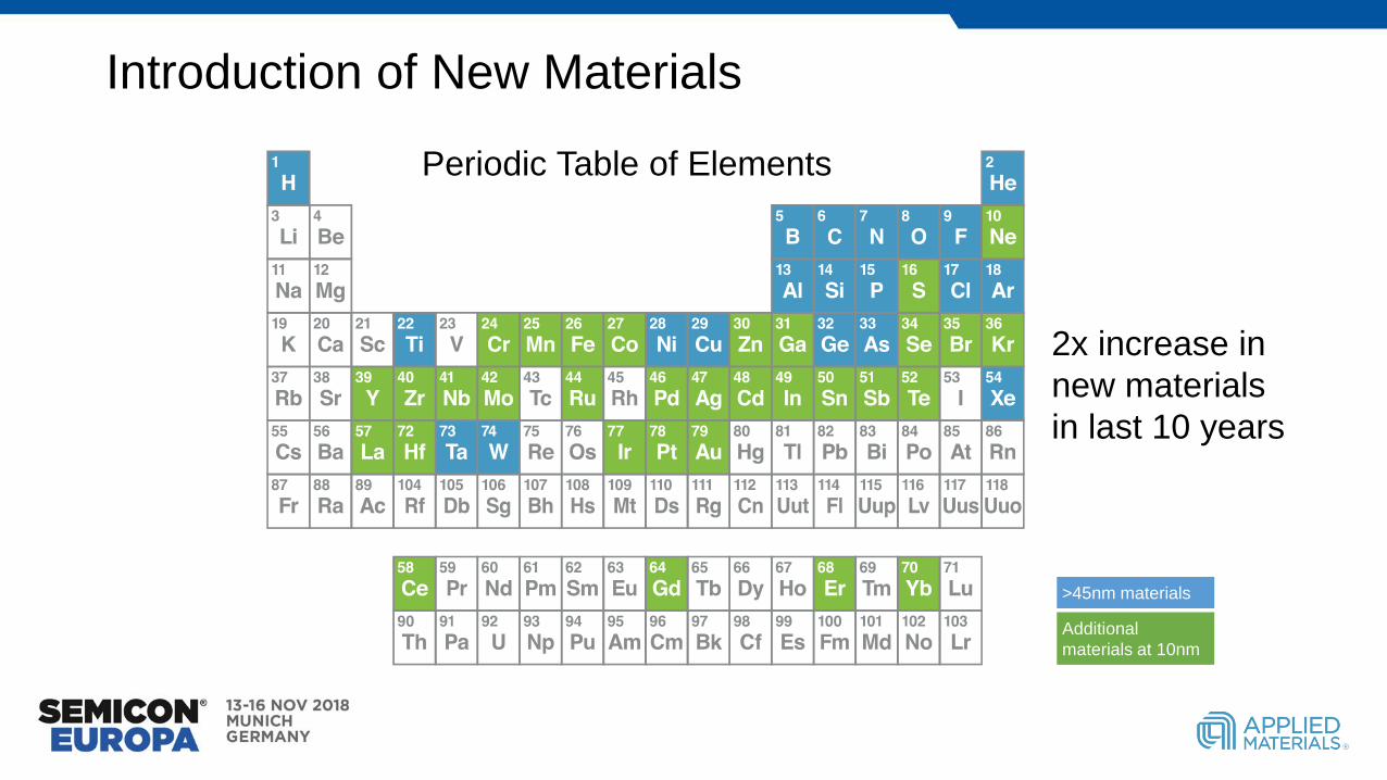
2x increase in
new materials
in last 10 years
Introduction of New Materials
>45nm materials
Additional
materials at 10nm
Periodic Table of Elements
V
UCA
olatile
ncertain
omplex
mbiguous
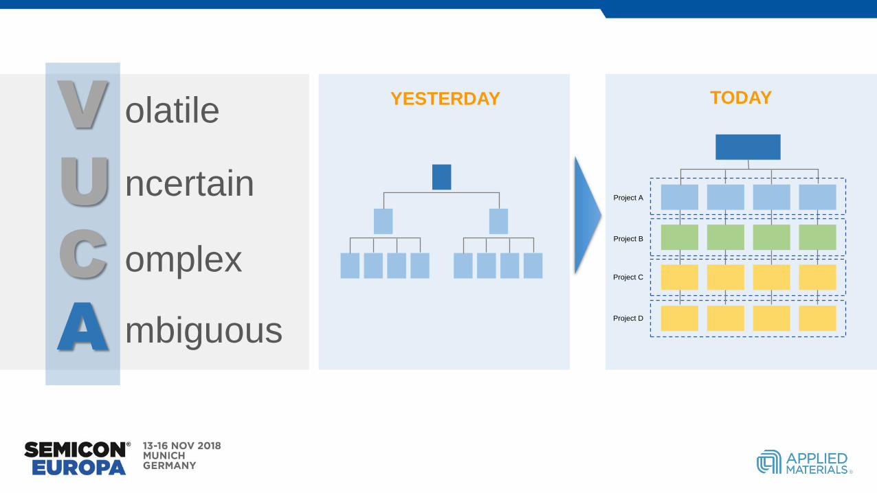
TODAYYESTERDAY
Project B
Project C
Project D
Project A
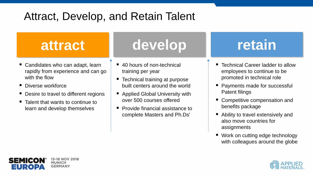
Attract, Develop, and Retain Talent
attract develop retain
▪ Candidates who can adapt, learn
rapidly from experience and can go
with the flow
▪ Diverse workforce
▪ Desire to travel to different regions
▪ Talent that wants to continue to
learn and develop themselves
▪ 40 hours of non-technical
training per year
▪ Technical training at purpose
built centers around the world
▪ Applied Global University with
over 500 courses offered
▪ Provide financial assistance to
complete Masters and Ph.Ds'
▪ Technical Career ladder to allow
employees to continue to be
promoted in technical role
▪ Payments made for successful
Patent filings
▪ Competitive compensation and
benefits package
▪ Ability to travel extensively and
also move countries for
assignments
▪ Work on cutting edge technology
with colleagues around the globe
SOFTWARE
ENGINEER
process engineerSystems Engineer
PRODUCT
QUALITY &
RELIABILITY
ENGINEER
IT S
OLU
TIO
NS
MA
NA
GE
ME
NT
APPLICATION ENGINEER
BUSINESS DEVELOPMENT
Business management
Integration & start-up engineer
BUSINESS
MANAGEMENT
Cu
sto
mer Q
uality
Engin
eer
CUSTOMER
QUALITY ENGINEER
GLOBAL PRODUCT
SUPPORT ENGINEER
ACCOUNT
TECHNOLOGIST
Technology
Consultancy
IT SERVICE MANAGEMENT
CUSTOMER SUPPORT TECHNICAL TRAINING
ACCOUNT
TECHNOLOGIST
technical product support engineer
CO
MP
UT
ER
AID
ED
EN
GIN
EE
R
TECHNICAL PROGRAM
MANAGEMENT
Process
Support
Engineer
PR
OD
UC
T
RE
LIA
BIL
ITY
EN
GIN
EE
R
MATERIALS PROJECT
MANAGEMENT
SOFTWARE
SUPPORTENGINEER
Safety engineer
INTEGRATION &
START UP ENGINEER
Supplier Engineer
attract
develo
p
retain
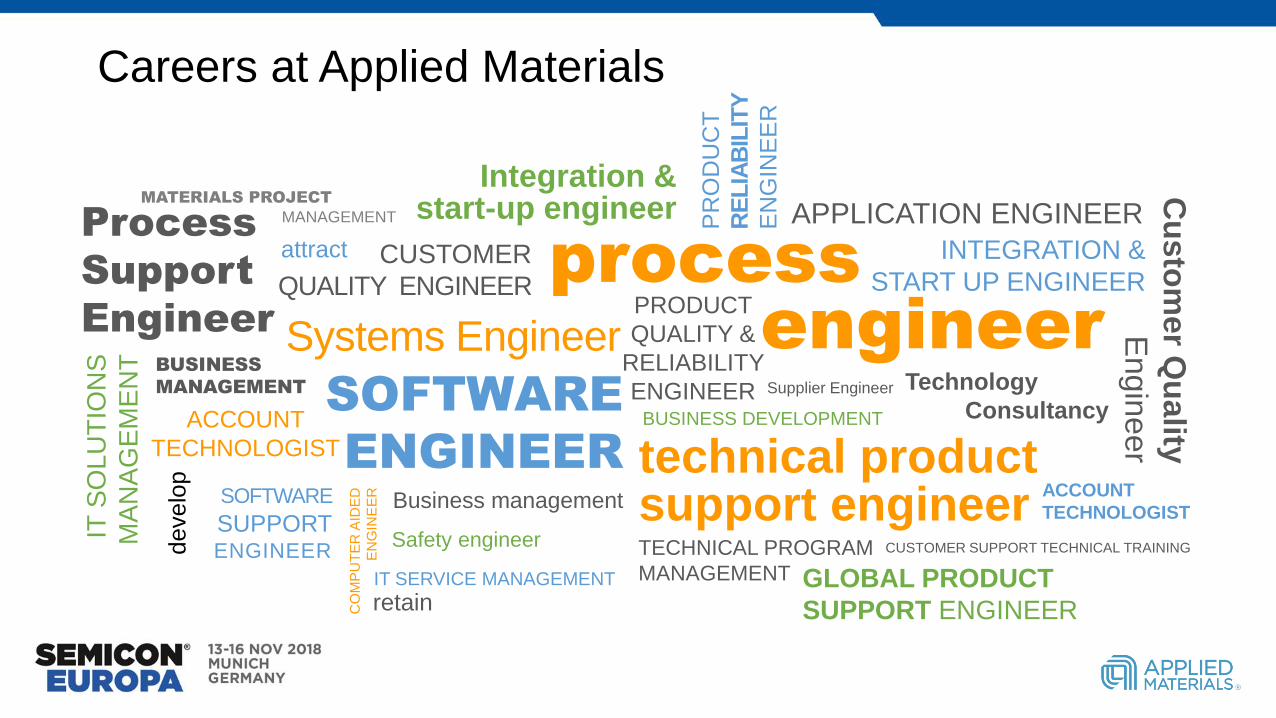
Careers at Applied Materials

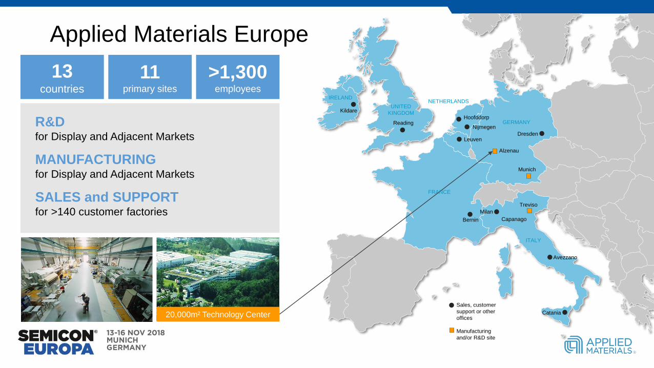
Applied Materials Europe
R&D for Display and Adjacent Markets
MANUFACTURINGfor Display and Adjacent Markets
SALES and SUPPORT for >140 customer factories
13countries
11primary sites
>1,300employees
20,000m² Technology Center
Sales, customer
support or other
offices
Manufacturing
and/or R&D site
Treviso
CapanagoBernin
Reading
Kildare
Hoofddorp
Nijmegen
Alzenau
Avezzano
Catania
Milan
FRANCE
GERMANY
UNITED
KINGDOM
IRELAND
ITALY
NETHERLANDS
DresdenLeuven
Munich

Dresden
Munich
Alzenau
GERMANY
Applied Materials Germany 18
Applied Materials GmbH Dresden
Applied Global Services
Semiconductor
Display
Applied Materials WEB Coating GmbHApplied Materials GmbH & Co. KG.
Applied Materials GmbH Operating Site Feldkirchen
ICT GmbH Heimstetten
AKT Operating Site Feldkirchen
Darmstadt
Mecatronix GmbH

Exciting VUCA Times Ahead
Semiconductors and Displays have
changed the way we live, work and play
Chip performance has increased 106 x
since 1960s…and no slowing down
To enable future technologies, we need
materials engineering solutions
Will You Join Me?