LM1117 Qualification Package
45
800 m A Low-Dropout Linear Regulator You asked – We Made it! an Industry Standard Regulator with Advantage Pricing TM 800 m A Low-Dropout Linear Regulator You asked – We Made it! an Industry Standard Regulator with Advantage Pricing TM LM1117 IN 10μF 4.75V to 5.25V + OUT GND 10μF + V OUT 0-800mA Typical Application LM1117 Qualification Package What can we build for you ?™ What can we build for you ?™
Transcript of LM1117 Qualification Package

800mA
Low-Dr
opout
Linear
Regul
ator
Youask
ed – We
Made it!
anInd
ustry
Standa
rd
Regula
torwit
h
Advant
age Pr
icing
TM
800mA
Low-Dr
opout
Linear
Regul
ator
Youask
ed – We
Made it!
anInd
ustry
Standa
rd
Regula
torwit
h
Advant
age Pr
icing
TM
LM1117IN
10µF
4.75Vto
5.25V
+
OUTGND
10µF+
VOUT0-800mA
Typical
Application
LM1117Qualification Package
What can we build for you?™
What can we build for you?™

LM1117
QUALIFICATION PACKAGE
Summer 1998

Table ofContents
1.0 Introduction . . . . . . . . . . . . . . . . . . . . . . . . . . . . . . . . 1-1
2.0 Device Information
2.1 Datasheet. . . . . . . . . . . . . . . . . . . . . . . . . . . . . . . . . . . . . . . . . . . 2-1
3.0 Process Information
3.1 Process Details. . . . . . . . . . . . . . . . . . . . . . . . . . . . . . . . . . . . . . 3-13.2 Process Flow & Masks . . . . . . . . . . . . . . . . . . . . . . . . . . . . . . . 3-1
4.0 Packaging Information
4.1 Package Material . . . . . . . . . . . . . . . . . . . . . . . . . . . . . . . . . . . . 4-14.2 Tape and Reel Dimensions . . . . . . . . . . . . . . . . . . . . . . . . . . . . 4-24.3 Die Photo . . . . . . . . . . . . . . . . . . . . . . . . . . . . . . . . . . . . . . . . . . . 4-44.4 Bonding Diagrams . . . . . . . . . . . . . . . . . . . . . . . . . . . . . . . . . . . 4-5
5.0 Reliability Data
5.1 Reliability Report . . . . . . . . . . . . . . . . . . . . . . . . . . . . . . . . . . . . 5-1
6.0 Characterization Data
6.1 Test Summaries. . . . . . . . . . . . . . . . . . . . . . . . . . . . . . . . . . . . . . 6-1

1.0 INTRODUCTION

1-1LM1117 Qualification Package
1.0 INTRODUCTION
1.1 General Product DescriptionNational Semiconductor Corporation’s LM1117 is, for most applications, a low cost alternative to severalother quasi-low dropout (quasi-LDO) regulators which are currently available. The device is produced infour voltage options: 5.0V, 3.3V, 2.85V, adjustable. Its operation is guaranteed at junction temperaturesranging from 0°C to 125°C. There are two package types available: TO-220 and SOT-223. The packagedrawings are contained in the datasheet, which is included as part of this booklet. The variousproduct/package combinations are listed below.
Output Voltage Full Device Name Packaging Details
5.0V LM1117T-5.0 TO-220LM1117MP-5.0 SOT-223, 250 units/reelLM1117MPX-5.0 SOT-223, 2000 units/reel
3.3V LM1117T-3.3 TO-220LM1117MP-3.3 SOT-223, 250 units/reelLM1117MPX-3.3 SOT-223, 2000 units/reel
2.85V LM1117T-2.85 TO-220LM1117MP-2.85 SOT-223, 250 units/reelLM1117MPX-2.85 SOT-223, 2000 units/reel
Adjustable LM1117T-ADJ TO-220LM1117MP-ADJ SOT-223, 250 units/reel LM1117MPX-ADJ SOT-223, 2000 units/reel
The LM1117 is fabricated using National’s bipolar LB300 process. Fabrication steps are summarized insection 3-2 of this booklet. The four output voltage options are processed identically except that eachreceives a unique metal mask. The die size is 80 mils x 50 mils. For a more detailed description of thefabrication process refer to section 3-0.
1.2 Reliability/Qualification OverviewThe LM1117 was qualified almost entirely in the 3.3V option in SOT-223 (i.e. LM1117MP-3.3). The SOT-223was chosen because it is the most commonly used package in this device’s application. The other optionswere qualified by extension. Only the electrostatic discharge (ESD) testing was done in TO-220. Pleaserefer to section 5-1 for details regarding the qualification.
1.3 Technical AssistanceProduct Engineer
James Dreyfusemail: [email protected]: 408.721.2721
Application Engineers
Dong-mei Yanemail: [email protected]: 408.721.3501

2.0 DEVICE INFORMATION

2-1LM1117 Qualification Package
2.0 DEVICE INFORMATION
LM1117800mA Low-Dropout Linear RegulatorGeneral DescriptionThe LM1117 is a series of low dropout voltage regulatorswith a dropout of 1.2V at 800mA of load current. It has thesame pin-out as National Semiconductor’s industry standardLM317.
The LM1117 is available in an adjustable version, which canset the output voltage from 1.25V to 13.8V with only two ex-ternal resistors. In addition, it is also available in three fixedvoltages, 2.85V, 3.3V, and 5V.
The LM1117 offers current limiting and thermal shutdown. Itscircuit includes a zener trimmed bandgap reference to as-sure output voltage accuracy to within ±1%.
The LM1117 series is available in SOT-223 and TO-220packages. A minimum of 10µF tantalum capacitor is requiredat the output to improve the transient response and stability.
Featuresn Available in 2.85V, 3.3V, 5V, and Adjustable Versionsn Space Saving SOT-223 Packagen Current Limiting and Thermal Protectionn Output Current 800mAn Temperature Range 0˚C to 125˚Cn Line Regulation 0.2% (Max)n Load Regulation 0.4% (Max)
Applicationsn 2.85V Model for SCSI-2 Active Terminationn Post Regulator for Switching DC/DC Convertern High Efficiency Linear Regulatorsn Battery Chargern Battery Powered Instrumentation
Typical Application
Active Terminator for SCSI-2 Bus
DS100919-5
Fixed Output Regulator
DS100919-28
June 1998
LM1117
800mA
Low-D
ropoutLinearR
egulator
© 1998 National Semiconductor Corporation DS100919 www.national.com

2-2
2.0 DEVICE INFORMATION
Ordering Information
PackageTemperature Range
Packaging Marking Transport Media NSC Drawing0˚C to +125˚C
3-lead SOT-223 LM1117MPX-ADJ N03A Tape and Reel MA04A
LM1117MPX-2.85 N04A Tape and Reel
LM1117MPX-3.3 N05A Tape and Reel
LM1117MPX-5.0 N06A Tape and Reel
3-lead TO-220 LM1117T-ADJ LM1117T-ADJ Rails T03B
LM1117T-2.85 LM1117T-2.85 Rails
LM1117T-3.3 LM1117T-3.3 Rails
LM1117T-5.0 LM1117T-5.0 Rails
Block Diagram
DS100919-1
www.national.com 2

2-3LM1117 Qualification Package
2.0 DEVICE INFORMATION
Connection Diagrams
SOT-223
DS100919-4
Top View
TO-220
DS100919-2
Top View
3 www.national.com

2-4
2.0 DEVICE INFORMATION
Absolute Maximum Ratings (Note 1)
If Military/Aerospace specified devices are required,please contact the National Semiconductor Sales Office/Distributors for availability and specifications.
Maximum Input Voltage (VIN to GND)
LM1117-ADJ, LM1117-3.3,LM1117-5.0 20V
Power Dissipation (Note 2) Internally Limited
Junction Temperature (TJ )(Note 2)
150˚C
Storage Temperature Range -65˚C to 150˚C
Lead Temperature
TO-220 (T) PackageSOT-223 (IMP) Package
260˚C, 10 sec260˚C, 4 sec
ESD Tolerance (Note 3) 2000V
Operating Ratings (Note 1)
Input Voltage (VIN to GND)
LM1117-ADJ, LM1117-3.3,LM1117-5.0
15V
LM1117-2.85 10V
Junction Temperature Range (T J)(Note 2)
0˚C to 125˚C
Electrical CharacteristicsTypicals and limits appearing in normal type apply for T J = 25˚C. Limits appearing in Boldface type apply over the entire junc-tion temperature range for operation, 0˚C to 125˚C.
Symbol Parameter Conditions Min(Note 5)
Typ(Note 4)
Max(Note 5) Units
VREF Reference Voltage LM1117-ADJIOUT=10mA, VIN-VOUT=2V, TJ=25˚C10mA≤I OUT≤ 800mA, 1.4V≤VIN-VOUT≤10V
1.2381.225
1.2501.250
1.2621.270
VV
VOUT Output Voltage LM1117-2.85IOUT =10mA, VIN=4.85V, TJ=25˚CO≤I OUT≤800mA, 4.25V≤ VIN≤10VO≤IOUT ≤500mA, VIN=4.10V
2.8202.7902.790
2.8502.8502.850
2.8802.9102.910
VVV
LM1117-3.3I OUT=10mA, VIN=5V TJ=25˚CO≤I OUT≤800mA, 4.75V≤ VIN≤10V
3.2673.235
3.3003.300
3.3333.365
VV
LM1117-5.0I OUT=10mA, VIN=7V, TJ=25˚CO≤I OUT≤ 800mA, 6.5V≤ VIN≤12V
4.9504.900
5.0005.000
5.0505.100
VV
∆VOUT Line Regulation(Note 6)
LM1117-ADJIOUT=10mA, 1.5V≤ VIN-VOUT≤13.75V 0.035 0.2 %
LM1117-2.85I OUT=0mA, 4.25V≤ VIN≤10V 1 6 mV
LM1117-3.3I OUT=0mA, 4.75V≤ VIN≤15V 1 6 mV
LM1117-5.0I OUT=0mA, 6.5V≤ VIN≤15V 1 10 mV
∆V OUT Load Regulation(Note 6)
LM1117-ADJVIN-V OUT=3V, 10≤IOUT≤800mA 0.2 0.4 %
LM1117-2.85V IN=4.25V, 0≤IOUT≤800mA 1 10 mV
LM1117-3.3V IN=4.75V, 0≤IOUT≤800mA 1 10 mV
LM1117-5.0V IN=6.5V, 0≤IOUT≤800mA 1 15 mV
VIN-V OUT Dropout Voltage(Note 7)
IOUT=100mA 1.10 1.20 V
IOUT=500mA 1.15 1.25 V
IOUT=800mA 1.20 1.30 V
ILIMIT Current Limit VIN-VOUT=5V, TJ=25˚C 800 1200 1500 mA
Minimum LoadCurrent (Note 8)
LM1117-ADJVIN=15V 1.7 5 mA
www.national.com 4

2-5LM1117 Qualification Package
2.0 DEVICE INFORMATION
Electrical Characteristics (Continued)
Typicals and limits appearing in normal type apply for T J = 25˚C. Limits appearing in Boldface type apply over the entire junc-tion temperature range for operation, 0˚C to 125˚C.
Symbol Parameter Conditions Min(Note 5)
Typ(Note 4)
Max(Note 5) Units
Quiescent Current LM1117-2.85VIN≤10V 5 10 mA
LM1117-3.3V IN≤15V 5 10 mA
LM1117-5.0V IN≤15V 5 10 mA
Thermal Regulation TA=25˚C, 30ms Pulse 0.01 0.1 %/W
Ripple Regulation fRIPPLE=120Hz, V IN-VOUT=3VVRIPPLE=1VPP
60 75 dB
Adjust Pin Current 60 120 µA
Adjust Pin CurrentChange
10≤ IOUT≤ 800mA,1.4V≤ VIN-VOUT≤ 10V 0.2 5 µA
Temperature Stability 0.5 %
Long Term Stability TA=125˚C, 1000Hrs 0.3 %
RMS Output Noise (% of VOUT), 10Hz≤f≤10kHz 0.003 %
Thermal ResistanceJunction-to-Case
3-Lead SOT-2233-Lead TO-220
15.03.0
˚C/W˚C/W
Thermal ResistanceJunction-to-Ambient(No heat sink;No air flow)
3-Lead SOT-2233-Lead TO-220
13679
˚C/W˚C/W
Note 1: Absolute Maximum Ratings indicate limits beyond which damage to the device may occur. Operating Ratings indicate conditions for which the device is in-tended to be functional, but specific performance is not guaranteed. For guaranteed specifications and the test conditions, see the Electrical Characteristics.
Note 2: The maximum power dissipation is a function of TJ(max) , θJA, and TA. The maximum allowable power dissipation at any ambient temperature is PD = (TJ-
(max)–T A)/θJA. All numbers apply for packages soldered directly into a PC board.
Note 3: For testing purposes, ESD was applied using human body model, 1.5kΩ in series with 100pF.
Note 4: Typical Values represent the most likely parametric norm.
Note 5: All limits are guaranteed by testing or statistical analysis.
Note 6: Load and line regulation are measured at constant junction room temperature.
Note 7: The dropout voltage is the input/output differential at which the circuit ceases to regulate against further reduction in input voltage. It is measured when theoutput voltage has dropped 100mV from the nominal value obtained at VIN=V OUT+1.5V.
Note 8: The minimum output current required to maintain regulation.
5 www.national.com

2-6
2.0 DEVICE INFORMATION
Typical Performance Characteristics
Dropout Voltage (V IN-V OUT)
DS100919-22
Short-Circuit Current
DS100919-23
Load Regulation
DS100919-24
LM1117-ADJ Ripple Rejection
DS100919-6
LM1117-ADJ Ripple Rejection vs. Current
DS100919-7
Temperature Stability
DS100919-25
www.national.com 6

2-7LM1117 Qualification Package
2.0 DEVICE INFORMATION
Typical Performance Characteristics (Continued)
Adjust Pin Current
DS100919-26
LM1117-2.85 Load Transient Response
DS100919-8
LM1117-5.0 Load Transient Response
DS100919-9
LM1117-2.85 Line Transient Response
DS100919-10
LM1117-5.0 Line Transient Response
DS100919-11
7 www.national.com

2-8
2.0 DEVICE INFORMATION
APPLICATION NOTE1.0 External Capacitors/Stability
1.1 Input Bypass Capacitor
An input capacitor is recommended. A 10µF tantalum on theinput is a suitable input bypassing for almost all applications.
1.2 Adjust Terminal Bypass Capacitor
The adjust terminal can be bypassed to ground with a by-pass capacitor (CADJ) to improve ripple rejection. This by-pass capacitor prevents ripple from being amplified as theoutput voltage is increased. At any ripple frequency, the im-pedance of the CADJ should be less than R1 to prevent theripple from being amplified:
1/(2π*fRIPPLE*CADJ) < R1
The R1 is the resistor between the output and the adjust pin.Its value is normally in the range of 100-200Ω. For example,with R1=124Ω and fRIPPLE=120Hz, the CADJ should be 11µF.
1.3 Output Capacitor
The output capacitor is critical in maintaining regulator stabil-ity, and must meet the required conditions for both minimumamount of capacitance and ESR (Equivalent Series Resis-tance). The minimum output capacitance required by theLM1117 is 10µF, if a tantalum capacitor is used. Any increaseof the output capacitance will merely improve the loop stabil-ity and transient response. The ESR of the output capacitorshould be less than 0.5Ω. In the case of the adjustable regu-lator, when the C ADJ is used, a larger output capacitance(22µf tantalum) is required.
2.0 Output Voltage
The LM1117 adjustable version develops a 1.25V referencevoltage, VREF, between the output and the adjust terminal.As shown in Figure 1, this voltage is applied across resistorR1 to generate a constant current I1. The current IADJ fromthe adjust terminal could introduce error to the output. Butsince it is very small (60µA) compared with the I1 and veryconstant with line and load changes, the error can be ig-nored. The constant current I1 then flows through the outputset resistor R2 and sets the output voltage to the desiredlevel.
For fixed voltage devices, R1 and R2 are integrated insidethe devices.
3.0 Load Regulation
The LM1117 regulates the voltage that appears between itsoutput and ground pins, or between its output and adjustpins. In some cases, line resistances can introduce errors tothe voltage across the load. To obtain the best load regula-tion, a few precautions are needed.
Figure 2 shows a typical application using a fixed outputregulator. The Rt1 and Rt2 are the line resistances. It is ob-vious that the V LOAD is less than the VOUT by the sum of thevoltage drops along the line resistances. In this case, theload regulation seen at the RLOAD would be degraded fromthe data sheet specification. To improve this, the load shouldbe tied directly to the output terminal on the positive side anddirectly tied to the ground terminal on the negative side.
When the adjustable regulator is used (Figure 3), the bestperformance is obtained with the positive side of the resistorR1 tied directly to the output terminal of the regulator ratherthan near the load. This eliminates line drops from appearingeffectively in series with the reference and degrading regula-tion. For example, a 5V regulator with 0.05Ω resistance be-tween the regulator and load will have a load regulation dueto line resistance of 0.05Ω x IL. If R1 (=125Ω) is connectednear the load, the effective line resistance will be 0.05Ω(1+R2/R1) or in this case, it is 4 times worse. In addition, theground side of the resistor R2 can be returned near theground of the load to provide remote ground sensing and im-prove load regulation.
4.0 Protection Diodes
Under normal operation, the LM1117 regulators do not needany protection diode. With the adjustable device, the internalresistance between the adjust and output terminals limits thecurrent. No diode is needed to divert the current around theregulator even with capacitor on the adjust terminal. The ad-just pin can take a transient signal of ±25V with respect tothe output voltage without damaging the device.
When a output capacitor is connected to a regulator and theinput is shorted to ground, the output capacitor will discharge
DS100919-17
Figure 1. Basic Adjustable Regulator
DS100919-18
Figure 2. Typical Application using Fixed OutputRegulator
DS100919-19
Figure 3. Best Load Regulation using AdjustableOutput Regulator
www.national.com 8

2-9LM1117 Qualification Package
2.0 DEVICE INFORMATION
APPLICATION NOTE (Continued)
into the output of the regulator. The discharge current de-pends on the value of the capacitor, the output voltage of theregulator, and rate of decrease of V IN. In the LM1117 regu-lators, the internal diode between the output and input pinscan withstand microsecond surge currents of 10A to 20A.With an extremely large output capacitor (≥1000 µF), andwith input instantaneously shorted to ground, the regulatorcould be damaged.
In this case, an external diode is recommended between theoutput and input pins to protect the regulator, as shown inFigure 4.
5.0 Heatsink Requirements
The LM1117 regulators have internal thermal shutdown toprotect the device from over-heating. Under all possible op-erating conditions, the junction temperature of the LM1117must be within the range of 0˚C to 125˚C. A heatsink may berequired depending on the maximum power dissipation and
maximum ambient temperature of the application. To deter-mine if a heatsink is needed, the power dissipated by theregulator, PD , must be calculated:
IIN = IL + IGPD = (VIN-VOUT)I L + VINIG
Figure 5 shows the voltages and currents which are presentin the circuit.
The next parameter which must be calculated is the maxi-mum allowable temperature rise, TR(max):
TR(max)=TJ(max)-TA(max)
where TJ(max) is the maximum allowable junction tempera-ture (125˚C), and TA(max) is the maximum ambient tem-perature which will be encountered in the application.
Using the calculated values for TR(max) and P D, the maxi-mum allowable value for the junction-to-ambient thermal re-sistance (θJA) can be calculated:
θJA = TR(max)/PD
If the maximum allowable value for θJA is found to be≥136˚C/W for SOT-223 package or ≥79˚C/W for TO-220package, no heatsink is needed since the package alone willdissipate enough heat to satisfy these requirements. If thecalculated value for θJA falls below these limits, a heatsink isrequired.
As a design aid, Table 1 shows the value of the θ JA of SOT-223 for different heatsink area. The copper patterns that weused to measure these θJAs are shown at the end of the Ap-plication Notes Section. Figure 6 reflects the same test re-sults as what are in the Table 1.
Table 1. θJA of SOT-223 for Different Heatsink AreaLayout 1oz Copper Area Thermal Resistance
Top Side (in2)* Bottom Side (in2) (θJA,˚C/W)
1 0.0123 0 136
2 0.066 0 123
3 0.3 0 84
4 0.53 0 75
5 0.76 0 69
6 1 0 66
7 0 0.2 115
8 0 0.4 98
9 0 0.6 89
10 0 0.8 82
11 0 1 79
12 0.066 0.066 125
13 0.175 0.175 93
14 0.284 0.284 83
DS100919-15
Figure 4. Regulator with Protection Diode
DS100919-16
Figure 5. Power Dissipation Diagram
9 www.national.com

2-10
2.0 DEVICE INFORMATION
APPLICATION NOTE (Continued)
Table 1. θJA of SOT-223 for Different Heatsink Area (Continued)
Layout 1oz Copper Area Thermal Resistance
15 0.392 0.392 75
16 0.5 0.5 70
*Tab of device attached to topside copper
Figure 7 shows the maximum allowable power dissipationvs. ambient temperature for the SOT-223 device. Figure 8shows the maximum allowable power dissipation vs. 1ozcopper area (in2) for the SOT-223 device. Please seeAN1028 for power enhancement techniques to be used withSOT-223 package.
DS100919-13
Figure 6. θJA vs. 1oz Copper Area
DS100919-12
Figure 7. Maximum Allowable Power Dissipation vs.Ambient Temperature
DS100919-14
Figure 8. Maximum Allowable Power Dissipation vs.1oz Copper Area
www.national.com 10

2-11LM1117 Qualification Package
2.0 DEVICE INFORMATION
APPLICATION NOTE (Continued)
DS100919-20
Figure 9. Top View of the SOT-223 Thermal Test Pattern in Actual Scale
11 www.national.com

2-12
2.0 DEVICE INFORMATION
APPLICATION NOTE (Continued)
DS100919-21
Figure 10. Bottom View of the SOT-223 Thermal Test Pattern in Actual Scale
www.national.com 12

2-13LM1117 Qualification Package
2.0 DEVICE INFORMATION
Typical Application Circuits
DS100919-30
Adjusting Output of Fixed Regulators
DS100919-31
Regulator with Reference
DS100919-29
1.25V to 10V Adjustable Regulator with ImprovedRipple Rejection
DS100919-27
5V Logic Regulator with Electronic Shutdown*
DS100919-32
Battery Backed-Up Regulated Supply
13 www.national.com

2-14
2.0 DEVICE INFORMATION
Typical Application Circuits (Continued)
DS100919-33
Low Dropout Negative Supply
www.national.com 14

2-15LM1117 Qualification Package
2.0 DEVICE INFORMATION
Physical Dimensions inches (millimeters) unless otherwise noted
3-Lead SOT-223 PackageOrder Number LM1117MPX-ADJ, LM1117MPX-2.85, LM1117MPX-3.3, or LM1117MPX-5.0
NSC Package Number MA04A
15 www.national.com

2-16
2.0 DEVICE INFORMATION
Physical Dimensions inches (millimeters) unless otherwise noted (Continued)
LIFE SUPPORT POLICY
NATIONAL’S PRODUCTS ARE NOT AUTHORIZED FOR USE AS CRITICAL COMPONENTS IN LIFE SUPPORT DE-VICES OR SYSTEMS WITHOUT THE EXPRESS WRITTEN APPROVAL OF THE PRESIDENT OF NATIONAL SEMI-CONDUCTOR CORPORATION. As used herein:1. Life support devices or systems are devices or sys-
tems which, (a) are intended for surgical implant intothe body, or (b) support or sustain life, and whose fail-ure to perform when properly used in accordancewith instructions for use provided in the labeling, canbe reasonably expected to result in a significant injuryto the user.
2. A critical component in any component of a life supportdevice or system whose failure to perform can be rea-sonably expected to cause the failure of the life supportdevice or system, or to affect its safety or effectiveness.
National SemiconductorCorporationAmericasTel: 1-800-272-9959Fax: 1-800-737-7018Email: [email protected]
www.national.com
National SemiconductorEurope
Fax: +49 (0) 1 80-530 85 86Email: [email protected]
Deutsch Tel: +49 (0) 1 80-530 85 85English Tel: +49 (0) 1 80-532 78 32Français Tel: +49 (0) 1 80-532 93 58Italiano Tel: +49 (0) 1 80-534 16 80
National SemiconductorAsia Pacific CustomerResponse GroupTel: 65-2544466Fax: 65-2504466Email: [email protected]
National SemiconductorJapan Ltd.Tel: 81-3-5620-6175Fax: 81-3-5620-6179
3-Lead TO-220 PackageOrder Number LM1117T-ADJ, LM1117T-2.85, LM1117T-3.3, or LM1117T-5.0
NSC Package Number T03B
LM11
1780
0mA
Low
-Dro
pout
Line
arR
egul
ator
National does not assume any responsibility for use of any circuitry described, no circuit patent licenses are implied and National reserves the right at any time without notice to change said circuitry and specifications.
3.0 PROCESS INFORMATION

3-1LM1117 Qualification Package
3.0 PROCESS INFORMATION
3.1 PROCESS DETAILSFabrication Site: Greenock, ScotlandProcess Technology: LB300 (Bipolar)Wafer Diameter: 6 inches (150 mm)Number of Masks: 11Metallization: Al with 0.5% CuTop Side Passivation: Oxide/Nitride
3.2 PROCESS FLOW AND MASKS1: Laser Scribe2: Initial Oxide3: Collector Mask4: Collector Implant5: Collector Diffusion6: Iso-Up Mask7: Iso-Up Implant8: Strip/Inspect9: Epi Growth
10: Epi Reox11: Plug Mask12: Plug PreDep13: Plug Diffusion14: Iso Down Mask15: Pre Iso-Down Implant Ox16: Iso Down Implant17: Iso Down Diffusion18: FTA mask19: FTA Implant20: FTA Reox21: Base Mask22: Pre Base Implant Ox23: Base Implant24: Base Diffusion
25: Post Base Ox26: Emitter Mask27: Iso/CB Diode Check28: Screen Ox29: Emitter Implant30: Emitter Diffusion31: Resistor Mask32: Resistor Implant33: VOE (Vapox Over Emitter)34: Getter35: Capacitor Ox36: Anneal37: Contact Mask38: Platinum Depostion39: Platinum Silicide40: Platinum Strip41: Titanium Tungsten Sputter42: Metal Deposition43: Metal Mask44: Passivation45: Passivation Mask46: Anneal47: Electrical Test

3.0 PROCESS INFORMATION

4.0 PACKAGING INFORMATION
4-1LM1117 Qualification Package
4.0 PACKAGING INFORMATION
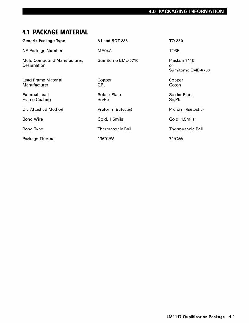
4.1 PACKAGE MATERIALGeneric Package Type 3 Lead SOT-223 TO-220
NS Package Number MA04A TO3B
Mold Compound Manufacturer, Sumitomo EME-6710 Plaskon 7115 Designation or
Sumitomo EME-6700
Lead Frame Material Copper CopperManufacturer QPL Gotoh
External Lead Solder Plate Solder PlateFrame Coating Sn/Pb Sn/Pb
Die Attached Method Preform (Eutectic) Preform (Eutectic)
Bond Wire Gold, 1.5mils Gold, 1.5mils
Bond Type Thermosonic Ball Thermosonic Ball
Package Thermal 136°C/W 79°C/W

4-2
4.0 PACKAGING INFORMATION
4.2 TAPE & REEL DIMENSIONS

4-3LM1117 Qualification Package
4.0 PACKAGING INFORMATION

4-4
4.0 PACKAGING INFORMATION
4.3 DIE PHOTO
80mils
50mils

4-5LM1117 Qualification Package
4.0 PACKAGING INFORMATION
4.4 BONDING DIAGRAMS

4-6
4.0 PACKAGING INFORMATION

4-7LM1117 Qualification Package
4.0 PACKAGING INFORMATION

4-8
4.0 PACKAGING INFORMATION

4-9LM1117 Qualification Package
4.0 PACKAGING INFORMATION

4-10
4.0 PACKAGING INFORMATION

4-11LM1117 Qualification Package
4.0 PACKAGING INFORMATION

4-12
4.0 PACKAGING INFORMATION

5.0 RELIABILITY DATA

5-1LM1117 Qualification Package
5.0 RELIABILITY DATA
Reliability Test Report
File Number:FSC19980214
Originator:Nick Stanco
Date:May 14, 1998
LM1117 NEW DEVICE QUALIFICATION
Purpose Approvals
RSC199801268RSC199801267RSC199800916REM199800705Q19970942
Reference File Numbers
Jim DreyfusNick Stanco
Distribution List
The LM1117 800 mA Low Drop Out Voltage Regulator fabricated on the NSUK LB300 process was sub-jected to reliability testing per qual Q19970942 for qualification as a new device. All required reliabilitytesting has been completed without the occurrence of a single failure. Based on these results theLM1117 is now fully qualified and released to production in the 3L SOT-223 and TO-220 packages and inall voltage options.
Abstract
Test Request Device Name Sbgp Loc Fab Line Pkg Code # Leads Loc Date Cd Mold Cmpd
RSC199801267 LM1117MP A UK 6 INCH T\MSON 3 EM 9252 B18RSC199801268 LM1117MP-ADJ A UK 6 INCH T\P223 3 EM 9252 B18REM199800705 LM1117MP A UK 6 INCH T\MSON 3 EM 9806 B18REM199800705 LM1117MP B UK 6 INCH T\MSON 3 EM 9806 B18REM199800705 LM1117MP C UK 6 INCH T\MSON 3 EM 9806 B18RSC199800916 LM1117MP A UK 6 INCH T\MSON 3 EM 9806 B18
Description
Test: Electrostatic Discharge - Human Body Model (ESDH)Test Request Device MethodRSC199801267 LM1117MP ATERSC199801268 LM1117MP-ADJ ATE
Test: Electrostatic Discharge - Machine Model (ESDM)Test Request Device MethodRSC199801267 LM1117MP ATERSC199801268 LM1117MP-ADJ ATE
Tests Performed
Reliability Engineer
Mgr Ref Engineering

5-2
5.0 RELIABILITY DATA
Test: Autoclave Test (ACLV)Test Request Device Sbgrp Rel Humidity Pressure High Temp LowTempREM199800705 LM1117MP A 100 15 121 -REM199800705 LM1117MP B 100 15 121 -REM199800705 LM1117MP C 100 15 121 -
Test: Operating Life Test (Static) (SOPL)Test Request Device Sbgrp Rel Humidity Pressure High Temp LowTempREM199800705 LM1117MP A - - 125 -REM199800705 LM1117MP B - - 125 -REM199800705 LM1117MP C - - 125 -
Test: Power Cycle (PRCL)Test Request Device Sbgrp Rel Humidity Pressure High Temp LowTempRSC199800916 LM1117MP A 150 25
Test: Temperature Cycle (TMCL)Test Request Device Sbgrp Rel Humidity Pressure High Temp LowTempREM199800705 LM1117MP A - - 150 -65REM199800705 LM1117MP B - - 150 -65REM199800705 LM1117MP C - - 150 -65
Test: Temperature Humidity Bias Test (THBT)Test Request Device Sbgrp Rel Humidity Pressure High Temp LowTempREM199800705 LM1117MP A 85 - 85 -REM199800705 LM1117MP B 85 - 85 -REM199800705 LM1117MP C 85 - 85 -
Test: Preconditioning (all units were preconditioned per RAI-5-039 using a Level 1 85C/85% RH 168 hour moisturesoak and 235C IR reflow)
Tests Performed (cont)
Rejects per Lot Sample Size
Tests Time/Cycles Lot 1 Lot 2 Lot 3
SOPL-IB1 168 hours 0/77 0/77 0/77500 hours 0/77 0/77 0/771000 hours 0/77 0/77 -----
THBT-IB1 168 hours 0/77500 hours 0/771000 hours 0/77
ACLV-IB1 96 hours 0/77168 hours 0/77
TMCL-IB1 500 cycles 0/771000 cycles 0/77
PRCL-IB1 3000 cycles 0/77
Results

5-3LM1117 Qualification Package
5.0 RELIABILITY DATA
HBM ESD LM1117MP-ADJ LM1117MP-3.3
500 volts 0/5 500 volts 0/51000 volts 0/5 1000 volts 0/51500 volts 0/5 1500 volts 0/52000 volts 0/5 2000 volts 0/5
MM ESD LM1117MP-ADJ LM1117MP-3.3
50 volts 0/5 50 volts 0/5100 volts 0/5 100 volts 0/5150 volts 0/5 150 volts 0/5200 volts 0/5 200 volts 0/5
Results (cont)
The LM1117 is now fully qualified and released to production in the 3L SOT-223 and TO-220 packagesand in all voltage options.
Conclusion

6.0 CHARACTERIZATION DATA

6-1
LM1117-ADJ Typical Units Mean Sigma
Reference Voltage, Vin - Vout = 2V, Iout = 10mA V 1.252 0.003
Reference Voltage, Vin - Vout = 1.4V, Iout = 1 mA V 1.252 0.003
Reference Voltage, Vin - Vout = 1.4V, Iout = 800mA V 1.250 0.003
Reference Voltage, Vin - Vout = 10V, Iout =10mA V 1.252 0.003
Reference Voltage, Vin - Vout = 10V, Iout =100mA V 1.251 0.003
Line Regulation, 1.5V < Vin - Vout < 13.75V, Iout = 10mA % -0.004 0.013
Load Regulation, Vin - Vout = 3.0V, 10mA < Iout < 800mA % 0.175 0.025
Dropout Voltage, Iout = 100mA Refer to LM1117-3.3V Data
Dropout Voltage, Iout = 500mA Refer to LM1117-3.3V Data
Dropout Voltage, Iout = 80 mA Refer to LM1117-3.3V Data
Current Limit mA 1177 17.9
Thermal Regulation, Vin - Vout = 10V, Iout = 100mA, 30 sec Pulse % 0.006 0.023
Minimum Load Current mA 1.052 0.0315
Adjust Pin Current uA 55.1 1.1
Adjust Pin Current Change, Vin - Vout = 1.4V, 10mA < Iout < 800mA uA -0.236 0.143
LM1117-5.0 Typical Units Mean Sigma
Output Voltage, Vin = 6.5V, Iout = 0mA V 5.005 0.020
Output Voltage, Vin =6.5V, Iout = 800mA V 5.003 0.020
Output Voltage, Vin = 7.0V, Iout = 10mA V 5.005 0.020
Output Voltage, Vin = 12V, Iout = 0mA V 5.006 0.020
Output Voltage, Vin = 12V, Iout = 100mA V 5.004 0.020
Line Regulation, 6.5V < Vin < 15V, Iout = 0mA mV 0.395 0.238
Load Regulation, Vin = 6.5V, 0 < Iout < 800mA mV 1.638 1.108
Dropout Voltage, Iout = 100mA Refer to LM1117-3.3V Data
Dropout Voltage, Iout = 500mA Refer to LM1117-3.3V Data
Dropout Voltage, Iout = 800mA Refer to LM1117-3.3V Data
Thermal Regulation, Vin - Vout = 10V, Iout = 100 mA, 30 sec Pulse % -0.001 0.007
Current Limit mA 1312 28.6
Quiescent Current, Vin < 15V mA 5.749 0.069
LM1117 Qualification Package
6.0 CHARACTERIZATION DATA
6.1 TEST SUMMARIES

6-2
6.0 CHARACTERIZATION DATA
LM1117-2.85 Typical Units Mean Sigma
Output Voltage, Vin = 4.85V, Iout = 10mA V 2.857 0.007
Output Voltage, Vin = 4.25V, Iout = 0mA V 2.857 0.007
Output Voltage, Vin = 4.10V, Iout = 0mA V 2.857 0.007
Output Voltage, Vin = 10V, Iout = 0mA V 2.857 0.007
Output Voltage, Vin = 10V, Iout = 100mA V 2.856 0.007
Output Voltage, Vin =4.10V, Iout=500mA V 2.856 0.007
Output Voltage, Vin =4.25V, Iout=800mA V 2.855 0.007
Line Regulation, 4.25V < Vin < 10V, Iout = 0mA mV 0.297 0.198
Load Regulation, 0 < Iout < 800mA, Vin = 4.25V mV 1.590 0.347
Dropout Voltage, Iout = 100mA Refer to LM1117-3.3V Data
Dropout Voltage, Iout = 500mA Refer to LM1117-3.3V Data
Dropout Voltage, Iout = 800mA Refer to LM1117-3.3V Data
Thermal Regulation, Vin - Vout = 10V, Iout = 100mA, 30 sec Pulse % 0.028 0.010
Current Limit mA 1212 22.8
Quiescent Current mA 5.729 0.098
LM1117-3.3 Typical Units Mean Sigma
Output Voltage, Vin = 5V, Iout = 10mA V 3.309 0.008
Output Voltage, Vin = 4.75V, Iout = 0mA V 3.309 0.008
Output Voltage, Vin = 4.75V, Iout = 800mA V 3.309 0.008
Output Voltage, Vin = 10V, Iout = 0mA V 3.310 0.008
Output Voltage, Vin =10V, Iout = 100mA V 3.308 0.008
Line Regulation, 4.75V < Vin < 15V, Iout = 0mA mV -0.014 0.235
Load Regulation, 0 < Iout < 800 mA, Vin = 4.75V mV 0.738 0.403
Dropout Voltage, Iout = 100mA V 1.032 0.009
Dropout Voltage, Iout = 500mA V 1.171 0.008
Dropout Voltage, Iout = 800mA V 1.189 0.004
Thermal Regulation, Vin - Vout = 10V, Iout = 100mA, 30 sec Pulse % 0.020 0.010
Current Limit mA 1245 28.3
Quiescent Current mA 5.862 0.093