L P -A D F A SING ELF RESETTING LOGIC WITH GDI T
13
International Journal of VLSI design & Communication Systems (VLSICS) Vol.7, No.4, August 2016 DOI : 10.5121/vlsic.2016.7406 57 LOW POWER-AREA DESIGN OF FULL ADDER USING SELF RESETTING LOGIC WITH GDI TECHNIQUE Simran Khokha 1 and K.Rahul Reddy 2 1 ARSD College, Department of Electronics Science, University Of Delhi, New Delhi, India 2 Department of Electronics and Communication Engineering, Sharda University, Greater Noida, U.P, India ABSTRACT Various electronic devices such as mobile phones, DSPs,ALU etc., are designed by using VLSI (Very Large Scale Integration) technology. In VLSI dynamic CMOS logic circuits are concentrating on the Area ,reducing the power consumption and increasing the Speed by reducing the delay. ALU (Arithmetic Logic Circuits) are designed by using adder, subtractors, multiplier, divider, etc.Various adder circuits designs have been proposed over last few years with different logic styles. To reduce the power consumption several parameters are to be taken into account, such as feedthrough, leakage power single-event upsets, charge sharing by parasitic components while connecting source and drain of CMOS transistors There are situations in a logic that permit the use of circuits that can automatically precharge themselves (i.e., reset themselves) after some prescribed delays. These circuits are hence called postcharge or self-resetting logic which are widely used in dynamic logic circuits. Overall performance of various adder designs is evaluated by using Tanner tool . The earlier and the proposed SRLGDI primitives are simulated using Tanner EDA with BSIM 0.250 lm technology with supply voltage ranging from 0 V to 5 V in steps of 0.2 V. On comparing the various SRLGDI logic adders, the proposed adder shows low power, delay and low PDP among its counterparts. KEYWORDS Precharge , Self Resetting Logic, GDI Logic, Dynamic Logic 1. INTRODUCTION Full adder circuit is a basic building block and the most important component of complex arithmetic circuits like microprocessors, digital signal processors, microcontrollers or any ALUs. Almost every complex digital circuit requires full adder circuitry. The entire computational block power consumption, delay as well as no. of transistors can be reduced by implementing low power techniques on full adder circuitry. Several full adder circuits have been proposed targeting on design variations such as power, area and delay. Among those designs with less transistor count using pass transistor logic have been
Transcript of L P -A D F A SING ELF RESETTING LOGIC WITH GDI T

International Journal of VLSI design & Communication Systems (VLSICS) Vol.7, No.4, August 2016
DOI : 10.5121/vlsic.2016.7406 57
LOW POWER-AREA DESIGN OF FULL ADDER
USING SELF RESETTING LOGIC WITH GDI
TECHNIQUE
Simran Khokha1 and K.Rahul Reddy
2
1ARSD College, Department of Electronics Science,
University Of Delhi, New Delhi, India 2Department of Electronics and Communication Engineering,
Sharda University, Greater Noida, U.P, India
ABSTRACT
Various electronic devices such as mobile phones, DSPs,ALU etc., are designed by using VLSI (Very
Large Scale Integration) technology. In VLSI dynamic CMOS logic circuits are concentrating on the Area
,reducing the power consumption and increasing the Speed by reducing the delay. ALU (Arithmetic Logic
Circuits) are designed by using adder, subtractors, multiplier, divider, etc.Various adder circuits designs
have been proposed over last few years with different logic styles. To reduce the power consumption
several parameters are to be taken into account, such as feedthrough, leakage power single-event upsets,
charge sharing by parasitic components while connecting source and drain of CMOS transistors There are
situations in a logic that permit the use of circuits that can automatically precharge themselves (i.e., reset
themselves) after some prescribed delays. These circuits are hence called postcharge or self-resetting logic
which are widely used in dynamic logic circuits. Overall performance of various adder designs is
evaluated by using Tanner tool . The earlier and the proposed SRLGDI primitives are simulated using
Tanner EDA with BSIM 0.250 lm technology with supply voltage ranging from 0 V to 5 V in steps of 0.2 V.
On comparing the various SRLGDI logic adders, the proposed adder shows low power, delay and low
PDP among its counterparts.
KEYWORDS
Precharge , Self Resetting Logic, GDI Logic, Dynamic Logic
1. INTRODUCTION
Full adder circuit is a basic building block and the most important component of complex
arithmetic circuits like microprocessors, digital signal processors, microcontrollers or any ALUs.
Almost every complex digital circuit requires full adder circuitry. The entire computational block
power consumption, delay as well as no. of transistors can be reduced by implementing low
power techniques on full adder circuitry.
Several full adder circuits have been proposed targeting on design variations such as power, area
and delay. Among those designs with less transistor count using pass transistor logic have been

International Journal of VLSI design & Communication Systems (VLSICS) Vol.7, No.4, August 2016
58
widely used to reduce power consumption [2-4]. These designs suffer from severe output signal
degradation and cannot sustain low voltage operations, inspite of the circuit simplicity, [5].
Static complementary metal oxide semiconductor (CMOS) technology has been the ideal choice
of designers in the past years due to its robustness against voltage scaling and transistor sizing.
The main drawbacks of static CMOS are high power dissipation and large propagation delay. The
high power dissipation is due to the fact that the larger number of pMOS transistors end up with
high input loads. The high operating frequency also increases the power dissipation of these
circuits. These concerns arise the need of dynamic CMOS logic circuits for high speed
applications. It offers faster switching speed with reduced load capacitance and requires less
number of transistors and occupies less area. However this circuit suffers from charge leakage,
charge sharing, loss of noise immunity, feedthrough and timing problem due to clock input.
These issues can be resolved using an asynchronous dynamic circuit named Self Resetting logic
(SRL).
In these designs we have exploited the advantages of SRLGDI technique for low power. In
proposed technique the basic idea is to turn off GDI logic circuit or lower down potential across
logic circuits when the circuit is in reset state. To achieve this action we have added a switching
circuit operated by clock which cuts off supply of all GDI gates, inverters and buffers used in
circuit.
The rest of the paper is organised as previous research work, proposed full adder designs,
simulations-results-comparison and conclusion.
1.1 SELF RESETTING LOGIC IN ADDERS
The SRL full adder circuit is shown in Fig. 3. This adder logic consists of sum and carry block.
The sum block is implemented by SRL XOR gates. The carry block is implemented by SRL
AND and SLR OR gates. The input to this full adder logic circuit are A ,B and Cin and the
outputs are S(Sum) and C(Carry).
The output (sum) is obtained by using the expression
The output (sum) is obtained by using the expression
S = ((A XOR B) XOR Cin) (1)
The output (carry) is obtained by using the expression
C = AB + BC + AC (2)

International Journal of VLSI design & Communication Systems (VLSICS) Vol.7, No.4, August 2016
59
Fig.1 SRL Full Adder
The sum output is obtained using two XOR gates and carry output is obtained by using two AND
gates and one OR gate.
2. PREVIOUS WORK
Many different adder circuits’ designs are proposed over last many years with different logic
styles. In [9], low power Carry Look ahead Adder (CLA) is designed using domino logic of
150nm channel length and it is proposed that it is more optimized than other channel lengths.
Sometimes, a sleepy technique or a power gating technique is used to reduce the power.
consumption in the full adder logic circuit, 4-bit adders and 4 -bit binary coded decimal (BCD)
adder circuits. The high speed adder logic circuits proposed in Self resetting logic are re-
configured, thereby the no. of transistors in the proposed design are reduced.
SRL represents signals as short-duration pulses rather than as voltage levels. When a set of pulses
are driven to the inputs to a logic gate, they must reach at the same time and they must overlap
with one another for a minimum duration. After a logic gate has processed a set of input pulses, a
reset signal is activated that restores the logic gate to a state in which it can receive another set of
input pulses. Two types of reset structures have been proposed in the literature. In global SRL ,
the reset signal for each stage is produced by a separate timing chain which yields a parallel
worst-case delay path.
SRL circuit operation comprises of separate precharge and evaluation phase that discharges the
dynamic storage nodes to evaluate the desired logic function. The nodes are reset back to their
original charged state by a local timing. One of the benefits of self-resetting logic is that the data
present at the evaluation phase do not require dynamic node to discharge, which makes the
precharge device inactive, thereby considerably reducing the power. However it suffers from low
output voltage and static power dissipation due to nMOS pull down network and hence makes
conductance overlap between nMOS and pMOS. Sleep transistor logic along with Multi-
threshold CMOS approach is applied to reduce the leakage and dynamic power issues.

International Journal of VLSI design & Communication Systems (VLSICS) Vol.7, No.4, August 2016
60
R.Uma et al. (2013) stated that addition is an indispensable operation for any high speed digital
system, digital signal processing or control system. The primary issues in the design of adder
logic cell are delay, area and power dissipation. Optimization of several devices for power and
speedcis a significant issue in low-voltage and low-power applications. These issues can be
resolved by incorporating Gated Diffusion Input (GDI) technique. This paper mainly presents the
design of 3 different full adder topologies using SRL Gate Diffusion Input Technique. This
technique allows reducing delay, power consumption and area of digital circuits, while
maintaining low complexity of design. This paper focuses two main design approaches. The
former presents the implementation of modified SRL primitive logic cells of XOR, AND,
NAND, NOR, OR, XNOR and its performance comparison with various other logic designed
gates. The latter presents the implementation of 3 different modified SRLGDI full adders
incorporating these SRLGDI gates and its performance comparison. The simulation results
reveal better delay and power performance for the proposed modified SRL GDI full adders
when compared with the existing GDI technique, CMOS and pass transistor logic at 0.250 µm
CMOS technologies. Power, delay and PDP has been evaluated by Tanner simulator using
TSMC BSIM 0.250 µm technologies.
2.1 PRIMITIVE CELL DESIGN IN SRLGDI LOGIC
Fig. 2 2-Input primitive cells in SRL with gate diffusion input level restoration buffer. (a) AND gate,
(b) OR gate, (c) NAND gate, (d) NOR gate, (e) XOR gate and (f) XNOR gate.

International Journal of VLSI design & Communication Systems (VLSICS) Vol.7, No.4, August 2016
61
Fig.2 Design of R.Uma et al (2015) [1]

International Journal of VLSI design & Communication Systems (VLSICS) Vol.7, No.4, August 2016
62
3. DESIGN OF PROPOSED FULL ADDER CIRCUIT
The proposed technique is focused on reduction in power consumption of the technique presented
in [2]. The previous techniques have some drawbacks which are discussed below.
- The previous technique pull down the output (sum, carry) in reset state (clk=0), stil there
is power consumption in GDI logic circuit as it remains active.
- Pulling down output causes contention in some cases, which results in higher power
consumption and bad logic levels of outputs.
In proposed technique the basic idea is to turn off GDI logic circuit or lower down potential
across logic circuits when the circuit is in reset state. To achieve this action we have added a
switching circuit operated by clock which cuts off supply of all GDI gates, inverters and buffers
used in circuit.
Fig 3. Evaluation pre-charge control circuit of proposed technique
As shown in figure above. First transistor from left (PMOS) activates supply of GDI logic gates
when clock is low and turns off when clock is high the drain of PMOS is connected to virtual
VDD line which is in turn used by all GDI logic gates and buffers as VDD. The second transistor
from left is used to connect virtual VDD to ground, this discharges virtual VDD and brings down
potential across the logic circuits resulting in turning off of logic circuits which in turn saves
power during pre-charge phase. The last 2 transistors are same as in previous technique to pull
down output during pre-charge. The pull down device we have used here is a NMOS as it passes
logic low ideally.
The changes present in modified circuit are summarized below.
- Control circuit for power reduction in logic circuits during pre-charge
- NMOS in place of PMOS in SRL logic for better pull-down.

International Journal of VLSI design & Communication Systems (VLSICS) Vol.7, No.4, August 2016
63
4. SIMULATION RESULTS AND COMPARISON
The schematic of the circuits was captured in S-EDIT and Simulation was carried out in T-SPICE
from TANNER EDA. The designs given in [1] were made first and simulated after which the
design of modified circuit was carried out. Schematics and simulation waveforms of design are
shown in figures below.
Fig.4. Schematic of adder 1 designed in S-EDIT
Fig.5. Simulation waveforms of adder 1

International Journal of VLSI design & Communication Systems (VLSICS) Vol.7, No.4, August 2016
64
Fig.6. Schematic of adder 2 designed in S-EDIT
Fig.7. Simulation waveforms of adder 2

International Journal of VLSI design & Communication Systems (VLSICS) Vol.7, No.4, August 2016
65
Fig.8 Schematic of adder 3 designed in S-EDIT
Fig.9 Simulation waveforms of adder 3
International Journal of VLSI design & Communication Systems (VLSICS) Vol.7, No.4, August 2016
66
Fig 10. Schematic of proposed designed in S-EDIT
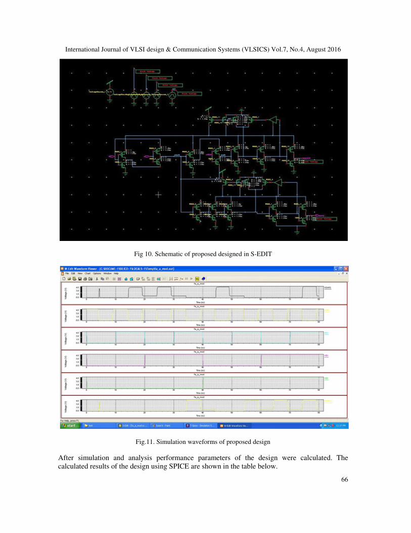
Fig.11. Simulation waveforms of proposed design
After simulation and analysis performance parameters of the design were calculated. The
calculated results of the design using SPICE are shown in the table below.

International Journal of VLSI design & Communication Systems (VLSICS) Vol.7, No.4, August 2016
67
Table 1. Comparison of Results
Parameter\Design Adder1[2] Adder2[2] Adder3 [2] Proposed
Power Consumption (micro-watts) 778.69 micro 933.05 micro 880.58 micro 265.64 micro
Delay SUM (nano-seconds) 2.102 2.591 0.170 0.304
Delay Carry (nano-seconds) 0.866 2.915 0.169 0.158
PDP (Joules) 1.637x10⁻¹²
2.417x10⁻¹²
1.497x10⁻¹³
8.090x10⁻¹⁴
From above table it is clear that the proposed design shows considerable improvement in power
and delay performance, hence PDP in comparison to designs given in [1].
5. CONCLUSIONS
A new technique based on GDI SRL was proposed with advantage of low power consumption to
existing technique. The proposed technique shows two-fold improvement in power consumption
and considerable improvement in delay of the sum and carry outputs. The proposed design can be
used in low power logic circuits due to its low power and low device count.
Further work can be done on improvement of logic levels and of the design and optimization in
terms of number of devices. The proposed technique can also be modified to be used with other
dynamic logic circuits which use input resetting in pre-charge phase.
The other features of the proposed SRLGDI logic are:
1. The signals that propagate through these circuits are pulses. To ensure the correct
operation, it is cascaded with multiple devices.
2. The strict timing constraints observed in pulse mode circuits can be relaxed without
affecting circuit robustness.
3. The data present at evaluation does not require dynamic node to discharge, the precharge
device is not active, hence reducing power.
4. While local generation of the reset assures that the input loading is properly timed and
occurs only when needed, by using a buffered form of the input, it is kept almost as low
as in the normal dynamic logic
5. Minimum delay and fast cycle time are observed when compared to dynamic SRCMOS
logic.
6. Global clock is not required thus it reduces the synchronization problem.
The proposed SRLGDI adder logic performs better than different logic and it’s existing
counterparts. While comparing the four adders, adder1 designed with XOR and MUX presents
low power, less delay and low PDP when compared to adder1 and adder2.Whereas, the proposed
adder presents lowest power among the adders and a very less PDP.On the whole about 66% of
power and 46% of PDP have been achieved using this proposed SRLGDI logic adder when
compared with the best of the existing adders. To fullfill the requirement of monotonicity,
multiple inverters, charge sharing and cascading effects ,delay path inverters and level restoration

International Journal of VLSI design & Communication Systems (VLSICS) Vol.7, No.4, August 2016
68
circuit have been included which slightly increases the total gate count of the circuit and delay,
which is the only con of the proposed SRLGDI logic.
REFERENCES
[1] Uma, R., Dhavachelvan, P., 2012a, New Low power delay element in self resetting logic with
modi.ed gated diffusion input technique. In: IEEE International Conference on Semiconductor
Electronics,
[2] Agrawal, Adarsh Kumar, Wairya, S., Nagaria, R.K., Tiwari, S., 2009. A new mixed gate diffusion
input full adder topology for high speed low power digital circuits. World Appl. Sci. J. 7, 138–144.
[3] Aguirrre-Hernandez, M., Linares-Aranda, M., 2011. CMOS full-adders for energy-efficient
arithmetic applications.IEEETrans.Very Large Scale Integr. VLSI Syst. 19 (4), 718–721.
[4] Balsara, P.T., Steiss, D., 1996. Performance of CMOS differential circuits. IEEE J. Solid-State
Circuits 31, 841–846.
[5] Bisdounis, L.,Gouvetas ,D.,Koufopavlou,O.,1998.Acomparativestudy of CMOS circuit design styles
for low-power high-speed VLSI circuits. Int. J. Electron. 84, 599–613.
[6] Chatzigeorgiou, A., Nikolaidis, S., 2001. Modelling the operation of pass transistor and CPL gates.
Int. J. Electron. 88, 977–1000.
[7] Ghadiry, M.H., Nadisenejani, M., Miryahyaei, M., 2010. A new full swing full adder based on a new
logic approach. World Appl. Sci. 11 (7), 808–812.
[8] Kim, W.J., Kim, Y.B., 2001. A localized self-resetting gate design methodology for low power. In:
Proceedings of the 44th IEEE 2001 Midwest Symposium on Circuits and Systems, August 14–17,
2001, Dayton, OH, pp: 305–308.
[9] Litvin, M.E., Mourad, S., 2005. Self-reset logic for fast arithmetic applications.IEEETrans.VeryLarge
Scale Integr.Syst.13,462–475.
[10] Mirzaee, R.F., Moaiyeri, M.H., Navi, K., 2010. High speed NPCMOS and multi-output dynamic full
adder cells. World Acad. Sci. Eng. Technol. 39, 698–704.
[11] Morgenshtein, A., Fish, A., Wagner, I.A., 2002. Gate-diffusion input (GDI):a power-efficient method
for digital combinatorial circuits. IEEE Trans. VLSI 10, 566–581.
[12] K., K., Kavehei, O., Rouholamini, M., Saha., A., Mehrabi, S., Dadkhahi,N.,2008.Low-powerandhigh-
performance1-BitCMOS full-adder cell. J. Comput. 3 (2), 48–54.
[13] Parameswar, A., Hara, H., Sakurai, T., 1994. A high speed, low power, swingrestoredpass-
transistorlogicbasedmultiplyandaccumulatecircuitformultimediaapplications.In:ProceedingsoftheIEE
ECustomIntegratedCircuitsConference,May1–4,1994,SanDiego,CA,pp:278–281.
[14] Shubin, V.V., 2011. New CMOS circuit implementation of a one bit full adder cell. Russ.
Microlectron. 40 (2), 119–127.
[15] Srivastava, P., Pua, A., Welch, L., 1998. Issues in the design of domino logic circuits. In: Proceedings
of the 8th Great Lakes Symposium on VLSI, February 19–21, 1998, Lafayette, LA, pp: 108–112.

International Journal of VLSI design & Communication Systems (VLSICS) Vol.7, No.4, August 2016
69
[16] Uma, R., 2011. 4-Bit fast adder design: topology and layout with self-resetting logic for low power
VLSI circuits. Int. J. Adv. Eng. Sci. Technol. 7, 197–205.