JFET Frequency Response - Welcome to...
16
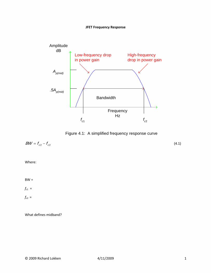
© 2009 Richard Lokken 4/11/2009 1 JFET Frequency Response 2 2 c c BW f f (4.1) Where: BW = f c1 = f c2 = What defines midband? Frequency Hz Amplitude dB A p(mid) .5A p(mid) Bandwidth f c1 f c2 High-frequency drop in power gain Low-frequency drop in power gain Figure 4.1: A simplified frequency response curve
Transcript of JFET Frequency Response - Welcome to...
© 2009 Richard Lokken 4/11/2009 1
JFET Frequency Response
2 2c cBW f f (4.1)
Where:
BW =
fc1 =
fc2 =
What defines midband?
FrequencyHz
AmplitudedB
Ap(mid)
.5Ap(mid)
Bandwidth
fc1 fc2
High-frequencydrop in power gain
Low-frequency dropin power gain
Figure 4.1: A simplified frequency response curve

© 2009 Richard Lokken 4/11/2009 2
The geometric center frequency of the amplifier is _____________________________________.
0 1 2c cf f f (4.2)
Measuring fc1 and fc2
When using the oscilloscope the following procedure is used:
1.
2.
3.
4.
5.
6.
© 2009 Richard Lokken 4/11/2009 3
Graphing the frequency response
1.
2.
3.
Review dB Power Gain
Explain
( ) 10 log outp dB
in
PA
P (4.3)
Convert equation 4.3 to voltage gain.
( )v dBA (4.4)
Low Frequency Response
© 2009 Richard Lokken 4/11/2009 4
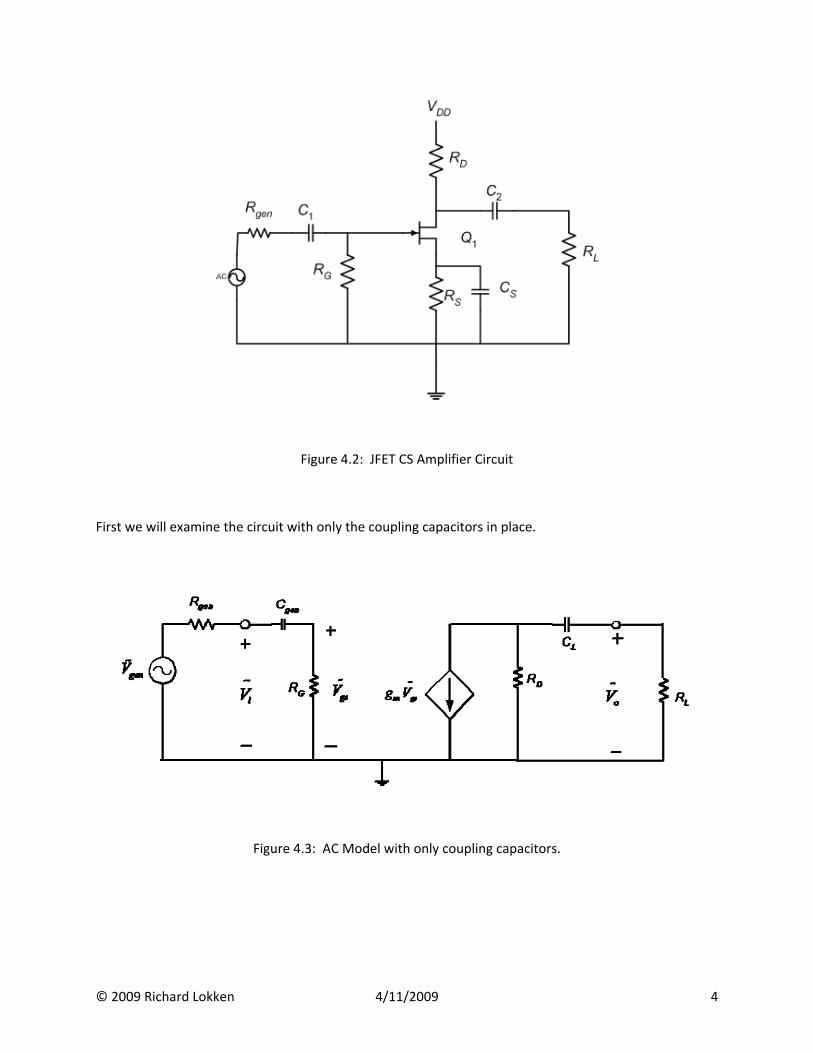
Figure 4.2: JFET CS Amplifier Circuit
First we will examine the circuit with only the coupling capacitors in place.
Figure 4.3: AC Model with only coupling capacitors.
© 2009 Richard Lokken 4/11/2009 5
1
bggen i genR R C
(4.5)
1
bLD L LR R C
(4.6)
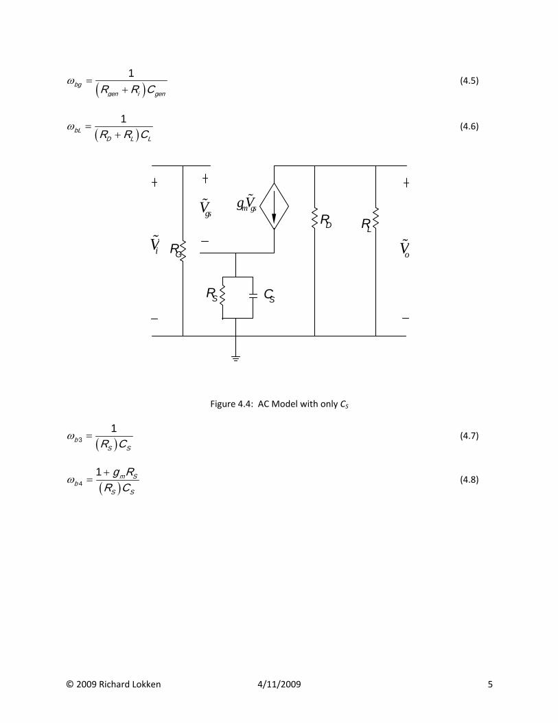
Figure 4.4: AC Model with only CS
3
1b
S SR C (4.7)
4
1 m Sb
S S
g RR C
(4.8)
RG
RD
RS
RL
CS
iV
gsV
oV
m gsgV
© 2009 Richard Lokken 4/11/2009 6
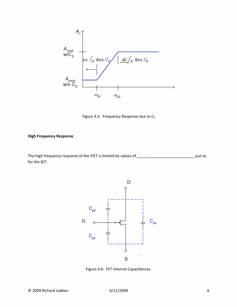
Figure 4.5: Frequency Response due to CS
High Frequency Response
The high frequency response of the JFET is limited by values of ___________________________ just as
for the BJT.
Figure 4.6: FET internal Capacitances.
© 2009 Richard Lokken 4/11/2009 7
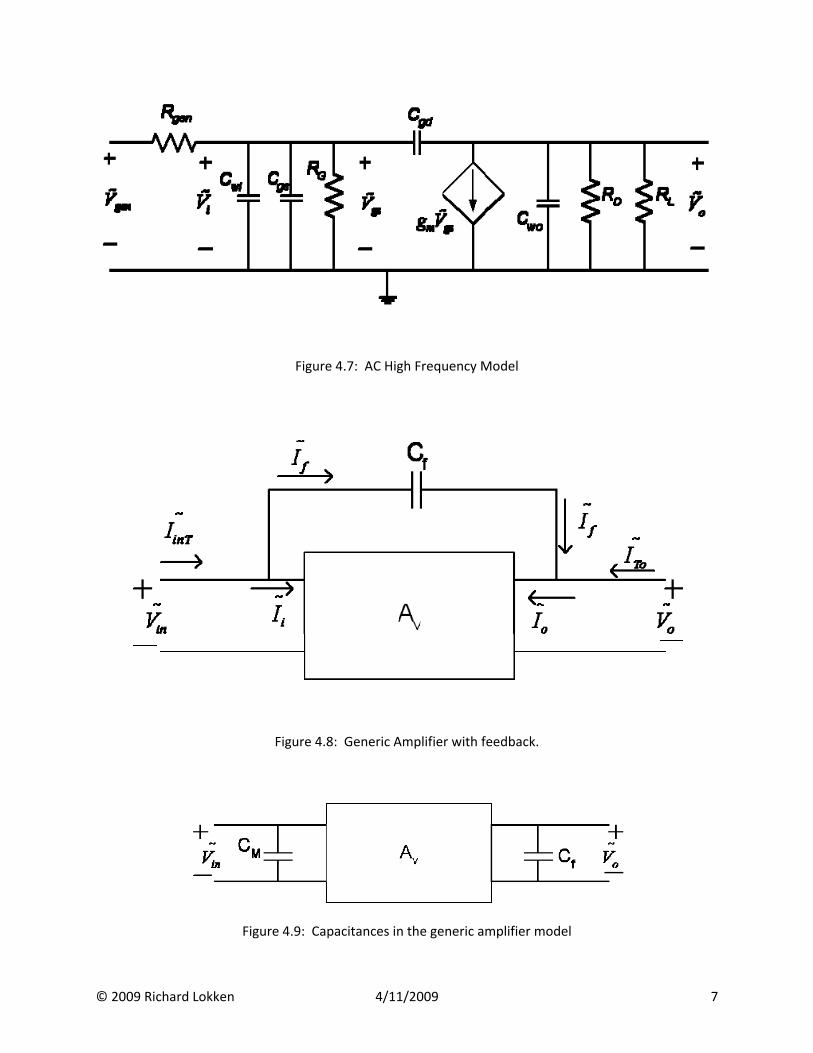
Figure 4.7: AC High Frequency Model
Figure 4.8: Generic Amplifier with feedback.
Figure 4.9: Capacitances in the generic amplifier model
© 2009 Richard Lokken 4/11/2009 8
Write a KCL at the input
inTI (4.9)
1I (4.10)
fI (4.11)
inTI (4.12)
Now Solve for total admittance
inTY (4.13)
inTY (4.14)
By direct comparison of equation 4.13 and equation 4.14
MiC (4.15)
Perform a similar analysis at the output
oTI (4.16)
oI (4.17)
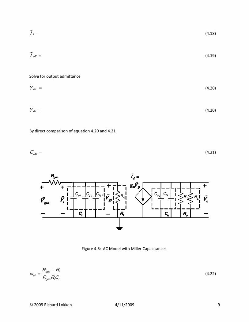
© 2009 Richard Lokken 4/11/2009 9
fI (4.18)
oTI (4.19)
Solve for output admittance
oTY (4.20)
oTY (4.20)
By direct comparison of equation 4.20 and 4.21
MoC (4.21)
Figure 4.6: AC Model with Miller Capacitances.
gen ibi
gen i i
R RR R C
(4.22)
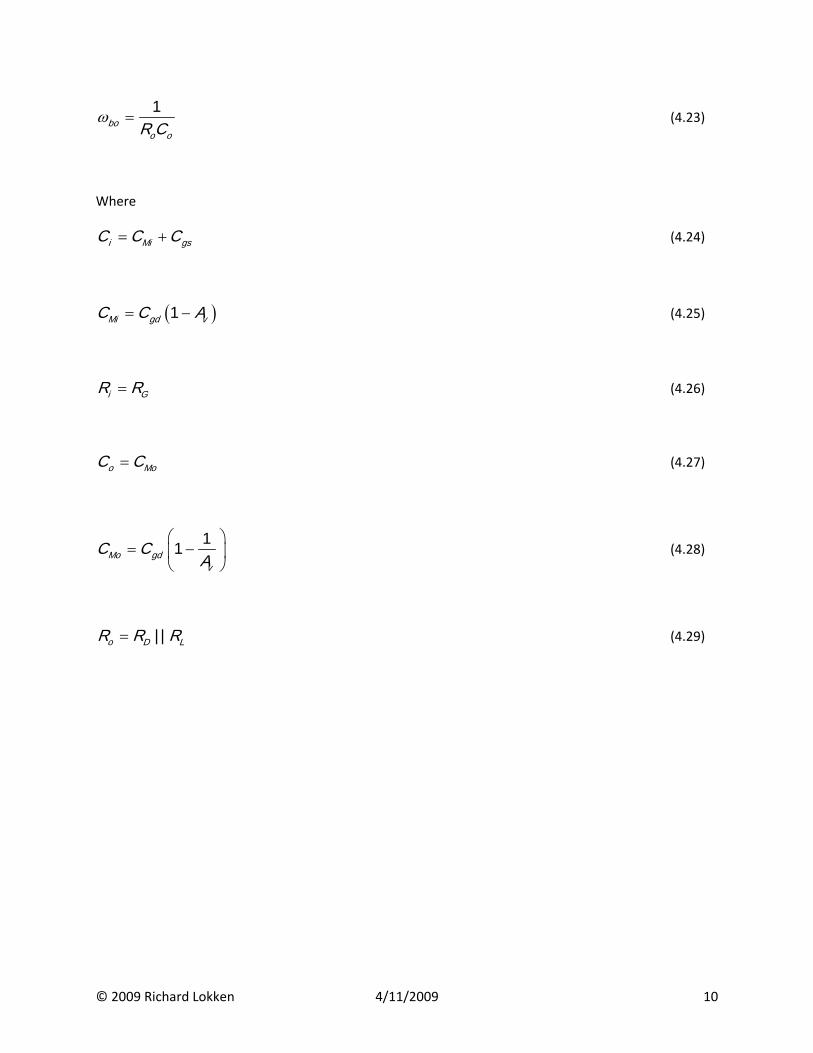
© 2009 Richard Lokken 4/11/2009 10
1bo
o oR C (4.23)
Where
i Mi gsC C C (4.24)
1Mi gd vC C A (4.25)
i GR R (4.26)
o MoC C (4.27)
11Mo gd
v
C CA
(4.28)
||o D LR R R (4.29)
© 2009 Richard Lokken 4/11/2009 11
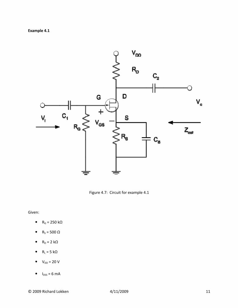
Example 4.1
Figure 4.7: Circuit for example 4.1
Given:
RG = 250 kΩ
RS = 500 Ω
RD = 2 kΩ
RL = 5 kΩ
VDD = 20 V
IDSS = 6 mA
© 2009 Richard Lokken 4/11/2009 12
VP = ‐3 V
C1 = 10 μF
C2 = 10 μF
CS = 100 μF
Cgs = 4 pF
Cgd = 2 pF
Desired:
Mid band Gain
Low Frequency Response
High Frequency Response
Strategy:
Find the Bias Point

© 2009 Richard Lokken 4/11/2009 13
Find the Mid Band Gain
Find the Low Frequency Response
Find the High Frequency Response

© 2009 Richard Lokken 4/11/2009 14
Solution:
Find the Bias Point
Find the Mid Band Gain
Find the Low Frequency Response

© 2009 Richard Lokken 4/11/2009 15
Find the High Frequency Response

© 2009 Richard Lokken 4/11/2009 16