JFET Overview
36
Introduction to FET’s ELEC 121 Author unknown whsmsepiphany4.googlepages.com
-
Upload
m-junaid-sultan -
Category
Documents
-
view
140 -
download
8
Transcript of JFET Overview
Introduction to FET’s
ELEC 121Author unknown
whsmsepiphany4.googlepages.com
ELEC 121 2January 2004
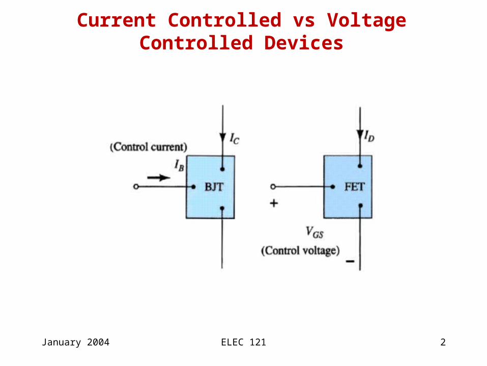
Current Controlled vs Voltage Controlled Devices
ELEC 121 3January 2004
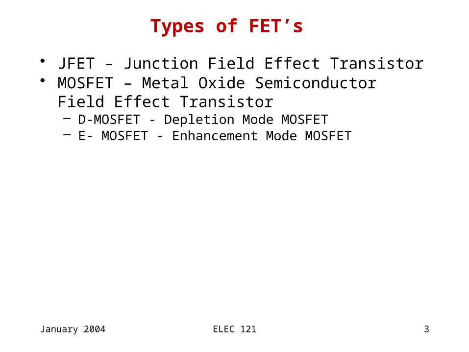
• JFET – Junction Field Effect Transistor• MOSFET – Metal Oxide Semiconductor Field Effect
Transistor– D-MOSFET - Depletion Mode MOSFET– E- MOSFET - Enhancement Mode MOSFET
Types of FET’s
ELEC 121 4January 2004
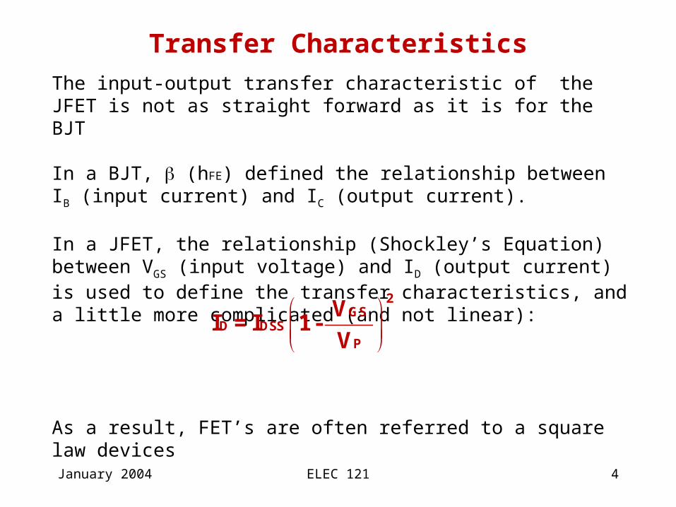
Transfer Characteristics
The input-output transfer characteristic of the JFET is not as straight forward as it is for the BJT
In a BJT, (hFE) defined the relationship between IB (input current) and IC (output current).
In a JFET, the relationship (Shockley’s Equation) between VGS (input voltage) and ID (output current) is used to define the transfer characteristics, and a little more complicated (and not linear):
As a result, FET’s are often referred to a square law devices
2GS
D DSSP
V I = I 1 -
V

ELEC 121 5January 2004
JFET ConstructionThere are two types of JFET’s: n-channel and p-channel.
The n-channel is more widely used.
There are three terminals: Drain (D) and Source (S) are connected to n-channelGate (G) is connected to the p-type material
ELEC 121 6January 2004
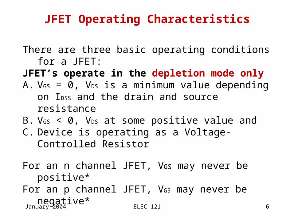
JFET Operating Characteristics
There are three basic operating conditions for a JFET:JFET’s operate in the depletion mode onlyA. VGS = 0, VDS is a minimum value depending on IDSS and the
drain and source resistanceB. VGS < 0, VDS at some positive value andC. Device is operating as a Voltage-Controlled Resistor
For an n channel JFET, VGS may never be positive*For an p channel JFET, VGS may never be negative*
ELEC 121 7January 2004
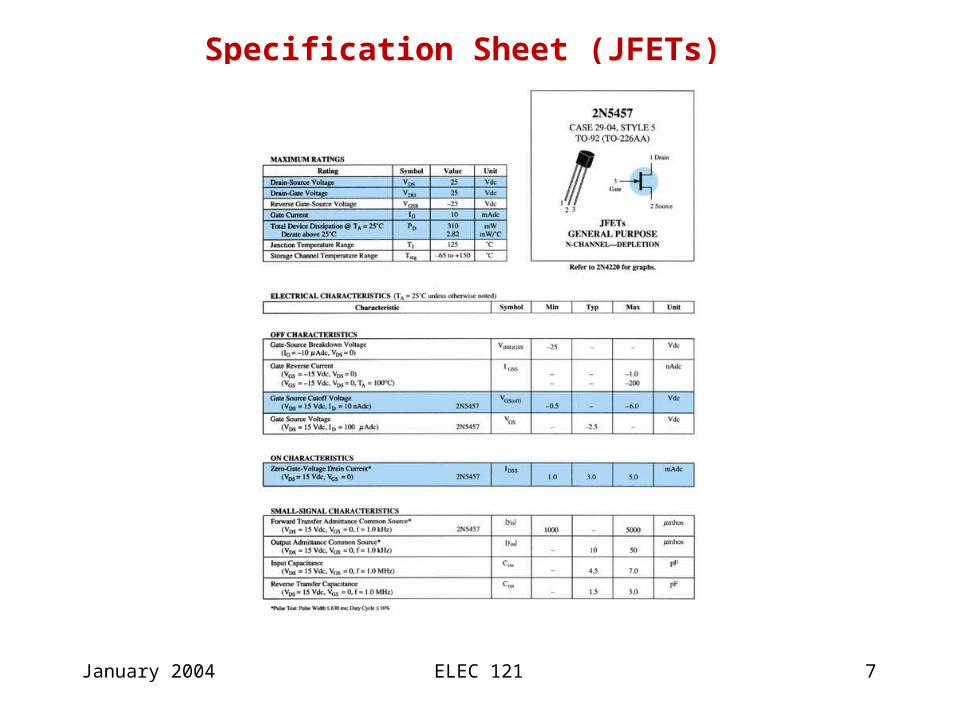
Specification Sheet (JFETs)
ELEC 121 8January 2004
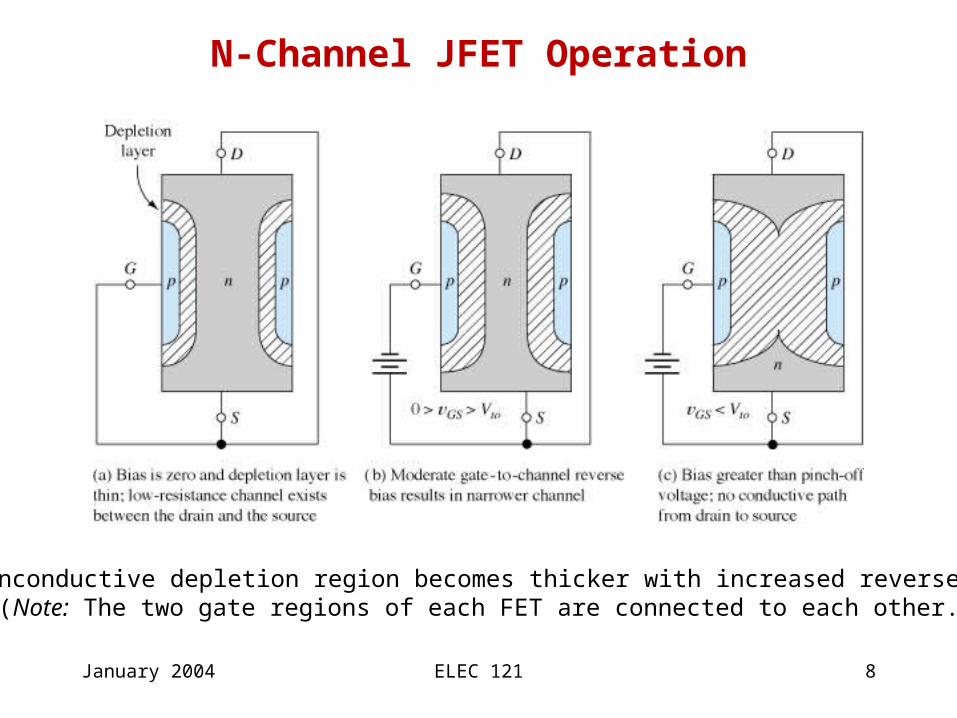
The nonconductive depletion region becomes thicker with increased reverse bias. (Note: The two gate regions of each FET are connected to each other.)
N-Channel JFET Operation

ELEC 121 9January 2004
N-Channel JFET Symbol
ELEC 121 10January 2004
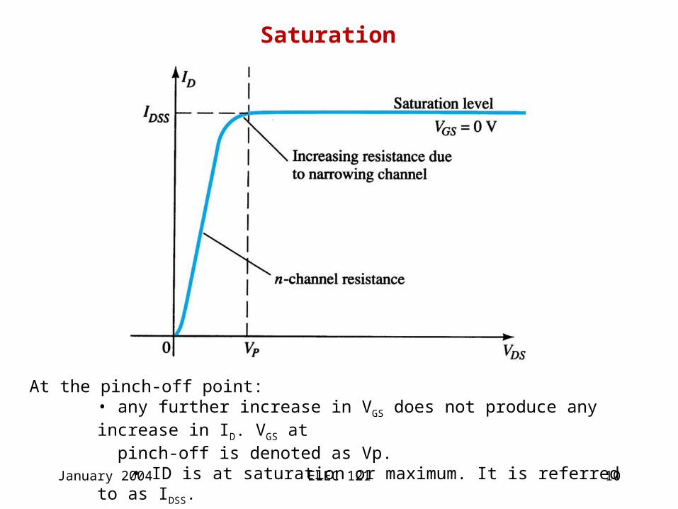
Saturation
At the pinch-off point: • any further increase in VGS does not produce any increase in ID. VGS at pinch-off is denoted as Vp.
• ID is at saturation or maximum. It is referred to as IDSS. • The ohmic value of the channel is at maximum.
ELEC 121 11January 2004
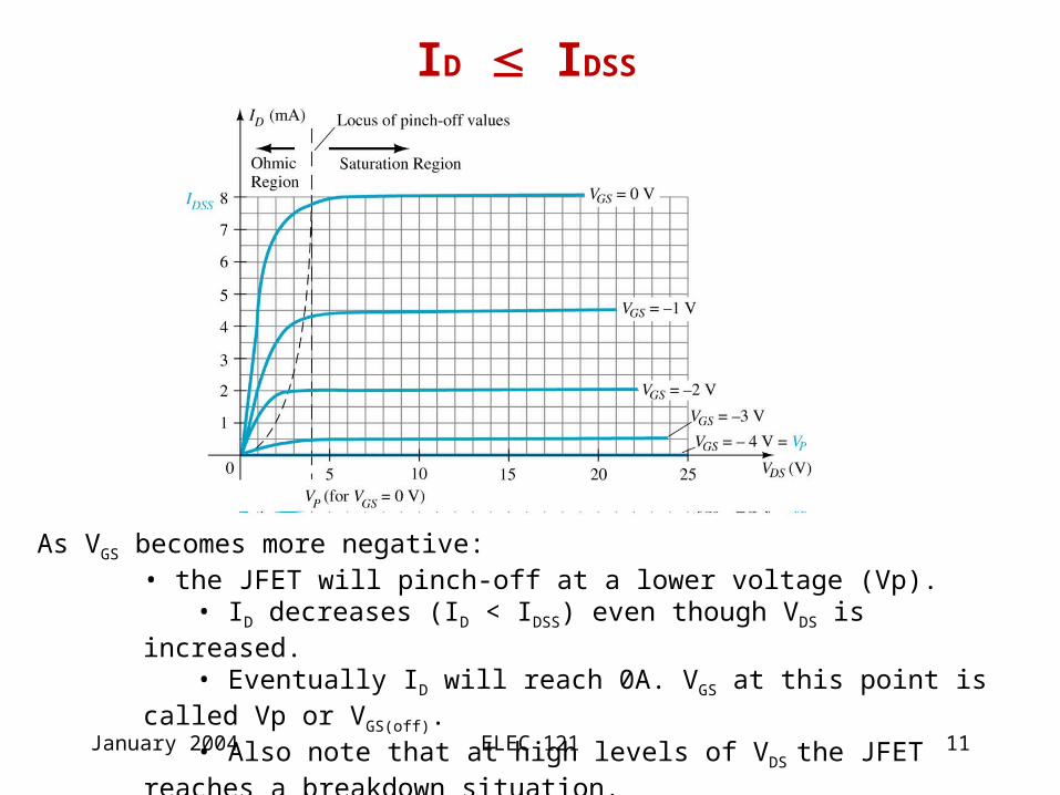
ID IDSS
As VGS becomes more negative:• the JFET will pinch-off at a lower voltage (Vp).
• ID decreases (ID < IDSS) even though VDS is increased.• Eventually ID will reach 0A. VGS at this point is called Vp or VGS(off).• Also note that at high levels of VDS the JFET reaches a breakdown
situation. ID will increases uncontrollably if VDS > VDSmax.
ELEC 121 12January 2004
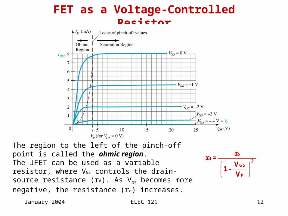
FET as a Voltage-Controlled Resistor
The region to the left of the pinch-off point is called the ohmic region.The JFET can be used as a variable resistor, where VGS controls the drain-source resistance (rd). As VGS becomes more negative, the resistance (rd) increases.
od 2
GS
P
r r =
V 1 -
V
ELEC 121 13January 2004
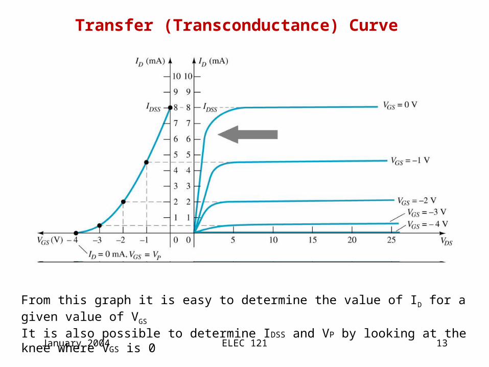
Transfer (Transconductance) Curve
From this graph it is easy to determine the value of ID for a given value of VGS
It is also possible to determine IDSS and VP by looking at the knee where VGS is 0
ELEC 121 14January 2004
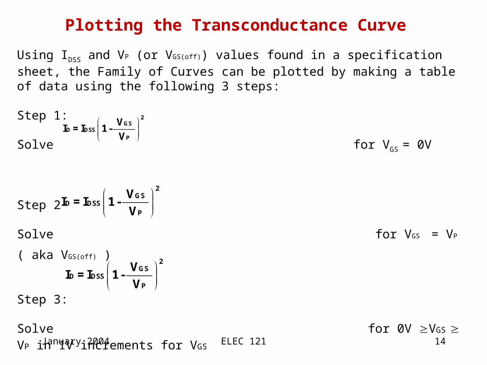
Plotting the Transconductance Curve
Using IDSS and VP (or VGS(off)) values found in a specification sheet, the Family of Curves can be plotted by making a table of data using the following 3 steps:
Step 1:
Solve for VGS = 0V
Step 2
Solve for VGS = VP ( aka VGS(off) )
Step 3:
Solve for 0V VGS VP in 1V increments for VGS
2GS
D DSSP
V I = I 1 -
V
2GS
D DSSP
V I = I 1 -
V
2GS
D DSSP
V I = I 1 -
V
ELEC 121 15January 2004
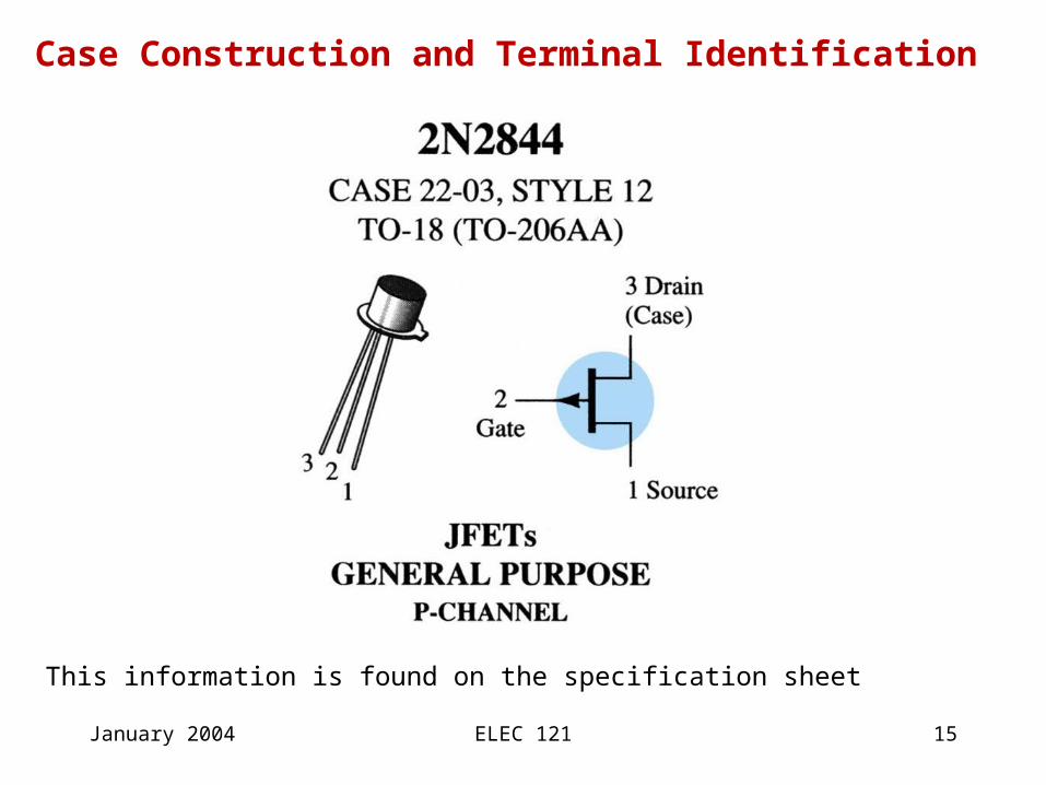
Case Construction and Terminal Identification
This information is found on the specification sheet
ELEC 121 16January 2004
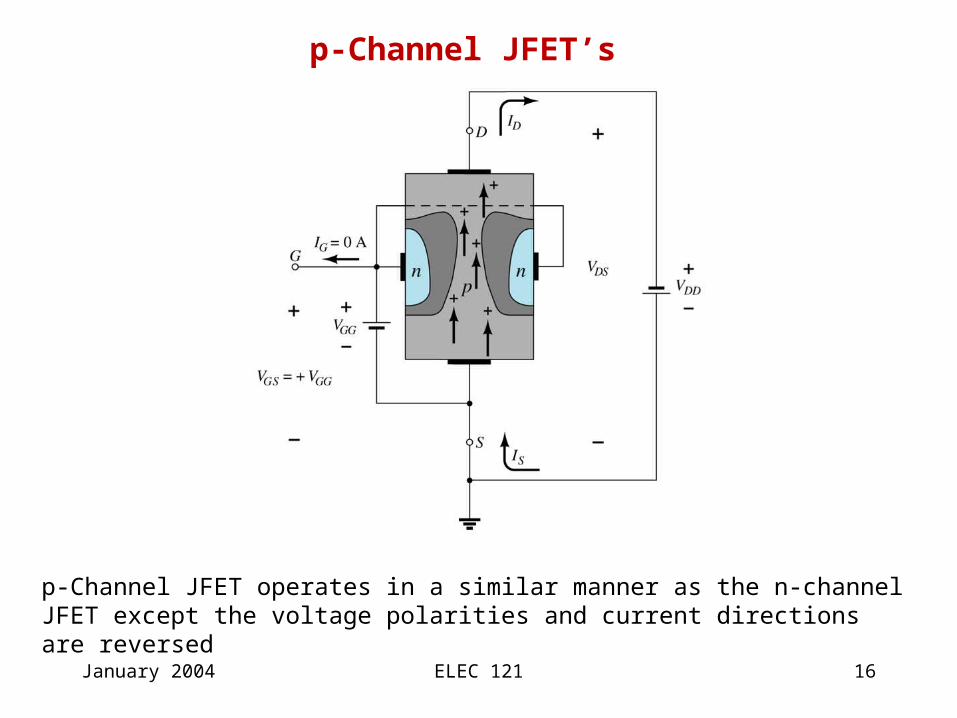
p-Channel JFET’s
p-Channel JFET operates in a similar manner as the n-channel JFET except the voltage polarities and current directions are reversed
ELEC 121 17January 2004
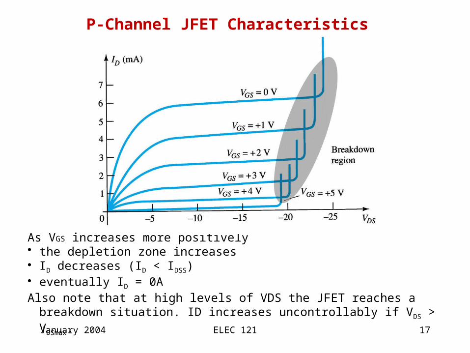
P-Channel JFET Characteristics
As VGS increases more positively• the depletion zone increases• ID decreases (ID < IDSS)• eventually ID = 0AAlso note that at high levels of VDS the JFET reaches a breakdown situation. ID
increases uncontrollably if VDS > VDSmax.

MOSFET’s
ELEC 121 19January 2004
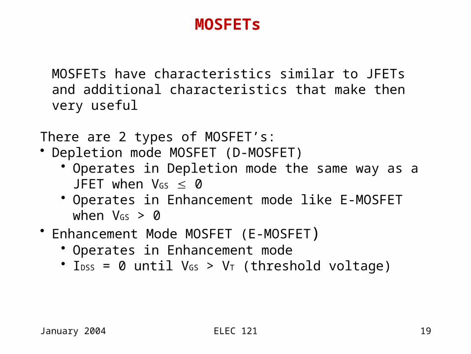
MOSFETs
MOSFETs have characteristics similar to JFETs and additional characteristics that make then very useful
There are 2 types of MOSFET’s:• Depletion mode MOSFET (D-MOSFET)
• Operates in Depletion mode the same way as a JFET when VGS 0• Operates in Enhancement mode like E-MOSFET when VGS > 0
• Enhancement Mode MOSFET (E-MOSFET)• Operates in Enhancement mode• IDSS = 0 until VGS > VT (threshold voltage)
ELEC 121 20January 2004
MOSFET Handling
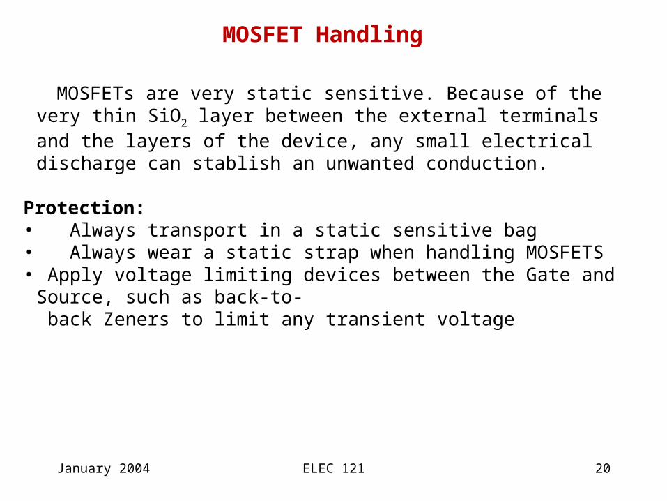
MOSFETs are very static sensitive. Because of the very thin SiO2 layer between the external terminals and the layers of the device, any small electrical discharge can stablish an unwanted conduction.
Protection:• Always transport in a static sensitive bag• Always wear a static strap when handling MOSFETS• Apply voltage limiting devices between the Gate and Source, such as back-to-
back Zeners to limit any transient voltage
ELEC 121 21January 2004
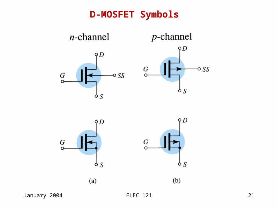
D-MOSFET Symbols
ELEC 121 22January 2004
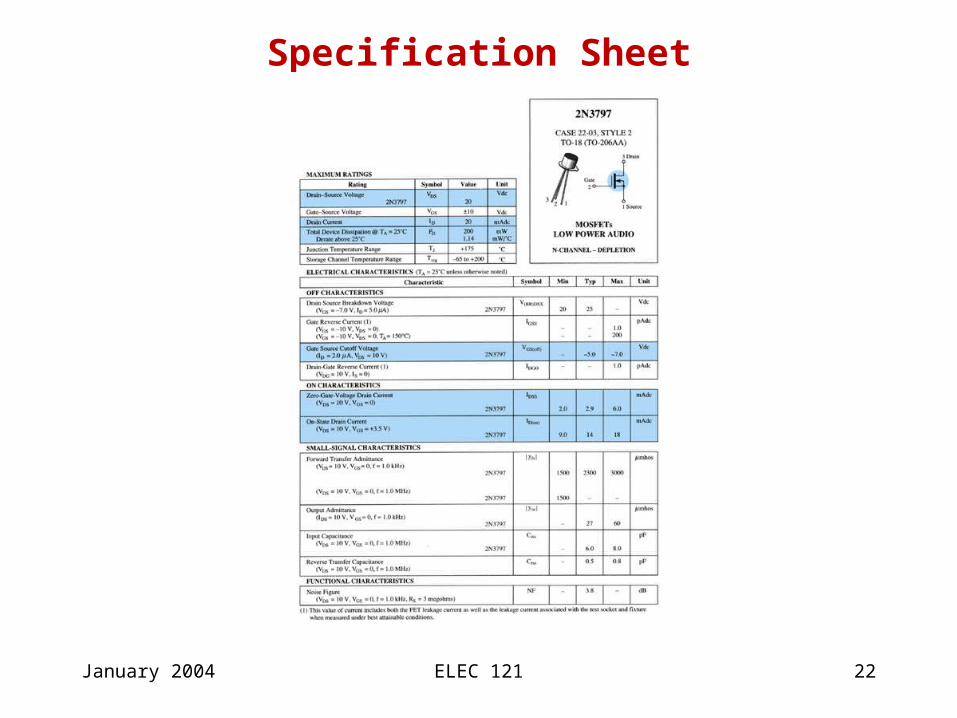
Specification Sheet

ELEC 121 23January 2004
Depletion Mode MOSFET Construction
The Drain (D) and Source (S) leads connect to the to n-doped regionsThese N-doped regions are connected via an n-channelThis n-channel is connected to the Gate (G) via a thin insulating layer of SiO2
The n-doped material lies on a p-doped substrate that may have an additional terminal connection called SS
ELEC 121 24January 2004
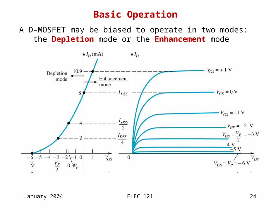
Basic Operation
A D-MOSFET may be biased to operate in two modes: the Depletion mode or the Enhancement mode
ELEC 121 25January 2004
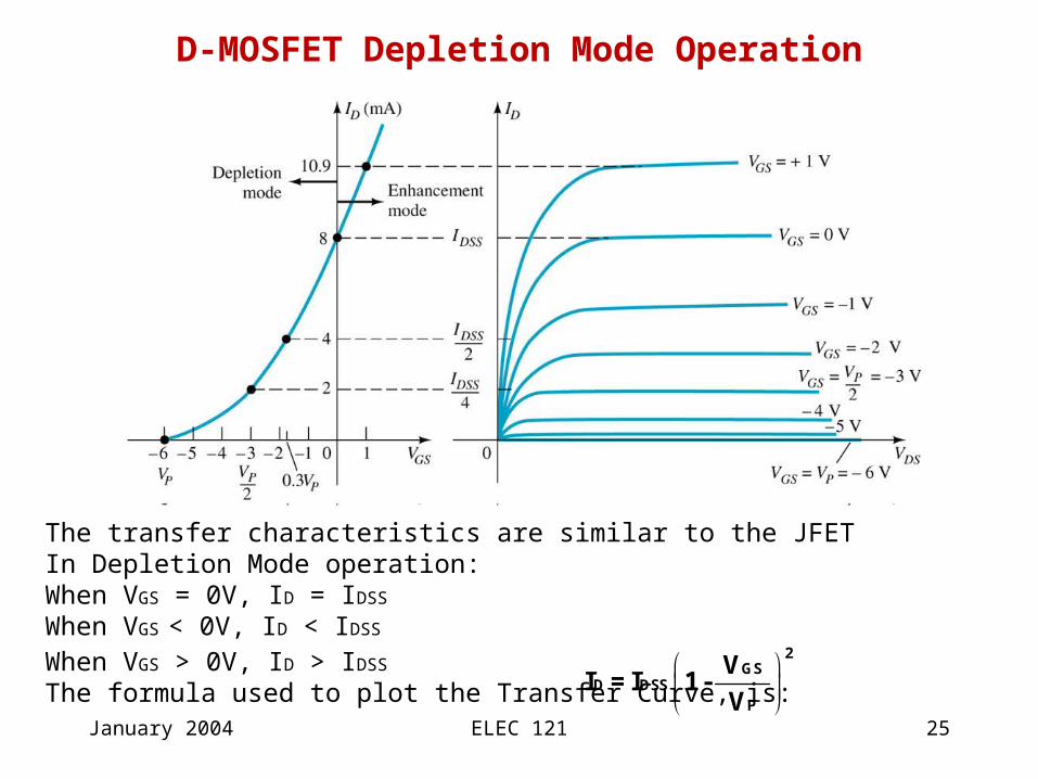
D-MOSFET Depletion Mode Operation
The transfer characteristics are similar to the JFETIn Depletion Mode operation:When VGS = 0V, ID = IDSS
When VGS < 0V, ID < IDSS
When VGS > 0V, ID > IDSS
The formula used to plot the Transfer Curve, is:
2GS
D DSSP
V I = I 1 -
V
ELEC 121 26January 2004
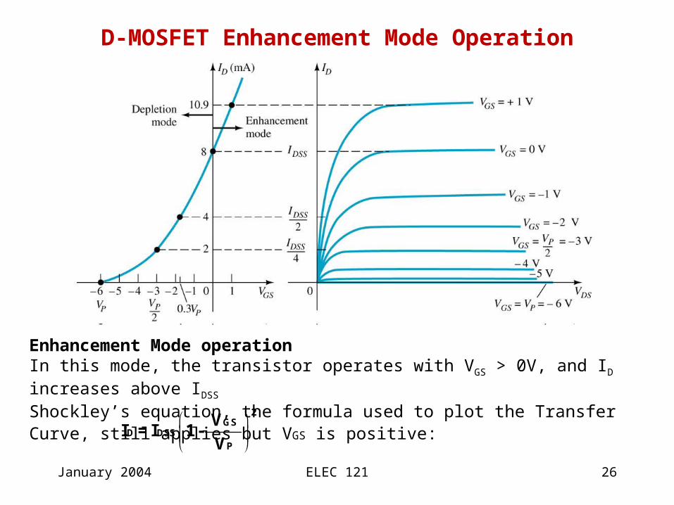
D-MOSFET Enhancement Mode Operation
Enhancement Mode operationIn this mode, the transistor operates with VGS > 0V, and ID increases above IDSS
Shockley’s equation, the formula used to plot the Transfer Curve, still applies but VGS is positive:
2GS
D DSSP
V I = I 1 -
V
ELEC 121 27January 2004
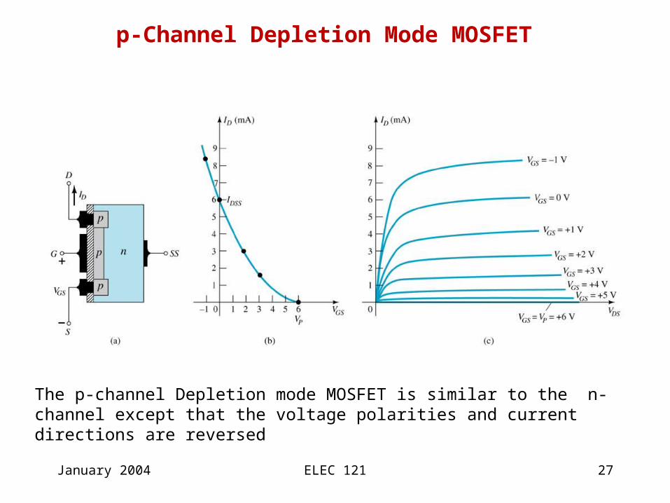
p-Channel Depletion Mode MOSFET
The p-channel Depletion mode MOSFET is similar to the n-channel except that the voltage polarities and current directions are reversed

Enhancement ModeMOSFET’s
ELEC 121 29January 2004
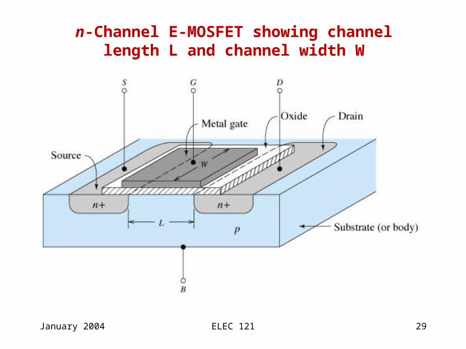
n-Channel E-MOSFET showing channel length L and channel width W
ELEC 121 30January 2004
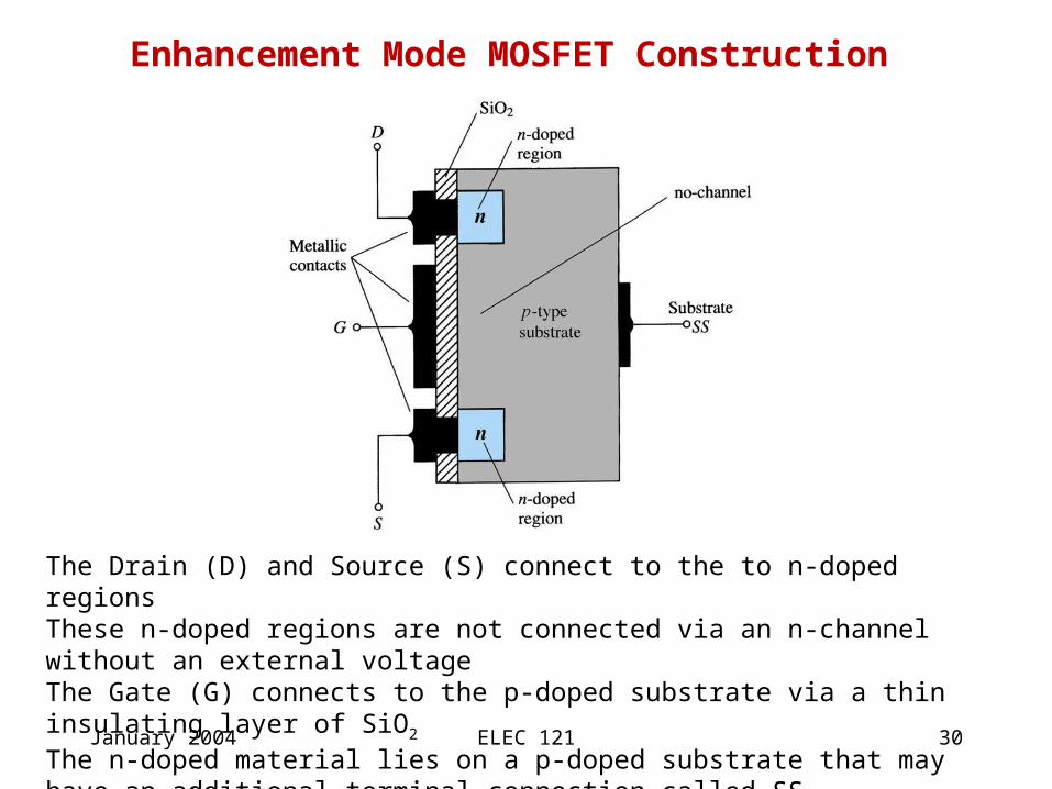
Enhancement Mode MOSFET Construction
The Drain (D) and Source (S) connect to the to n-doped regionsThese n-doped regions are not connected via an n-channel without an external voltageThe Gate (G) connects to the p-doped substrate via a thin insulating layer of SiO2
The n-doped material lies on a p-doped substrate that may have an additional terminal connection called SS
ELEC 121 31January 2004
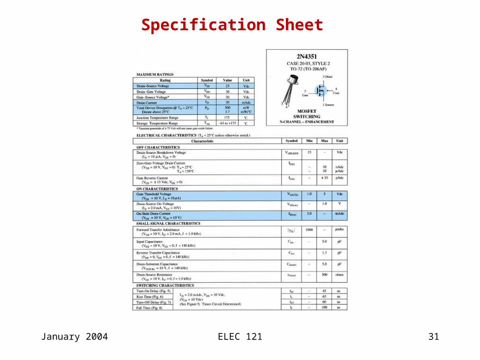
Specification Sheet
ELEC 121 32January 2004
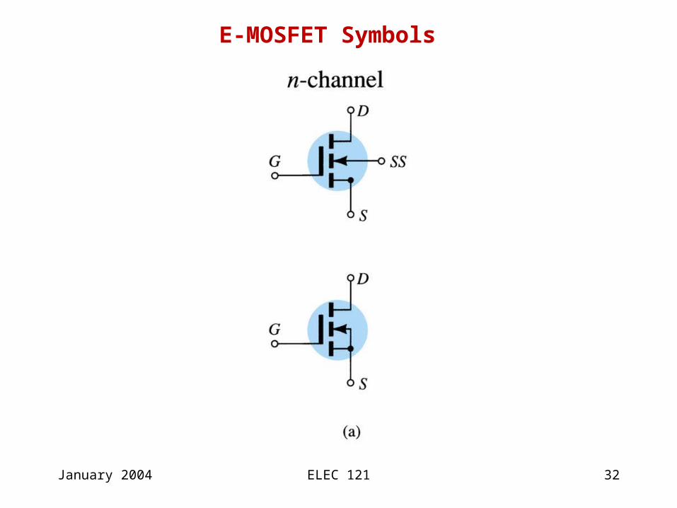
E-MOSFET Symbols
ELEC 121 33January 2004
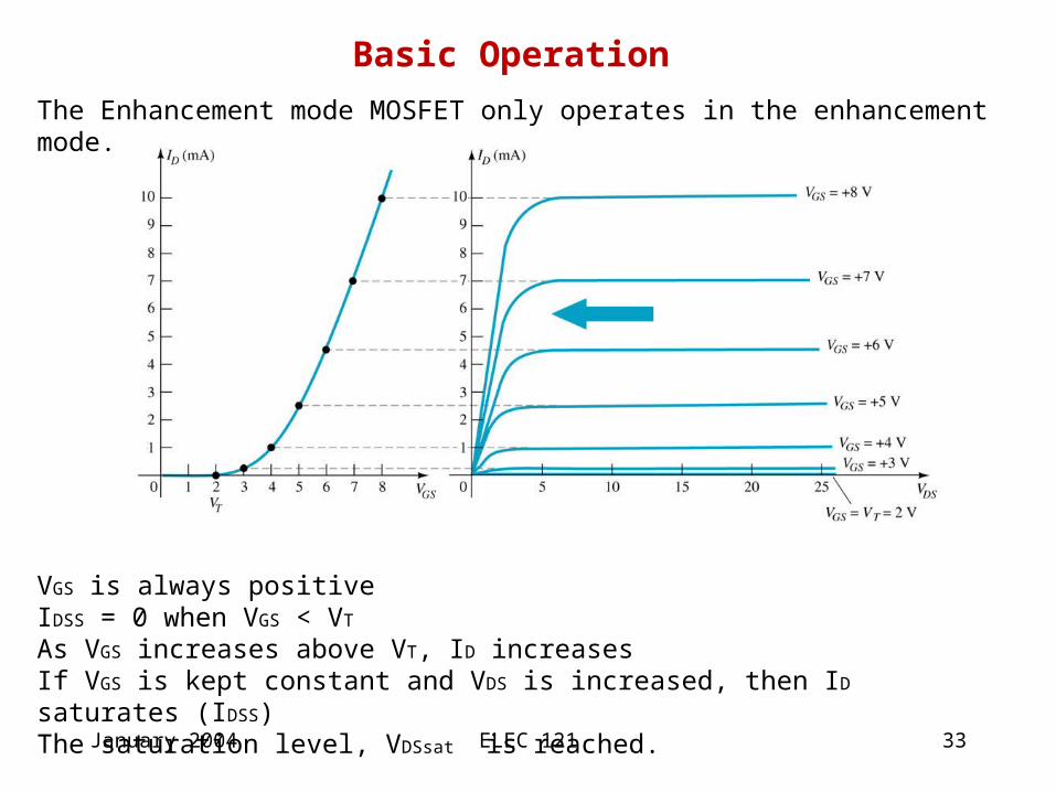
Basic Operation
The Enhancement mode MOSFET only operates in the enhancement mode.
VGS is always positiveIDSS = 0 when VGS < VT
As VGS increases above VT, ID increasesIf VGS is kept constant and VDS is increased, then ID saturates (IDSS)The saturation level, VDSsat is reached.
ELEC 121 34January 2004
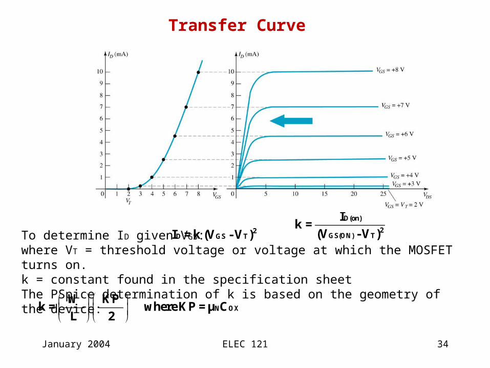
Transfer Curve
To determine ID given VGS:where VT = threshold voltage or voltage at which the MOSFET turns on.k = constant found in the specification sheetThe PSpice determination of k is based on the geometry of the device:
2D GS TI = k (V - V )
D(on)
2GS(ON) T
Ik =
(V - V )
N OX W KP
k = where KP = μ C L 2
ELEC 121 35January 2004
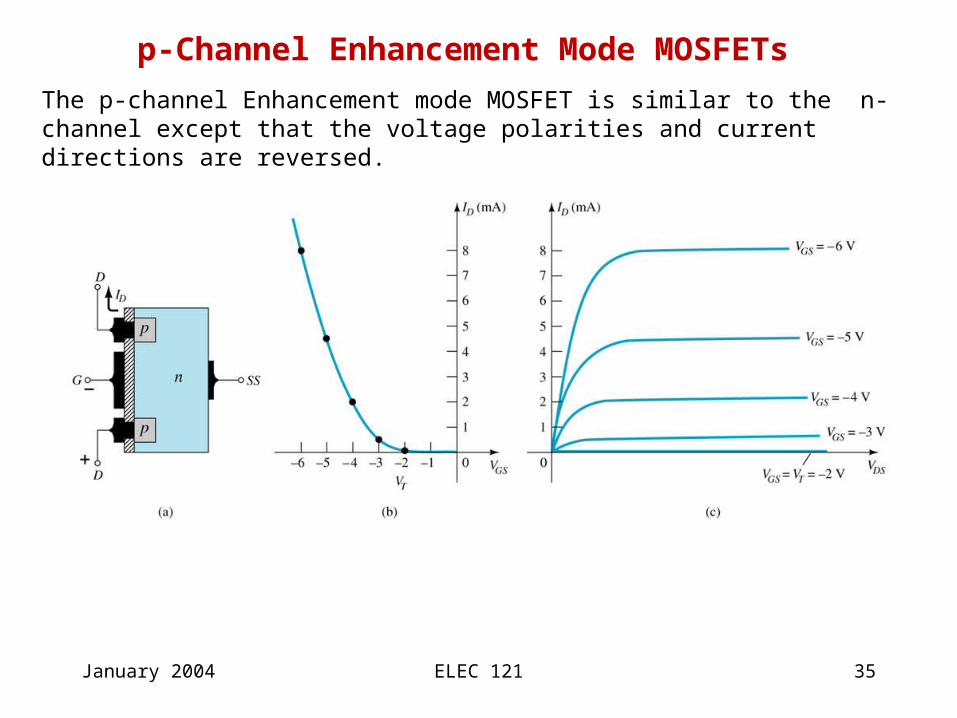
p-Channel Enhancement Mode MOSFETs
The p-channel Enhancement mode MOSFET is similar to the n-channel except that the voltage polarities and current directions are reversed.
ELEC 121 36January 2004
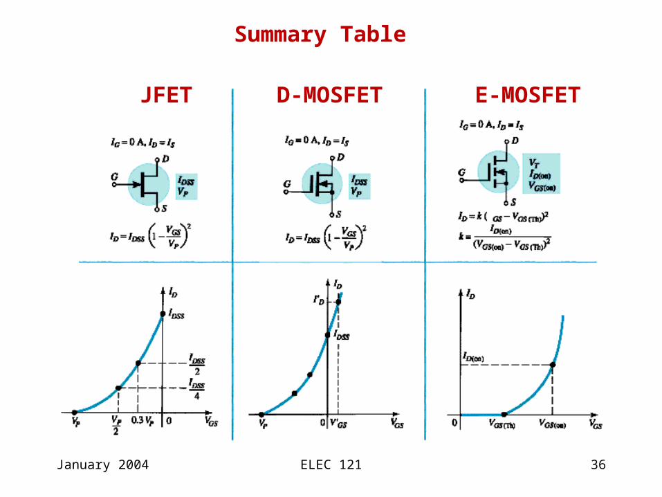
Summary Table
JFET D-MOSFET E-MOSFET