JFET AND ITS CHARACTERISTICS · P a g e | 1 Unit 6| Field Effect Transistor (FET) And MOSFET 3rd...
25
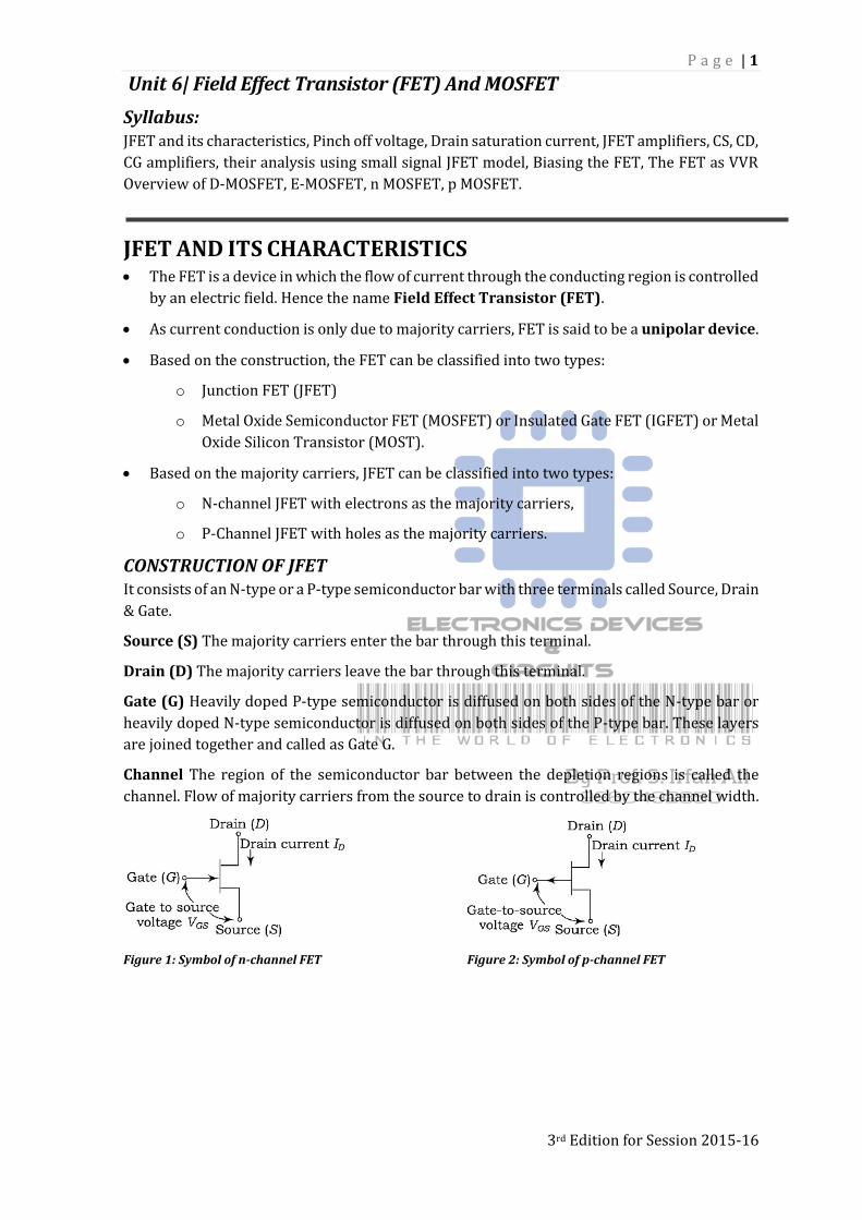
Page | 1 Unit 6| Field Effect Transistor (FET) And MOSFET 3 rd Edition for Session 2015-16 Syllabus: JFET and its characteristics, Pinch off voltage, Drain saturation current, JFET amplifiers, CS, CD, CG amplifiers, their analysis using small signal JFET model, Biasing the FET, The FET as VVR Overview of D-MOSFET, E-MOSFET, n MOSFET, p MOSFET. JFET AND ITS CHARACTERISTICS The FET is a device in which the flow of current through the conducting region is controlled by an electric field. Hence the name Field Effect Transistor (FET). As current conduction is only due to majority carriers, FET is said to be a unipolar device. Based on the construction, the FET can be classified into two types: o Junction FET (JFET) o Metal Oxide Semiconductor FET (MOSFET) or Insulated Gate FET (IGFET) or Metal Oxide Silicon Transistor (MOST). Based on the majority carriers, JFET can be classified into two types: o N-channel JFET with electrons as the majority carriers, o P-Channel JFET with holes as the majority carriers. CONSTRUCTION OF JFET It consists of an N-type or a P-type semiconductor bar with three terminals called Source, Drain & Gate. Source (S) The majority carriers enter the bar through this terminal. Drain (D) The majority carriers leave the bar through this terminal. Gate (G) Heavily doped P-type semiconductor is diffused on both sides of the N-type bar or heavily doped N-type semiconductor is diffused on both sides of the P-type bar. These layers are joined together and called as Gate G. Channel The region of the semiconductor bar between the depletion regions is called the channel. Flow of majority carriers from the source to drain is controlled by the channel width. Figure 1: Symbol of n-channel FET Figure 2: Symbol of p-channel FET
Transcript of JFET AND ITS CHARACTERISTICS · P a g e | 1 Unit 6| Field Effect Transistor (FET) And MOSFET 3rd...
P a g e | 1
Unit 6| Field Effect Transistor (FET) And MOSFET
3rd Edition for Session 2015-16
Syllabus: JFET and its characteristics, Pinch off voltage, Drain saturation current, JFET amplifiers, CS, CD,
CG amplifiers, their analysis using small signal JFET model, Biasing the FET, The FET as VVR
Overview of D-MOSFET, E-MOSFET, n MOSFET, p MOSFET.
JFET AND ITS CHARACTERISTICS The FET is a device in which the flow of current through the conducting region is controlled
by an electric field. Hence the name Field Effect Transistor (FET).
As current conduction is only due to majority carriers, FET is said to be a unipolar device.
Based on the construction, the FET can be classified into two types:
o Junction FET (JFET)
o Metal Oxide Semiconductor FET (MOSFET) or Insulated Gate FET (IGFET) or Metal
Oxide Silicon Transistor (MOST).
Based on the majority carriers, JFET can be classified into two types:
o N-channel JFET with electrons as the majority carriers,
o P-Channel JFET with holes as the majority carriers.
CONSTRUCTION OF JFET It consists of an N-type or a P-type semiconductor bar with three terminals called Source, Drain
& Gate.
Source (S) The majority carriers enter the bar through this terminal.
Drain (D) The majority carriers leave the bar through this terminal.
Gate (G) Heavily doped P-type semiconductor is diffused on both sides of the N-type bar or
heavily doped N-type semiconductor is diffused on both sides of the P-type bar. These layers
are joined together and called as Gate G.
Channel The region of the semiconductor bar between the depletion regions is called the
channel. Flow of majority carriers from the source to drain is controlled by the channel width.
Figure 1: Symbol of n-channel FET
Figure 2: Symbol of p-channel FET
P a g e | 2
Unit 6| Field Effect Transistor (FET) And MOSFET
3rd Edition for Session 2015-16
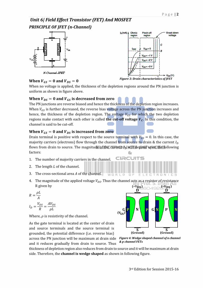
Figure 3: Drain characteristics of JFET
PRINCIPLE OF JFET (n-Channel)
When 𝑽𝑮𝑺 = 𝟎 and 𝑽𝑫𝑺 = 𝟎
When no voltage is applied, the thickness of the depletion regions around the PN junction is
uniform as shown in figure above.
When 𝑽𝑫𝑺 = 𝟎 and 𝑽𝑮𝑺 is decreased from zero
The PN junctions are reverse biased and hence the thickness of the depletion region increases.
When 𝑉𝐺𝑆 is further decreased, the reverse bias voltage across the PN junction increases and
hence, the thickness of the depletion region. The voltage 𝑉𝐺𝑆 for which the two depletion
regions make contact with each other is called the cut-off voltage 𝑽𝑪. In this condition, the
channel is said to be cut-off.
When 𝑽𝑮𝑺 = 𝟎 and 𝑽𝑫𝑺 is increased from zero
Drain terminal is positive with respect to the source terminal with 𝑉𝐺𝑆 = 0. In this case, the
majority carriers (electrons) flow through the channel from source to drain & the current 𝐼𝐷
flows from drain to source. The magnitude of the current 𝐼𝐷 will depend upon the following
factors:
1. The number of majority carriers in the channel.
2. The length 𝐿 of the channel.
3. The cross-sectional area 𝐴 of the channel.
4. The magnitude of the applied voltage 𝑉𝐷𝑆. Thus the channel acts as a resistor of resistance
R given by
𝑅 =𝜌𝐿
𝐴
𝐼𝐷 =𝑉𝐷𝑆
𝑅=
𝐴𝑉𝐷𝑆
𝜌𝐿
Where, 𝜌 is resistivity of the channel.
As the gate terminal is located at the center of drain
and source terminals and the source terminal is
grounded, the potential difference (i.e. reverse bias)
across the PN junction will be maximum at drain side
and it reduces gradually from drain to source. Thus
thickness of depletion region also reduces from drain to source and it will be maximum at drain
side. Therefore, the channel is wedge shaped as shown in following figure.
Figure 4: Wedge shaped channel of n channel & p channel FETs
P a g e | 3
Unit 6| Field Effect Transistor (FET) And MOSFET
3rd Edition for Session 2015-16
As 𝑉𝐷𝑆 is increased, the cross-sectional area of the channel will be reduced. At a certain value
𝑉𝐷𝑆 of the channel cross-sectional area becomes zero. At this voltage, the channel is said to be
pinched off and the drain voltage is called the pinch-off voltage 𝑽𝑷.
When 𝑽𝑮𝑺 is negative and 𝑽𝑫𝑺 is increased
For negative 𝑉𝐺𝑆, the curve 𝐼𝐷 versus 𝑉𝐷𝑆 is similar to previous case when 𝑉𝐺𝑆 = 0𝑉, but the
values of 𝑉𝑃 and 𝑽𝑫𝑩𝑹(Drain Break down Voltage) are lower1 as shown in figure above.
DRAIN CHARACTERISTICS 1. As 𝑉𝐷𝑆 is increased from zero, 𝐼𝐷 increases
along 𝑂𝑃, and the rate of increase of 𝐼𝐷 with
𝑉𝐷𝑆 decreases as shown in figure above. The
region from 𝑉𝐷𝑆 = 0𝑉 to 𝑉𝐷𝑆 = 𝑉𝑃 is called
the ohmic region. In the ohmic region of
channel, the drain to source resistance
𝑉𝐷𝑆/𝐼𝐷 is related to the gate voltage 𝑉𝐺𝑆 in a
linear manner. Because of gate controlled
linear nature, it is also called as a voltage
variable resistor (VVR) or voltage
dependent resistor (VDR).
2. When 𝑉𝐷𝑆 = 𝑉𝑃, 𝐼𝐷 becomes maximum. When 𝑉𝐷𝑆 is increased beyond 𝑉𝑃, the length of the
pinch-off or saturation region increases. Hence, there is no further increase of 𝐼𝐷.
3. At a certain voltage corresponding to the point 𝐵, 𝐼𝐷 suddenly increases. This effect is due
to the Avalanche multiplication of electrons caused by breaking of covalent bonds of silicon
atoms in the depletion region between the gate and the drain. The drain voltage at which
the breakdown occurs is denoted by 𝑉𝐷𝐵𝑅. The variation of 𝐼𝐷 with 𝑉𝐷𝑆 when 𝑉𝐺𝑆 = 0 is
shown in figure above by the curve OPBC.
CHARACTERISTICS PARAMETERS OF JFET In a JFET, the drain current 𝐼𝐷 depends upon the drain voltage 𝑉𝐷𝑆 and the gate voltage 𝑉𝐺𝑆.
Any one of these variables may be fixed to get the relation between the other two. These
relations are defined by the three parameters:
Mutual conductance or transconductance, 𝒈𝒎
It is defined as the ratio of a fractional change in the drain current to the fractional change in
the gate voltage at a constant drain voltage. The change in 𝐼𝐷 and 𝑉𝐺𝑆 should be considered on
the linear part of the transfer characteristics. It is measured in the unit of mho. It is given by,
𝑔𝑚 = (𝜕𝐼𝐷
𝜕𝑉𝐺𝑆)
𝑉𝐷𝑆
=Δ𝐼𝐷
Δ𝑉𝐺𝑆, 𝑤𝑖𝑡ℎ 𝑉𝐷𝑆 𝑐𝑜𝑛𝑠𝑡𝑎𝑛𝑡
Drain resistance, 𝒓𝒅
It is defined as the ratio of a fractional change in the drain voltage to the fractional change in
the drain current at a constant gate voltage. It is measured in the unit of ohms (Ω). It is given
by,
1 Cutoff state will be attained at smaller value of VGS
Figure 5: Drain characteristics of JFET
P a g e | 4
Unit 6| Field Effect Transistor (FET) And MOSFET
3rd Edition for Session 2015-16
𝑟𝑑 = (𝜕𝑉𝐷𝑆
𝜕𝐼𝐷)
𝑉𝐺𝑆
=Δ𝑉𝐷𝑆
Δ𝐼𝐷, 𝑤𝑖𝑡ℎ 𝑉𝐺𝑆 𝑐𝑜𝑛𝑠𝑡𝑎𝑛𝑡
Drain conductance, 𝒈𝒅
It is reciprocal of 𝑟𝑑 and is defined as the ratio of a fractional change in the drain current to the
fractional change in the drain voltage at a constant gate voltage. It is measured in the unit of
mho (Ω−1). It is given by,
𝑔𝑑 = (𝜕𝐼𝐷
𝜕𝑉𝐷𝑆)
𝑉𝐺𝑆
=Δ𝐼𝐷
Δ𝑉𝐷𝑆, 𝑤𝑖𝑡ℎ 𝑉𝐺𝑆 𝑐𝑜𝑛𝑠𝑡𝑎𝑛𝑡
Amplification factor, 𝝁
It is the ratio of a fractional change in the drain voltage (output) to the fractional change in the
gate voltage (input) at a constant drain current. It is given by,
𝜇 = − (𝜕𝑉𝐷𝑆
𝜕𝑉𝐺𝑆)
𝐼𝐷
= −Δ𝑉𝐷𝑆
Δ𝑉𝐺𝑆, 𝑤𝑖𝑡ℎ 𝐼𝐷 𝑐𝑜𝑛𝑠𝑡𝑎𝑛𝑡
When 𝑉𝐺𝑆 is decreased, 𝑉𝐷𝑆 increases2 for 𝐼𝐷 to remain constant.
Relationship among FET parameters or Relation between 𝝁, 𝒓𝒅 & 𝒈𝒎
As current 𝐼𝐷 depends on 𝑉𝐷𝑆 and 𝑉𝐺𝑆 both, the equation of current 𝐼𝐷 can be written as the
function of 𝑉𝐷𝑆 and 𝑉𝐺𝑆,
𝐼𝐷 = 𝑓(𝑉𝐷𝑆, 𝑉𝐺𝑆)
Let 𝑉𝐷𝑆 and 𝑉𝐺𝑆 are changed by the fractional amouts Δ𝑉𝐷𝑆 and Δ𝑉𝐺𝑆 respectively, the
corresponding change in 𝐼𝐷 (i.e. Δ𝐼𝐷) can be obtained by applying Taylor’s theorem and
neglecting higher order terms as,
Δ𝐼𝐷 = (𝜕𝐼𝐷
𝜕𝑉𝐷𝑆)
𝑉𝐺𝑆
Δ𝑉𝐷𝑆 + (𝜕𝐼𝐷
𝜕𝑉𝐺𝑆)
𝑉𝐷𝑆
Δ𝑉𝐺𝑆
Dividing both sides by Δ𝑉𝐺𝑆,
Δ𝐼𝐷
Δ𝑉𝐺𝑆= (
𝜕𝐼𝐷
𝜕𝑉𝐷𝑆)
𝑉𝐺𝑆
(Δ𝑉𝐷𝑆
Δ𝑉𝐺𝑆) + (
𝜕𝐼𝐷
𝜕𝑉𝐺𝑆)
𝑉𝐷𝑆
If 𝐼𝐷 is constant,
∴Δ𝐼𝐷
Δ𝑉𝐺𝑆= 0
Therefore we have,
0 = (𝜕𝐼𝐷
𝜕𝑉𝐷𝑆)
𝑉𝐺𝑆
(Δ𝑉𝐷𝑆
Δ𝑉𝐺𝑆) + (
𝜕𝐼𝐷
𝜕𝑉𝐺𝑆)
𝑉𝐷𝑆
We know,
𝑔𝑚 = (𝜕𝐼𝐷
𝜕𝑉𝐺𝑆)
𝑉𝐷𝑆
, 𝑟𝑑 = (𝜕𝑉𝐷𝑆
𝜕𝐼𝐷)
𝑉𝐺𝑆
& 𝜇 = − (𝜕𝑉𝐷𝑆
𝜕𝑉𝐺𝑆)
𝐼𝐷
2 As channel width decreases with decrease in 𝑉𝐺𝑆, this increases channel resistance and 𝑉𝐷𝑆.
P a g e | 5
Unit 6| Field Effect Transistor (FET) And MOSFET
3rd Edition for Session 2015-16
0 = (1
𝑟𝑑) (−𝜇) + 𝑔𝑚
𝜇
𝑟𝑑= 𝑔𝑚
𝝁 = 𝒓𝒅 × 𝒈𝒎
Power dissipation, 𝑷𝑫
It is the amount of power dissipated in the form of heat from the JFET. It is given by the product
of drain current and drain voltage.
𝑃𝐷 = 𝑉𝐷𝑆 × 𝐼𝐷
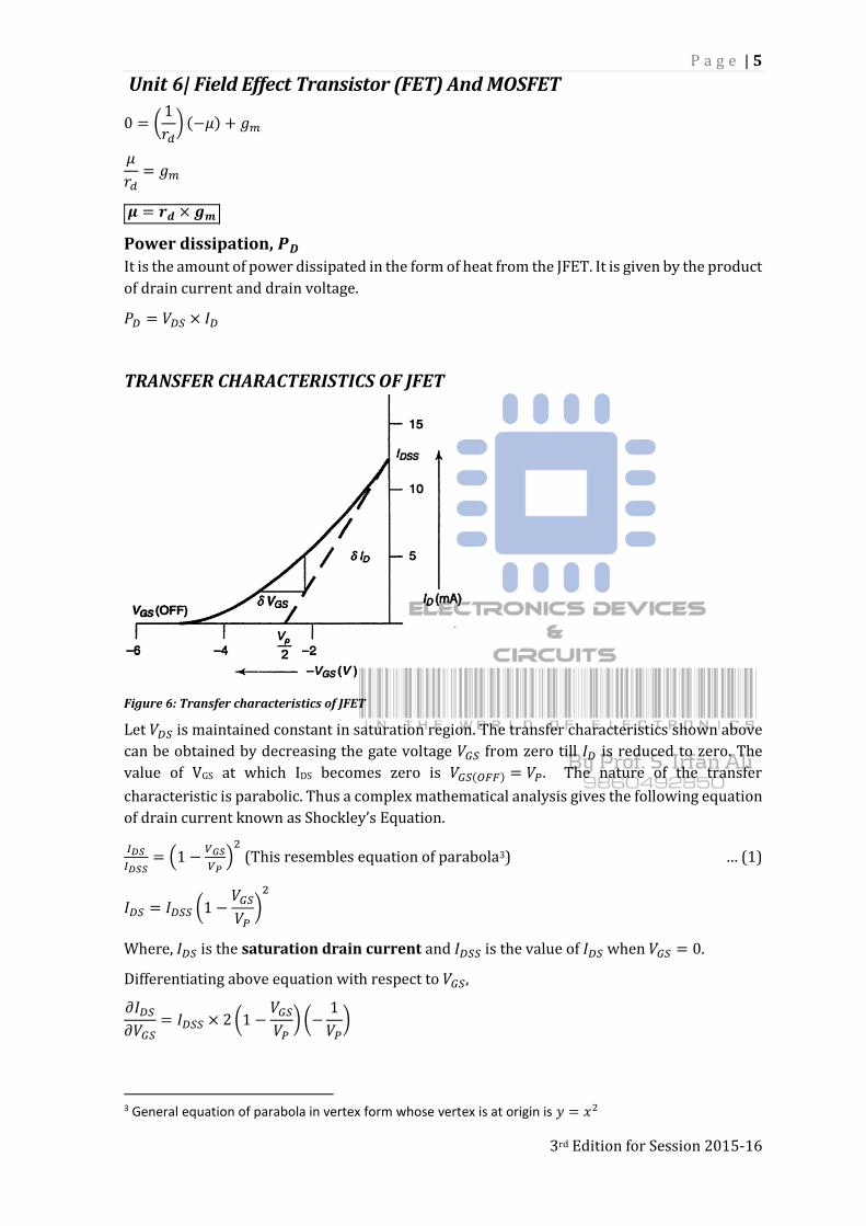
TRANSFER CHARACTERISTICS OF JFET
Figure 6: Transfer characteristics of JFET
Let 𝑉𝐷𝑆 is maintained constant in saturation region. The transfer characteristics shown above
can be obtained by decreasing the gate voltage 𝑉𝐺𝑆 from zero till 𝐼𝐷 is reduced to zero. The
value of VGS at which IDS becomes zero is 𝑉𝐺𝑆(𝑂𝐹𝐹) = 𝑉𝑃. The nature of the transfer
characteristic is parabolic. Thus a complex mathematical analysis gives the following equation
of drain current known as Shockley’s Equation.
𝐼𝐷𝑆
𝐼𝐷𝑆𝑆= (1 −
𝑉𝐺𝑆
𝑉𝑃)
2 (This resembles equation of parabola3) … (1)
𝐼𝐷𝑆 = 𝐼𝐷𝑆𝑆 (1 −𝑉𝐺𝑆
𝑉𝑃)
2
Where, 𝐼𝐷𝑆 is the saturation drain current and 𝐼𝐷𝑆𝑆 is the value of 𝐼𝐷𝑆 when 𝑉𝐺𝑆 = 0.
Differentiating above equation with respect to 𝑉𝐺𝑆,
𝜕𝐼𝐷𝑆
𝜕𝑉𝐺𝑆= 𝐼𝐷𝑆𝑆 × 2 (1 −
𝑉𝐺𝑆
𝑉𝑃) (−
1
𝑉𝑃)
3 General equation of parabola in vertex form whose vertex is at origin is 𝑦 = 𝑥2

P a g e | 6
Unit 6| Field Effect Transistor (FET) And MOSFET
3rd Edition for Session 2015-16
∵ 𝑔𝑚 = (𝜕𝐼𝐷𝑆
𝜕𝑉𝐺𝑆)
𝑉𝐷𝑆
𝑔𝑚 = −2𝐼𝐷𝑆𝑆
𝑉𝑃 (1 −
𝑉𝐺𝑆
𝑉𝑃) … (2)
Now rewriting equation (1),
𝐼𝐷𝑆
𝐼𝐷𝑆𝑆= (1 −
𝑉𝐺𝑆
𝑉𝑃)
2
∴ (1 −𝑉𝐺𝑆
𝑉𝑃) = √
𝐼𝐷𝑆
𝐼𝐷𝑆𝑆
Putting this value in equation (2)
∴ 𝑔𝑚 = −2𝐼𝐷𝑆𝑆
𝑉𝑃 √
𝐼𝐷𝑆
𝐼𝐷𝑆𝑆= −
2√𝐼𝐷𝑆×𝐼𝐷𝑆𝑆
𝑉𝑃 … (3)
Let 𝑔𝑚 = 𝑔𝑚0 when 𝑉𝐺𝑆 = 0 then from equation (2)
𝑔𝑚0 = −2𝐼𝐷𝑆𝑆
𝑉𝑃(1 −
0
𝑉𝑃)
𝑔𝑚0 = −2𝐼𝐷𝑆𝑆
𝑉𝑃
Equation (3) becomes,
𝑔𝑚 = 𝑔𝑚0√𝐼𝐷𝑆
𝐼𝐷𝑆𝑆
Or
𝑔𝑚 = 𝑔𝑚0 (1 −𝑉𝐺𝑆
𝑉𝑃)
Equation (3) can also be written as
𝑔𝑚 = −2√𝐼𝐷𝑆 × 𝐼𝐷𝑆𝑆
𝑉𝑃=
2
(−𝑉𝑃)√𝐼𝐷𝑆 × 𝐼𝐷𝑆𝑆
𝒈𝒎 =𝟐
|𝑽𝑷|√𝑰𝑫𝑺 × 𝑰𝑫𝑺𝑺
P a g e | 7
Unit 6| Field Effect Transistor (FET) And MOSFET
3rd Edition for Session 2015-16
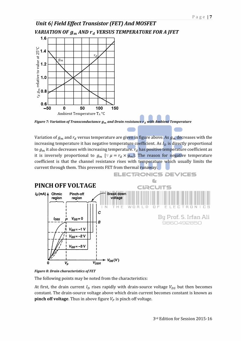
VARIATION OF 𝒈𝒎 AND 𝒓𝒅 VERSUS TEMPERATURE FOR A JFET
Figure 7: Variation of Transconductance 𝒈𝒎 and Drain resistance 𝒓𝒅 with Ambient Temperature
Variation of 𝑔𝑚 and 𝑟𝑑 versus temperature are given in figure above. As 𝑔𝑚 decreases with the
increasing temperature it has negative temperature coefficient. As 𝐼𝐷 is directly proportional
to 𝑔𝑚 it also decreases with increasing temperature. 𝑟𝑑 has positive temperature coefficient as
it is inversely proportional to 𝑔𝑚 [∵ 𝜇 = 𝑟𝑑 × 𝑔𝑚]. The reason for negative temperature
coefficient is that the channel resistance rises with temperature which usually limits the
current through them. This prevents FET from thermal runaway.
PINCH OFF VOLTAGE
Figure 8: Drain characteristics of FET
The following points may be noted from the characteristics:
At first, the drain current 𝐼𝐷 rises rapidly with drain-source voltage 𝑉𝐷𝑆 but then becomes
constant. The drain-source voltage above which drain current becomes constant is known as
pinch off voltage. Thus in above figure 𝑉𝑃 is pinch off voltage.

P a g e | 8
Unit 6| Field Effect Transistor (FET) And MOSFET
3rd Edition for Session 2015-16
After pinch off voltage 𝑉𝑃, the channel width becomes so narrow that depletion layers almost
touch each other. The drain current passes through the small passage between these layers.
Therefore, increase in drain current is very small with 𝑉𝐷𝑆 above pinch off voltage.
Consequently, drain current remains constant.
Figure 9: Basic structure of N-channel FET
Let ‘2𝑎’ be the channel height as shown in figure above then Pinch off voltage for p-channel
JFET is given by
|𝑉𝑃|𝑝 =𝑞 𝑁𝐴 𝑎2
2 𝜖
Pinch off voltage for n-channel JFET is given by
|𝑉𝑃|𝑛 =𝑞 𝑁𝐷 𝑎2
2 𝜖
Find the pinch off voltage of a silicon p-channel FET having half channel height of 2 microns and channel resistivity of 10 Ω-cm. Dielectric constant of silicon is 12 and mobility of holes is 500cm2/Vs. (5 marks) Solution:
Given:
𝐶ℎ𝑎𝑛𝑛𝑒𝑙 ℎ𝑒𝑖𝑔ℎ𝑡 = 2𝑎
ℎ𝑎𝑙𝑓 𝑐ℎ𝑎𝑛𝑛𝑒𝑙 ℎ𝑒𝑖𝑔ℎ𝑡 = 𝑎 = 2 𝑚𝑖𝑐𝑟𝑜𝑛𝑠 = 2 𝜇𝑚 = 𝟐 × 𝟏𝟎−𝟒 𝒄𝒎
𝜌 = 10 Ω𝑐𝑚
𝜇𝑝 = 500 𝑐𝑚2/𝑉𝑠
𝜖𝑟(𝑆𝑖)= 12
𝜖0 = 8.854 × 10⁻¹² 𝐹/𝑚 = 8.854 × 10⁻¹⁴ 𝐹/𝑐𝑚
𝜖 = 𝜖0𝜖𝑟 = 𝟖. 𝟖𝟓𝟒 × 𝟏𝟎−𝟏𝟒 × 𝟏𝟐
The pinch off voltage for p channel FET is given by
|𝑉𝑃|𝑝 =𝑞 𝑁𝐴 𝑎2
2 𝜖
𝜌 =1
𝜎=
1
𝑞(𝑝𝑝𝜇𝑝 + 𝑛𝑝𝜇𝑛)=
1
𝑝𝑝𝑞𝜇𝑝 (∵ 𝑝𝑝 ≫ 𝑛𝑝)

P a g e | 9
Unit 6| Field Effect Transistor (FET) And MOSFET
3rd Edition for Session 2015-16
Also 𝑝𝑝 = 𝑁𝐴
𝜌 =1
𝑁𝐴𝑞𝜇𝑝
𝑞𝑁𝐴 =1
𝜌𝜇𝑝=
1
10 × 500=
𝟏
𝟓𝟎𝟎𝟎
∴ |𝑉𝑃|𝑝 =𝑞 𝑁𝐴 𝑎2
2 𝜖=
1
5000× (2 × 10−4)2 ×
1
2 × (8.854 × 10−14 × 12)
𝑽𝑷 = 𝟑. 𝟕𝟔 𝑽
JFET AMPLIFIERS (CS, CD, CG)
JFET COMMON SOURCE (CS) AMPLIFIER
Figure 10: Common source amplifier circuit using FET
CS (Common Source) Amplifier ac model
Figure 11: Small-signal low-frequency model of FET
From the figure 11, the output voltage will be
𝑉𝑂 = 𝑖𝑑𝑟𝑑
Also
𝑉𝑂 = 𝑖𝑑 (𝑟𝑑𝑅𝑑
𝑟𝑑 + 𝑅𝑑) = 𝑖𝑑𝑟𝑑 (
𝑅𝑑
𝑟𝑑 + 𝑅𝑑)
We know, the amplification factor is given by
𝜇 = − (𝜕𝑉𝐷𝑆
𝜕𝑉𝐺𝑆)
𝐼𝐷
= −𝑜𝑢𝑡𝑜𝑢𝑡 𝑣𝑜𝑙𝑡𝑎𝑔𝑒
𝑖𝑛𝑝𝑢𝑡 𝑣𝑜𝑙𝑡𝑎𝑔𝑒= −
𝑉𝑂
𝑉𝑖= −
𝑖𝑑𝑟𝑑
𝑉𝑖
𝑖𝑑𝑟𝑑 = −𝜇𝑉𝑖
∴ 𝑉𝑂 = −𝜇𝑉𝑖𝑅𝑑
𝑟𝑑 + 𝑅𝑑
The voltage gain is given by,
P a g e | 10
Unit 6| Field Effect Transistor (FET) And MOSFET
3rd Edition for Session 2015-16
𝐴𝑉 =𝑉𝑂
𝑉𝑖
∴ 𝑨𝑽 = −𝝁𝑹𝒅
𝒓𝒅 + 𝑹𝒅
∵ 𝜇 = 𝑟𝑑 × 𝑔𝑚
𝐴𝑉 = −𝑟𝑑𝑔𝑚𝑅𝑑
𝑟𝑑 + 𝑅𝑑= −𝑔𝑚 (
𝑟𝑑𝑅𝑑
𝑟𝑑 + 𝑅𝑑) = −𝑔𝑚𝑅𝑑
′
Where, 𝑅𝑑′ = 𝑅𝑑||𝑟𝑑
𝑨𝑽 = −𝒈𝒎𝑹𝒅′
Negative sign indicates that output is 180° out of phase with the input.
This is the expression for voltage gain at low frequency.
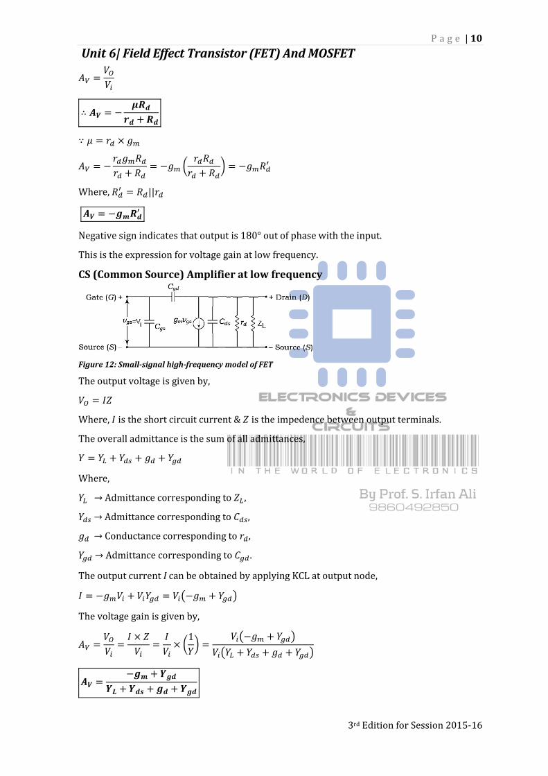
CS (Common Source) Amplifier at low frequency
Figure 12: Small-signal high-frequency model of FET
The output voltage is given by,
𝑉𝑂 = 𝐼𝑍
Where, 𝐼 is the short circuit current & 𝑍 is the impedence between output terminals.
The overall admittance is the sum of all admittances,
𝑌 = 𝑌𝐿 + 𝑌𝑑𝑠 + 𝑔𝑑 + 𝑌𝑔𝑑
Where,
𝑌𝐿 → Admittance corresponding to 𝑍𝐿 ,
𝑌𝑑𝑠 → Admittance corresponding to 𝐶𝑑𝑠,
𝑔𝑑 → Conductance corresponding to 𝑟𝑑,
𝑌𝑔𝑑 → Admittance corresponding to 𝐶𝑔𝑑.
The output current I can be obtained by applying KCL at output node,
𝐼 = −𝑔𝑚𝑉𝑖 + 𝑉𝑖𝑌𝑔𝑑 = 𝑉𝑖(−𝑔𝑚 + 𝑌𝑔𝑑)
The voltage gain is given by,
𝐴𝑉 =𝑉𝑂
𝑉𝑖=
𝐼 × 𝑍
𝑉𝑖=
𝐼
𝑉𝑖× (
1
𝑌) =
𝑉𝑖(−𝑔𝑚 + 𝑌𝑔𝑑)
𝑉𝑖(𝑌𝐿 + 𝑌𝑑𝑠 + 𝑔𝑑 + 𝑌𝑔𝑑)
𝑨𝑽 =−𝒈𝒎 + 𝒀𝒈𝒅
𝒀𝑳 + 𝒀𝒅𝒔 + 𝒈𝒅 + 𝒀𝒈𝒅
P a g e | 11
Unit 6| Field Effect Transistor (FET) And MOSFET
3rd Edition for Session 2015-16
This is the expression for voltage gain at high frequency.
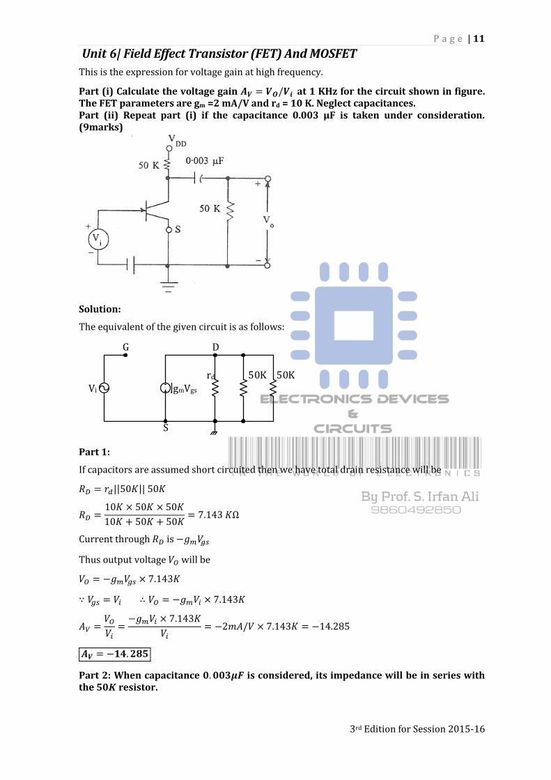
Part (i) Calculate the voltage gain 𝑨𝑽 = 𝑽𝑶/𝑽𝒊 at 1 KHz for the circuit shown in figure. The FET parameters are gm =2 mA/V and rd = 10 K. Neglect capacitances. Part (ii) Repeat part (i) if the capacitance 0.003 μF is taken under consideration. (9marks)
Solution:
The equivalent of the given circuit is as follows:
gmVgsVi
rd 50K 50K
D
S
G
Part 1:
If capacitors are assumed short circuited then we have total drain resistance will be
𝑅𝐷 = 𝑟𝑑||50𝐾|| 50𝐾
𝑅𝐷 =10𝐾 × 50𝐾 × 50𝐾
10𝐾 + 50𝐾 + 50𝐾= 7.143 𝐾Ω
Current through 𝑅𝐷 is −𝑔𝑚𝑉𝑔𝑠
Thus output voltage 𝑉𝑂 will be
𝑉𝑂 = −𝑔𝑚𝑉𝑔𝑠 × 7.143𝐾
∵ 𝑉𝑔𝑠 = 𝑉𝑖 ∴ 𝑉𝑂 = −𝑔𝑚𝑉𝑖 × 7.143𝐾
𝐴𝑉 =𝑉𝑂
𝑉𝑖=
−𝑔𝑚𝑉𝑖 × 7.143𝐾
𝑉𝑖= −2𝑚𝐴/𝑉 × 7.143𝐾 = −14.285
𝑨𝑽 = −𝟏𝟒. 𝟐𝟖𝟓
Part 2: When capacitance 𝟎. 𝟎𝟎𝟑𝝁𝑭 is considered, its impedance will be in series with the 𝟓𝟎𝑲 resistor.

P a g e | 12
Unit 6| Field Effect Transistor (FET) And MOSFET
3rd Edition for Session 2015-16
𝑋𝐶 =1
𝑗𝜔𝐶=
1
𝑗2𝜋𝑓𝐶=
1
𝑗2𝜋(1𝐾𝐻𝑧)(0.003𝜇𝐹)=
53𝐾
𝑗= −𝑗 53𝐾
gmVgsVi
rd||50K8.33K
RL=50K
D
S
G
XC=53K/j
IL
VO
ZL
V
Voltage across Drain and Source is given by,
𝑉 = (−𝑔𝑚𝑉𝑔𝑠) (8.33𝐾 × 𝑍𝐿
8.33𝐾 + 𝑍𝐿)
𝐼𝐿 =𝑉
𝑍𝐿=
(−𝑔𝑚𝑉𝑔𝑠) (8.33𝐾 × 𝑍𝐿8.33𝐾 + 𝑍𝐿
)
𝑍𝐿= −𝑔𝑚𝑉𝑔𝑠 ×
8.33𝐾
8.33𝐾 + 𝑍𝐿
𝑉𝑂 = 𝐼𝐿𝑅𝐿 = −𝑔𝑚𝑉𝑔𝑠 ×8.33𝐾
8.33𝐾 + 𝑍𝐿× 𝑅𝐿 = −𝑔𝑚𝑉𝑖 ×
8.33𝐾
8.33𝐾 + 𝑍𝐿× 𝑅𝐿
𝐴𝑉 =𝑉𝑂
𝑉𝑖= −𝑔𝑚𝑅𝐿 ×
8.33𝐾
8.33𝐾 + 𝑍𝐿= −(2𝑚𝐴/𝑉)(50𝐾Ω) ×
8.33𝐾
8.33𝐾 + 𝑍𝐿
𝐴𝑉 = −(2𝑚𝐴/𝑉)(50𝐾Ω) ×8.33𝐾
8.33𝐾 + (𝑅𝐿 + 𝑋𝐶)
𝐴𝑉 = −(2𝑚𝐴/𝑉)(50𝐾Ω) ×8.33𝐾
8.33𝐾 + 50𝐾 + (−𝑗 53𝐾)= −(2𝑚𝐴/𝑉)(50𝐾Ω) ×
8.33𝐾
58.33𝐾 − 𝑗 53𝐾
𝐴𝑉 = −7.82 − 𝑗 7.1
𝑨𝑽 = 𝟏𝟎. 𝟓𝟔𝟗∠ − 𝟏𝟑𝟕°𝟕𝟒′
BIASING THE FET For proper functioning of a linear FET amplifier, it is necessary to maintain the operating point
(Q-Point) stable in the central portion of the pinch off region. The Q-point should be
independent of device parameter variations and ambient temperature changes. This can be
achieved by suitably selecting the gate to source voltage 𝑉𝑔𝑠 and drain current 𝐼𝐷, which is
referred to as biasing.
The FET may be used in following three biasing techniques:
1. Self-Bias
2. Voltage Divider Bias
3. Fixed Bias
P a g e | 13
Unit 6| Field Effect Transistor (FET) And MOSFET
3rd Edition for Session 2015-16
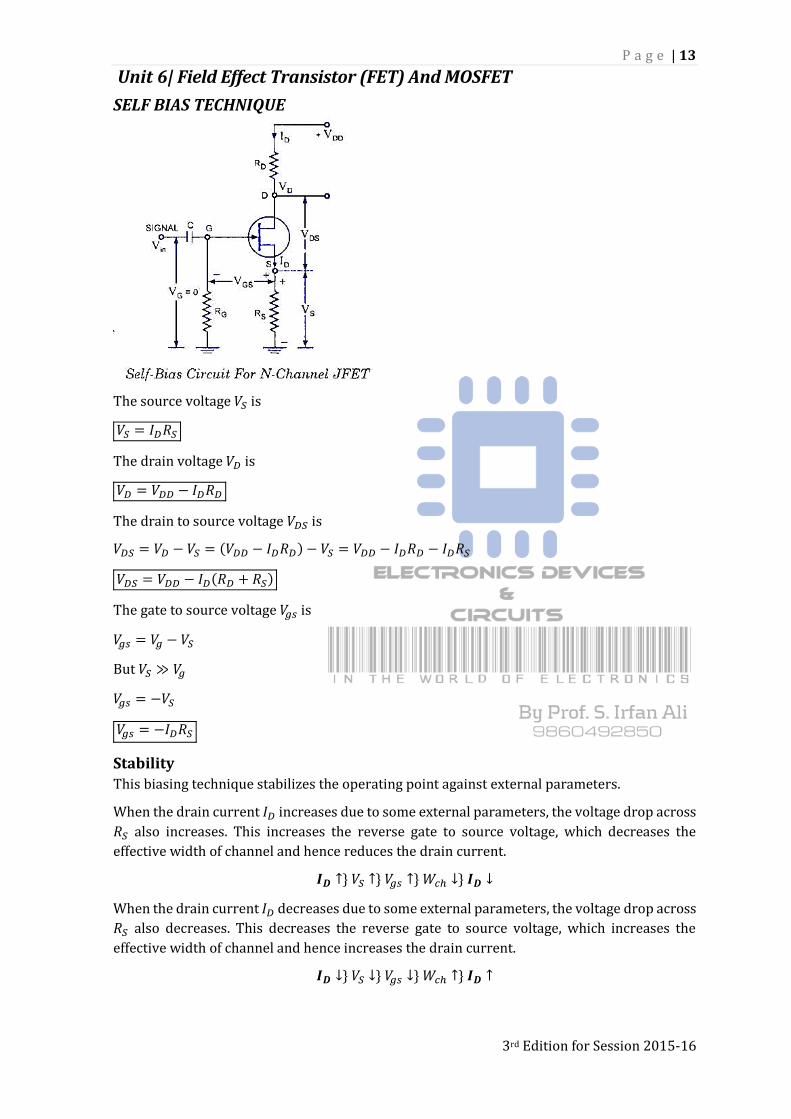
SELF BIAS TECHNIQUE
The source voltage 𝑉𝑆 is
𝑉𝑆 = 𝐼𝐷𝑅𝑆
The drain voltage 𝑉𝐷 is
𝑉𝐷 = 𝑉𝐷𝐷 − 𝐼𝐷𝑅𝐷
The drain to source voltage 𝑉𝐷𝑆 is
𝑉𝐷𝑆 = 𝑉𝐷 − 𝑉𝑆 = (𝑉𝐷𝐷 − 𝐼𝐷𝑅𝐷) − 𝑉𝑆 = 𝑉𝐷𝐷 − 𝐼𝐷𝑅𝐷 − 𝐼𝐷𝑅𝑆
𝑉𝐷𝑆 = 𝑉𝐷𝐷 − 𝐼𝐷(𝑅𝐷 + 𝑅𝑆)
The gate to source voltage 𝑉𝑔𝑠 is
𝑉𝑔𝑠 = 𝑉𝑔 − 𝑉𝑆
But 𝑉𝑆 ≫ 𝑉𝑔
𝑉𝑔𝑠 = −𝑉𝑆
𝑉𝑔𝑠 = −𝐼𝐷𝑅𝑆
Stability
This biasing technique stabilizes the operating point against external parameters.
When the drain current 𝐼𝐷 increases due to some external parameters, the voltage drop across
𝑅𝑆 also increases. This increases the reverse gate to source voltage, which decreases the
effective width of channel and hence reduces the drain current.
𝑰𝑫 ↑ 𝑉𝑆 ↑ 𝑉𝑔𝑠 ↑ 𝑊𝑐ℎ ↓ 𝑰𝑫 ↓
When the drain current 𝐼𝐷 decreases due to some external parameters, the voltage drop across
𝑅𝑆 also decreases. This decreases the reverse gate to source voltage, which increases the
effective width of channel and hence increases the drain current.
𝑰𝑫 ↓ 𝑉𝑆 ↓ 𝑉𝑔𝑠 ↓ 𝑊𝑐ℎ ↑ 𝑰𝑫 ↑

P a g e | 14
Unit 6| Field Effect Transistor (FET) And MOSFET
3rd Edition for Session 2015-16
VOLTAGE DIVIDER BIASING TECHNIQUE
The resistors 𝑅𝐺1 & 𝑅𝐺2 form a voltage divider network that can be simplified to its Thevenin’s
equivalent. Thus the Thevenin’s voltage 𝑉𝐺𝐺 and Thevenin’s resistor 𝑅𝐺 will be
𝑉𝐺𝐺 = (𝑅1
𝑅1 + 𝑅2) 𝑉𝐷𝐷
𝑅𝐺 =𝑅1𝑅2
𝑅1 + 𝑅2
FIXED BIASING TECHNIQUE
The fixed bias for n channel JFET is obtained by using a supply 𝑉𝐺𝐺. This supply ensures that
the gate is always negative with respect to source and no current flows through resistance 𝑅𝐺
and gate terminal 𝑖. 𝑒. 𝐼𝐺 = 0. The gate to source voltage is
𝑉𝐺𝑆 = 𝑉𝐺 − 𝑉𝑆 = (−𝑉𝐺𝐺) − 0 ∴ 𝑉𝐺𝑆 = −𝑉𝐺𝐺
The drain current is
𝐼𝐷 =𝑉𝐷𝐷 − 𝑉𝐷𝑆
𝑅𝐷

P a g e | 15
Unit 6| Field Effect Transistor (FET) And MOSFET
3rd Edition for Session 2015-16
The CS amplifier stage has following parameters : — 𝑹𝒅 = 𝟏𝟐𝑲, 𝑹𝒈 = 𝟏𝑴, 𝑹𝒔 = 𝟒𝟕𝟎Ω, 𝑽𝑫𝑫 = 𝟑𝟎𝑽. 𝑪𝒔 is very large.
𝑰𝑫𝑺𝑺 = 𝟑𝒎𝑨, 𝑽𝑷 = −𝟐. 𝟒𝑽, 𝒓𝒅 >> 𝑹𝑫. Determine: (i) Gate to source bias 𝑽𝒈𝒔
(ii) Drain current 𝑰𝑫
(iii) Voltage 𝑽𝑫𝑺. (iv) Small signal voltage gain 𝑨𝑽.
Solution:
RD
RSRg CS
CC
VO
Vi
VDD=30V
ID
ID
Ig
Part 1:
We know,
𝐼𝐷 = 𝐼𝐷𝑆𝑆 (1 −𝑉𝑔𝑠
𝑉𝑃)
2
Applying KVL in gate loop
𝐼𝑔𝑅𝑔 − 𝑉𝑔𝑠 − 𝐼𝐷𝑅𝑆 = 0
But ideally, 𝐼𝑔 = 0
𝑉𝑔𝑠 = −𝐼𝐷𝑅𝑆
𝐼𝐷 = −𝑉𝑔𝑠
𝑅𝑆
−𝑉𝑔𝑠
𝑅𝑆= 𝐼𝐷𝑆𝑆 (1 −
𝑉𝑔𝑠
𝑉𝑃)
2
P a g e | 16
Unit 6| Field Effect Transistor (FET) And MOSFET
3rd Edition for Session 2015-16
−𝑉𝑔𝑠
𝑅𝑆= 𝐼𝐷𝑆𝑆 (1 − 2 ×
𝑉𝑔𝑠
𝑉𝑃+
𝑉𝑔𝑠2
𝑉𝑃2)
𝑉𝑔𝑠2
𝑉𝑃2 × 𝐼𝐷𝑆𝑆 − 2 ×
𝑉𝑔𝑠
𝑉𝑃× 𝐼𝐷𝑆𝑆 + 𝐼𝐷𝑆𝑆 +
𝑉𝑔𝑠
𝑅𝑆= 0
(𝐼𝐷𝑆𝑆
𝑉𝑃2 ) × 𝑉𝑔𝑠
2 + (1
𝑅𝑆−
2𝐼𝐷𝑆𝑆
𝑉𝑃) × 𝑉𝑔𝑠 + 𝐼𝐷𝑆𝑆 = 0
(3𝑚𝐴
(−2.4)2) × 𝑉𝑔𝑠
2 + (1
470−
2 × 3𝑚𝐴
−2.4) × 𝑉𝑔𝑠 + (3𝑚𝐴) = 0
This is the equation of 2nd order. Its solution can be obtained by −𝑏±√𝑏2−4𝑎𝑐
2𝑎,
𝑉𝑔𝑠1= −0.704 𝑉
𝑉𝑔𝑠2= −8.18 𝑉
But 𝑉𝑔𝑠 = −𝐼𝐷𝑅𝑆 and the maximum value of 𝐼𝐷 can be only 𝐼𝐷𝑆𝑆, therefore maximum magnitude
of 𝑉𝑔𝑠 can be decided using 𝐼𝐷𝑆𝑆. 𝑉𝑔𝑠 = −𝐼𝐷𝑆𝑆𝑅𝑆 = −3𝑚 × 470 = −1.41. Therefore, the value of
𝑉𝑔𝑠 cannot go beyond −1.41.
Thus the gate to source voltage will be,
𝑉𝑔𝑠 = −0.704 𝑉 = −0.7 𝑉
Part 2:
The drain current is given by,
𝐼𝐷 = 𝐼𝐷𝑆𝑆 (1 −𝑉𝑔𝑠
𝑉𝑃)
2
𝐼𝐷 = 3𝑚 (1 −−0.7
−2.4)
2
𝐼𝐷 = 1.505 𝑚𝐴
Part 3:
Now to find 𝑉𝐷𝑆, we have to apply KVL from 𝑉𝐷𝐷 to Ground.
𝑉𝐷𝐷 − 𝐼𝐷𝑅𝐷 − 𝑉𝐷𝑆 − 𝐼𝐷𝑅𝑆 = 0
𝑉𝐷𝑆 = 𝑉𝐷𝐷 − 𝐼𝐷(𝑅𝐷 + 𝑅𝑆) = 30 − 1.505𝑚(12𝐾 + 470)
𝑉𝐷𝑆 = 11.30 𝑉
Part 4:
We know,
𝐴𝑉 = −𝑔𝑚𝑅𝑑
And
𝑔𝑚 = 𝑔𝑚0 (1 −𝑉𝑔𝑠
𝑉𝑃)
Also,
P a g e | 17
Unit 6| Field Effect Transistor (FET) And MOSFET
3rd Edition for Session 2015-16
𝑔𝑚0 = −2𝐼𝐷𝑆𝑆
𝑉𝑃= −
2 × 3𝑚
(−2.4)= 2.5 × 10⁻³
𝑔𝑚 = 2.5 × 10⁻³ (1 −−0.7
−2.4) = 1.77 × 10⁻³ 𝐴/𝑉
𝐴𝑉 = −1.77 × 10−3 × 12𝐾
𝐴𝑉 = −21.24
A bias circuit using FET is shown in the figure. Determine the quiescent value of 𝑽𝑫𝑺, 𝑽𝑮𝑺 and 𝑰𝑫. Given that 𝑽𝑷 = 𝟓 𝑽 and 𝑰𝑫𝑺𝑺 = 𝟓 𝒎𝑨. (7 marks)
RD=2K
RS=5K CS
VO
Vi
VDD=10V
Solution:
To find 𝑽𝑫𝑺:
Applying KVL from 𝑉𝐷𝐷 to Ground,
𝑉𝐷𝐷 − 𝐼𝐷𝑅𝐷 − 𝑉𝐷𝑆 − 𝐼𝐷𝑅𝑆 = 0
𝑉𝐷𝑆 = 𝑉𝐷𝐷 − 𝐼𝐷(𝑅𝐷 + 𝑅𝑆)
𝑉𝐷𝑆 = 10 − 𝐼𝐷(2𝐾 + 5𝐾) --- (1)
Now to find 𝐼𝐷, we know,
𝐼𝐷 = 𝐼𝐷𝑆𝑆 (1 −𝑉𝑔𝑠
𝑉𝑃)
2
& 𝑉𝑔𝑠 = −𝐼𝐷𝑅𝑆
𝐼𝐷 = 𝐼𝐷𝑆𝑆 (1 −−𝐼𝐷𝑅𝑆
𝑉𝑃)
2
𝐼𝐷 = 5𝑚 (1 −−𝐼𝐷 × 5𝐾
−5)
2
𝐼𝐷 = 5𝑚 (1 − 𝐼𝐷 × 1000)2
𝐼𝐷 = 5𝑚 (1 − 2 × 𝐼𝐷 × 1000 + 10002𝐼𝐷2)
𝐼𝐷 = 5𝑚 − 5𝑚 × 2 × 𝐼𝐷 × 1000 + 5𝑚 × 10002𝐼𝐷2
5000 𝐼𝐷2 − (5𝑚 × 2 × 1000 + 1)𝐼𝐷 + 5𝑚 = 0
5000 𝐼𝐷2 − 11 𝐼𝐷 + 5𝑚 = 0
The solution of above quadratic equation can be obtained using −𝑏±√𝑏2−4𝑎𝑐
2𝑎,
P a g e | 18
Unit 6| Field Effect Transistor (FET) And MOSFET
3rd Edition for Session 2015-16
𝐼𝐷1= 1.558 𝑚𝐴 & 𝐼𝐷2
= 641.74 𝜇𝐴
Now from equation (1),
𝑉𝐷𝑆 = 10 − 𝐼𝐷1(2𝐾 + 5𝐾) = 10 − (1.558𝑚)(2𝐾 + 5𝐾) = −0.906 𝑉
But 𝑉𝐷𝑆 cannot be negative; therefore 𝐼𝐷1 is invalid,
∴ 𝑉𝐷𝑆 = 10 − 𝐼𝐷2(2𝐾 + 5𝐾) = 10 − (641.74 𝜇)(2𝐾 + 5𝐾)
𝑉𝐷𝑆 = 5.5078 𝑉
To find 𝑽𝒈𝒔
We know,
𝑉𝑔𝑠 = −𝐼𝐷2𝑅𝑆 = −(641.74 𝜇)5𝐾
𝑉𝑔𝑠 = −3.209 𝑉
𝐼𝐷 = 641.74 𝜇𝐴
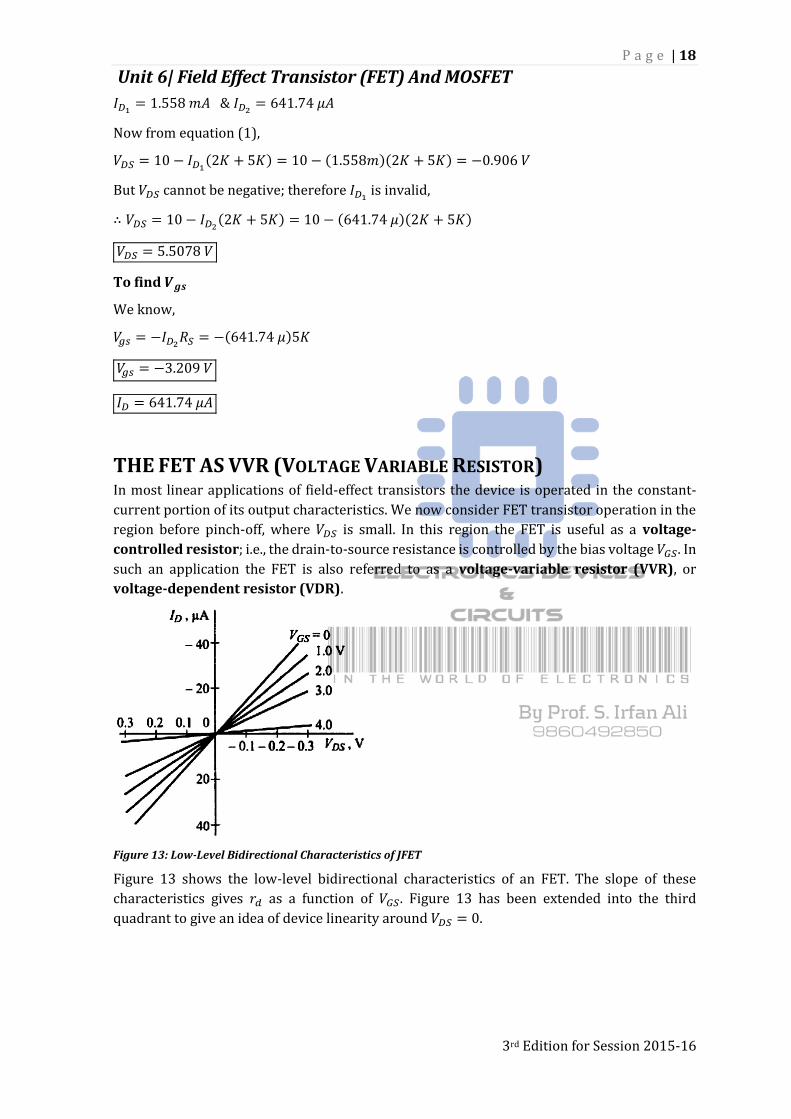
THE FET AS VVR (VOLTAGE VARIABLE RESISTOR) In most linear applications of field-effect transistors the device is operated in the constant-
current portion of its output characteristics. We now consider FET transistor operation in the
region before pinch-off, where 𝑉𝐷𝑆 is small. In this region the FET is useful as a voltage-
controlled resistor; i.e., the drain-to-source resistance is controlled by the bias voltage 𝑉𝐺𝑆. In
such an application the FET is also referred to as a voltage-variable resistor (VVR), or
voltage-dependent resistor (VDR).
Figure 13: Low-Level Bidirectional Characteristics of JFET
Figure 13 shows the low-level bidirectional characteristics of an FET. The slope of these
characteristics gives 𝑟𝑑 as a function of 𝑉𝐺𝑆. Figure 13 has been extended into the third
quadrant to give an idea of device linearity around 𝑉𝐷𝑆 = 0.

P a g e | 19
Unit 6| Field Effect Transistor (FET) And MOSFET
3rd Edition for Session 2015-16
Figure 14: Variation of 𝒓𝒅 with 𝑽𝒈𝒔
The variation of 𝑟𝑑 with 𝑉𝑔𝑠 is plotted in figure 14 for the 2N3277 and 2N3278 FETs. The
variation of 𝑟𝑑 with 𝑉𝑔𝑠 can be closely approximated by the following equation,
𝑟𝑑 =𝑟𝑜
1 − 𝐾𝑉𝑔𝑠
Where,
𝑟𝑜 → Drain resistance at zero gate bias
𝐾 → A constant, dependent upon FET type
𝑉𝑔𝑠 → Gate to source voltage
JFET AS AGC (AUTOMATIC GAIN CONTROL) The voltage variable resistor property of
FET can be used to vary the voltage gain of
a multistage amplifier A as the signal level
is increased. This action is called
automatic gain control (AGC). This is
illustrated in Fig. 15. Here, maximum value
of signal is taken, rectified, and filtered to
produce a dc voltage proportional to the
output signal level. This voltage is applied
to the gate of JFET, thus causing the ac
resistance between the drain and source
to change. As this resistance is connected
across 𝑅𝑒 , effective 𝑅𝑒 also changes according to change in the drain to source resistance. When
output signal level increases, the drain to source resistance also increases, increasing effective
𝑅𝑒 . Increase in 𝑅𝑒 causes the gain of transistor 𝑄1 to decrease reducing the output signal.
Exactly reverse process takes place when output signal level decreases. Therefore, the output
signal level is maintained constant. It is important to note that the dc bias conditions of 𝑄1 are
not affected by JFET since FET is isolated from 𝑄1 by means of capacitor 𝐶2.
Figure 15: Application of FET as VVR in AGC
P a g e | 20
Unit 6| Field Effect Transistor (FET) And MOSFET
3rd Edition for Session 2015-16
METAL OXIDE SEMICONDUCTOR4 FET (MOSFET) The main drawback of JFET is that its gate must be reverse biased for proper operation of the
device i.e. it can only have negative gate operation for n-channel and positive gate operation
for p-channel. This means that we can only decrease the width of the channel (i.e. decrease the
conductivity of the channel) from its zero-bias size. This type of operation is referred to as
depletion-mode operation. Therefore, a JFET can only be operated in the depletion-mode.
However, there is a field effect transistor (FET) that can be operated to enhance (or increase)
the width of the channel (with consequent increase in conductivity of the channel) i.e. it can
have enhancement-mode operation. Such a FET is called MOSFET.
Based on the construction MOSFETs are classified into following two types,
1. Depletion-Type MOSFET or D-MOSFET: It can be operated in both the depletion-mode
and the Enhancement-mode. For this reason, a D-MOSFET is sometimes called as
Depletion/Enhancement MOSFET.
2. Enhancement-Type MOSFET or E-MOSFET: It can be operated only in Enhancement-
mode.
Based on the type of channel (p or n) MOSFETs are classified into following two types,
1. n-Channel MOSFET or n-MOSFET: In this type of MOSFET, the channel is of n type.
2. p-Channel MOSFET or p-MOSFET: In this type of MOSFET, the channel is of p type.
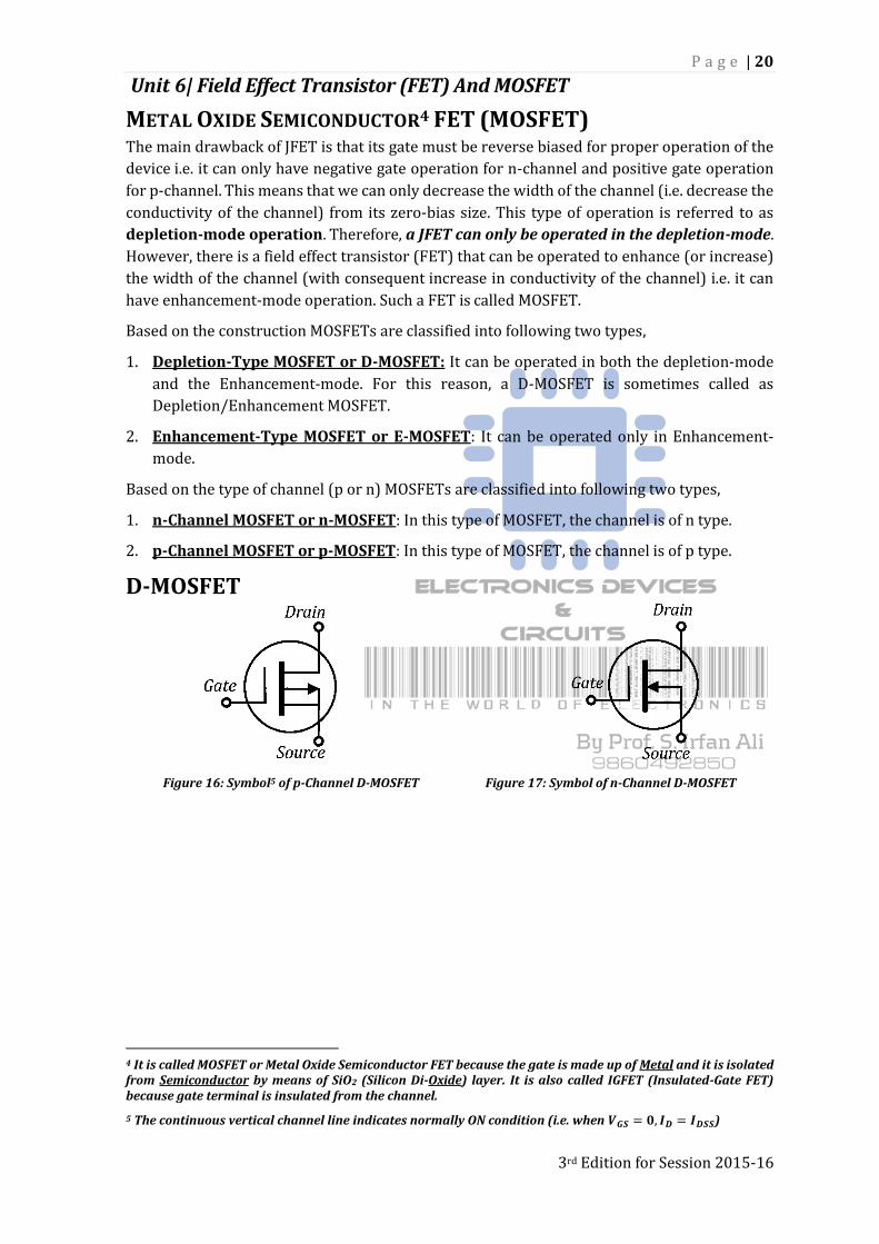
D-MOSFET
Figure 16: Symbol5 of p-Channel D-MOSFET Figure 17: Symbol of n-Channel D-MOSFET
4 It is called MOSFET or Metal Oxide Semiconductor FET because the gate is made up of Metal and it is isolated from Semiconductor by means of SiO2 (Silicon Di-Oxide) layer. It is also called IGFET (Insulated-Gate FET) because gate terminal is insulated from the channel.
5 The continuous vertical channel line indicates normally ON condition (i.e. when 𝑽𝑮𝑺 = 𝟎, 𝑰𝑫 = 𝑰𝑫𝑺𝑺)
P a g e | 21
Unit 6| Field Effect Transistor (FET) And MOSFET
3rd Edition for Session 2015-16
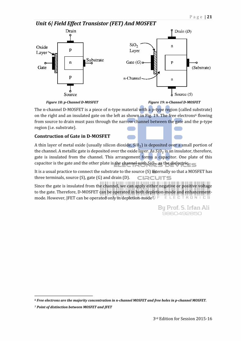
Figure 18: p-Channel D-MOSFET Figure 19: n-Channel D-MOSFET
The n-channel D-MOSFET is a piece of n-type material with a p-type region (called substrate)
on the right and an insulated gate on the left as shown in Fig. 19. The free electrons6 flowing
from source to drain must pass through the narrow channel between the gate and the p-type
region (i.e. substrate).
Construction of Gate in D-MOSFET
A thin layer of metal oxide (usually silicon dioxide, 𝑆𝑖02) is deposited over a small portion of
the channel. A metallic gate is deposited over the oxide layer. As 𝑆𝑖02 is an insulator, therefore,
gate is insulated from the channel. This arrangement forms a capacitor. One plate of this
capacitor is the gate and the other plate is the channel with 𝑆𝑖𝑂2, as the dielectric.
It is a usual practice to connect the substrate to the source (S) internally so that a MOSFET has
three terminals, source (S), gate (G) and drain (D).
Since the gate is insulated from the channel, we can apply either negative or positive voltage
to the gate. Therefore, D-MOSFET can be operated in both depletion-mode and enhancement-
mode. However, JFET can be operated only in depletion-mode7.
6 Free electrons are the majority concentration in n-channel MOSFET and free holes in p-channel MOSFET.
7 Point of distinction between MOSFET and JFET
P a g e | 22
Unit 6| Field Effect Transistor (FET) And MOSFET
3rd Edition for Session 2015-16
Transfer Characteristics of D-MOSFET
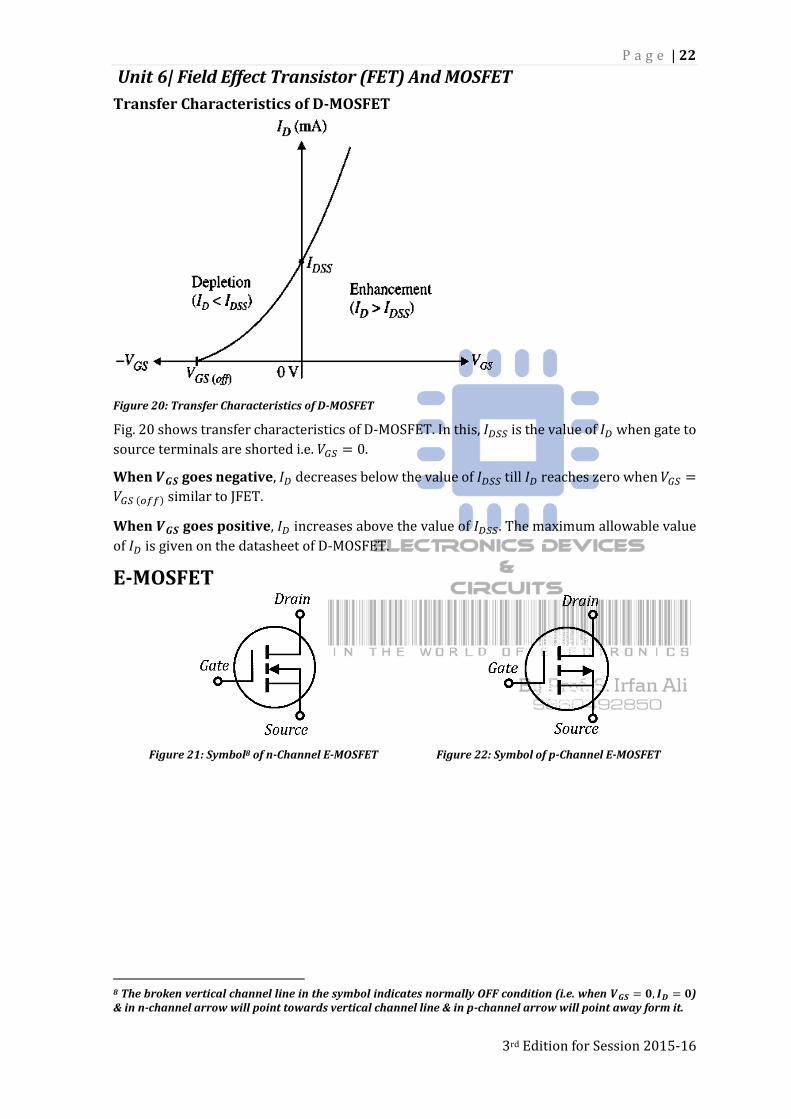
Figure 20: Transfer Characteristics of D-MOSFET
Fig. 20 shows transfer characteristics of D-MOSFET. In this, 𝐼𝐷𝑆𝑆 is the value of 𝐼𝐷 when gate to
source terminals are shorted i.e. 𝑉𝐺𝑆 = 0.
When 𝑽𝑮𝑺 goes negative, 𝐼𝐷 decreases below the value of 𝐼𝐷𝑆𝑆 till 𝐼𝐷 reaches zero when 𝑉𝐺𝑆 =
𝑉𝐺𝑆 (𝑜𝑓𝑓) similar to JFET.
When 𝑽𝑮𝑺 goes positive, 𝐼𝐷 increases above the value of 𝐼𝐷𝑆𝑆. The maximum allowable value
of 𝐼𝐷 is given on the datasheet of D-MOSFET.
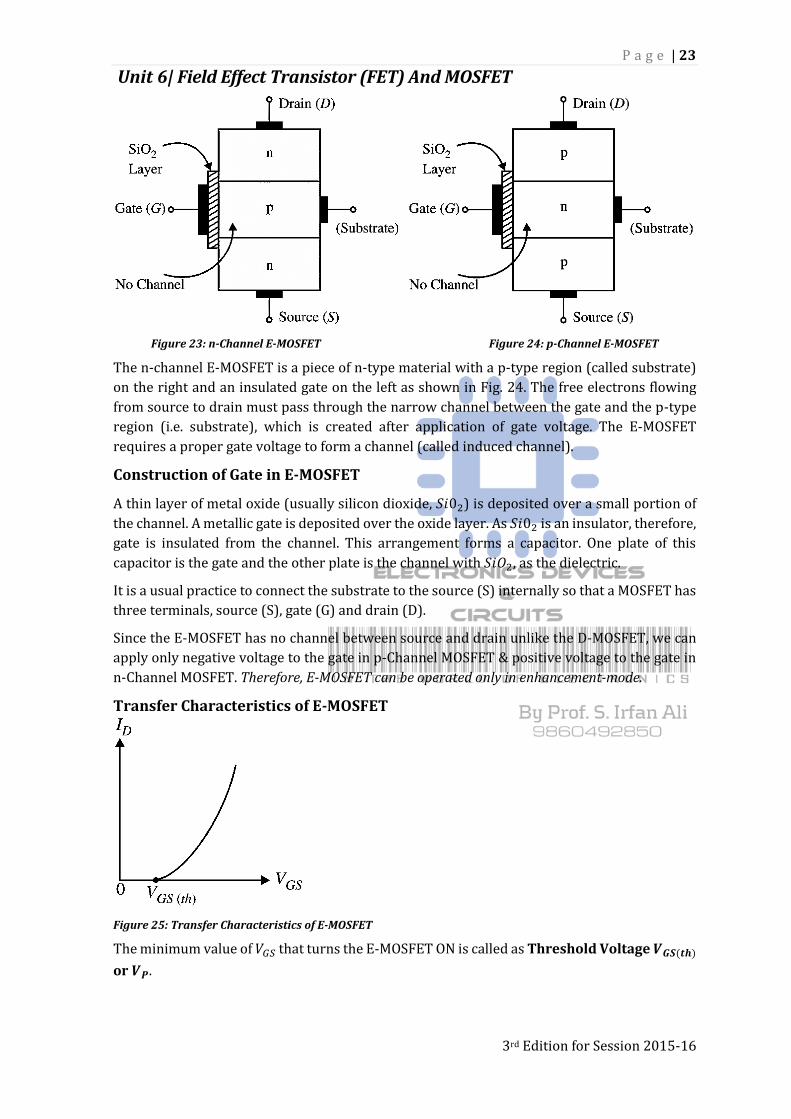
E-MOSFET
Figure 21: Symbol8 of n-Channel E-MOSFET Figure 22: Symbol of p-Channel E-MOSFET
8 The broken vertical channel line in the symbol indicates normally OFF condition (i.e. when 𝑽𝑮𝑺 = 𝟎, 𝑰𝑫 = 𝟎) & in n-channel arrow will point towards vertical channel line & in p-channel arrow will point away form it.
P a g e | 23
Unit 6| Field Effect Transistor (FET) And MOSFET
3rd Edition for Session 2015-16
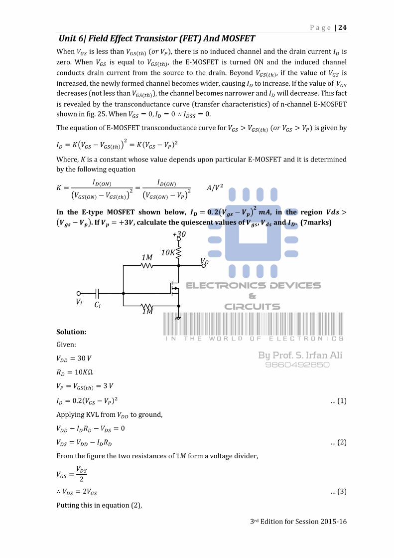
Figure 23: n-Channel E-MOSFET Figure 24: p-Channel E-MOSFET
The n-channel E-MOSFET is a piece of n-type material with a p-type region (called substrate)
on the right and an insulated gate on the left as shown in Fig. 24. The free electrons flowing
from source to drain must pass through the narrow channel between the gate and the p-type
region (i.e. substrate), which is created after application of gate voltage. The E-MOSFET
requires a proper gate voltage to form a channel (called induced channel).
Construction of Gate in E-MOSFET
A thin layer of metal oxide (usually silicon dioxide, 𝑆𝑖02) is deposited over a small portion of
the channel. A metallic gate is deposited over the oxide layer. As 𝑆𝑖02 is an insulator, therefore,
gate is insulated from the channel. This arrangement forms a capacitor. One plate of this
capacitor is the gate and the other plate is the channel with 𝑆𝑖𝑂2, as the dielectric.
It is a usual practice to connect the substrate to the source (S) internally so that a MOSFET has
three terminals, source (S), gate (G) and drain (D).
Since the E-MOSFET has no channel between source and drain unlike the D-MOSFET, we can
apply only negative voltage to the gate in p-Channel MOSFET & positive voltage to the gate in
n-Channel MOSFET. Therefore, E-MOSFET can be operated only in enhancement-mode.
Transfer Characteristics of E-MOSFET
Figure 25: Transfer Characteristics of E-MOSFET
The minimum value of 𝑉𝐺𝑆 that turns the E-MOSFET ON is called as Threshold Voltage 𝑽𝑮𝑺(𝒕𝒉)
or 𝑽𝑷.
P a g e | 24
Unit 6| Field Effect Transistor (FET) And MOSFET
3rd Edition for Session 2015-16
When 𝑉𝐺𝑆 is less than 𝑉𝐺𝑆(𝑡ℎ) (𝑜𝑟 𝑉𝑃), there is no induced channel and the drain current 𝐼𝐷 is
zero. When 𝑉𝐺𝑆 is equal to 𝑉𝐺𝑆(𝑡ℎ), the E-MOSFET is turned ON and the induced channel
conducts drain current from the source to the drain. Beyond 𝑉𝐺𝑆(𝑡ℎ), if the value of 𝑉𝐺𝑆 is
increased, the newly formed channel becomes wider, causing 𝐼𝐷 to increase. If the value of 𝑉𝐺𝑆
decreases (not less than 𝑉𝐺𝑆(𝑡ℎ)), the channel becomes narrower and 𝐼𝐷 will decrease. This fact
is revealed by the transconductance curve (transfer characteristics) of n-channel E-MOSFET
shown in fig. 25. When 𝑉𝐺𝑆 = 0, 𝐼𝐷 = 0 ∴ 𝐼𝐷𝑆𝑆 = 0.
The equation of E-MOSFET transconductance curve for 𝑉𝐺𝑆 > 𝑉𝐺𝑆(𝑡ℎ) (𝑜𝑟 𝑉𝐺𝑆 > 𝑉𝑃) is given by
𝐼𝐷 = 𝐾(𝑉𝐺𝑆 − 𝑉𝐺𝑆(𝑡ℎ))2
= 𝐾(𝑉𝐺𝑆 − 𝑉𝑃)2
Where, K is a constant whose value depends upon particular E-MOSFET and it is determined
by the following equation
𝐾 =𝐼𝐷(𝑂𝑁)
(𝑉𝐺𝑆(𝑂𝑁) − 𝑉𝐺𝑆(𝑡ℎ))2 =
𝐼𝐷(𝑂𝑁)
(𝑉𝐺𝑆(𝑂𝑁) − 𝑉𝑃)2 𝐴/𝑉2
In the E-type MOSFET shown below, 𝑰𝑫 = 𝟎. 𝟐(𝑽𝒈𝒔 − 𝑽𝒑)𝟐
𝒎𝑨, in the region 𝑽𝒅𝒔 >
(𝑽𝒈𝒔 − 𝑽𝒑). If 𝑽𝒑 = +𝟑𝑽, calculate the quiescent values of 𝑽𝒈𝒔, 𝑽𝒅𝒔 and 𝑰𝑫. (7marks)
10K1M
1MCi
Vi
+30
VO
Solution:
Given:
𝑉𝐷𝐷 = 30 𝑉
𝑅𝐷 = 10𝐾Ω
𝑉𝑃 = 𝑉𝐺𝑆(𝑡ℎ) = 3 𝑉
𝐼𝐷 = 0.2(𝑉𝐺𝑆 − 𝑉𝑃)2 … (1)
Applying KVL from 𝑉𝐷𝐷 to ground,
𝑉𝐷𝐷 − 𝐼𝐷𝑅𝐷 − 𝑉𝐷𝑆 = 0
𝑉𝐷𝑆 = 𝑉𝐷𝐷 − 𝐼𝐷𝑅𝐷 … (2)
From the figure the two resistances of 1𝑀 form a voltage divider,
𝑉𝐺𝑆 =𝑉𝐷𝑆
2
∴ 𝑉𝐷𝑆 = 2𝑉𝐺𝑆 … (3)
Putting this in equation (2),
P a g e | 25
Unit 6| Field Effect Transistor (FET) And MOSFET
3rd Edition for Session 2015-16
2𝑉𝐺𝑆 = 𝑉𝐷𝐷 − 𝐼𝐷𝑅𝐷 … (4)
Putting the value of 𝐼𝐷 from equation (1) in equation (4),
2𝑉𝐺𝑆 = 𝑉𝐷𝐷 − [0.2(𝑉𝐺𝑆 − 𝑉𝑃)2]𝑅𝐷
2𝑉𝐺𝑆 = 𝑉𝐷𝐷 − [0.2(𝑉𝐺𝑆2 − 2𝑉𝐺𝑆𝑉𝑃 + 𝑉𝑃
2)]𝑅𝐷
2𝑉𝐺𝑆 = 𝑉𝐷𝐷 − (0.2𝑅𝐷) × 𝑉𝐺𝑆2 + (0.2 × 2𝑉𝑃 × 𝑅𝐷) × 𝑉𝐺𝑆 − (0.2𝑅𝐷 × 𝑉𝑃
2)
−(0.2𝑅𝐷) × 𝑉𝐺𝑆2 + (0.2 × 2𝑉𝑃 × 𝑅𝐷) × 𝑉𝐺𝑆 − 2𝑉𝐺𝑆 + 𝑉𝐷𝐷 − (0.2𝑅𝐷 × 𝑉𝑃
2) = 0
(−0.2𝑅𝐷) × 𝑉𝐺𝑆2 + (0.2 × 2𝑉𝑃 × 𝑅𝐷 − 2) × 𝑉𝐺𝑆 + (𝑉𝐷𝐷 − 0.2𝑅𝐷𝑉𝑃
2) = 0
(−0.2 × 𝟏𝟎𝑲) × 𝑉𝐺𝑆2 + (0.4 × 𝟑 × 𝟏𝟎𝑲 − 2) × 𝑉𝐺𝑆 + (𝟑𝟎 − 0.2 × 𝟏𝟎𝑲 × 𝟑𝟐) = 0
(−2𝐾) × 𝑉𝐺𝑆2 + (11.998𝐾) × 𝑉𝐺𝑆 + (−17.97𝐾) = 0
𝑉𝐺𝑆1= 2.889 𝑉
𝑉𝐺𝑆2= 3.109 𝑉
Equation (1) is the equation of E-MOSFET transconductance curve for 𝑉𝐺𝑆 > 𝑉𝑃
We know 𝑉𝑃 = 3𝑉
∴ 𝑉𝐺𝑆2> 𝑉𝑃 𝑎𝑛𝑑 𝑉𝐺𝑆1
< 𝑉𝑃
Thus, we have to consider 𝑉𝐺𝑆2.
𝑽𝑮𝑺 = 𝟑. 𝟏𝟎𝟗 𝑽
From equation (3),
𝑉𝐷𝑆 = 2𝑉𝐺𝑆 = 2 × 3.109
𝑽𝑫𝑺 = 𝟔. 𝟐𝟏𝟖 𝑽
From equation (1),
𝐼𝐷 = 0.2(𝑉𝐺𝑆 − 𝑉𝑃)2 = 0.2 × (3.109 − 3)2
𝑰𝑫 = 𝟐. 𝟑𝟕𝟔 𝒎𝑨
For any query or suggestion: