ISO122 Precision Lowest Cost ISOLATION AMPLIFIER Isolation Amplifier... · precision lowest cost...
14
Precision Lowest Cost ISOLATION AMPLIFIER FEATURES ● 100% TESTED FOR HIGH-VOLTAGE BREAKDOWN ● RATED 1500Vrms ● HIGH IMR: 140dB at 60Hz ● BIPOLAR OPERATION: V O = ±10V ● 16-PIN PLASTIC DIP AND 28-LEAD SOIC ● EASE OF USE: Fixed Unity Gain Configuration ● 0.020% max NONLINEARITY ● ±4.5V to ± 18V SUPPLY RANGE APPLICATIONS ● INDUSTRIAL PROCESS CONTROL: Transducer Isolator, Isolator for Thermo- couples, RTDs, Pressure Bridges, and Flow Meters, 4mA to 20mA Loop Isolation ● GROUND LOOP ELIMINATION ● MOTOR AND SCR CONTROL ● POWER MONITORING ● PC-BASED DATA ACQUISITION ● TEST EQUIPMENT V OUT V IN +V S1 ISO122 DESCRIPTION The ISO122 is a precision isolation amplifier incor- porating a novel duty cycle modulation-demodulation technique. The signal is transmitted digitally across a 2pF differential capacitive barrier. With digital modu- lation the barrier characteristics do not affect signal integrity, resulting in excellent reliability and good high frequency transient immunity across the barrier. Both barrier capacitors are imbedded in the plastic body of the package. The ISO122 is easy to use. No external components are required for operation. The key specifications are 0.020% max nonlinearity, 50kHz signal bandwidth, and 200μV/°C V OS drift. A power supply range of ±4.5V to ±18V and quiescent currents of ±5.0mA on V S1 and ±5.5mA on V S2 make these amplifiers ideal for a wide range of applications. The ISO122 is available in 16-pin plastic DIP and 28- lead plastic surface mount packages. –V S1 Gnd +V S2 –V S2 Gnd © 1989 Burr-Brown Corporation PDS-857F Printed in U.S.A. November, 1993 International Airport Industrial Park • Mailing Address: PO Box 11400 • Tucson, AZ 85734 • Street Address: 6730 S. Tucson Blvd. • Tucson, AZ 85706 Tel: (520) 746-1111 • Twx: 910-952-1111 • Cable: BBRCORP • Telex: 066-6491 • FAX: (520) 889-1510 • Immediate Product Info: (800) 548-6132 SBOS160
Transcript of ISO122 Precision Lowest Cost ISOLATION AMPLIFIER Isolation Amplifier... · precision lowest cost...

Precision Lowest CostISOLATION AMPLIFIER
FEATURES 100% TESTED FOR HIGH-VOLTAGE
BREAKDOWN
RATED 1500Vrms
HIGH IMR: 140dB at 60Hz
BIPOLAR OPERATION: V O = ±10V
16-PIN PLASTIC DIP AND 28-LEAD SOIC
EASE OF USE: Fixed Unity GainConfiguration
0.020% max NONLINEARITY
±4.5V to ±18V SUPPLY RANGE
APPLICATIONS INDUSTRIAL PROCESS CONTROL:
Transducer Isolator, Isolator for Thermo-couples, RTDs, Pressure Bridges, andFlow Meters, 4mA to 20mA Loop Isolation
GROUND LOOP ELIMINATION
MOTOR AND SCR CONTROL
POWER MONITORING
PC-BASED DATA ACQUISITION
TEST EQUIPMENT
VOUT
VIN
+VS1
ISO122
DESCRIPTIONThe ISO122 is a precision isolation amplifier incor-porating a novel duty cycle modulation-demodulationtechnique. The signal is transmitted digitally acrossa 2pF differential capacitive barrier. With digital modu-lation the barrier characteristics do not affect signalintegrity, resulting in excellent reliability and good highfrequency transient immunity across the barrier. Bothbarrier capacitors are imbedded in the plastic body ofthe package.
The ISO122 is easy to use. No external componentsare required for operation. The key specifications are0.020% max nonlinearity, 50kHz signal bandwidth,and 200µV/°C VOS drift. A power supply range of±4.5V to ±18V and quiescent currents of ±5.0mA onV
S1 and ±5.5mA on V
S2 make these amplifiers ideal
for a wide range of applications.
The ISO122 is available in 16-pin plastic DIP and 28-lead plastic surface mount packages.
–VS1
Gnd
+VS2
–VS2
Gnd
©1989 Burr-Brown Corporation PDS-857F Printed in U.S.A. November, 1993
International Airport Industrial Park • Mailing Address: PO Box 11400 • Tucson, AZ 85734 • Street Address: 6730 S. Tucson Blvd. • Tucson, AZ 85706Tel: (520) 746-1111 • Twx: 910-952-1111 • Cable: BBRCORP • Telex: 066-6491 • FAX: (520) 889-1510 • Immediate Product Info: (800) 548-6132
SBOS160

2
®
ISO122
The information provided herein is believed to be reliable; however, BURR-BROWN assumes no responsibility for inaccuracies or omissions. BURR-BROWN assumesno responsibility for the use of this information, and all use of such information shall be entirely at the user’s own risk. Prices and specifications are subject to changewithout notice. No patent rights or licenses to any of the circuits described herein are implied or granted to any third party. BURR-BROWN does not authorize or warrantany BURR-BROWN product for use in life support devices and/or systems.
SPECIFICATIONSAt TA = +25°C , VS1 = VS2 = ±15V, and RL = 2kΩ unless otherwise noted.
ISO122P/U ISO122JP/JU
PARAMETER CONDITIONS MIN TYP MAX MIN TYP MAX UNITS
ISOLATIONVoltage Rated Continuous AC 60Hz 1500 * VAC100% Test (1) 1s, 5pc PD 2400 * VACIsolation Mode Rejection 60Hz 140 * dBBarrier Impedance 1014 || 2 * Ω || pFLeakage Current at 60Hz VISO = 240Vrms 0.18 0.5 * * µArms
GAIN VO = ±10V
Nominal Gain 1 * V/V Gain Error ±0.05 ±0.50 * * %FSR Gain vs Temperature ±10 * ppm/°C Nonlinearity(2) ±0.016 ±0.020 ±0.025 ±0.050 %FSR
INPUT OFFSET VOLTAGEInitial Offset ±20 ±50 * * mV vs Temperature ±200 * µV/°C vs Supply ±2 * mV/VNoise 4 * µV/√Hz
INPUTVoltage Range ±10 ±12.5 * * VResistance 200 * kΩ
OUTPUTVoltage Range ±10 ±12.5 * * VCurrent Drive ±5 ±15 * * mACapacitive Load Drive 0.1 * µFRipple Voltage(3) 20 * mVp-p
FREQUENCY RESPONSESmall Signal Bandwidth 50 * kHzSlew Rate 2 * V/µsSettling Time VO = ±10V 0.1% 50 * µs 0.01% 350 * µsOverload Recover Time 150 * µs
POWER SUPPLIESRated Voltage ±15 * VVoltage Range ±4.5 ±18 * * VQuiescent Current: VS1 ±5.0 ±7.0 * * mA V
S2±5.5 ±7.0 * * mA
TEMPERATURE RANGESpecification –25 +85 * * °COperating –25 +85 * * °CStorage –40 +85 * * °Cθ
JA100 * °C/W
θJC 65 * °C/W
* Specification same as ISO122P/U.NOTES: (1) Tested at 1.6 X rated, fail on 5pC partial discharge. (2) Nonlinearity is the peak deviation of the output voltage from the best-fit straight line. It is expressedas the ratio of deviation to FSR. (3) Ripple frequency is at carrier frequency (500kHz).

3
®
ISO122
Top View —P Package
1
2
7
8
16
15
9
Gnd
VIN
VOUT
–VS1
+VS1
10
+VS2Gnd
–VS2
Top View—U Package
1
2
28
27
Gnd
VIN
VOUT
–VS1
+VS1
+VS2Gnd
–VS216
15
13
14
CONNECTION DIAGRAM
ABSOLUTE MAXIMUM RATINGS
Supply Voltage ................................................................................... ±18VV
IN ......................................................................................................±100V
Continuous Isolation Voltage ..................................................... 1500VrmsJunction Temperature .................................................................... +150°CStorage Temperature ....................................................................... +85°CLead Temperature (soldering, 10s) ................................................ +300°COutput Short to Common ......................................................... Continuous
PACKAGE INFORMATION (1)
PACKAGE DRAWINGMODEL PACKAGE NUMBER
ISO122P 16-Pin Plastic DIP 238ISO122JP 16-Pin Plastic DIP 238ISO122U 28-Pin Plastic SOIC 217-1ISO122JU 28-Pin Plastic SOIC 217-1
NOTE: (1) For detailed drawing and dimension table, please see end of datasheet, or Appendix D of Burr-Brown IC Data Book.
NONLINEARITYMODEL PACKAGE MAX %FSR
ISO122P Plastic DIP ±0.020ISO122JP Plastic DIP ±0.050ISO122U Plastic SOIC ±0.020ISO122JU Plastic SOIC ±0.050
ORDERING INFORMATION

4
®
ISO122
+10
0
–10
0
Out
put V
olta
ge (
V)
500
Time (µs)
SINE RESPONSE(f = 2kHz)
1000
Time (µs)
+10
0
–10
0
Out
put V
olta
ge (
V)
10050
SINE RESPONSE(f = 20kHz)
Time (µs)
+10
0
–10
0
Out
put V
olta
ge (
V)
STEP RESPONSE
10050
Time (µs)
+10
0
–10
0
Out
put V
olta
ge (
V)
STEP RESPONSE
500 1000
TYPICAL PERFORMANCE CURVESTA = +25°C, VS = ±15V unless otherwise noted.
100
0
100M10M
ISOLATION VOLTAGEvs FREQUENCY
TypicalPerformance
Frequency (Hz)
100k10k
Max DC Rating
1k
Pea
k Is
olat
ion
Vol
tage
DegradedPerformance
100 1k 1M
2.1k
IMR vs FREQUENCY
1M1
Frequency (Hz)
160
140
120
100
80
60
40
10 100 100k10k1k
IMR
(dB
)

5
®
ISO122
TYPICAL PERFORMANCE CURVESTA = +25°C, VS = ±15V unless otherwise noted.
PSRR vs FREQUENCY60
40
20
0
Frequency (Hz)
1 10 100 1k 10k 100k 1M
54
PS
RR
(dB
)
–VS1
, –VS2
+VS1
, +VS2
Frequency (Hz)
100mA
10mA
1mA
100µA
10µA
1µA
0.1µA
1 10 100 1k 10k 100k 1M
ISOLATION LEAKAGE CURRENTvs FREQUENCY
Leak
age
Cur
rent
(rm
s)
1500Vrms
240Vrms
Input Frequency
0 500kHz 1MHz 1.5MHz
0
–10
–20
–30
–40
250
200
150
100
50
VO
UT
/ V
IN d
Bm
SIGNAL RESPONSE TOINPUTS GREATER THAN 250kHz
Fre
quen
cy O
ut
100kHzVOUT
/VIN Freq
Out
(NOTE: Shaded area shows aliasing frequencies that cannotbe removed by a low-pass filter at the output.)

6
®
ISO122
THEORY OF OPERATIONThe ISO122 isolation amplifier uses an input and an outputsection galvanically isolated by matched 1pF isolating ca-pacitors built into the plastic package. The input is duty-cycle modulated and transmitted digitally across the barrier.The output section receives the modulated signal, converts itback to an analog voltage and removes the ripple componentinherent in the demodulation. Input and output sections arefabricated, then laser trimmed for exceptional circuitry match-ing common to both input and output sections. The sectionsare then mounted on opposite ends of the package with theisolating capacitors mounted between the two sections. Thetransistor count of the ISO122 is 250 transistors.
MODULATOR
An input amplifier (A1, Figure 1) integrates the differencebetween the input current (V
IN/200kΩ) and a switched
±100µA current source. This current source is implementedby a switchable 200µA source and a fixed 100µA currentsink. To understand the basic operation of the modulator,assume that V
IN = 0.0V. The integrator will ramp in one
direction until the comparator threshold is exceeded. Thecomparator and sense amp will force the current source toswitch; the resultant signal is a triangular waveform with a50% duty cycle. The internal oscillator forces the currentsource to switch at 500kHz. The resultant capacitor drive isa complementary duty-cycle modulation square wave.
DEMODULATOR
The sense amplifier detects the signal transitions across thecapacitive barrier and drives a switched current source intointegrator A2. The output stage balances the duty-cyclemodulated current against the feedback current through the200kΩ feedback resistor, resulting in an average value at the
VOUT
pin equal to VIN
. The sample and hold amplifiers in theoutput feedback loop serve to remove undesired ripplevoltages inherent in the demodulation process.
BASIC OPERATIONSIGNAL AND SUPPLY CONNECTIONS
Each power supply pin should be bypassed with 1µF tanta-lum capacitors located as close to the amplifier as possible.The internal frequency of the modulator/demodulator is setat 500kHz by an internal oscillator. Therefore, if it is desiredto minimize any feedthrough noise (beat frequencies) froma DC/DC converter, use a π filter on the supplies (see Figure4). ISO122 output has a 500kHz ripple of 20mV, which canbe removed with a simple two pole low-pass filter with a100kHz cutoff using a low cost op amp. See Figure 4.
The input to the modulator is a current (set by the 200kΩintegrator input resistor) that makes it possible to have aninput voltage greater than the input supplies, as long as theoutput supply is at least ±15V. It is therefore possible whenusing an unregulated DC/DC converter to minimize PSRrelated output errors with ±5V voltage regulators on theisolated side and still get the full ±10V input and outputswing. An example of this application is shown in Figure10.
CARRIER FREQUENCY CONSIDERATIONS
The ISO122 amplifier transmits the signal across the isola-tion barrier by a 500kHz duty cycle modulation technique.For input signals having frequencies below 250kHz, thissystem works like any linear amplifier. But for frequenciesabove 250kHz, the behavior is similar to that of a samplingamplifier. The signal response to inputs greater than 250kHz
1pF
200µA
100µA
200kΩ
Isolation Barrier
1pF
1pF
200µA
100µA200kΩVIN
+
–
Osc
Gnd 1 –VS1
+VS1
VOUT
S/HG = 6
S/HG = 1
Gnd 2+VS2 –VS2
–
+A2
SenseSense
FIGURE 1. Block Diagram.
A1
150pF 150pF
1pF
| |

7
®
ISO122
performance curve shows this behavior graphically; at inputfrequencies above 250kHz the device generates an outputsignal component of reduced magnitude at a frequencybelow 250kHz. This is the aliasing effect of sampling atfrequencies less than 2 times the signal frequency (theNyquist frequency). Note that at the carrier frequency and itsharmonics, both the frequency and amplitude of the aliasinggo to zero.
ISOLATION MODE VOLTAGE INDUCED ERRORS
IMV can induce errors at the output as indicated by the plotsof IMV vs Frequency. It should be noted that if the IMVfrequency exceeds 250kHz, the output also will displayspurious outputs (aliasing), in a manner similar to that forV
IN > 250kHz and the amplifier response will be identical to
that shown in the Signal Response to Inputs Greater Than250kHz performance curve. This occurs because IMV-induced errors behave like input-referred error signals. Topredict the total error, divide the isolation voltage by theIMR shown in the IMR vs Frequency curve and compute theamplifier response to this input-referred error signal fromthe data given in the Signal Response to Inputs Greater than250kHz performance curve. For example, if a 800kHz1000Vrms IMR is present, then a total of [(–60dB) +(–30dB)] x (1000V) = 32mV error signal at 200kHz plus a1V, 800kHz error signal will be present at the output.
HIGH IMV dV/dt ERRORS
As the IMV frequency increases and the dV/dt exceeds1000V/µs, the sense amp may start to false trigger, and theoutput will display spurious errors. The common modecurrent being sent across the barrier by the high slew rate isthe cause of the false triggering of the sense amplifier.Lowering the power supply voltages below ±15V maydecrease the dV/dt to 500V/µs for typical performance.
Isolation Barrier
VIN
1µF
+VS2
–VS1+VS1
1µF1µF
Gnd
–VS2
1µF
VOUT
Gnd
±VS1 ±VS2
FIGURE 2. Basic Signal and Power Connections.
HIGH VOLTAGE TESTING
Burr-Brown Corporation has adopted a partial discharge testcriterion that conforms to the German VDE0884 Optocou-pler Standards. This method requires the measurement ofminute current pulses (<5pC) while applying 2400Vrms,60Hz high voltage stress across every ISO122 isolationbarrier. No partial discharge may be initiated to pass thistest. This criterion confirms transient overvoltage (1.6 x1500Vrms) protection without damage to the ISO122. Lifetestresults verify the absence of failure under continuous ratedvoltage and maximum temperature.
This new test method represents the “state of the art” fornon-destructive high voltage reliability testing. It is based onthe effects of non-uniform fields that exist in heterogeneousdielectric material during barrier degradation. In the case ofvoid non-uniformities, electric field stress begins to ionizethe void region before bridging the entire high voltagebarrier. The transient conduction of charge during and afterthe ionization can be detected externally as a burst of 0.01-0.1µs current pulses that repeat on each AC voltage cycle.The minimum AC barrier voltage that initiates partial dis-charge is defined as the “inception voltage.” Decreasing thebarrier voltage to a lower level is required before partialdischarge ceases and is defined as the “extinction voltage.”We have characterized and developed the package insulationprocesses to yield an inception voltage in excess of 2400Vrmsso that transient overvoltages below this level will notdamage the ISO122. The extinction voltage is above1500Vrms so that even overvoltage induced partial dis-charge will cease once the barrier voltage is reduced to the1500Vrms (rated) level. Older high voltage test methodsrelied on applying a large enough overvoltage (above rating)to break down marginal parts, but not so high as to damagegood ones. Our new partial discharge testing gives us moreconfidence in barrier reliability than breakdown/no break-down criteria.
ISO122P
ISO150 A1
A0
–15V+15V +15V –15V
12
910 7
8
VOUT
21
15 15
16
PGA102
7
6
8VIN
3 4 5
FIGURE 3. Programmable-Gain Isolation Channel withGains of 1, 10, and 100.

8
®
ISO122
FIGURE 4. Optional π Filter to Minimize Power Supply Feedthrough Noise; Output Filter to Remove 500kHz Carrier Ripple.For more information concerning output filter refer to AB-023.
Isolation Barrier
–VS1
10µH10µH 10µH
10µH
1µF
1µF 1µF 1µF
1µF
1µF 1µF 1µF
±VS1
VIN ISO122
+VS1
+VS2
–VS2
Gnd
13kΩ
13kΩ
100pF
+
–6
VOUT
= –VIN
Gnd
4700pF
385Ω
Charge/DischargeControl
10kΩ
10kΩ
25kΩ
25kΩ
7
–V+V
25kΩ
25kΩ+
– INA105
1
3 V = e50
2
5
6
V = e1
2
ControlSection
Mul
tiple
xer
+V
ISO122P
10kΩ
10kΩ15
9
7
8
–V
+V
ISO122P
9
7
8
–V
4e49
=12V
e50
=12V
e1 = 12V
e2 = 12V
FIGURE 5. Battery Monitor for a 600V Battery Power System. (Derives Input Power from the Battery.)
10
±VS2
This Section Repeated 49 Times.
10
1
2
16
15
162
1
OPA602
2
3
2

9
®
ISO122
10.0V
ThermocoupleREF102
27kΩR1
R4
+In
–In
–15V
2
14
13
1RG
12
10
3
54
11
R5R3
R2
IsothermalBlock with1N4148 (1)
Ground Loop Through Conduit
100Zero Adj
R6
50Ω100Ω
+15V
+15V –15V +15V –15V
12
9
8
16
15 10 7 VOUT
ISO122P
FIGURE 6. Thermocouple Amplifier with Ground Loop Elimination, Cold Junction Compensation, and Up-scale Burn-out.
SEEBACKISA COEFFICIENT R2 R4
TYPE MATERIAL ( µV/°C) (R3 = 100Ω) (R
5 + R
6 = 100Ω)
ChromelE Constantan 58.5 3.48kΩ 56.2kΩ
IronJ Constantan 50.2 4.12kΩ 64.9kΩ
ChromelK Alumel 39.4 5.23kΩ 80.6kΩ
CopperT Constantan 38.0 5.49kΩ 84.5kΩ
NOTE: (1) –2.1mV/°C at 2.00µA.
1MΩ
INA101
2
6 4
+15V
0.01
µF
6
5
RTD(PT100)
1mA1mA
2mA
R2 = 2.5kΩ
–V
0V-5V
+V
Gnd
–VS = –15Von PWS740
4-20mA
ISO122P3
214
9
8
2
11
8
74
3
VOUT
10
7
12
4
10
XTR101
+VS =15V
on PWS740
R1 = 100Ω
10
11
5, 13
1516
15
16
1
FIGURE 7. Isolated 4-20mA Instrument Loop. (RTD shown.)
RS
RCV420

10
®
ISO122
FIGURE 8. Isolated Power Line Monitor.
MPY100
X
Y
(V2)P
L= V
2(R
D1 + R
D2)
RS RD2
XY10
(V1)
10kΩ
2
3
6
0.01µFISO122P
–V
(V3)V
L= V
3(R
D1 + R
D2)
RD2
+VISO122P
2kΩIL= V1
10RS
0.1µF
2kΩ
+V
9715
16
8
Load IL
RD2
RD1VL
RS
0.3µF
0.3µF
PWS740-363
1 4
2 13
46 5
PWS740-2
To PWS740-1
0.3µF
0.3µF
97
8
15
16
41PWS740-33 6
PWS740-2
To PWS740-1
13 2
456
2 1
12
10
10
–V
OPA602
–
+
11
®
ISO122
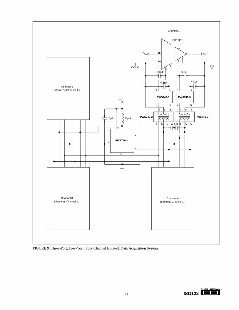
FIGURE 9. Three-Port, Low-Cost, Four-Channel Isolated, Data Acquisition System.
+V
Channel 2(Same as Channel 1.)
PWS740-1
4 65
33
4 4
0.3µF
ISO122P
0.3µF
0.3µF
64
1 1
66
16
15 7
0.3µF
Channel 1
1
Channel 4(Same as Channel 1.)
Channel 3(Same as Channel 1.)
98
2
VINV
OUT
123123
20µH PWS740-2 PWS740-2
50.3µF
10µF
6
3
4
8
5
10
PWS740-3 PWS740-3

12
®
ISO122
+15V
9
7
810
VIN , up to± 10V Swing
216
1–15
0.1µF0.1µF
0.33µF 0.33µF4
PWS740–3
VOUT
To PWS740–2,–1
NOTE: The input supplies can be subregulated to ±5V to reducePSR related errors without reducing the ±10V input range.
12
3
1
2
3MC78L05
+5VRegulator
–5VRegulatorMC79L05
VS
INPUT RANGE(V) (V)(1)
20+ –2 to +1015 –2 to +512 –2 to +2
FIGURE 10. Improved PSR Using External Regulator.
FIGURE 11. Single Supply Operation of the ISO122P Isolation Amplifier. For additional information see AB-009.
NOTE: Since the amplifier is unity gain, the inputrange is also the output range. The output can go to–2V since the output section of the ISO amp operatesfrom dual supplies.
ISO122P
R1 R2
R4
INA105Difference Amp
R3
RS
2
3
4
IN46895.1V
Reference
5
7
6
1VIN
Signal Source
+
NOTE: (1) Select to match R .S
10kΩ
15 1
9
V (+15V)S1
+V (+15V)S2
–V (–15V)S2
162
–VS1
Com 2
V = VOUT IN7
8
10
In
Gnd
ISO122
RC(1)
ISO122P
ISO122P

13
®
ISO122
15 16
1 2
10 9
ISO122P INPUT
SECTION OUTPUT SECTION
7 8
Gnd VIN V– V+
V+ V– VO Gnd
HPR117
6 5 4 2 1
Output Gnd
VO
VIN
+15V
–15V
Auxiliary Isolated Power Output
–15V, 20mA
+15V, 20mA Input Gnd
–15V, 20mA
+15V, 20mA
15 16
1 2
10 9
ISO122P INPUT
SECTION OUTPUT SECTION
7 8
Gnd VIN V– V+
V+ V– VO Gnd
HPR117
4 5 6 1 2
VIN
Input Gnd
+15V, 20mA
–15V, 20mA
Auxiliary Isolated Power Output
HPR117
6 5 4 1
VO
Output Gnd
Auxiliary Isolated Power Output
Gnd +15V
2
FIGURE 13. Powered ISO Amp with Three-Port Isolation. For additional information refer to AB-024.
FIGURE 12. Input-Side Powered ISO Amp. For additional information refer to AB-024.
IMPORTANT NOTICE
Texas Instruments and its subsidiaries (TI) reserve the right to make changes to their products or to discontinueany product or service without notice, and advise customers to obtain the latest version of relevant informationto verify, before placing orders, that information being relied on is current and complete. All products are soldsubject to the terms and conditions of sale supplied at the time of order acknowledgment, including thosepertaining to warranty, patent infringement, and limitation of liability.
TI warrants performance of its semiconductor products to the specifications applicable at the time of sale inaccordance with TI’s standard warranty. Testing and other quality control techniques are utilized to the extentTI deems necessary to support this warranty. Specific testing of all parameters of each device is not necessarilyperformed, except those mandated by government requirements.
Customers are responsible for their applications using TI components.
In order to minimize risks associated with the customer’s applications, adequate design and operatingsafeguards must be provided by the customer to minimize inherent or procedural hazards.
TI assumes no liability for applications assistance or customer product design. TI does not warrant or representthat any license, either express or implied, is granted under any patent right, copyright, mask work right, or otherintellectual property right of TI covering or relating to any combination, machine, or process in which suchsemiconductor products or services might be or are used. TI’s publication of information regarding any thirdparty’s products or services does not constitute TI’s approval, warranty or endorsement thereof.
Copyright 2000, Texas Instruments Incorporated