Investigations on Reconfigurable Dual Frequency Microstrip...
44
INVESTIGATIONS DN REDDNFIGUBABLE DUAL FREDUENCY MICRDSTRIP ANTENNAS USING VARACTDR DIDDES Contents 5.1 52 5.3 5.4 5.5 I5/§?3'§'5 ‘I/aractor C0ntmHkJ5ing@ Sbt firm L0adE:d'Rec01gfigwa5lIe 0)ua[ Trequency 9Vlr'cm.vtripflntemm 5. L1 5.1.2 5.1.3 5.1.4 5.1.5 ‘Frequency ‘Tuning "Variation qf(Duaf<R¢sonant ‘Frequendes 'wz'tfi ‘I/Z1 ractor Gipcerse =B2'a.§ jfintenna S132 ‘R¢¢fucti0n Szuafy qlfze Resonant<Befia1.-1brqftfie,?Intenmz at \Dj_$‘erent ‘I 'i1ractor¢Posi£ior1s (P0lZm':at1'0n, Qfain and'Q(ufati0n (Pattern Computation qf ‘Resonant ‘Frequencies qf “Varactor Tuned Qgcon_figwn6lZ: Antenna ‘I/aractor C0ntr0[!éJ dE (Dua[ ‘Frequemy flntenna (Des-ign_firr€l~"requem.y Ratio Tuning 5.3.1 flnterma Qeometry 5.3.2 5.3.3 ‘I/Zznlztimz qfflgsonant -Frequencies wizfi ‘I/i1rartor\'R¢uerse ifizkzs <P0£'1n'zati0n aru{§‘az'n 'E1qvr:'men!aI I rrvestigatiom on ‘I/amctor Loaded q{ecor9‘igura6&: fliicmstrip }Ir1termasforQZr|!iaru:eJ<1)ua[q~‘requen¢) ‘Tuning amfflrea <KeJuct1'on 5.4. I 5.4.2 5.4.3 5.4.4 ‘I/Zirartor (,bntr0!II2d'f3/!1'(r0stn'pjIntenna -win? <'l)ua[OrI/z<>é;0na{.5T0t,‘/Imzs Tripfi: Sfiwt /"Inn Loazfezf qlecorgfigurafié ~’Dua[ Trequeng ;'1ficrosm'p jqntenna ‘Using "I/Izractors ‘F-0ur_S‘IZ)tj?Inn Loaded’!/bmrtor (‘ontrol1Z2J%cory‘Igun16fi:fwicrostnpjlnterma ‘Eigfit.S'£>t /‘lmz L0aJe¢f’(/aractor (,‘0"ntmlZ:J*R¢c0qfi;;ura6[c' i11r'crostn'p fintenna I Trequmqy ‘Ewing in .?[ex_agonaIS£>t Loadkz{9Hz'cr0stn'p/'lntem1a ‘Using 9/!0d§fieJ.S'lbtjIrm 5. 5.1 C'-.ST1apc¢f.S'[0t [.0a<feJ~1{gconfigura6[c £1/f11"rostn'p,1-Intenmz 5.5.2 §I1canJcrc¢{.S'{0£ /Irm Loafeaf Q"(gc0n_f|;_gura5(e £T1r'cros1‘r1'p _.9Intcmu1 142 I43 I44 146 I46 I47 I50 153 I53 154 I56 54 160 I64 I67 J71 176 .176 I81
Transcript of Investigations on Reconfigurable Dual Frequency Microstrip...
INVESTIGATIONS DN REDDNFIGUBABLE DUAL
FREDUENCY MICRDSTRIP ANTENNAS USING
VARACTDR DIDDES
Contents
5.1
52
5.3
5.4
5.5
I5/§?3'§'5
‘I/aractor C0ntmHkJ5ing@ Sbt firm L0adE:d'Rec01gfigwa5lIe 0)ua[ Trequency9Vlr'cm.vtripflntemm
5. L1
5.1.2
5.1.3
5.1.4
5.1.5
‘Frequency ‘Tuning
"Variation qf(Duaf<R¢sonant ‘Frequendes 'wz'tfi ‘I/Z1 ractor Gipcerse =B2'a.§
jfintenna S132 ‘R¢¢fucti0n
Szuafy qlfze Resonant<Befia1.-1brqftfie,?Intenmz at \Dj_$‘erent ‘I 'i1ractor¢Posi£ior1s
(P0lZm':at1'0n, Qfain and'Q(ufati0n (Pattern
Computation qf ‘Resonant ‘Frequencies qf “Varactor Tuned Qgcon_figwn6lZ:Antenna
‘I/aractor C0ntr0[!éJ dE (Dua[ ‘Frequemy flntenna(Des-ign_firr€l~"requem.y Ratio Tuning
5.3.1 flnterma Qeometry5.3.2
5.3.3‘I/Zznlztimz qfflgsonant -Frequencies wizfi ‘I/i1rartor\'R¢uerse ifizkzs
<P0£'1n'zati0n aru{§‘az'n
'E1qvr:'men!aI I rrvestigatiom on ‘I/amctor Loaded q{ecor9‘igura6&: fliicmstrip
}Ir1termasforQZr|!iaru:eJ<1)ua[q~‘requen¢) ‘Tuning amfflrea <KeJuct1'on
5.4. I
5.4.2
5.4.3
5.4.4
‘I/Zirartor (,bntr0!II2d'f3/!1'(r0stn'pjIntenna -win? <'l)ua[OrI/z<>é;0na{.5T0t,‘/Imzs
Tripfi: Sfiwt /"Inn Loazfezf qlecorgfigurafié ~’Dua[ Trequeng ;'1ficrosm'p jqntenna
‘Using "I/Izractors
‘F-0ur_S‘IZ)tj?Inn Loaded’!/bmrtor (‘ontrol1Z2J%cory‘Igun16fi:fwicrostnpjlnterma
‘Eigfit.S'£>t /‘lmz L0aJe¢f’(/aractor (,‘0"ntmlZ:J*R¢c0qfi;;ura6[c' i11r'crostn'p fintenna
I Trequmqy ‘Ewing in .?[ex_agonaIS£>t Loadkz{9Hz'cr0stn'p/'lntem1a‘Using 9/!0d§fieJ.S'lbtjIrm
5. 5.1 C'-.ST1apc¢f.S'[0t [.0a<feJ~1{gconfigura6[c £1/f11"rostn'p,1-Intenmz
5.5.2 §I1canJcrc¢{.S'{0£ /Irm Loafeaf Q"(gc0n_f|;_gura5(e £T1r'cros1‘r1'p _.9Intcmu1
142
I43
I44
146
I46I47
I50
153
I53154
I56
54
160
I64
I67
J71
176
.176
I81
one of the most important characteristics of frequency reconfigurable
antennas is their flexibility in operation. That is, one can easily control their
operating frequencies by simply selecting the desired 6X[€IT12ll bias and without
bothering about the antenna dimensions. Even though the PIN diode
controlled reconfigurable antenna scheme described in the earlier section
permits this, a n_r9,re_ flexible frequency tuning scheme can beaccomplished by‘replacing the PIN diodes with Varactor diodes.
Here Varactors are integrated with the extended slot ann of the dual frequency
microstrip patch antenna. The Varactors provides various capacitive loadings to
the microstrip patch. The Varactor junction capacitance varies against the bias
voltage and can be calculated from the applied bias voltage as,
C I ._£L__.. (5-1)@_V%J’
where, CO is the Varactor capacitance at OV DC bias, V is the applied bias
voltage which is —ve for reverse bias, V,,, is the built—in potential and y is a
constant depending on the doping profile of the p-n junction [185]. The
capacitance value can be decreased by reverse biasing the Varactor diode. These
different capacitance loadings correspond to various electrical lengths of the
protruding slot arm, thus giving different resonant frequencies. This dual
frequency tuning scheme provides fast tuning over a wide frequency range, as is
required for many applications. The various designs intended for both
reconfigurable dual frequency operation and frequency ratio tuning are
presented in detail.
14
C /Jqvter -5
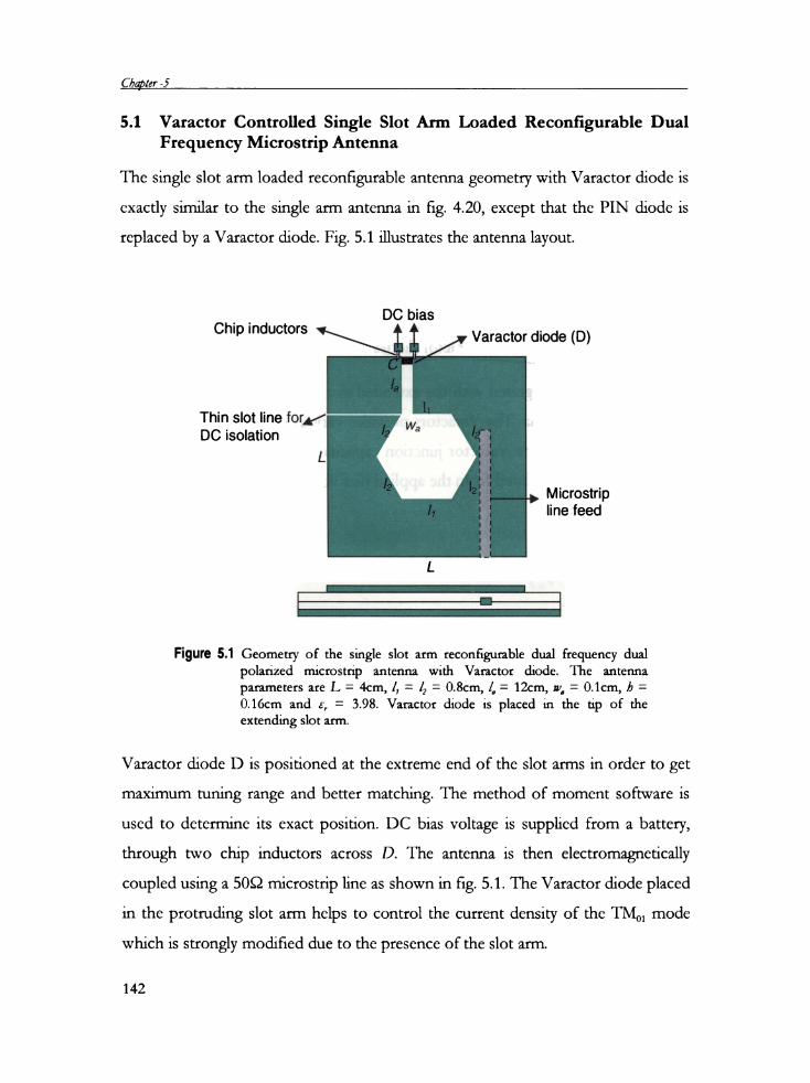
5.1 Varactor Controlled Single Slot Arm Loaded Reconfigurable DualFrequency Microstrip Antenna
The single slot arm loaded reconfigurable antenna geometry with Varactor diode is
exactly similar to the single arm antenna in fig. 4.20, except that the PIN diode is
replaced by a Varactor diode. Fig. 5.1 illustrates the antenna layout.
_ _ DC biasChm mductors ‘g f l , Varactor diode (D)
Thin slot line for4/DC isolation
L
+ Microstripline feed
Figure 5.1 Geometry of the single slot arm reconfigurable dual frequency dualpolarized microstrip antenna with Varactor diode. The antennaparameters are L I 4cm, I, = /2 I O.8cm, I, = 12cm, 221, = O.1cm, /J =O.16cm and 5, = 3.98. Varactor diode is placed in the tip of theextending slot arm.
Varactor diode D is positioned at the extreme end of the slot arms in order to get
maximum tuning range and better matching. The method of moment software is
used to determine its exact position. DC bias voltage is supplied from a battery,
through two chip inductors across D. The antenna is then electromagnetically
coupled using a SOQ microstrip line as shown in fig. 5.1. The Varactor diode placed
in the protruding slot arm helps to control the current density of the TM0, mode
which is strongly modified due to the presence of the slot arm.
142
Ir:z1e.¢tQ{ati0rLs0n9(;r0nfl{gura6l2: 1)ua[fFrequeru:yMzi:rast1ipJ4ntzrmasu.n3g1/aract0r1)zbd2.s
Varactor embedded in the protruding slot arm provides various capacitive loadings
across the slot arms in different reverse bias conditions. The junction capacitance
of the Varactor varies against the reverse bias voltage applied and these different
capacitive loadings correspond to different electrical lengths and thus different
resonant frequencies.
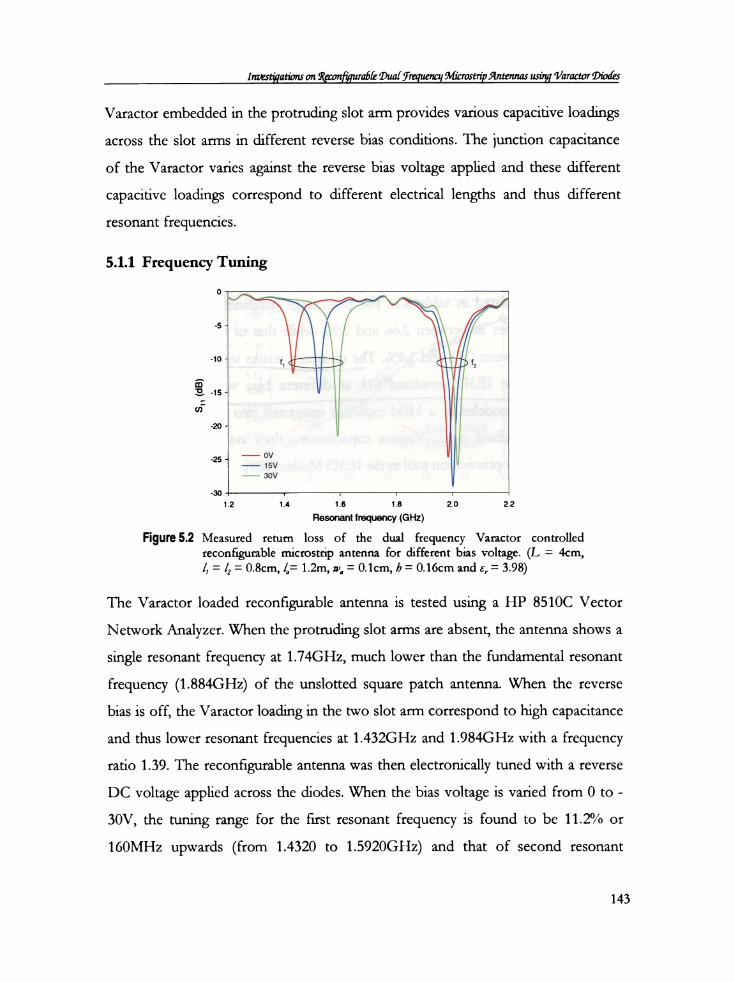
5.1.1 Frequency Tuning0 1 *;*-’ o 1». A / ff e t t a- _5 ~l . , , c ,| ‘A l“ *'
1
l'10 f‘ ’ fzEa‘ T of'3 -1s~:2 " licn it'1 .-20- 4’ Il_25_ —ov l‘:15V1 30V ''30 '1 I I 1 I1.2 1.4 1.6 1.8 2.0 2.2
Resonant frequency (GHz)
Figure 5.2 Measured return loss of the dual frequency Varactor controlledreconfigurable microstrip antenna for different bias voltage. (L = 4cm,/, = /2 I O.8cm, /,= 1.2m, av, = O.1cm, /J = O.16cm and 6, = 3.98)
The Varactor loaded reconfigurable antenna is tested using a HP 8510C Vector
Network Analyzer. \X/hen the protruding slot arms are absent, the antenna shows a
single resonant frequency at 1.74GHz, much lower than the fundamental resonant
frequency (1.884GHz) of the unslotted square patch antenna. When the reverse
bias is off, the Varactor loading in the two slot arm correspond to high capacitance
and thus lower resonant frequencies at 1.432GHz and 1.984GHz with a frequency
ratio 1.39. The reconfigurable antenna was then electronically tuned with a reverse
DC voltage applied across the diodes. When the bias voltage is varied from O to
30V, the tuning range for the first resonant frequency is found to be 11.2% or
160MHz upwards (from 1.4320 to 1.592OGHz) and that of second resonant
143
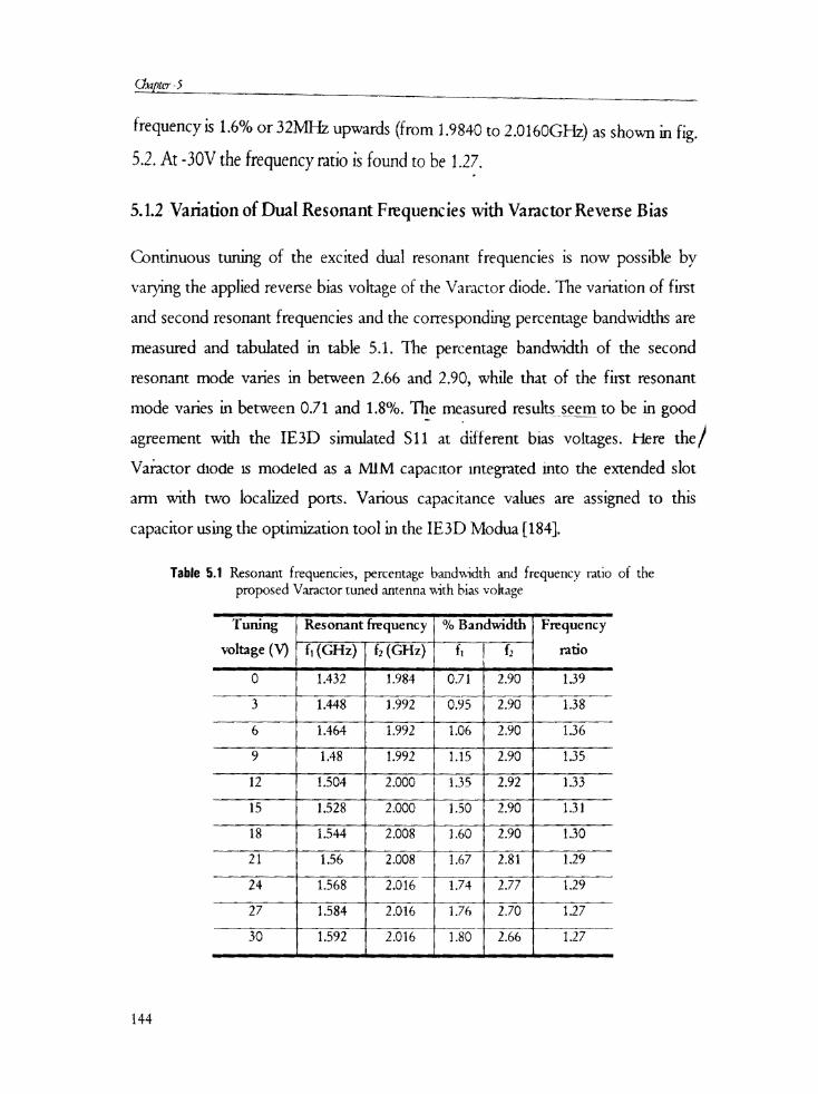
77 7 7 7 7 _frequency is 1.6% or 32MHz upwards (from 1.9840 to 2.016OGHz) as shown in fig.
5.2. At -30V the frequency ratio is found to be 1.27.I
5.1.2 -Variation of Dual Resonant Frequencies with Vamctor Reverse Bias
Continuous tuning of the excited dual resonant frequencies is now possible by
varying the applied reverse bias voltage of the Varactor diode. The variation of first
and second resonant frequencies and the corresponding percentage bandwidths are
measured and tabulated in table 5.1. The percentage bandwidth of the second
resonant mode varies in between 2.66 and 2.90, while that of the first resonant
mode varies in between 0.71 and 1.8%. The measured results seem to be in goodIr r
agreement with the IE3D simulated S11 at different bias voltages. Here the
Vaiactor diode 1S modeled as a Nl1M capacitor integrated into the extended slot
ann with two localized ports. Various capacitance values are assigned to this
capacitor using the optimization tool in the IE 3D Modua [184].
Table 5.1 Resonant frequencies, percentage bandwidth and frequency ratio of theproposed Varactor tuned antenna with bias voltage
Tuning ,1 Resonant frequency % Bandwidth f Frequencyvoltage f1T((9;H2)T. (élrlizlff fr if f; ll ratio
— —7~7~7 ~7.7'.—7—7—7—7‘7 7,7 7 7 .7 7 7 — 7 7 77 70 1 1.452 1. 1.984 ‘ 2.90 . 1.5911
DJ
7.1-7i—l
O0
h-L
‘so\Ol\J
.0\Jii74777 7774-7
7 7777
L7l
— 7 : é 7 ~i 7 7 7 7 7. : : 774 7,7 7_— —; 7 74 7— —7 7 7 7 7 70.95 2.90 1 1.38777.777 7117.77 777777777776 A 1.464 1992 F 1.06 2.90 j 1.361 .
H.I\.J
l
17 717 71771
'0‘ 1OIO1 171177.7 71
b-if i—A1.,» 2-.»um U1
P.\01r\.>
I
I-—\
wan
7.77.1777. 77.7 7W77777— — +7 — '7 <— 7 — . 7 — '7 '7 7 77 77'9 ‘ 1.48 1 1.992 2.90 4 1.35
1504 A 2 9— — — 7 7 7 *7 7 77 7 — 7 7 7, 7 7 7 7 71‘ 15‘ 9* 1.528 2.000 *1.50“72.90. 91.31‘
” 1.90 if 2.90‘ 1.50
/7
77 7 7 .l7 7 7 71 77 77 7 7 7 7 7 7 7 7 7 77 7 17 7 7 7 7 7 7 7 718 1 1.544 y 2.008 8 A at
7.7l 7)-all
5*\-I
T”Xr-A
1-»|\-J\O
i 7% *7 7 7 777'-l 7 7 '7 77 7 77 7 ‘l * 7 *. 7 7 77 ‘7 7 7 7 7 7_ 77 U21 ;. 1.58 1 2.008 A24 1.588 2.018 1‘ 1.7i4‘i1‘2.72T[ 1.29‘ J
77 7|. _
7 7 7 7 7 7 1 7 .7 7 7 _ 7 .. _ 7 7 7~ — 7‘ 7 7 77177 77 7— L177 7 7 7.. 7 7 7 7 7
27 T 1.584 2.018 1 1.78 N. 2.70 1.277- 77 77 ,7 7 7 7 777777771777717777750 ta 1.592 1 2.018 1 1.80“ 2.88 1.27
’7‘7’7i 7777779777’ 7‘li'777 7 i _—7*7.77 '7 '77 77 77. 777777
144
Imwtyahbm an Rgconfiyurabk 1)ua[fFreq‘ue11cy Micrartvipfllntzmms ‘Varactvr Drbdks
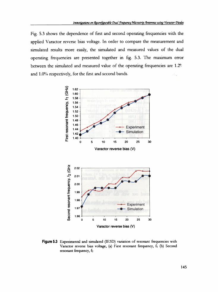
Fig. 5.3 shows the dependence of first and second operating frequencies with the
applied Varactor reverse bias voltage. In order to compare the measurement and
simulated results more easily, the simulated and measured values of the dual
operating frequencies are presented together in fig. 5.3. The maximum error
between the simulated and measured value of the operating frequencies are 1.29
and 1.0% respectively, for the first and second bands. ,
(GHz)
162*L501L58 *
1.56 7L54L52—
1.50 —
143"1.46 - _1 —--— Experiment44142 -0- Simulation0_ 1f I ~ l I I I IO 5 10 15 20 25 30
t resonant frequency, t1F'rs
Varactor reverse bias (V)
72 (GHz
202
201
cy,
200*
equen
L99~
Second resonant fr
L98
—~— Experiment‘-97 -0- Simulation1,96 1‘ 7' f i i I I 1O 5 10 15 20 25 30
Varactor reverse bias (V)
Figure 5.3 Experimental and simulated (IE3D) variation of resonant frequencies withVaractor reverse bias voltage, (a) First resonant frequency, f1 Secondresonant frequency, fg
145
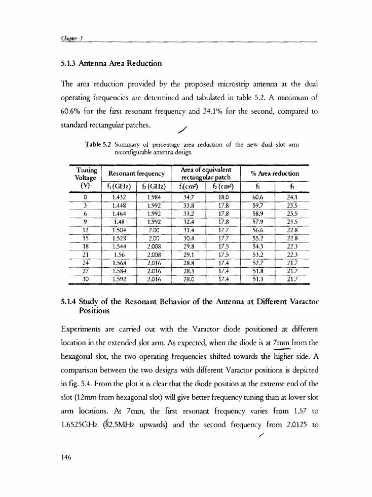
O”P'£?f5 _5.1.3 Antenna Area Reduction
The area reduction provided by the proposed microstrip antenna at the dual
operating frequencies are determined and tabulated in table 5.2. A maximum of
60.6% for the first resonant frequency and 24.1% for the second, compared to
standard rectangular patches. /
Table 5.2 Summary of percentage area reduction of the new dual slot armreconfigurable antenna design
iuningi R R Area of equivalent i R .Voltage Resonant frequency mctangularpatch 9 % Area reduction
(v)9 . f1(GHz) f;(GHz)l 1,(¢m1) 1.(¢m1) A 1.2 1.9 9 9 24.1__ .1 _M 0 21.432 1.9842 34.7 18.0 1*“ 60.6 ‘Ti39 Z 1.448___ __ 1 1992 333 ML
.29. 2356 1.464 1.992 33.2 23.5A 21.48 1.992 32A _i l 2359
1.50412 1 2.00 ‘L 31A 22315 ‘ L528 2.00 30A
1
1
l
22318 » L544. .l_ -_
1
2.003l?_
29.3 _Y 22.3
21 1.56 2008 2917
22.3
924 9 1.5698 2016 283 !
l 2L727 1 ” 1.584 2.016 283
1
21.7
30 1.592 2.016 1 28.0 1 17.4 l 51.3 19 9 9_ 9 99 9 21]5.1.4 Study of the Resonant Behavior of the Antenna at Different Varactor
Positions
Experiments are carried out with the Varactor diode positioned at different
location in the extended slot ann. As expected, when the diode is at 7mm from the
hexagonal slot, the two operating frequencies shifted towards the higher side. A
comparison between the two designs with different Varactor positions is depicted
in fig. 5.4. From the plot it is clear that the diode position at the extreme end of the
slot (12mm from hexagonal slot) will give better frequency tuning than at lower slot
ami locations. At 7mm, the first resonant frequency varies from 1.57 to
1.6525GHz (§2.5MHz upwards) and the second frequency from 2.0125 to/146
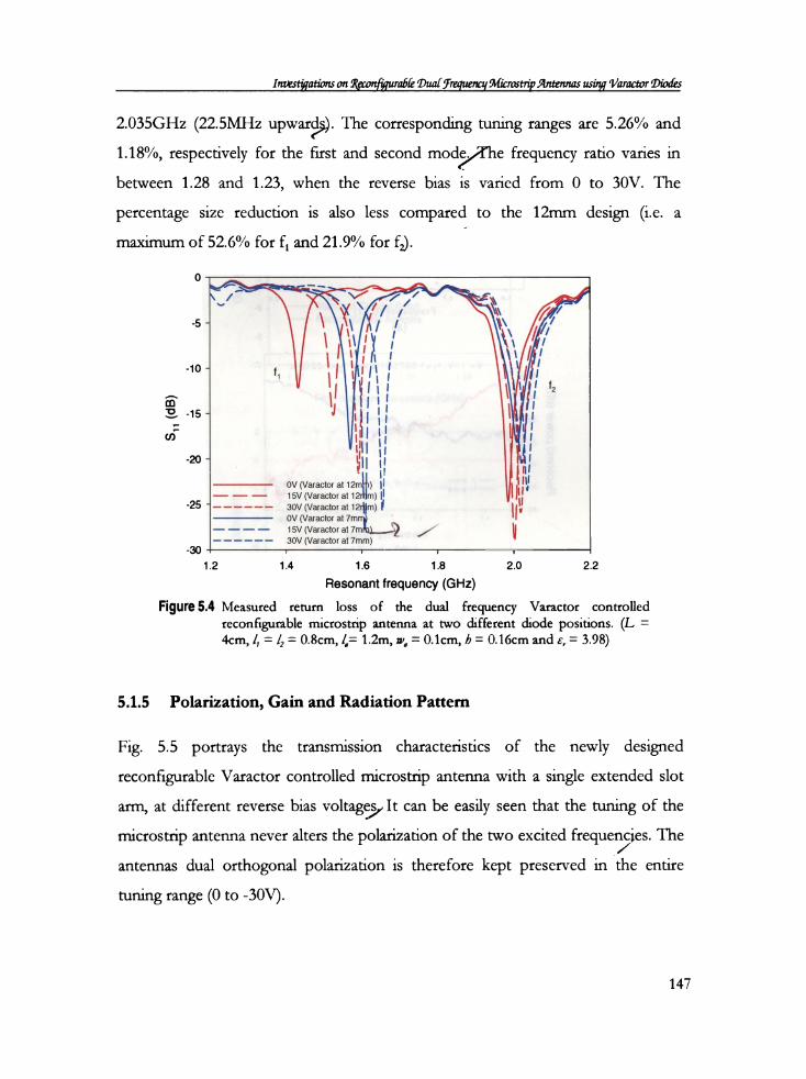
Inwst1'gaflbmm§(pcmifig14ra6[eDuaI9'mqz4amyM1tr0stflpJ1r1tz1mas zm'1g’l/aractvrlhbés
2.035GHz (22.5MHz upwar§). The corresponding tuning ranges are 5.26% and
1.18%, respectively for the first and second mode/The frequency ratio varies inbetween 1.28 and 1.23, when the reverse bias is varied from O to 30V. The
percentage size reduction is also less compared to the 12mm design (i.e. a
maximum of 52.6% for f, and 21.9% for f2).4'l it / Z//
O
(\
A A J—‘<___--I';"’}___ /_r_4 *3.4____.—\-~{* \__ \
___‘\
\\ . / ii-s — \ \\ //l \\\ /l ‘ ,'-10 - t1 ‘ I pl,
jg -15 - i+ ‘i.l|:l M
_ g _ ‘pr-'_.?-Qt» ‘&;:?4 4‘_‘ rgfli-1
‘SQ
I I .(D .-20- M AA.
in
—-i— 0V(Varactorat12mb) l— -— —- 15V (Varactorat 12 m)'25 " ———— —— 30V (Varactor at 12 m) I
Z——-L OV (Varactor at 7mri-"g ‘ ‘— — — — 15V (Varactor at 7m Q / N———— — — 30V (Varactor at 7mm)-30 -1 n i I I |1.2 1.4 1.6 1.8 2.0 2.2
Resonant frequency (GHz)
Figure 5.4 Measured return loss of the dual frequency Varactor controlledreconfigurable microstrip antenna at two different diode positions. (L =4cm, l, = /2 = O.8cm, /,= 1.2m, 2:1, = O.1cm, /2 = O.16cm and 6, = 3.98)
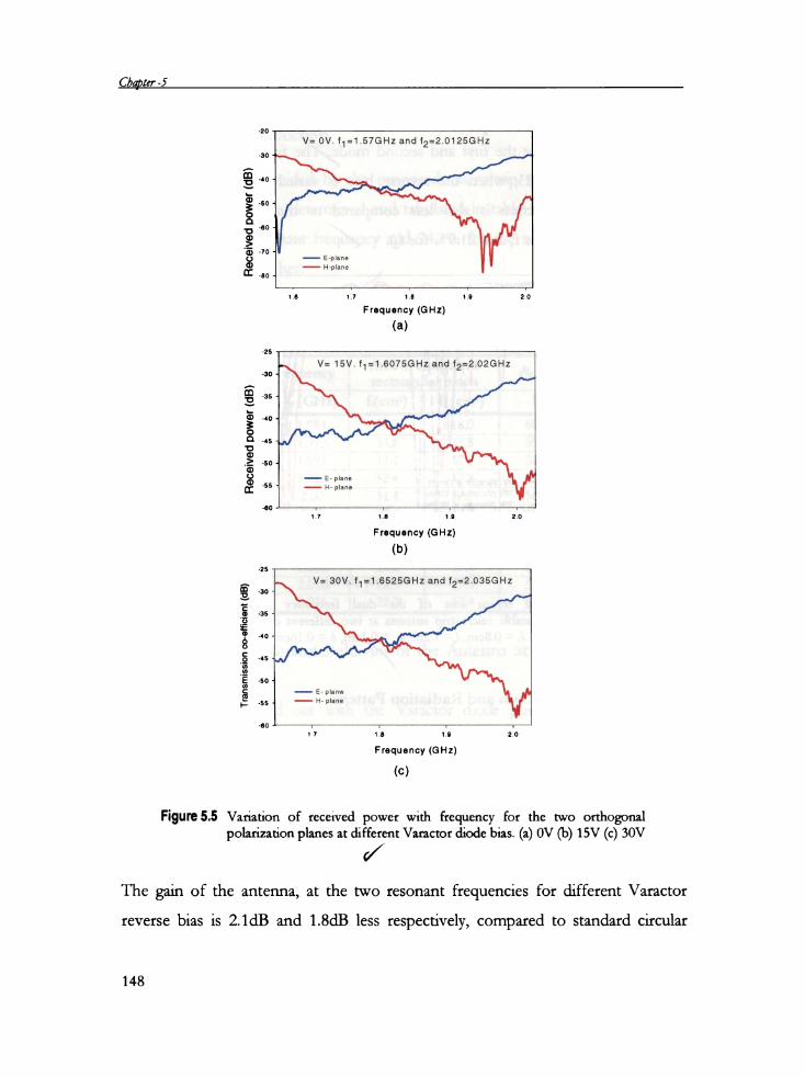
5.1.5 Polarization, Gain and Radiation Pattern
Fig. 5.5 portrays the transmission characteristics of the newly designed
reconfigurable Varactor controlled microstrip antenna with a single extended slot
arm, at different reverse bias voltages, It can be easily seen that the tuning of the
microstrip antenna never alters the polarization of the two excited frequerfiies. Theantennas dual orthogonal polarization is therefore kept preserved in the entire
tuning range (O to -30V).
147
Chapter -5
Hece ved Dower (dB)Rece ved power (dB)
-1
F
dB
§ri1.
s on co-eIfc'enTransm s
25
30
35
40
45
50
55 <
20
30
5O
UlO
OO
QO
QO
25
-so
-as
-40
DU\
-so
-ss
-co
V= OV. f1=1.57GHZ and f2=2.O125GHZ
i E-planei H~pIane1 r 1 016 1.7 1.3 19 20
Frequency (GHZ)
(a)
c
-1'
V=15V.11=1.6O75GHZ and f2=2.O2GHZ
i E- planei H-plane V 1*7 i1.7 1.8 1.9 20
Frequency (GHz)
(b)
V= 30V. f1=1.6525GHZ and f2=2.O35GHZ
—— E» planw——- H-plane
60 — 1 r '1 —‘17 1.8 1.9 20Frequency (GHz)
(<1)
Figure 5.5 Variation of received power with frequency for the two orthogonalpolarization planes at different Varactor diode bias. (a) OV 15V (c) 30V
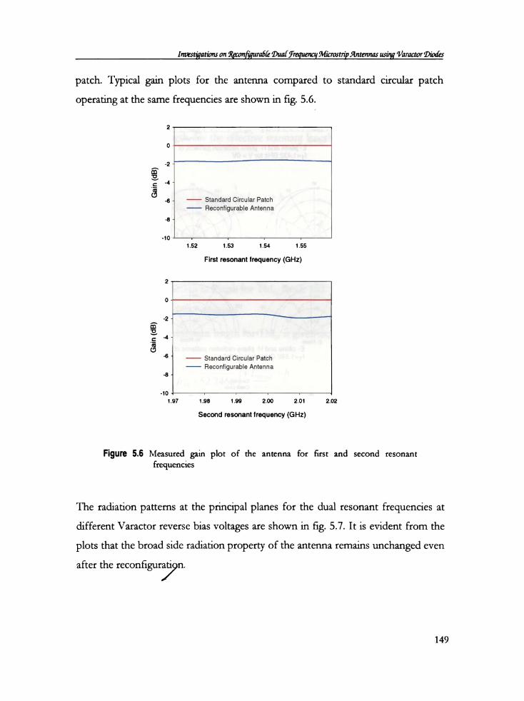
The of the antenna, at the two resonant frequencies for different Varactor
reverse bias is 2.1dB and 1.8dB less respectively, compared to standard circular
148
Imnvtymbruonflpmfigwafié 1)ua[,‘}'req‘uerra{Mi2:rart1'§v5/lntervms zrsr'1y‘l/aractvrflorfas
patch. Typical gain plots for the antenna compared to standard circular patch
operating at the same frequencies are shown in fig. 5.6.
2 .
O1.21 *
Ga'n (as)
-4-q
.5 - i Standard Circular Patchi Reconfigurable Antenna
.3'10 1 I I l1.52 1.53 1.54 1.55First resonant frequency (GHz)
2 .,
0..
-2.l
(<15)
.44
Ga'n
'6 ' — Standard Circular Patchi Reconfigurable Antenna
.8
‘1O '1 1 I l ' 11.97 1.98 1.99 2.00 2.01 2.02Second resonant frequency (GHz)
FlgUl‘6 5.5 Measured gain plot of the antenna for first and second resonantfrequencies
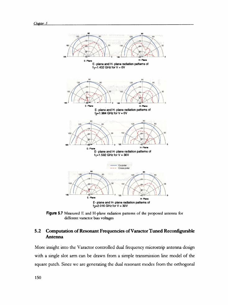
The radiation patterns at the principal planes for the dual resonant frequencies at
different Varactor reverse bias voltages are shown in fig. 5.7. It is evident from the
plots that the broad side radiation property of the antenna remains unchanged even
after the 1’€COI’1figl11‘?fl.
149
Cbqbter -5 90 90120 /./’ 60 129 \ 60\-—____\_ ‘ ' ‘,/ />14} * _____\ " \\\_//» ‘I / _ / ’ / \' 30 3/ /f::/ _ \ \\I.
1 kg‘/:29. ..________1, ll V‘ l 50 i -V -' / '_ /‘_‘w___\_\__‘>K V ‘E/:‘,_\,~ J, l \ / ' r /\ " t/ >1 r \ / "‘-la. /' L » ,' » \< w / ‘#1 -§D— +~~__ ~: \ 2 ’ " \';»' - " i ‘1 ~ \ 1 it|30 a_. . . . l O 180 ' 1 _'| _‘4\Q“:l‘."l:'“7 _L _ L 0E- Plane H‘ Pb”E- plane and H- plane radiation pattems oil1=1.432 GHz for V = 0V90 90120 ‘ '\\3O 120 * \ 60/ \ ’ ‘/ q ~ ~~_v-_V \ ~ >19 ~--__1' "~‘__ \\_\ l ,-="';" 717""-4'
150 c ~_____ , __:.\ 30 1.50 ‘ q 29_ _f 7"'\ 301' ”
/if ~¢*t;¥
q J\k
\ “ “v.
e‘>;i<i[tf
ii,
. f V. .e s ’ » ~ \ K \ l 1 \ /+_
i ll‘ I I‘ "1 ‘ i I‘,-‘Ii "1'/1 ‘ i It ___ V _ r_‘ ‘130 K ; -#- Q 1“) mi | ls OE- Plane H- PlaneE- plane and H- plane radiation pattems off2=1.984 GHz for V = 0V9Q 90120, “ - so 120 “Rio‘ \" JJQQ _______ ‘ . j__-.-1Q— —~.____w llf i;#'~ \\iv< // >f,-- w~t ‘\
150 20 7_____<g_§ s. x 30 150 Rx M/:29 _1\\{i\ A ’v>>_V_,\3O/ .- ;/ 3-\ - '~ _/', »I ,_ V, \_\ /_.\ I V. W) q 1 \l ‘i | ,3 "yin, Q ‘;-Jl‘->- \ l‘ ll Vl ‘ J “i‘~.___ I __,.-»~“'.: '\\ l ‘180 L _ l iii“ l‘ i _. 0 180 ilk l iv ix“ /i mm‘ OE- Plane H' mam
E- plane and H- plane radiation pattems oft1=1.592 GHz lor V = 30V
i Co-polar— — - Cross-polar
90 eo12° ‘\~. 5° 120 so/. ‘ ‘ ‘ l/' I _ _:-19 ‘ '“—~-____>\ \\__ f_,_jQ L ____7_ \"_/‘ '_Y-‘* " 1» ~150 /“ -. _ " i \~ / < I -~ ' \/-~._‘ .> ‘.',;2g“* ~~__\‘_. ____/\'\\ A -p :20 7_r¢_“‘ \»\ / \ ~ a = / i r -4 ~» - \qty ‘\ /' “j/ii, / M '~ \ t._.‘ , I, l‘ ‘ \___ q \
’) we no . =1 v 0E- Plane H_ HamE- plane and H- plane radiation pattems ofl2=2.016 GHz for V = 30V
\'w<l.,/la/>alg. 1. \
,><.g 2
Figure 5.7 Measured E and H-plane radiation patterns of the proposed antenna fordifferent varactor bias voltages
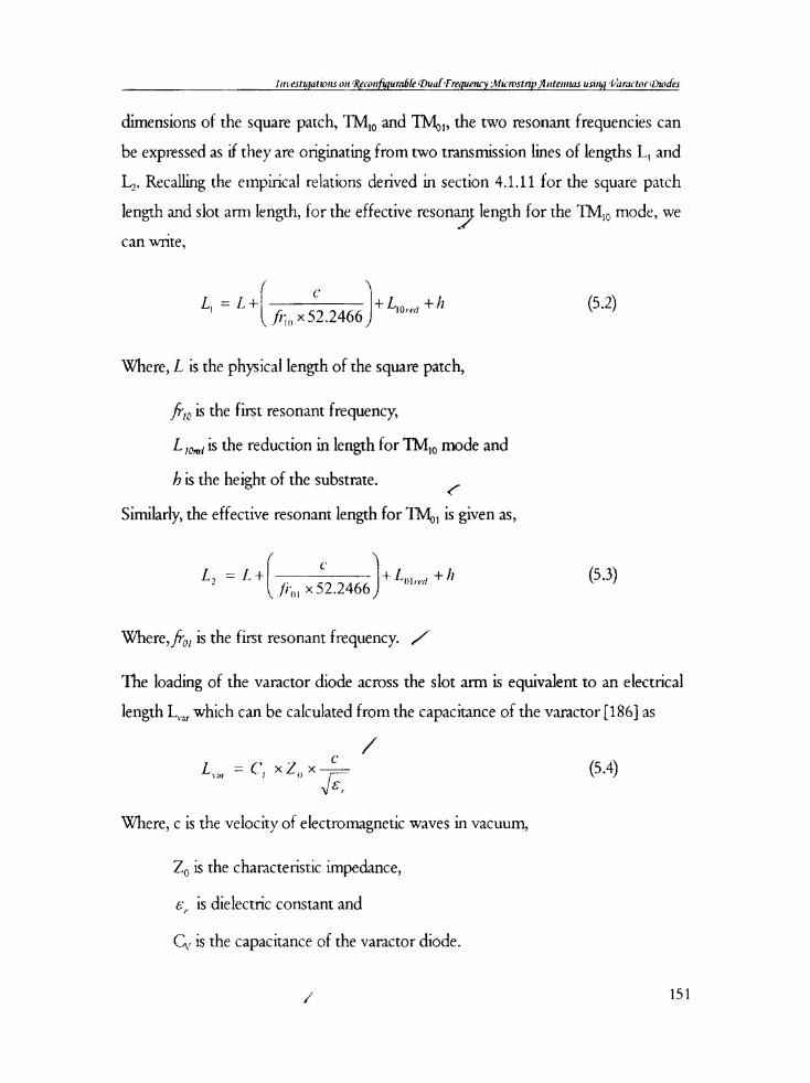
5.2 Computation of Resonant Frequencies of Varactor Tuned ReconfigurableAntenna
More insight into the Varactor controlled dual frequency microstrip antenna design
with a single slot arm can be drawn from a simple transmission line model of the
square patch. Since we are generating the dual resonant modes from the orthogonal
150
__ __ g g WW 1-m=e.tt;'gatz'o:i.s on _{1Z;;q@fi§g1_rg6{i2 ~’Duaf 'Fr;{q:ggr_:Q1 I/1/fl'(_fD.$Ifl'P/"lllIBlI'!1(l$ um; "f/i1__!'d(lO!_'ilg2-(_T_dé‘,i
dimensions of the square patch, TM“, and TMM, the two resonant frequencies can
be expressed as if they are originating from two transmission lines of lengths L, and
L2. Recalling the empincal relations derived in section 4.1.11 for the square patch
length and slot arm length, for the effective resonagt length for the TMN, mode, wecan write,
C
L, = 1. +[ gfigm-152.2466 J + 1.10,, d + h (5.2)
Where, L is the physical length of the square patch,
fr“, is the first resonant frequency,
L mm, is the reduction in length for TM“, mode and
/9 is the height of the substrate. KSimilarly, the effective resonant length for TNI01 is given as,
U
L, = 1.+ _ ,9-3-; +L,,,m, +1: (5.3)‘ frm ><52.Z466
Where, fio, is the first resonant frequency. /i
The loading of the varactor diode across the slot ann is equivalent to an electrical
length Lm which can be calculated from the capacitance of the varactor [186] as
. C /Lvar : X Z0 X F_\X/here, c is the velocity of electromagnetic waves in vacuum,
Z0 is the characteristic impedance,
5,. is dielectric constant and
CV is the capacitance of the varactor diode./' 151
Q’“!?“3Tf5 o__ _ *7 _. -_ 1 s sAs the varactor junction capacitance varies with the applied reverse bias voltage
VI“, we can express C\.- in tenns of Vm, as,
'1CI Z c‘.'._...__, (5-5)( ‘ w 1,...-mi\ I/iii . ‘Z
Where, Q is the varactor junction capacitance at zero bias voltage,
Vb, is the built in potential for the semiconductor matenal used in thevaractor and
/‘
y is a constant depending on the doping profile of the varactor p-n junction.
Assuming that the varactor loading affects only the first resonant mode, we can
modify the effective electrical length of the TM“, mode as,
1K C \ (.',, c lL, I .- ——----- ——- l+ L|,,,_‘_d + /I + -- >< Z‘, >< -._-.;.. !
, f1"... >< 52.2466 , 1.» i" \;t-,I.» i~ I 1 l\ .':
Knowing L, and L2 we can calculate the corresponding dual resonant frequencies
for the varactor loaded reconfigmble patch antenna as,
First resonant frequency = e-—- L-_:-_+-._- afld (5-7)2 L I '\'I grefli
.. /Second resonant frequency = C. -: (5-8)
2 L_, \,,!s,_€fl, /The comparison of experimental and theoretical results for the single slot arm
loaded varactor controlled reconfigurable dual frequency microstiip antenna is
given in fig.5.8. /152
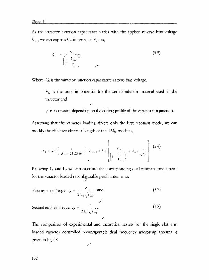
Irwest'gat1'oris on Rgconflurafik 1)ua[1Treq‘uenci{ fllntiennas ‘I/aractvr 1)i'0ifl's
2.2 ~I-\
equency GHz
V 2.0- * ‘-—¢i f2, Experimental
1.8 ' _ -ii. - f2, Theoreticali0—— f,, Experimental
Resonant fr
1_5 - — —I — f,, Theoreticalg I“ l i I l l 1 . -1
O 5 10 15 20 25 30 35
1.4
Varactor reverse voltage (V)
Figure 5.8 Plot showing the experimental and theoretical variation of first andsecond resonant frequencies with the applied varactor reverse bias
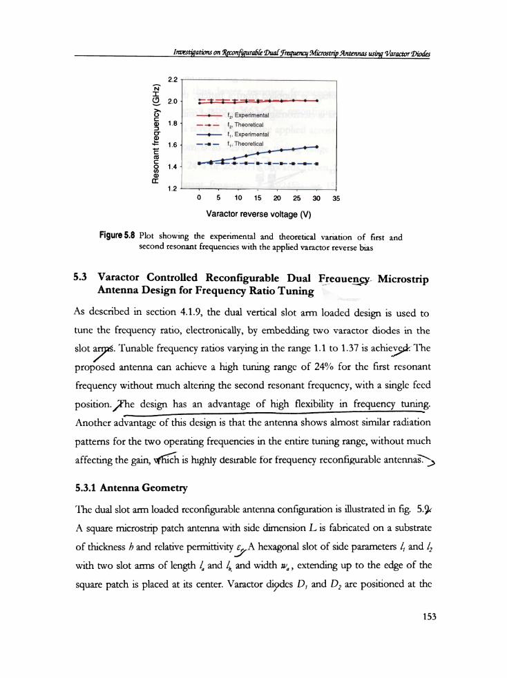
5.3 Varactor Controlled Reconfigurable Dual Freaueggz» MicrostripAntenna Design for Frequency Ratio Tuning T
As described in section 4.1.9, the dual vertical slot arm loaded design is used to
tune the frequency ratio, electronically, by embedding two varactor diodes in the
slot 2?-§. Tunable frequency ratios varying in the range 1.1 to 1.37 is achie'§d<' Theproposed antenna can achieve a high tuning range of 24% for the first resonant
frequency without much altering the second resonant frequency, with a single feed
position. jhe design has an advantage of high flexibility in frequency tuning.
Another advantage of this design is that the antenna shows almost similar radiation
patterns for the two operating frequencies in the entire tuning range, without much
affecting the gain, is highly desirable for frequency reconfigurable antennas.\)
5.3.1 Antenna Geometry
The dual slot arm loaded reconfigurable antenna configuration is illustrated in fig. 5.‘)<"
A square microstrip patch antenna with side dimension L is fabricated on a substrate
of thickness /2 and relative pennittivity-e]A hexagonal slot of side parameters /, and /2
with two slot arms of length /,, and /,,, and width 22/, , extending up to the edge of the
square patch is placed at its center. Varactor diodes D, and D2 are positioned at the
153
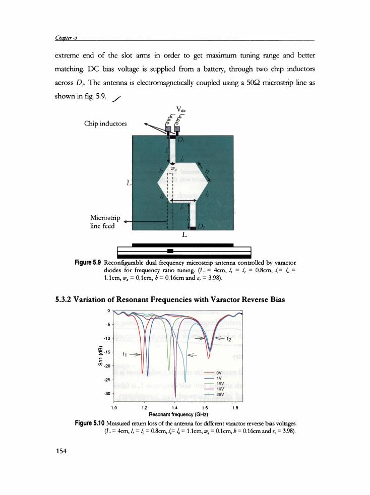
Cbqbter -5
extreme end of the slot aims in order to get maximum tuning range and better
matching. DC bias voltage is supplied from a battery, through two chip inductors
across D,. The antenna is electromagnetically coupled using a 5052 microstrip line as
shown in fig. 5.9. /Vdc
Chip inductors K {£
L
Microstrip ‘_line feed ;L
Figure 5.9 Reconfigurable dual frequency microstrip antenna controlled by varactordiodes for frequency ratio tuning. (I. I 4cm, l, I I, I O.8cm, /‘I I, I1.1cm, 12/, I O.1cm, /2 I O.16cm and 5, I 3.98).
5.3.2 Variation of Resonant Frequencies with Varactor Reverse Bias0
-5l-10 ' l € f2
‘” -20 R H l ——ov-25 R l —— igv— 19v-3° ~ — 29vI 1 I I I1.0 1.2 1.4 1.6 1.8
Resonant frequency (GHz)
Figure 5.10 Measured retum loss of the antenna for different vamctor reverse bias voltages.(I. I 4cm, /, I /2 I O.8crn, /,,I 1,, I 1.1cm, wa I O.1cm, /2 I O.16cm and 5, I 3.98).
154
Inw.¢t@]at1'on.s on fipconfgurafik ‘Varactor Diodks
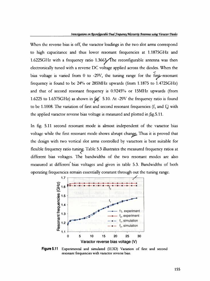
When the reverse bias is off, the varactor loadings in the two slot arms correspond
to high capacitance and thus lower resonant frequencies at 1.1875GHz and
1.6225GHz with a frequency ratio 1.366yfhe reconfigurable antenna was thenelectronically tuned with a reverse DC voltage applied across the diodes. When the
bias voltage is varied from O to -29V, the tuning range for the fir?/resonantfrequency is found to be 24% or 285MHz upwards (from 1.1875 to 1.4725GHz)
and that of second resonant frequency is O.9245% or 15MHz upwards (from
1.6225 to 1.6375GHz) as shown in 5.10. At -29V the frequency ratio is foundto be 1.1008. The variation of first and second resonant frequencies (fl and f2) with
the applied varactor reverse bias voltage is measured and plotted in f1g.5.11.
In fig. 5.11 second resonant mode is almost independent of the varactor bias
voltage while the first resonant mode shows abrupt chaqgg Thus it is proved thatthe design with two vertical slot arms controlled by varactors is best suitable for
flexible frequency ratio Table 5.3 illustrates the measured frequency ratios atdifferent bias voltages. 7’ The bandwidths of the two resonant modes are also
measured at different‘ bias voltages and given in table 5.3. Bandwidths of both
operating frequencies remain essentially constant through out the tuning range.1.7. /i T/&
s GHzin
*3Io§ono
#0no
#0
M‘.loo£1»
TO£0
Ym1
-5U1
1
frequenc eas
—-— f1,experimentI --- f2, experiment
I -4- f,,simulati0n--- f2, simulation1.1 we = = 1 1 vs ~0 5 10 15 20 25 30
Varactor reverse bias voltage (V)
Resonantin in
Figure 5.11 Experimental and simulated (IE3D) Variation of first and secondresonant frequencies with varactor reverse bias.
155
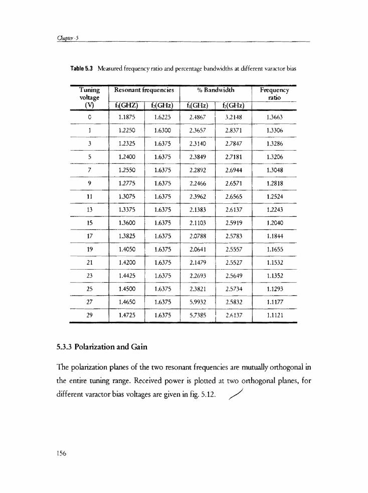
@2251.-5 2 - - _ _Table 5.3 Measured frequency ratio and percentage bandwidths at different varactor bias
i_ . - 1 —~ - **' * T“Tuning Resonantfrequencies % Bandwidth 1 ‘Frequencyvoltage 1 I300
H (v) g 1] fg1(GHZ)M5 f5(c;H2) f.(oH2)g 1 f;(GHz) .80 1.1875 1.62255 1 5 7 ; it 1 5 ‘ it 72.4867 3.2148
1%
1.3663
1 1.2250
1 .
1
1.53001
2.3657 2.83711
1.3305
311
1.2325 1.6375-1
2.3140
_1
5' 1
2.7847 1 .3286
5
71
.
1.2400 1.5375 g 2.38491.2550 1.6375
1
2.2892r.
2.7181
2.6944
1.3 206
1.3048
59
11
1.2775
1 .3075
1.6375
1.5375
2.2466
2.3962
1
5-1
2.6571
2.6565
1
1
1
1.2818
1.2524
13 1.3375 1.6375 2.1383 2.61357 1 .2243
15 1.3 600 1.6375 2.1103 2.5919 j_ 1 .2040
17I
1
1
1.3825i
1
1.6375 2.0788 2.5783 1.1844
19 1.4050 Ti . 1.6375 2.0641 2.5557 1.1555
21 1 .4200 1.63 75 2.14791
72.5527
J.-
1.1532
23 1 .4425 1.5375 2.2693 2.5649 1.1352
25 1 .4500 1.5375 2.3821 2.5734, .1
1
.L
1.1293
27 1.4650 1.6375 5.9932' 71
1
1 2.5232 1.1122
291..
1.4725 1.6375 1 5.73851
1
-42.6137
I1
1.1121
5.3.3 Polaiization and Gain
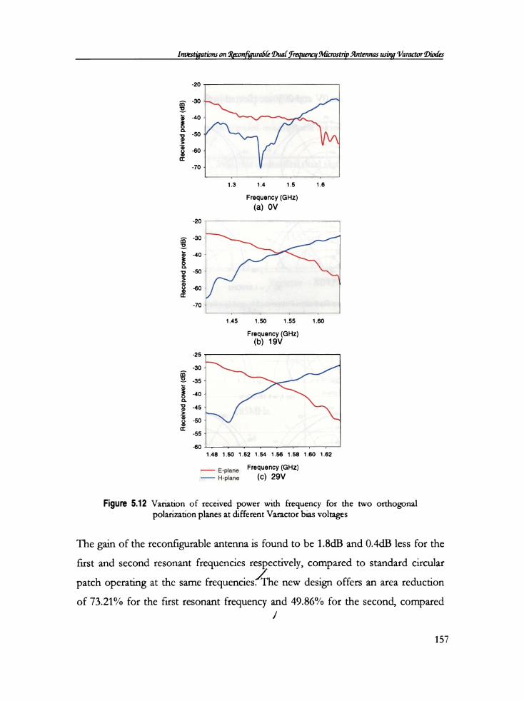
The polarization planes of the two resonant frequencies are mutually orthogonal in
the entire tuning range. Received power is plotted at two orthogonal planes, for
different varactor bias voltages are given in fig. 5.12.
156
,/
Irwe_¢t'yanbrr.s0n9(_ecorrfigwa6& Dua[fFreq‘rrena{M12:rart1'ipJ'4ntenrra.s us|'rg’Varact0r1)r'oJas
-20 —A -30-40 q
50
Rece ved power dB
60 —
.79 1 1 | r1.3 1.4 1.5 1.6Frequency (GHz)
(a) 0V.29 . 5* _ T‘. aI
IA -39 1 1
er dB
-40 .
‘ved pow
Q
4
Hece
6»O
-701.45 1.50 1.55 1.60
Frequency (GHz)(b) 19V
-25
5 -30‘-» -35*,‘
F-'lece'ved powe dB
-40
45 ~
50 1
-55
-60'-‘ i I 1 | 0 r | 01.46 1.501.52 1.54 1.56 1.58 1.60 1.62
___ E_p|ane Frequency (GHz)-—- H-plane (C) 29V
Figure 5.12 Variation of received power with frequency for the two orthogonalpolarization planes at different Varactor bias voltages
The gain of the reconfigurable antenna is found to be 1.8dB and O.4dB less for the
first and second resonant frequencies respectively, compared to standard circular
patch operating at the same frequencies.4‘ he new design offers an area reduction
of 73.21% for the first resonant frequency and 49.86% for the second, compared/
157
Cbqom -5
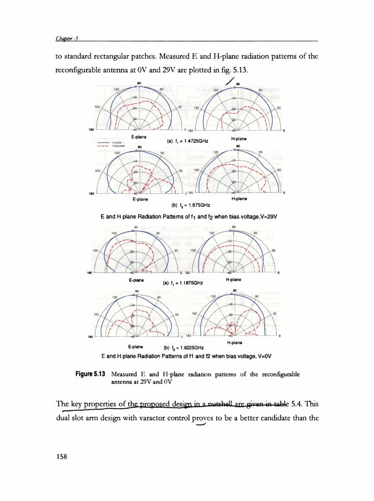
to standard rectangular patches. Measured E and H-plane radiation patterns of the
reconfigurable antenna at OV and 29V are plotted in fig. 5.13.»<> ./90120 60 1 20 60///'I. 2/ ___/=14*l—-~‘-__‘ \\__ // ___;1o1~-___ \/ J Q xi‘ " l H x1' " “ , 4"_ \. / .i*<i'”' ’ \>~i; \150 ’ A1’ ;e—A- \\3O 150 / ¢’~,-Q \ soX / ‘-1:-£'__ \ /’ p \ :29 ~ " ‘\
\ ‘I/ Ii' " ./ Y, . , a V‘. »_,_ / /A ‘7‘\ ~+~\| i
/‘iii. -D i
\ 4\\_ .\_. _ =.\
\ , -x\,3;
_;?/l’
-——-____\\_
‘ ' 'v//P‘\_\
-_ /ll_____\7{
,. ...//_lv/I _.-__ , _
111 » \‘x V11‘.\ " A . ."J)!‘ c __‘ ‘i\_
\\ ii‘Q // i
_- 4‘ 4;‘ "\._
180.? _ g la!Mane (a) 1, = 1.4725GHz *"°'a"°go 90— — — Cross-putal
en 0180 ~ -‘ he 46% l —‘— ll 4 o
120 _““"~» so f \\1 20 \~-__ 60/' i// H ;____»49 --___-______ \\ i --49 "' — —-_\_ I \_ _ . \i \i // i , ‘-\' \..7 _ \\ \ " \ __ }'\_150 _ \ 30 150 _ _ ~ 30
_ ,// /< ~ \ , it _,___. "~;.»,'z,/ , , "\~ "‘ i
‘_‘R‘_\\‘A_
_ \_g_.<\‘/ff,
‘K’ o¢:~5\4)~+\~\ x ,~ /\\_ \ _v/L/
'\I \/)<
_."'4Z‘.
*1\ '}~<-“T -/
\_$'\\\\fixe
1‘, ‘VII
x 1i I V\ __, ‘_ ’
_A-/J,
18° ‘L i _Ll:: I. il l H’ 1 O 180 L. __i_\ ii ‘ii lL_ ll. l 0E-plane H-P|a"°(b) 12 = 1.675GHz
E and H plane Radiation Pattems of f1 and f2 when bias voltage,V=29V90 90120 \f° i2° // __\'\_5°\ "‘_'\‘__ i g l ‘ 7 _ _ ‘,/ / \ \ ."/ /"L; ’ “' -_ T _ \ ;‘k“~»_ '~\1 59 i \ xi’ \ 30 1 50 / I’ 2Q~ \ 30\ | _/ it \ / La‘ ii/, ¥\\\ /'__ -r ///A; /I, 7é . a. X /’ \I /\ ‘ x \ i
l ‘\ " l /I 47 I _‘_7""—~-._ \\ ‘- ll.I Vi’ \ _ ‘ K '| , iv \§ _ )(' '1 '- |I 1 /I ‘ l‘ l 1' i _v"l,-/ ii‘ l i18° l l i VJ’ Q 18° % I in l 1 4'. 0E""°"° (a) r, = 1.1875GHz H"'a"°90 90120 ‘\ so 120, _"\\§<>,/ -, // ‘ ii _\/,'1 49+ ____x_\ I \_ / /' ' -—-\_\___/ ._ . '_ \ / * ‘ J;__ \ 30 15° / 24> #~,4' ' _ V \ IV _’ J, H .
I I,‘ _'\ i '1‘ \ ll‘ / ? ‘ ‘ll / l i
JO,\
/
//\J Igs . \ ___v‘ If
<_,,___
1- "~
X,\\_
~_‘\<
‘ti
._./'
/\.___
\\- -'
\irks‘
/'‘\
kg/,..1’ mO
.I Q
fig_ _
X \ V. 1, I ‘IQ i |' |' > :41 ll i‘Bo k _ W__k‘ 1' . I 1‘ V‘ 3 W 1 0 180 l at L. _( _?$ 1 _l OH-plane
E'P|a"° (b) f2 = 1.6225GHzE and H plane Radiation Patterns oi i1 and i2 when bias voltage, V=0V
Figure 5.13 Measured E and H-plane radiation patterns of the reconfigurableantenna at 29V and OV
The key properties of th o o ed desi ' ' ' 5.4. Thisdual slot arm design with varactor control proves to be a better candidate than the-_)
158
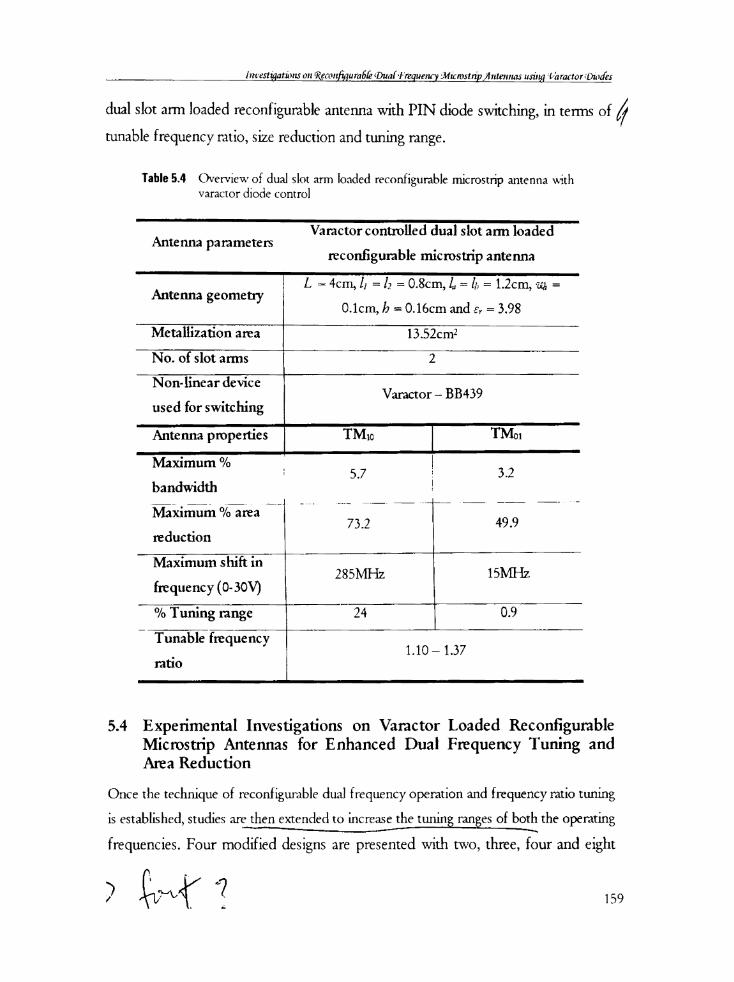
r 7- __ o __ 1"¢'@$fi§I¢11'-Ii)"-Y 011 R6601!/_igy,ra_(i!§:'<Duat'-1'fgqu_e;:§y 5M:'crostn'p/“fntemms u.tin,q "I/hractor \’D1iu_1E's
dual slot arm loaded reconfigurable antenna with PIN diode switching, in tenns of
tunable frequency ratio, size reduction and tuning range.
Table 5.4 Overview of dual slot arm loaded reconfigurable microstrip antenna withvaractor diode control“‘ —‘"‘ * 1 _o — _
Varactor controlled dual slot ann loaded iAntenna parameters
reconfigurable microstxip antenna
1 L = 4cm, 11 =12 = O.8cm, L, = [1, = 1.2cm, -w, =
Antenna geomcny 5 01 b 016 <1 3 98» CH1, = ¢ ZIII 83' = 0
Metallizatioiniiaireaiiiiii A A 13.52¢m1No’. of slotiainns E will 2 M in_ a L _ t M
Varactor — BB439Non- linear device it
used for switching
Antenna propertieS;V_
TM1o TM¢1
0/0 Ibandwidth
_Maiti1Rn1 0/aaa
reduction
15.773.2
3.2
l
l
49 .9
Maximum shift in
frequency (0-30V)
‘l _285MHz 15l\/[Hz
% Tuning rangel
24o T i 0.9
Tunable frequenc
ratio
Y
_J
10-137
5.4 Experimental Investigations on Varactor Loaded ReconfigurableMicrostfip Antennas for Enhanced Dual Frequency Tuning andArea Reduction
Once the technique of reconfigurable dual frequency operation and frequency ratio tuning
is established, studies arebthen extended to increase the tuning ranges of both the operating
frequencies. Four modified designs are presented with two, three, four and eightD ii? 159\
Chapter -5
slot arms, respectively, in order to enhance the dual frequency tuning and area
reduction.
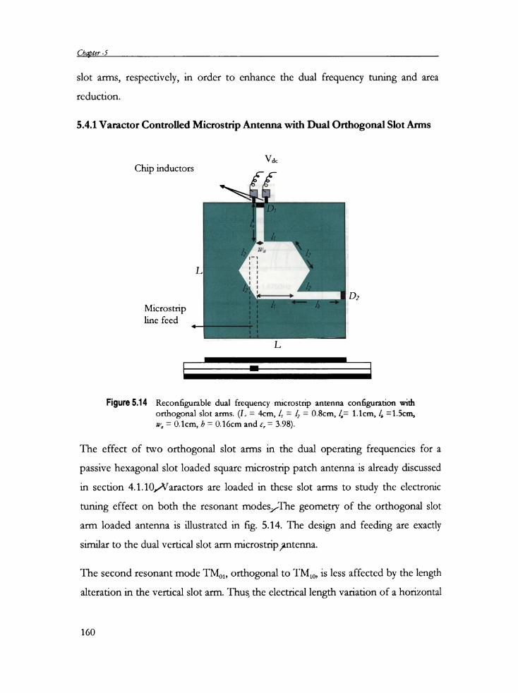
5.4.1 Varactor Controlled Microstrip Antemm with Dual Orthogonal Slot Arms
t {EChip inductors
L
D2
Microstripline feed T l
Figure 5.14 Reconfigurable dual frequency microstrip antenna configuration withorthogonal slot arms. (I . = 4cm, /, = /2 I O.8cm, /,= 1.1cm, I, =1.5cm,22/, I O.lcm, b I O.16cm and 5, = 3.98).
The effect of two orthogonal slot arms in the dual operating frequencies for a
passive hexagonal slot loaded square rnicrostrip patch antenna is already discussed
in section 4.1.10,/Varactors are loaded in these slot arms to study the electronic
tuning effect on both the resonant modes/The geometry of the orthogonal slot
arm loaded antenna is illustrated in fig. 5.14. The design and feeding are exactly
similar to the dual vertical slot arm I'l'1iC1'OSlZ1‘ip)I'lt€f1I121.
The second resonant mode TMO1, orthogonal to TM10, is less affected by the length
alteration in the vertical slot arm. Thus the electrical length variation of a horizontal
160
Imnuigmbmonflpcorlflwafik u.n'rg’I/aracwrfimfes
slot arm of length /,, and width we introduced in the patch can effectively tune the
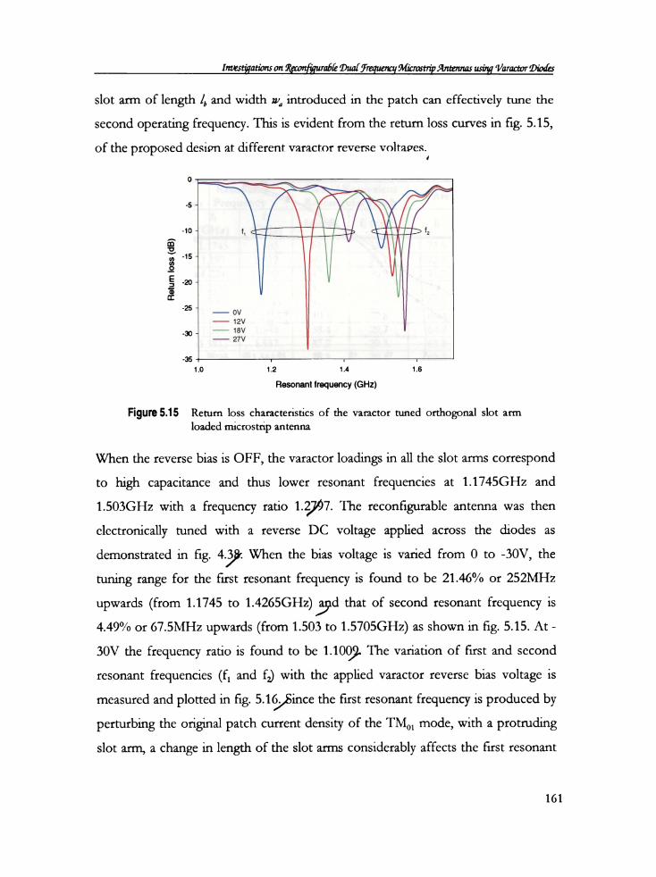
second operating frequency. This is evident from the return loss curves in fig. 5.15,
of the proposed desion at different varactor reverse voltages.(0 _-s
-10 ~ 1, git
m oss dB
++
44.._-i‘ Q
i\-4
| | ._
8.
.r
._
t _<
F ‘
Reu
\
'25 ‘ -— ov1 — 12v i301 4 18V-— 27v-35 "i 1 e n t1.0 1.2 1.4 16Resonant frequency (GHZ)
Figure 5.15 Return loss characteristics of the varactor tuned orthogonal slot armloaded rnicrostrip antenna
When the reverse bias is OFF, the varactor loadings in all the slot arms correspond
to high capacitance and thus lower resonant frequencies at 1.1745GHz and
1.503GHz with a frequency ratio 1.2]97. The reconfigurable antenna was then
electronically tuned with a reverse DC voltage applied across the diodes as
demonstrated in fig. 4.59. \X/hen the bias voltage is varied from O to -30V, thetuning range for the first resonant frequency is found to be 21.46% or 252MHz
upwards (from 1.1745 to 1.4265GHz) 9d that of second resonant frequency is4.49% or 67.5MHz upwards (from 1.503 to 1.5705GHz) as shown in fig. 5.15. At
30V the frequency ratio is found to be 1.10% The variation of first and second
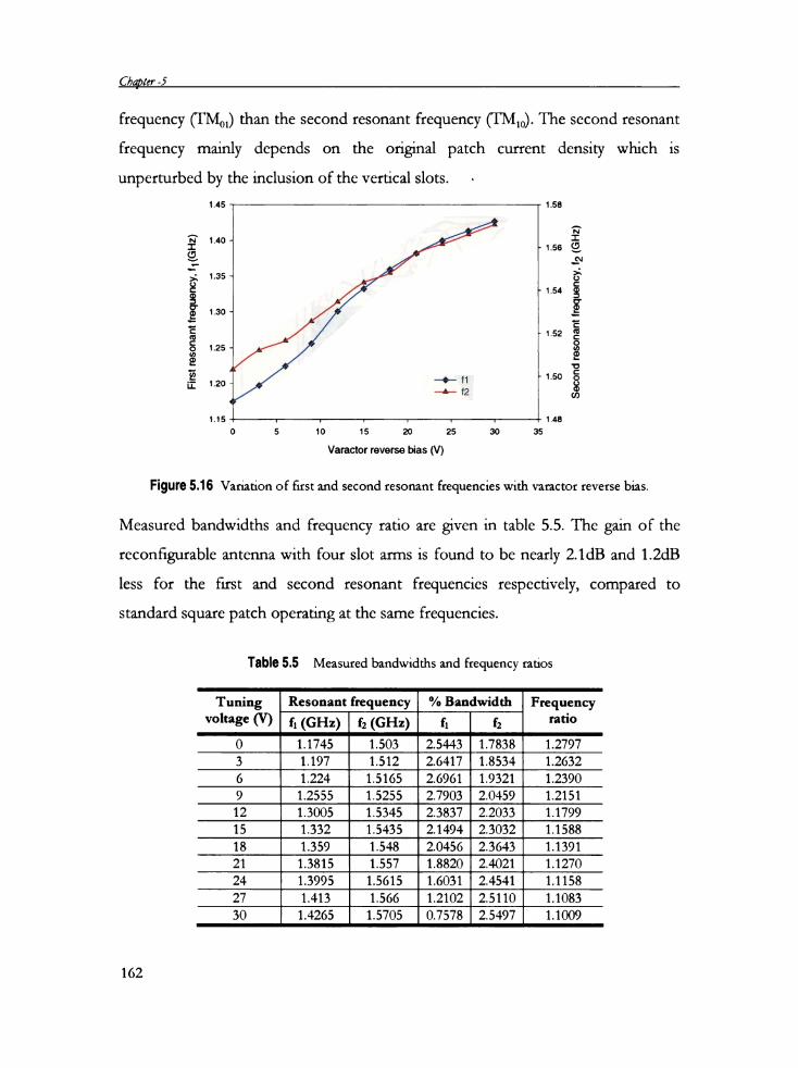
resonant frequencies (fl and fl) with the applied varactor reverse bias voltage is
measured and plotted in fig. 5.16/Since the first resonant frequency is produced by
perturbing the original patch current density of the TM01 mode, with a protruding
slot arm, a change in length of the slot arms considerably affects the first resonant
161
Chapter -5
frequency (T M01) than the second resonant frequency (TMIO). The second resonant
frequency mainly depends on the original patch current density which 1S
unperturbed by the inclusion of the vertical slots.
'13?I£5.jj
l'6qU6l'\CY,
jj
F'rs resonan
j
Figure 5.15 Variation of first and second resonant frequencies with varactor reverse bias
Measured bandwidths and frequency ratio are given in table 5.5. The gain of the
reconfigurable antenna with four slot arms is found to be nearly 2.1dB and 1 2dB
less for the first and second resonant frequencies respectively, compared to
1.45
1.40
-A
(Q)(,1I
1.30
1.25
1.20 -1
1.15 -1 1 1 1 1 1 1
_
0 5 10 15 20 25 30 35Varactor reverse bias (V)
standard square patch operating at the same frequencies.
Tuning Resonant frequency % Bandwidth Frequency
F
1.58
Hz
1.5
O3
%j
52b
requency, 2 G
jj
,1; :
52 52O NSecond resonan
1.48
Table 5.5 Measured bandwidths and frequency ratios
v<>l¢=g<= (V) r, (G111) £2 (cm) r, r, M0
Q
1.1745 1.503 2.5443 1.7838 1.2797
U3
1.197 1.512 2.6417 1.8534 1.2632
C\
1.224 1.5165 2.6961 1.9321 1.23909 1.2555 1.5255 2.7903 2.0459 1.215112 1.3005 1.5345 2.3837 2.2033 1.179915 1.332 1.5435 2.1494 2.3032 1.158818 1.359 1.548 2.0456 2.3643 1.139121 1.3815 1.557 1.8820 2.4021 1.127024 1.3995 1.5615 1.6031 2.4541 1.115827 1.413 1.566 1.2102 2.5110 1.1083
162
1.4265 1.5705 0.7578 2.5497 1.1009
I nve.st'yat1'0r|s on Rgronflgurafié 1)ua[jFreq‘uena{ £Micrast1ip J'4nt2rma.s usirg ‘Varacwr Diodes
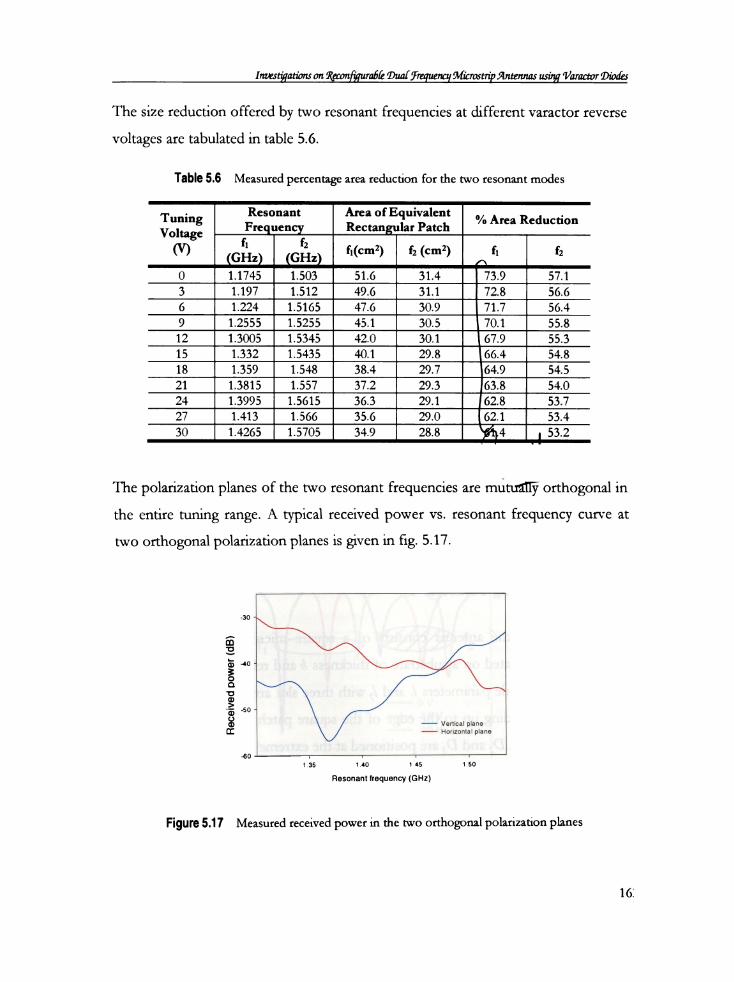
The size reduction offered by two resonant frequencies at different varactor reverse
voltages are tabulated in table 5.6.
Table 5.5 Measured percentage area reduction for the two resonant modes
Voltage requency ectangu ar atcr(V) ‘ '2 f1(cm2) £2 (¢m=)
O
Tuning Pllesonant 1;:-ea of E(l|ui\lr)alen; % Area Reduction
GHz1.1745
GHz1.503 51.6 31.4
f1 f273.9 57.1
DJ
1.197 1.512 49.6 31.1 72.8 56.6
G\
1.224 1.5165 47.6 30.9 71.7 56.49 1.2555 1.5255 45.1 30.5 70. 1 55.812 1.3005 1.5345 42.0 30.1 67.9 55.315 1.332 1.5435 40.1 29.8 66.4 54.818 1.359 1.548 38.4 29.7 64.9 54.521 1.3815 1.557 37.2 29.3 63.8 54.024 1.3995 1.5615 36.3 29.1 62.8 53.727 1.413 1.566 35.6 29.0 62.1 53.43O
The polarization planes of the two resonant frequencies are mutua‘[l'}7 orthogonal in
the entire tuning range. A typical received power vs. resonant frequency curve at
1.4265 1.5705 34.9 28.8
two orthogonal polarization planes is given in fig. 5.17.
Figure 5.17 Measured received power in the two orthogonal polarization planes
4
30
i
dB
&
QwerLo
Rece ved 06»o
1
i Vemcal plane—— Honzontal plane
-60 11.35 1.40 1 45 1 SOResonant frequency (GHz)
53.2
Cbqvter -5
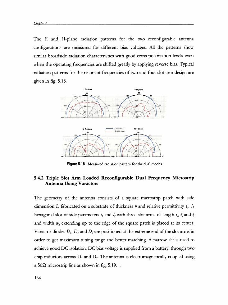
The E and H-plane radiation patterns for the two reconfigurable antenna
configurations are measured for different bias voltages. All the pattems show
similar broadside radiation characteristics with good cross polarization levels even
when the operating frequencies are shifted greatly by applying reverse bias. Typical
radiation patterns for the resonant frequencies of two and four slot arm design are
given in fig. 5.18.
H E-plane 11 H-planego 90-_ ac ‘Q0 , if q ‘:49 .. _,____> ‘ ‘ I p_ _ _.4O—- — ~--_ AZ. / ‘ * y ‘ T’ X‘ Y ’5» / T . 30 ~50 _ , _ Ha» 30
Ci / T __ Q i i i “ .4—"‘): X /V ji/I x_7"'». » ___ L \ i -‘Iii ii.
-. ii 1 ii l 1‘: T ii l 15g i l ‘iv l /\ ii180 -40 O ~f2 E-plgng T“ CO'POl3l l2H-plflflfl9° — — — Cross-po=ar 0°120 6" 120/‘ \ 60
. ‘ J ____r9_ - ______V> . » /‘ i“ ‘ 7___;i3_ . r- i ". \.. "I T /1 \st T , -:£_A \.._ so 150 / ,' _.¢ 1;. I” T 30\ i‘ -‘ [ i. I , 1‘ . . y I , - . _ \4 1. 0\ . 1 ‘_ i‘ \ . i‘ "'=,'l \ y i ‘. l. i‘ ~. ‘ i ,»' l ; = ‘ ‘ y 7- l\ ' l ~ ._ _ ~ i ‘ l \180i I I I l Lo-1804' i__ i __‘._.Figure 5.13 Measured radiation pattern for the dual modes
5.4.2 Triple Slot Arm Loaded Reconfigurable Dual Frequency MicrostripAntenna Using Varactors
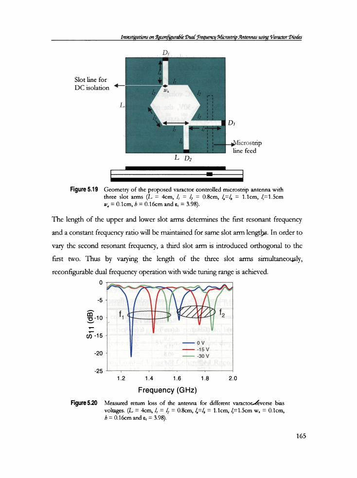
The geometry of the antenna consists of a square microstrip patch with side
dimension L fabricated on a substrate of thickness /9 and relative permittivity er. A
hexagonal slot of side parameters /, and /2 with three slot arms of length /4, /,, and /t
and width we extending up to the edge of the square patch is placed at its center.
Varactor diodes D,, D2 and D, are positioned at the extreme end of the slot arms in
order to get maximum tuning range and better matching. A narrow slit is used to
achieve good DC isolation. DC bias voltage is supplied from a battery, through two
chip inductors across D1 and D2. The antenna is electromagnetically coupled using
a 5052 microstrip line as shown in fig. 5.19. ,
164
Irwemgations on Keconfywafié Dualfrequency iMicr0st11'p fllntermas usirg ‘Varactvr Q)io&.s
Q1
Slot line forDC isolation 4_
L
D3
._,Microstripline feed
LD2
Figure 5.19 Geometry of the proposed varactor controlled microstrip antenna withthree slot arms (L I 4cm, /, I /2 I O.8cm, /,I/,, I 1.1cm, /,I1.5cm22/, I O.1cm, /2 I O.16cm and e, I 3.98).
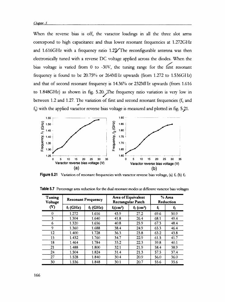
The length of the upper and lower slot arms determines the first resonant frequency
and a constant frequency ratio will be maintained for same slot arm lengths. In order to
vary the second resonant frequency, a third slot arm is introduced orthogonal to the
first two. Thus by varying the length of the three slot arms simultaneously,
reconfigurable dual frequency operation with wide tuning range is achieved.O
-5
<qB>E3
$11a
iov-—-15v'20 ' —— -so v-25 1 1 I 1 11.2 1.4 1.6 1.8 2.0
Frequency (GHz)
Figure 5.20 Measured return loss of the antenna for different varactorneverse biasvoltages. (L I 4cm, Z, I /2 I O.8cm, l,Il,, I 1.1cm, LI1.5cm W, I O.1cm,/1 I O.16cm and e, I 3.98).
165
Cbqbter -5
\X/hen the reverse bias is off, the varactor loadings in all the three slot arms
correspond to high capacitance and thus lower resonant frequencies at 1.272GHz
and 1.616GHz with a frequency ratio 1.2VThe reconfigurable antenna was then
electronically tuned with a reverse DC voltage applied across the diodes. \X/hen the
bias voltage is varied from O to -30V, the tuning range for the Flgt resonant
frequency is found to be 20.75% or 264MHz upwards (from 1.272 to 1.536GI Iz)
and that of second resonant frequency is 14.36% or 232l\'fl Iz upwards (from 1.616
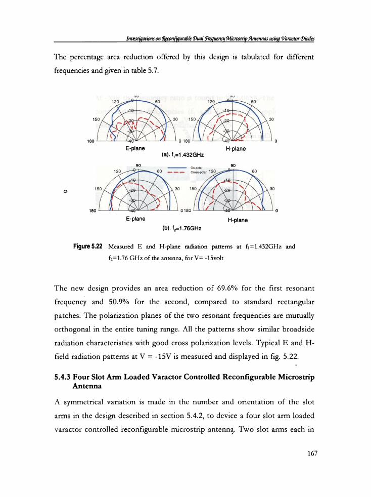
to 1.848GHz) as shown in fig. 5.20/Yhe frequency ratio variation is very low inbetween 1.2 and 1.27. The variation of first and second resonant frequencies (fl andIfl) with the applied varactor reverse bias voltage is measured and plotted in fig. 5.21.
1.55 if — 1-90 *5 we 5~- -———.50 1 '"’ 1
Hz
Hz
8
45 " 80} 1l I1.70
Frequenc
é Z1
8 ______ .
Frequen
5
8') ?__
v.1G
sf
Cyv2G
ge
1_2s <1 1 1 1 1 1 v — 1 ' ' ' ' '0 5 10 15 20 25 30 0 5 10 15 20 25 30VaTa¢l°' reverse bias V°|l399 (V) Varactor reverse bias voltage (V)(a) (0)
Figure 5.21 Variation of resonant frequencies with varactor reverse bias voltage, (a) f1 f2
Tflblé 5.7 Percentage area reduction for the dual resonant modes at different varactor bias voltages
Tunin Area of E uivalen °g Resonant Frequency q t /0 AreaVoltage _ Rectangular Patch Reduction(V) ( 2) ( 2) fl fzf1 f2 f1 cm fg Cm1.272 1.616 4 . 27.2 . .3 1.304 1.640 41.8 26.4 68.1 49.46 1.320 1.656 40.8 25.9 67.3 48.49 1.360 1.688 38.4 24.9 65.3 46.412 1.400 1.728 36.3 23.8 63.2 43.815 1.432 1.760 34.7 22.9 61.5 41.718 1.464 1.784 33.2 22.3 59.8 40.121 1.488 1.800 ‘ 32.1 21.9 58.4 38.924 1.504 1.824 31.4 21.3 57.5 37.427 1.528 1.840 30.4 20.9 56.0 36.01.536 1.848 . . . .166
Irwe.st1yatian.s on 9(p:anfigura6lZz 1)ua[9'requena{ ‘I/aradvr Diodes
The percentage area reduction offered by this design is tabulated for different
frequencies and given in table 5.7.
/1%? .lYu§2.%i.®P\\\o 180 ~=lane H-plane
(3)- f1='l .432GHZ
bit."I 557'Y!9
90 90_ i Co-polar _C) 150
?Q.%
S‘gt.:2i
0180P|3"9 H-plane(b). f2=1.76GHz
Figure 5.22 Measured E and H-plane radiation patterns at f1=1.432GHz and
f2=1.76 GHz of the antenna, for V= -15volt
The new design provides an area reduction of 69.6% for the first resonant
frequency and 50.9% for the second, compared to standard rectangular
patches. The polarization planes of the two resonant frequencies are mutually
orthogonal in the entire tuning range. All the patterns show similar broadside
radiation characteristics with good cross polarization levels. Typical E and H
field radiation patterns at V = -15V is measured and displayed in fig. 5.22. .
5.4.3 Four Slot Arm Loaded Varactor Controlled Reconfigurable MicrostripAntenna
A symmetrical variation is made in the number and orientation of the slot
arms in the design described in section 5.4.2, to device a four slot arm loaded
varactor controlled reconfigurable microstrip antenna. Two slot arms each in
167
flbapter -5
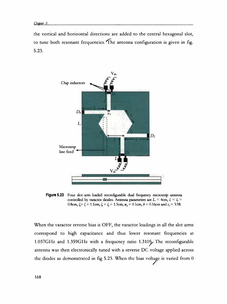
the vertical and horizontal directions are added to the central hexagonal slot,
to tune both resonant frequencies/fhe antenna configuration is given in fig.5.23.
Vdc
Chip inductors \ ({5
D4
L
D2
Microstripline feed ‘
.25L:Figure 5.23 Four slot arm loaded reconfigurable dual frequency microstrip antenna
controlled by varactor diodes. Antenna parameters are L = 4cm, I, = 1, =O.8cm, /,= /,= 1.1crn, /,, = 1,, I 1.5cm, 21/, = O.1cm, b I O.16cm and e, = 3.98.
When the varactor reverse bias is OFF, the varactor loadings in all the slot arms
correspond to high capacitance and thus lower resonant frequencies at
1.037GHz and 1.359GHz with a frequency ratio 1.310? The reconfigurableantenna was then electronically tuned with a reverse DC voltage applied across
the diodes as demonstrated in fig 5.23. \X/hen the bias voltye is varied from 0
168
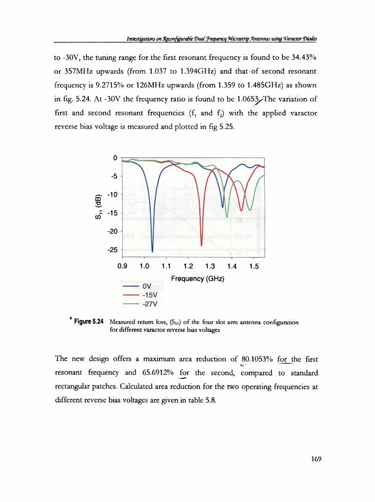
I rwest§gation.s on Kecanfiywafik Dzmljfrequerrcy Mfi:ra:¢1'§v fllntennas usirg ‘Varactvr Qliorfes
to -30V, the tuning range for the first resonant frequency is found to be 34.43%
or 357MHz upwards (from 1.037 to 1.394GHz) and that of second resonant
frequency is 9.2715°/0 or 126MHz upwards (from 1.359 to l.485GHz) as shown
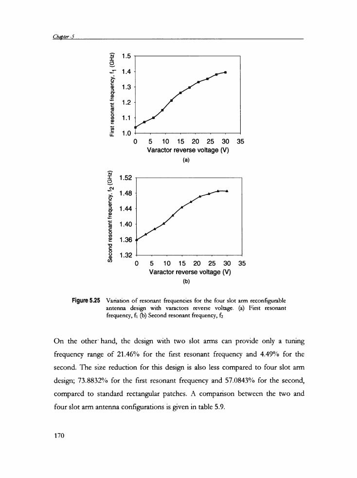
in fig. 5.24. At -30V the frequency ratio is found to be 1.0653/The variation of
first and second resonant frequencies (fl and f2) with the applied varactor
reverse bias voltage is measured and plotted in fig 5.25.
Q to .. 5
gii Y‘E l/B .mi -15 *
-29 _
-25 *I 1 1 1 1 n t0.9 1.0 1.1 1.2 1.3 1.4 1.5
Frequency (GHz)i OV-— -15v—-- -27v
1 Figure 5.24 Measured return loss, (S11) of the four slot arm antenna configurationfor different varactor reverse bias voltages
The new design offers a maximum area reduction of 80.1053°/o for the first
resonant frequency and 65.6912°/0 for the second, compared to standard
rectangular patches. Calculated area reduction for the two operating frequencies at
different reverse bias voltages are given in table 5.8.
169
C/)q>ter -5
A 1.5
1 GHZ
1.4
cy,
1.3
frequen
.. 1.2
nan
1.1
GSO
i1
F'rs r
1.0 = - - - - ~ - O 5 10 15 20 25 30 35
Varactor reverse voltage (V)(8)i
1.52
"_ 1.48
uency, 2 GHz
1.44
req
3 1.40
cond resonan
1.36
1.32 ~ ~ » - - - i 0 5 10 15 20 25 30 35
Varactor reverse voltage (V)(b)
Se
Figure 5.25 Variation of resonant frequencies for the four slot arm reconfigurableantenna design with varactors reverse voltage. (a) First resonantfrequency, fl Second resonant frequency, f2
On the other‘ hand, the design with two slot arms can provide only a tuning
frequency range of 21.46% for the first resonant frequency and 4.49% for the
second. The size reduction for this design is also less compared to four slot arm
design; 73.8832% for the first resonant frequency and 57.0843”/0 for the second,
compared to standard rectangular patches. A comparison between the two and
four slot arm antenna configurations is given in table 5.9.
170
_ _ g !1;t.~est;'qq£_1p_r_1s_1J_niigconfigurafifiz 1Du51_f_*17g(eg11e1u7_y ;’l117rrostr17p/I -rrtennas u_.117r1_q ('1/Qgractor fD17oz{es
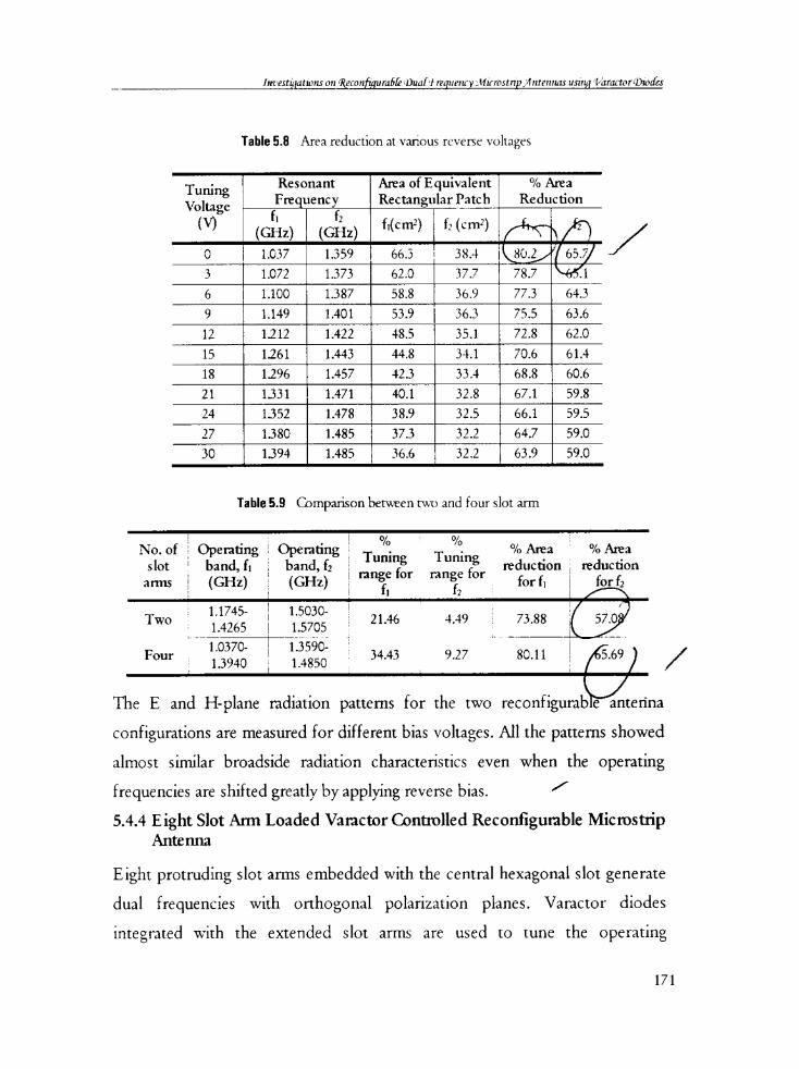
Table 5.3 Area reduction at vmous reverse voltages
1.1.7.... 71 Resonant Area of Equivalent % AreaFrequency Rectangular Patch Reduction.. 1 . . 1-- [Voltage
(V) f f , _(C1112) i (61312) f1(cm-) fg cm?1
1
1 1.037__4 l1-973..-._2
LHIO
f ( ) i 2 /7 1.359 667.377; 38.4 ML 1_=8g0.J2/7 65.7 1.373 7 377 ‘ 8.1 62.0 I 7 7 H-.1_
1 1.100
O'\
2-... 1 1.387 587.787 3 36.9 77.3 H 64.3A 1.149
\D
7 7 77 17.740177. 53.97"“? 36.3 UA 75.5 A 63.612 § 1212 “£4272” 7
. ,148.5 ‘ 72.8 62.0771726115 1 1 1.443 777744.787 77734.1 1 70.6 61.4
18 “M1296 . 1.457 42.3 “ 33.4 77 777 68.8 760.764
21 1331U Q 1.471 40.717777448 . 47-1-3 52-324 1.352 g27 ; 1380
1.478 7 738.91.485
an 32.5 466.1 59.564.7 59.037.3 __32.2W 1
7370 7 M1394 1.485 1 36.6 1 32.21 1' 1 .__.f?_9_'9__
Table 5.9 Comparison between two and four slot arm
1 1___.. 7 "—"”XF . 4-I--a -JI II _ _ 1 o _ 0 .No. of Operating Operatmg 5 /O. /0. °/6 Area % Areaslot f band, f1am1s (GHZ)
1 1.5030Two
1 0370- 1 3590Four
A
-—1
Tumng Tuningband, f; inn efor ran efor reduction; reduction(GHz) fil fig 1616 1 for 1,1 1745- . ..
g H265 A 15705 21.46 4.49 73.88. .- . 115940 M850 ._ 34.43 L 9.27 80.11 E 5.69 /____.. _ 7 .1 77 7 77 77 77777777
The E and H-plane radiation patterns for the two reconfigurabe antenna
configurations are measured for different bias voltages. All the patterns showed
almost similar broadside radiation characteristics even when the operating
frequencies are shifted greatly by applying reverse bias. -/
5.4.4 Eight Slot Arm Loaded Varactor Controlled Reconfigurable MicrostripAntenna
Eight protruding slot arms embedded with the central hexagonal slot generate
dual frequencies with orthogonal polarization planes. Varactor diodes
integrated with the extended slot arms are used to tune the operating
171
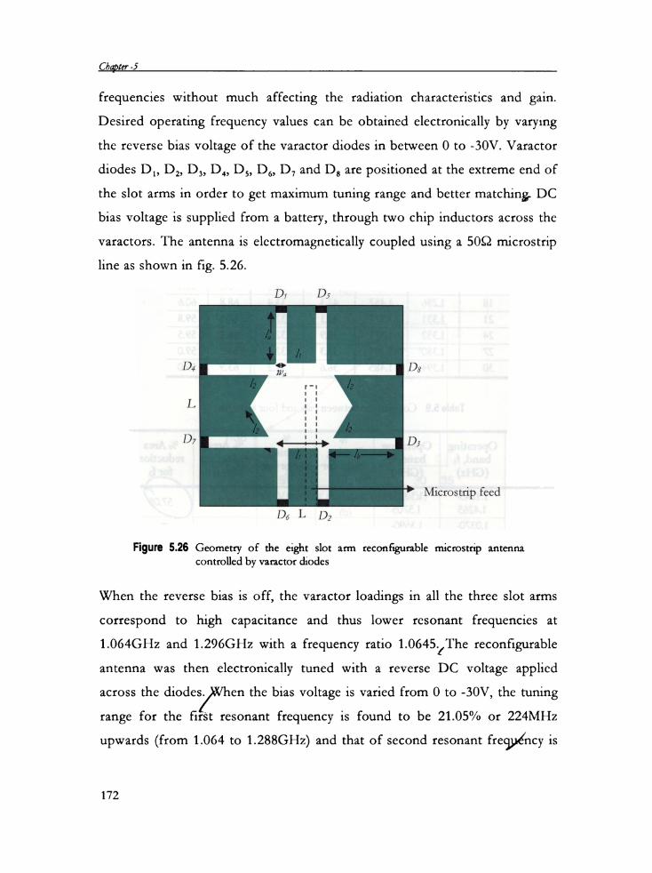
C/2z¢ter -5
frequencies without much affecting the radiation characteristics and gain.
Desired operating frequency values can be obtained electronically by varying
the reverse bias voltage of the varactor diodes in between O to -30V. Varactor
diodes D1, D2, D3, D4, D5, D6, D7 and D8 are positioned at the extreme end of
the slot arms in order to get maximum tuning range and better matching. DC
bias voltage is supplied from a battery, through two chip inductors across the
varactors. The antenna is electromagnetically coupled using a SOQ microstrip
line as shown in fig. 5.26.
D1 D,
D4 1 D3LD7 D3
'7 Microstrip feed
1), L 1),
Figure 5.26 Geometry of the eight slot arm reconfigurable microstrip antennacontrolled by varactor diodes
When the reverse bias is off, the varactor loadings in all the three slot arms
correspond to high capacitance and thus lower resonant frequencies at
1.064GHz and 1.296GHz with a frequency ratio 1.0645.(The reconfigurableantenna was then electronically tuned with a reverse DC voltage applied
across the diodes/When the bias voltage is varied from 0 to -30V, the tuningrange for the first resonant frequency is found to be 21.05% or 224MHz
upwards (from 1.064 to 1.288GHz) and that of second resonant frequency is
172
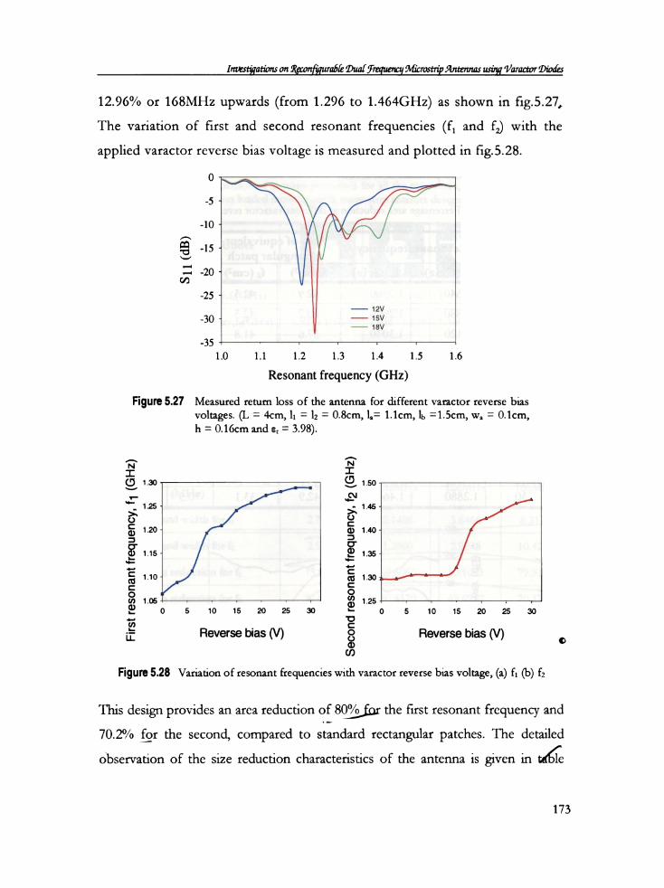
Immtggaflbns on Rp:0nflg'ura6& Dzmffrequmcy flbfxtramipfirztennas usirg ‘I/araavrflodks
12.96% or 168MHz upwards (from 1.296 to 1.464GHz) as shown in f1g.5.27,
The variation of first and second resonant frequencies (fl and fl) with the
applied varactor reverse bias voltage is measured and plotted in f1g.5.28.
$11 (dB)
-\ \_ \-5 - \\\ .'10 ' V /ii /‘*\\ ‘If-15 la
-20
-25 — 12v_3() - -- 15V
1 — 18V-35 '1' » 1 1 r I 11.0 1.1 1.2 1.3 1.4 1.5 1.6Resonant frequency (GHz)
Figure 5.27 Measured return loss of the antenna for different varactor reverse bias
(GHz)F rst resonant frequency, f1
Q
1 .25
-5N)@
_aLaU1
—l
QO5
voltages. (L = 4cm, 11 = lg = O.8cm, l,= 1.1cm, lb =1.5cm, W, = O.1cm,h = O.16cm and e, = 3.98).
(GHz)onant frequency, f2
Q £2 E E
1 n1
4
i0 5 10 15 20 25 30V V Y Y I
Second res
5».
O 5 10 15 20 25 30Reverse bias (V) Reverse bias (V)
Figure 5.23 Variation of resonant frequencies with varactor reverse bias voltage, (a) fl f2
This design provides an area reduction of 8W the first resonant frequency and
70.2% for the second, compared to standard rectangular patches. The detailed
observation of the size reduction characteristics of the antenna is given in ttge
173
0
C/mpter -5
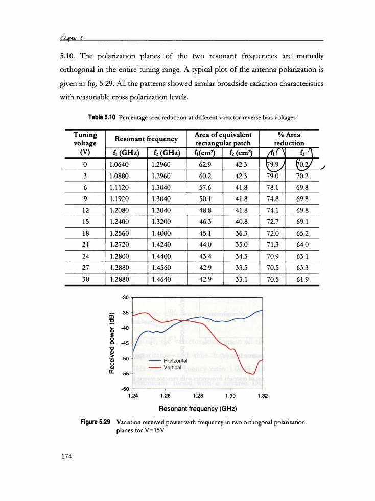
5.10. The polarization planes of the two resonant frequencies are mutually
orthogonal in the entire tuning range. A typical plot of the antenna polarization is
given in fig. 5.29. All the patterns showed similar broadside radiation characteristics
with reasonable cross polarization levels.
Tflblfl 5.10 Percentage area reduction at different varactor reverse bias voltages
Tuning Rcsonam fie uenc Area of equivalent °/6 Areavoltage J y rectan lar atch reduction(V) r, (01-11) £2 (Gm) r,(¢m1) r, (6611)0 1.0640 1.2960 62.9 42.3 W vw /3 1.0880 1.2960 60.2 42.3 79.0 70.26 1.1120 1.3040 57.6 i 41.8 78.1 69.89 1.1920 1.3040 50.1 41.8 74.8 69.812 1.2080 1.3040 48.8 41.8 74.1 69.815 1.2400 1.3200 46.3 40.8 72.7 69.118 1.2560 1.4000 45.1 36.3 72.0 65.221 1.2720 1.4240 44.0 35.0 71.3 64.024 1.2800 1.4400 43.4 34.3 70.9 63.127 1.2880 1.4560 42.9 33.5 70.5 63.330 1.2880 1.4640 42.9 33.1 70.5 61.9-3Q -|. .
A -35
B
4
e ved power d
-40 _
45 1
'- '50 " i Horizontal-i Vertical
Rec
55~
-60 ‘i - 1 "r- 1 " 11.24 1.26 1.28 1.30 1.32Resonant frequency (GHz)
Figure 5.29 Variation received power with frequency in two orthogonal polarizationplanes for V=15V
174
Irwt'.st'gat1'0r|s on Rgcoriflgurafiliz Q)ua[freq‘uency Micrastvip fllntennas 'Varactvr Dioifas
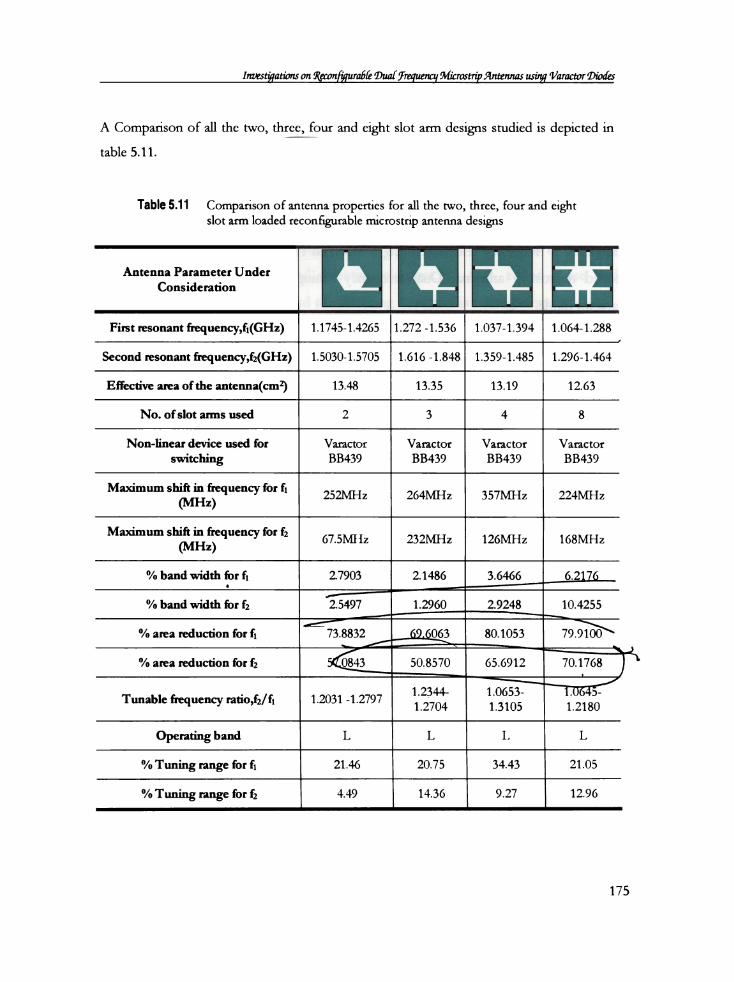
A Comparison of all the two, three, four and eight slot arm designs studied is depicted in
table 5.11.
Table 5.11 Comparison of antenna properties for all the two, three, four and eightslot arm loaded reconfigurable microstrip antenna designs
Antenna Parameter UnderConsideration
First resonant frequency,f1(GHz) 1.1745-1.4265 1.272-1.536 1.037-1.394 1.064—1.288
Second resonant frequency,f2(GI-Iz) 1.5030-1.5705 1.616-1.848 1.359-1.485 1.296-1.464
Effective area of the antenna(cm7) 13.48 13.35 13.19 12.63
No. of slot arms used 2 3 4 8
Non-linear device used forswitching
VaractorBB439
VaractorBB439
VaractorBB439
VaractorBB439
Maximum shift in frequency for f1(MI-Iz)
252MHz 264MHz 3571\/[Hz 224MHz
Maximum shift in frequency for f;(MHZ)
67.5MHz 232MHz 126I\/[Hz 168MHz
% band width for f1 27903 2.1486
% band width for fz
3.6466 6.21.2.5497 1.2960 2.9248% area reduction for fl
10.4255
% area reduction for f;
Tunable frequency ratio,f;/f1
73.8832 063 80.1053 79.9100' 0843 50 8570 65 6912 70 1768
12031 _ 12797 1.23% 1.0653- . >1.2704 1.3105 1.2180
Operating band L L L L% Tuning range for f1 21.46 20.75 34.43 21.05
% Tuning range for f2 4.49 14.36 9.27 12.96
5.5 Independent Frequency Tuning in Hexagonal Slot Loaded MicrosnipAntenna Using Modified Slot Ann
Dual frequency patch antennas may provide an altemative to large-bandwidth
antennas. The key to providing a flexible solution is to have the radiators relatively
independent. We can achieve dual frequency microstrip antenna design with
independent frequency selection, using a modified slot ann in the hexagonal slot
loaded microstiip antenna. Dual frequency tuning has been realised using avaractor diode. i5.5.1 C-Shaped Slot Loaded Reconfigurable Micmstrip Antenna
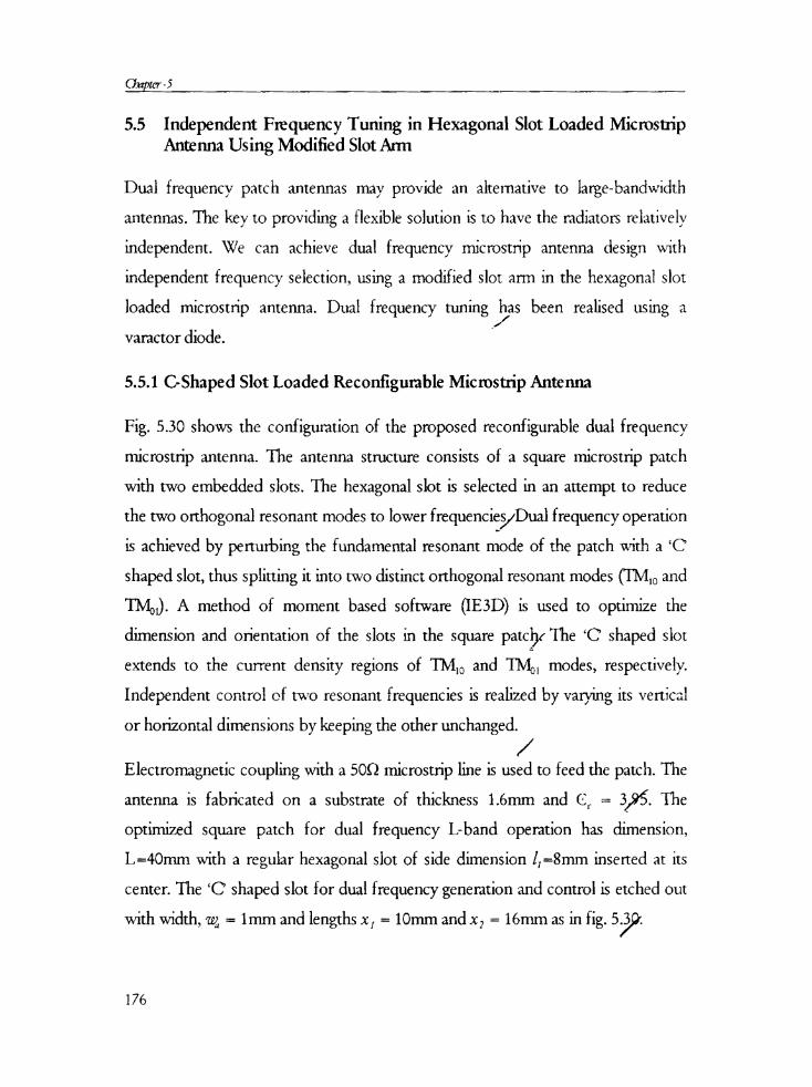
Fig. 5.30 shows the configuration of the proposed reconfigurable dual frequency
microstrip antenna. The antenna structure consists of a square microstrip patch
with two embedded slots. The hexagonal slot is selected in an attempt to reduce
the two orthogonal resonant modes to lower frequencies/Dual frequency operation
is achieved by perturbing the fundamental resonant mode of the patch with a ‘C’
shaped slot, thus splitting it into two distinct orthogonal resonant modes (TM,0 and
A method of moment based software (lE3D) is used to optimize the
dimension and orientation of the slots in the square patcly The ‘C shaped slot
extends to the current density regions of TM“, and TML, modes, respectively.
Independent control of two resonant frequencies is realized by varying its vertical
or horizontal dimensions by keeping the other unchanged./Electromagnetic coupling with a SOQ microstnp line is used to feed the patch. The
antenna is fabricated on a substrate of thickness 1.6mm and (fir = 3_/95’. The
optimized square patch for dual frequency L—band operation has dimension,
L=4Omm with a regular hexagonal slot of side dimension l,=8mm inserted at its
center. The ‘C shaped slot for dual frequency generation and control is etched out
with width, rig, = 1mm and lengths x, =10mm and x2 = 16mm as in fig. 5%
176
Irwe.st'gatiar|s on ifigconfiywafili Duaf 9'reque1u:y fllntermas usiry ‘I/aracwr Zliodies
Electronic tuning of both modes is accomplished by a varactor diode integrated
across the slot. The junction capacitance of the varactor varies against the
reverse bias applied and these different capacitive loadings correspond to
different electrical lengths and thus different resonant frequencieé/DC bias isapplied across the varactor through two chip inductors. A narrow slot line is
carved in the patch for dc isolation. Transmission lines are avoided in between
the nonlinear components and radiating element, so that, added noise and
ohmic losses are suppressed and the resulting structure is more(c0/mpact.
aractor diodeD1
Slot line forDC isolation
L
Microstrip —Hnefeed
(*1)
(b)
Figure 5.30 Schematic diagram of proposed reconfigurable microstrip antenna (a)Top view, (b) Side view. The antenna parameters are L = 40mm,/,= 8mm, /2 = 1.6mm, we = lmm, x, = 10mm, x_, = 16mm, €, I 3.95
177
Chapter -5 0 _-5_ fI
pg -10 ~ r, 12w?
-15 -.
-2° " — X2 =1Omm-— X2 = 8mmi x2 = 5mm-25 1 | e 1 | 1 11.0 1.2 1.4 1.6 1.8 2.0
Resonant frequency (GHz)(a)
0_5- i-10 ~ t/\ 1 f@ 2
BU)’ '15 "
1
'20 ' __ x, = 16mmi x,=12mmi x,=1Omm-25 ’ 1 1 1* | 1 11.0 1.2 1.4 1.6 1.8 2.0
Resonant frequency (GHz)
(b)
Figure 5.31 Variation of resonant frequencies with ‘C’ slot dimension (a) x1 = 16mmand X2 varying x2 = 10mm and x1 varying
5.5.1.1 Independent Tuning of Dual Resonant Modes
The fundamental resonant frequency of the unslotted square patch is 1.885GHz.
By etching the hexagonal slot at its center it reduces to 1.74GH;/With ‘C’ slot, two
distinct resonant modes (T M10 and TMO1) at 1.472GHz and 1.752G§z have been
178
Irwesfgatians on Kpconflurafife 1)ua[9'requern:qMz'crast1'ipfllntznnas usbg ‘Varactorflioafes
observed with a frequency ratio 1.19. Difierent ‘C’ slot dimensions, x, and x2, weretried to prove the independent frequency tuning capability of the proposed design.
It was found that the first resonant frequency, fl can be tuned without affecting f2,
by varying x, and keeping x2 unchangecgimilarly, second resonant frequency, f2
can be tuned by varying x2 and keeping x, constant. The findings are depicted in
fig. 5.31.
0 _
- it .. \/_ I1 —l‘l I2
c ent (dBco-eff‘
ES
-15
HC10
_ — ov-20 - __—— 1sv
Ref e
'25 I I I I I1.4 1.5 1.6 1.7 1.8Resonant frequency (GHz)
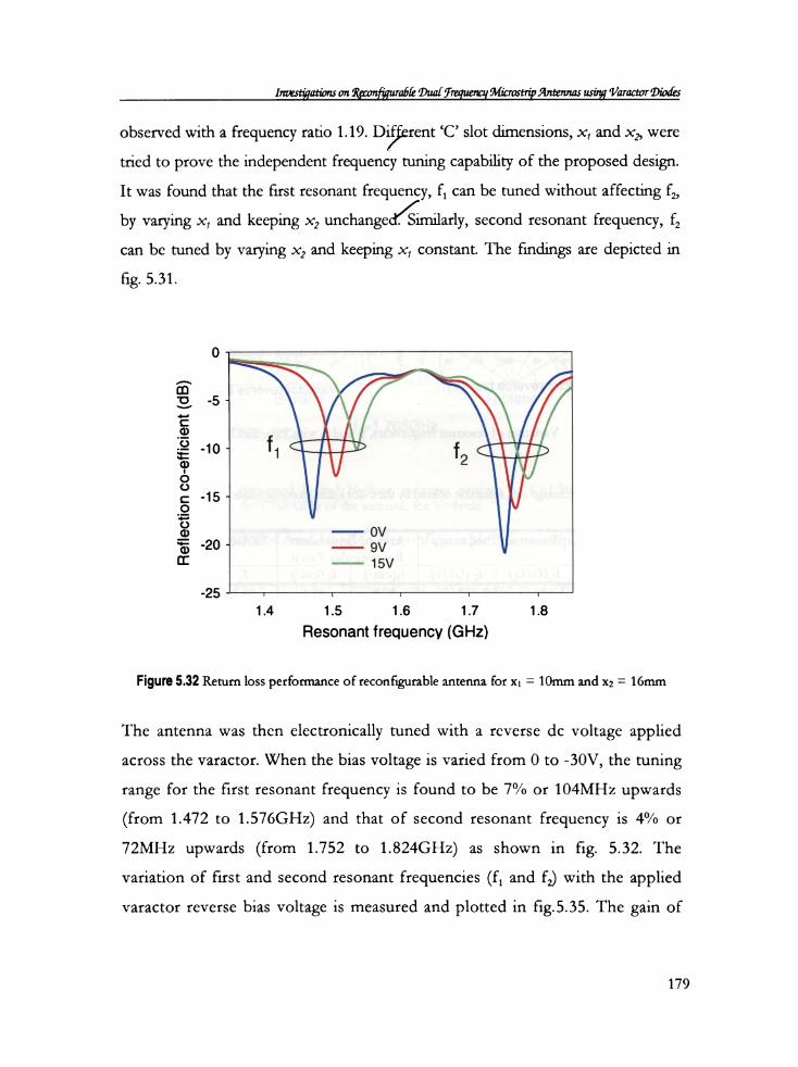
FIQUIG 5.32 Return loss performance of reconfigurable antenna for x1 = 10mm and X2 = 16mm
The antenna was then electronically tuned with a reverse dc voltage applied
across the varactor. When the bias voltage is varied from O to -30V, the tuning
range for the first resonant frequency is found to be 7% or 104MHz upwards
(from 1.472 to 1.576GHz) and that of second resonant frequency is 4% or
72MHz upwards (from 1.752 to 1.824GHz) as shown in fig. 5.32. The
variation of first and second resonant frequencies (fl and f2) with the applied
varactor reverse bias voltage is measured and plotted in f1g.5.35. The gain of
179
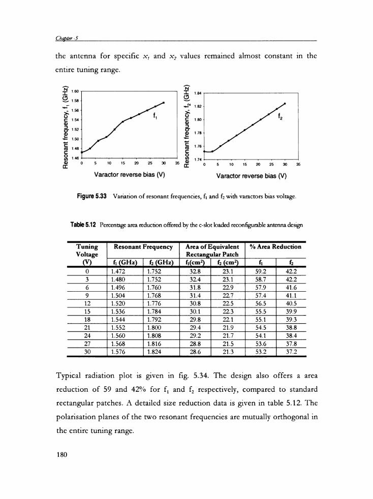
Ch4mw=5
the antenna for specific x, and X2 values remained almost constant in the
entire tuning range.
Hz)
§
y,f G§
%
onant frequenc2% é é 5E
11
Res
Varactor reverse bias (V)
IO 5 10 15 20 25 30 35
2 (GHZ)
1.84
1.82
cy, f
1.80
equen
1.78
Resonant fr
1.76
-1Q#
i i i0 5 10 15 20 25 30 35Varactor reverse bias (V)
Figure 5.33 Variation of resonant frequencies, fl and fg with varactors bias voltage.
Table 5.12 Percentage area reduction offered by the c-slot loaded reconfigurable antenna design
TuningVoltage _
Resonant Frequency Area of Equivalent % Area ReductionRectangular Patch
1.752 2.(V) f1 f2 f1! C1112! f2 $61112! f1 fzO 1 472 3 8 23 1 59 2 42.23 1.480 1.752 32.4 23.1 58.7 42.26 1.496 1.760 31.8 22.9 57.9 41.69 1.504 1.768 31.4 22.7 57.4 41.112 1.520 1.776 30.8 22.5 56.5 40.515 1.536 1.784 30.1 22.3 55.5 39.918 1.544 1.792 29.8 22.1 55.1 39.321 1.552 1.800 29.4 21.9 54.5 38.824 1.560 1.808 29.2 21.7 54.1 38.427 1.568 1.816 28.8 21.5 53.6 37.85 1 824 2 2 2
Typical radiation plot is given in fig. 5.34. The design also offers a area
reduction of 59 and 42% for fl and f2 respectively, compared to standard
rectangular patches. A detailed size reduction data is given in table 5.12. The
polarisation planes of the two resonant frequencies are mutually orthogonal in
the entire tuning range.
180
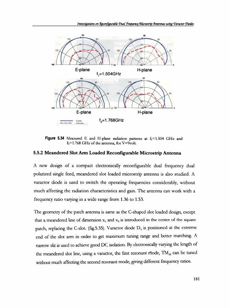
Inzestfgatibns on Qaconfigurabk fluafjfrequenay Mitranfipfllrzwmas usizg ‘Varactor 1)io&s
90 90
/_,lf;~<;j’/i -P ;‘\iI._y \\150 v _ 30 150/’ *. ‘ , \,~<cl 1" ,~‘ \ - 1 ~.r’ K HI 1'iao I ,v ’E-plane H-plane
f1=1 .504G Hz
$\to / Q:Erii
90 90if "‘~t.:190 ~- 0 180 ‘ ¢ ‘ 0E-plane H-plane
Figure 5.34 Measured E and H-plane radiation patterns at f1=1.5O4 GHz andf2=1.768 GHz of the antenna, for V=9volt.
5.5.2 Meandered Slot Arm Loaded Reconfigurable Microstrip Antenna
A new design of a compact electronically reconfigurable dual frequency dual
polarized single feed, meandered slot lo d da e microstrip antenna is also studied. A
varactor diode is used to switch the operating frequencies considerably, without
much affecting the radiation characteristics and gain. The antenna can work with a
frequency ratio varying in a wide range from 1.36 to 1.53.
The geometry of the patch antenna is same as the C-shaped slot loaded design, except
that a meandered line of dimension x1 and x2 is introduced in the center of the square
patch, replacing the C-slot. (fig.5.35). Varactor diode D1 is positioned at the extreme
end of the slot arm in order to get maximum tuning range and better matching. A
narrow slit is used to achieve good DC isolation. By electronically varying the length of
the meandered slot line, using a varactor, the first resonant rfiode, TM“, can be tuned
without much affecting the second resonant mode, giving different frequency ratios.
181
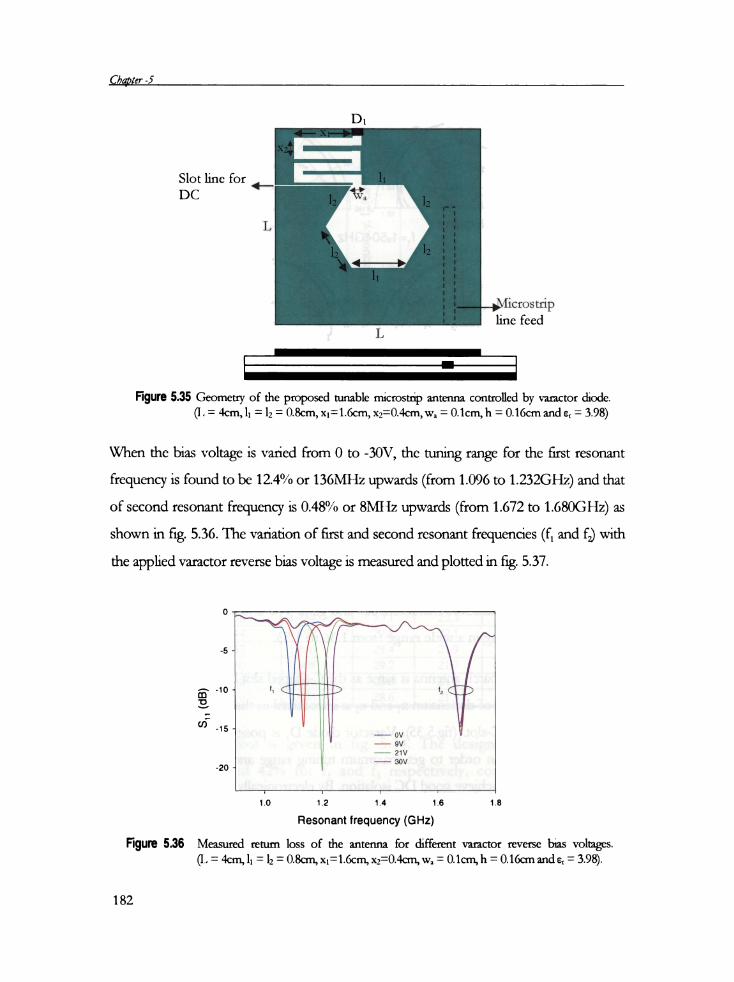
Cbqfier -5
MR1
Slot line forDC ‘L
_fl/Iicrostripline feed
L
Figure 5.35 Geometry of the proposed tunable microsttip antenna controlled by varactor diode.(I. I 4cm, 11 I 12 I O.8cm, x1I1.6cm, x2IO.4cm,W. I O.1cm, h I O.16cm and e, I 3.98)
When the bias voltage is varied from O to -30V, the range for the first resonant
frequency is found to be 12.4% or 136MHz upwards (from 1.096 to 1.232GHz) and that
of second resonant frequency is 0.48% or 8MHz upwards (from 1.672 to 1.68OGHz) as
shown in fig. 5.36. The variation of first and second resonant frequencies (fl and fl) with
the applied varactor reverse bias voltage is measured and plotted in fig. 5.37.
O '~.- .-5- \p h/
‘ r‘IE -10 - l I2
B
c/5’ 45 _ l 1 * 33——— 21V
_20 _k ,5 —— 30VI 1 I l I1.0 1.2 1.4 1.6 1.8Resonant frequency (GHz)
FIQLIIE 5.35 Measured return loss of the antenna for different varactor reverse bias voltages.(L I 4cm, I; I 12 I O.8cm, x1I1.6cm, x2IO.4cm, wa I O.1cm, h I O.16cm and e, I 3.98).
182
Irwe.¢t'gatian.s an Rpcorzfigurafiie Q)ua[f}'requer1cz/1Mi'cro:¢11'pflI:1tzrmas usirg ‘Varactvrflioefis
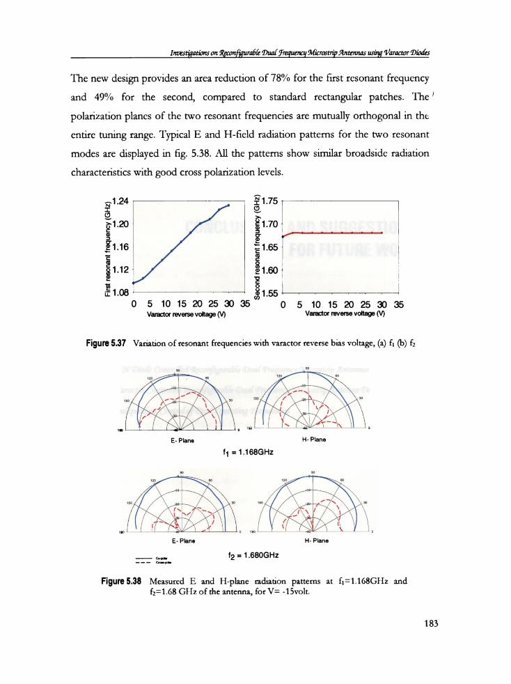
The new design provides an area reduction of 78% for the first resonant frequencyd 49°/ f h 'an 0 or t e second, compared to standard rectangular patches. The
polarization planes of the two resonant frequencies are mutually orthogonal in the
entire tuning range. Typical E and H-field radiation patterns for the two resonant
modes are displayed in fig. 5.38. All the pattems show similar broadside radiation
characteristics with good cross polarization levels.
A124
resonant frequency GHz-5 -L -L5 a E3
&4
1
F'rst
8
Figure 5.37
1 X "
equency GHz.-‘ 1" 1-‘a \l \l01
€l
+
O
r
nd resonan fr
8
j4
l
\
l
Seco.-‘8
G _¢__
5191529253035 05101520253035Varactor reverse voltage (V) VQIBCIOI r6\/BF56 vdlage (V)
Variation of resonant frequencies with varactor reverse bias voltage, (a) fl f2go 90\\\\\ so
/ _P_,w_ , ____ y _-.»"‘-* *"~-~_-_ .r \./_ ~;\ \ / “i",,,“-"“‘5,-\l ~»»,,;_
_ \ ‘/‘;9*__7‘g \ 343 ‘5° / ‘ ‘ i -__g r ‘ \ 30
120, 80 l 20~ , , _- -,_ , » - '~. ,' , 1,r w ‘ ‘‘ V '»_,_‘ 4 , \ ~ /' ‘ 2 i r >_‘4 / i ‘V ._ . \_ //30 V J, ‘x y \ 1 \ \ ,1, r , h _/’ , \li ‘5i"‘~\__ , ii ii’, \ iv l \ Ki ‘l ,9//if Q §l,\ i‘ i|V l‘ ~»i i K» i _ A __ r .e-_.»-Y ‘. l 0
5/ ',?-\ / ‘ g Y»-“.“ X £6 I _‘ \I )-~»_;;j>\ ,____‘r*" /‘X-’ \ y \ lml 1 \ l 1 1,, W L ’E- Plane H- Planef1 = 1 .168GHzso so1 20 “‘\\ so 120 so/it r \ v» 5,/. ‘__);Q_,+_____ \ ,;9_ ;______ ‘i‘ =" i "'~'.__> ‘. I‘ i "*».___ ‘5 ' ' ’ \‘ 30 15 i /‘=”'\ ii so‘ °/_,_ » —-—______/i V if r\ 5 V K
\/I +~ ~/ l t(" 1\ li ‘, I? ii li Ii /i X \ i‘.0 , __, . . _w up“ -, i 0 ‘ac, . 1 i _ A ‘ 'E- Plane H- Plane__ W :2 =1.680GHz——— Cuc-pt
Figure 5.38 Measured E and H-plane radiation patterns at f1=1.168GHz andf;=1.68 GHZ of the antenna, for V= -15volt.
183