Develop a 2.4 Ghz Directional Coupler Using Microstrip Technologies

Jurnal Elektronika dan Telekomunikasi (JET), Vol. 20, No. 2, December 2020, pp. 53-59
Accredited by RISTEKDIKTI, Decree No: 32a/E/KPT/2017
doi: 10.14203/jet.v20.53-59
Band-Pass Filter Microstrip at 3 GHz Frequency Using
Square Open-Loop Resonator for S-Band Radar
Applications
Rima Anisa Maulidini a, *, M. Reza Hidayat a, Teguh Praludi b a Faculty of Engineering
Universitas Jenderal Achmad Yani
Jl. Terusan Jend. Sudirman, Cibeber, Kec. Cimahi Sel., Kota Cimahi, Jawa Barat 40531
Cimahi, Indonesia b Research Center for Electronics and Telecomunnications
Indonesian Institutes of Sciences
Jl. Sangkuriang, Komplek LIPI Gd. 20, Jl. Cisitu Lama, Dago, Kecamatan Coblong, Kota Bandung, Jawa Barat 40135
Bandung, Indonesia
Abstract
In telecommunication, filters are often used to pass the desired frequency. One of them is the Band-Pass Filter (BPF) which
is passing signals between the upper cut-off frequency and the lower cut-off frequency. This research aims to make a band-pass
filter that can pass 3 GHz frequency with a bandwidth of 200 MHz. This filter is designed with a square open-loop resonator
simulated using Advanced Design System (ADS) software. The filter is made using FR 4-epoxy substrates with a dielectric constant
(𝜀𝑟) of 4.6 and substrate thickness (h) of 1.6 mm. Based on the simulation results obtained in the form of a comparison graph
between the response of magnitude to frequency, it shows that the value of the return loss (S11) parameter of -23.549 dB, insertion
loss (S21) parameter value of -1.397 dB, and a slightly shifted middle frequency of 2.890 GHz. Then for the measurement results
obtained a parameter value return loss (S11) of -16.364 dB, parameter value insertion loss (S21) of -3.561 dB with a center frequency
of 3.185 GHz.
Keywords: bandpass filter, filter, microstrip, square open-loop resonator
I. INTRODUCTION
In a radio communication system, any device which
employs radio wave for its propagation purpose needs a
filter to opt the signal waves it uses. One type of filter
that is often used in telecommunications equipment is a
bandpass filter which is a filter that passes a signal within
a certain range and will reject the frequency signal
outside the specified range [1]. The bandpass filter itself
is grouped into two parts, namely wide-band band-pass
filter and narrow-band band-pass filter.
There are several researches on this area which have
been done before. The first study was conducted to
realize the bandpass filter with a hairpin method that
works at a frequency of 3 GHz [2]. The second study was
conducted to realize a microstrip bandpass filter with an
octagonal hairpin shape that works at a frequency of 2.9
– 3.1 GHz with a resonant frequency of 3 GHz [3]. Then
the third study was carried out by modifying the shape of
the hairpin line with the addition of the Defected Ground
Structure to have a value of 0 at the center frequency of
1.27 GHz [4]. The fourth study was carried out to design
a tight microstrip bandpass filter on a U-shaped resonator
[5]. The fifth study is the Compact Microstrip Dual-Band
bandpass filter on the step resonator impedance for C-
band applications [6].
The purpose of this research is to be able to design
and realize a microstrip bandpass filter using an open-
loop square resonator at a frequency of 3 GHz with a
bandwidth of 200 MHz so that it can work at a frequency
of 2900 MHz to 3100 MHz which can be applied to S-
band radar and can produce desired values of return loss
and insertion loss.
II. DESIGN OF THE FILTER
One important thing in making filters with
microstrip media is determining the shape of the
resonator to be used. In general, a resonator is a media
that connects a source port with a load port.
A. Flowchart
In the process, the bandpass filter that is made has
several stages as shown in Figure 1. The first step is
determining the filter specification which includes filter
frequency, filter bandwidth, filter resonator shape, the
dimensions of the filter, and the substrate that will be
used in the filter manufacturing.
The next one is the process of designing a square
open-loop resonator made in the Advanced Design
System (ADS) software along with the simulation of the
design until the resonator design produces an output
value of return loss and insertion loss as needed.
However, when the results are not suitable, re-design, or
re-modification of the design should be carried out until
the results are obtained according to the needs. After the
results are correct, the design will be brought to the
* Corresponding Author.
Email: [email protected]
Received: August 10, 2020 ; Revised: October 02, 2020
Accepted: November 02, 2020 ; Published: December 31, 2020
2020 PPET - LIPI
25-32

54 Rima Anisa Maulidini, et. al.
p-ISSN: 1411-8289; e-ISSN: 2527-9955
process of making a prototype of the square open-loop
bandpass filter microstrip.
After that is the process of measuring the prototype
filter that has been realized. Later, analyzing the results
of the simulation and measurement of the filter to obtain
a return loss and insertion loss value from the simulation
results and the measurement results.
B. Square Open-Loop Resonator
A resonator will resonate at a certain frequency, then
with the existence of that resonance, an RF wave will be
channeled. In general, a resonator circuit can be made
using inductors (L) and capacitors (C) and the magnitude
of the resonant frequency between the circuit L and C is
equal to 1
ω√𝐿𝐶 [7]. There are various kinds of materials
and manufacturing technologies for making filters, one
of which is the LC filter, which is a lumped element filter,
then a planar filter, a coaxial filter, and a dielectric filter.
LC filters are the simplest and have the smallest filter
sizes, but the quality factor is so low that their
performance will be poor. Planar filters are filters that are
quite simple and easy to make [8].
Start
End
Determine filter specifications
(frequency, bandwidth,
resonator dimensions, resonator
shape and substrate)
Square open-loop resonator design
Simulation using
Advance Design System
Software
Change in the size
of the resonator
dimensions
Change in the
size of the
resonator gap
Change in size
and feed
position
simulation results
according to your
needs?
Realization of the
bandpass filter prototype
Bandpass filter measurement
Analysis of simulation
results and measurement and
reporting
No
Yes
Figure 1. Flowchart
C. Microstrip Structure
In the design with microstrip media, the components
L and C are realized using the form of a square open-loop
resonator by bending a single straight resonator into a
square, as shown in Figure 2. By bending it 90° will form
a gap between the two ends of the resonator. So that the
two of the ends of the resonator will form a capacitor that
can store capacitance energy. Theoretically, for a
resonator to resonate at the desired frequency, the length
of a resonator must be ½ the wavelength [9].
The general structure of the microstrip is illustrated
in Figure 3. The transmission line in the microstrip
consists of a conductor strip of width W and thickness t
and a ground-plane conductor at the bottom separated by
a dielectric substrate having a dielectric constant of 𝜀𝑟
and thickness h [10].
D. FR 4-epoxy Substrate
FR 4-epoxy substrate has several material
arrangements, at the very top there is a layer of air as the
outer portion of the substrate, then the yellow layer at the
top of the substrate is a copper conductor material that
functions as a resonator path with a thickness (t) 0.035
mm, in the next section, the FR 4 layer with a dielectric
constant (𝜀𝑟) is used, which is 4.6 with a thickness (h) of
1.6 mm, and the bottom part is the ground plane which is
a conductor made of copper.
In this design, the FR 4 substrate is used as the
material for making the band-pass filter. FR 4-epoxy
substrate is most often used as an electrical insulator
which has considerable mechanical strength because it
has a non-zero air absorption rate. This FR 4 or Flame
Resistant 4 substrate is also a fiberglass matting that
serves with epoxy resin. FR 4 has low water absorption,
good insulation property, and can withstand heat
temperatures up to 140 degrees Celsius.
Figure 2. ½ 𝜆𝑔 Square Open-loop Resonator Design : (a) Single
Straight Resonator, (b) Single Straight Double Resonators Bent 90°
Facing Each Other.
Figure 3. Substrate FR 4

Band-Pass Filter Microstrip at 3 GHz Frequency using Square Open-Loop Resonator for S-Band Radar Applications 55
JURNAL ELEKTRONIKA DAN TELEKOMUNIKASI, Vol. 20, No. 2, December 2020
E. Wavelength Calculation
In resonator design, to determine a frequency, the
length of the resonator is made with a length of ½λg. This
calculation uses the exact formula of Hammerstad and
Jensen [11] as in (1).
𝜆𝑔 =300
𝑓(𝐺𝐻𝑧)√𝜀𝑟𝑒𝑓𝑓 mm (1)
From (1), 𝜆𝑔 is the wavelength or length of the
resonator transmission line, which later the results of
these calculations are used in the design of the resonator
shape as the reference length of the square open-loop
resonator where the frequency is gigahertz and the
effective dielectric constant is calculated as in (2).
F. Effective Dielectric Constant Calculation
The relative dielectric constant of the dielectric
constant can be considered as a homogeneous medium
and substrate replacement air medium. In (2), 𝜀𝑟𝑒𝑓𝑓 is the
effective dielectric constant of the type of substrate used,
namely FR 4, with the variable 𝜀𝑟 as the substrate
dielectric constant, and the variables a and b in (2) are in
(3) and (4).
𝜀𝑟𝑒𝑓𝑓 =𝜀𝑟+1
2+
𝜀𝑟−1
2(1 +
10
𝑢)
−𝑎.𝑏
(2)
𝑎 = 1 +1
49𝑙𝑛 [
𝑢4+(𝑢
52)
2
𝑢4+0.432] +
1
18.7𝑙𝑛 [1 + (
𝑢
18.1)
3
] (3)
𝑏 = 0.564 (𝜀𝑟−0.9
𝜀𝑟+0.3)
0.053
(4)
III. FABRICATION, MEASUREMENT, AND
DISCUSSION
Calculation of the input channel width of the FR4-
epoxy material with 𝜀𝑟 = 4.6 and 𝑍0 = 50Ω, where the
equation approach for W/h is W for microstrip width and
h for microstrip dielectric medium thickness. For the feed
line width at the resonator, (5) is used as the initial design
reference. To determine a frequency, the length of the
resonator is made with a length of ½ 𝜆𝑔 using (1) with the
effective dielectric constant using (2).
For parameter u in (2) and (3) is the data from the
result of (5) with two conditions, namely when u = W/h
≤ 2 and u = W/h > 2. These results will later be used as
an initial determinant of the design length and width in
making the band-pass filter resonator in ADS software. It
can be seen that there are two parameters for each
dimension whose values are different. Because the size
of the resonator to be made is desired to have a small size,
the value of the W/h ≤ 2 is taken which can be seen in
Table 1.
TABLE 1
RESONATOR SIZE BASED ON THE CALCULATION
Parameter Transmission line dimensions (mm)
Length (L) Width (W)
W/h ≤ 2 53.89 2.97
W/h > 2 51.91 4.69
A. Resonator Width Calculation
The calculation of the input channel width of the FR
4-epoxy material with 𝜀𝑟= 4.6 and 𝑍0 = 50 Ω, A is the
variable that needs to be calculated first to complete (5)
where the equation approach for W/h, namely W for the
microstrip width and h for the microstrip dielectric
medium, is obtained from Wheeler [12] and Hammerstad
[13] as in (6).
𝑊
ℎ=
8𝑒𝐴
𝑒2𝐴−2 (5)
A = 𝑍0
60[
𝜀𝑟 +1
2]
0.5
+ 𝜀𝑟−1
𝜀𝑟 +1 [0.23 +
0.11
𝜀𝑟] (6)
B. Design Specifications
As in Table 2, the bandpass filter work at a frequency
between 2.90 GHz – 3.10 GHz with a center frequency
of 3.00 GHz, a bandwidth of 200 MHz using microstrip
technology with a resonator form, namely square open-
loop. In determining the specifications for this bandpass
filter, it is found that by having a resonant frequency of 3
GHz and a BW of 200 MHz, the filter that will be
produced is a narrow-band bandpass filter.
The minimum return loss value is -13.979 dB based
on the conversion of return loss versus voltage standing
wave ratio (VSWR) where when the VSWR is at a value
of 1.50 [14] because when the VSWR value has exceeded
1.50, it causes half of the power loss and the results of the
response will be unfavorable. Therefore, according to
Table 2, the value of the return loss (S11) parameter that
must be generated is at least -10 dB to get bigger results,
so that at the time of transmission, the power is reflected
as little as possible, this will affect the output.
C. Resonator Design Layout for Simulation
The resonators in Figure 4 are made facing each
other which is separated by a gap between the two ends
of the resonator as in Figure 2 which shows a gap with a
predetermined distance so that the parameter values that
will be generated can reach a good state. The band-pass
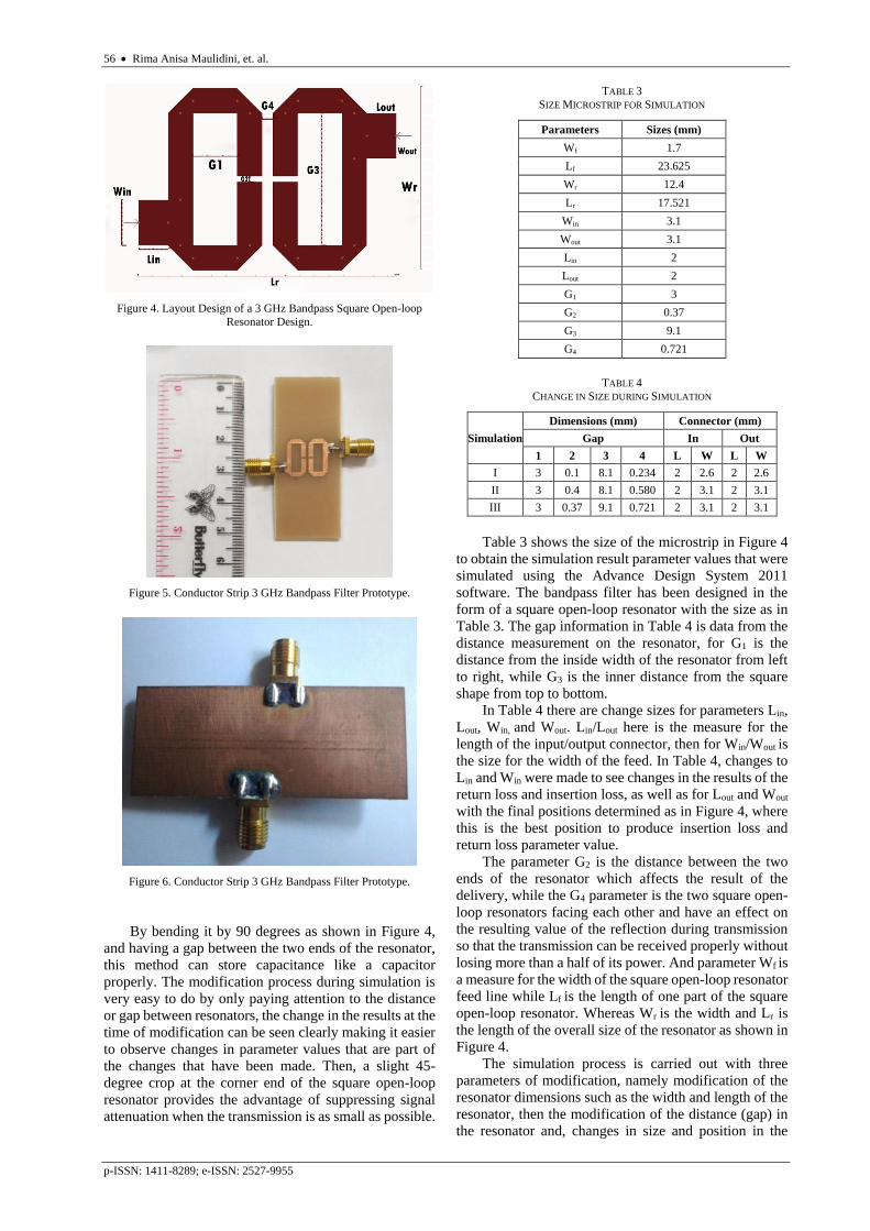
filter prototype realized in Figure 5 is the upper layer of
the substrate, namely the conductor strip that has gone
through a design fabrication process with etching sizes as
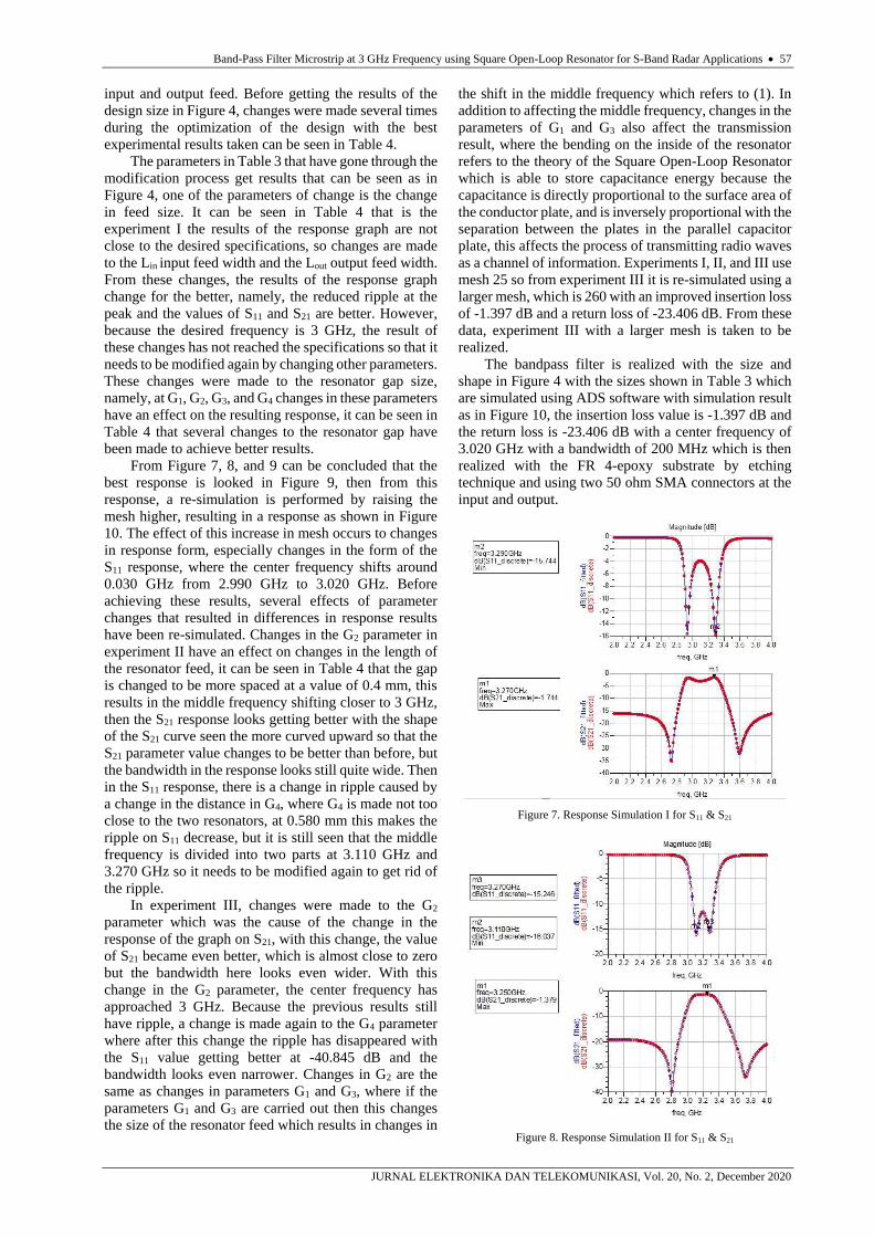
shown in Table 3. Whereas Figure 6 is a part of the
ground plane substrate with an additional 2 cm distance
up and down from the conductor etching strip.
TABLE 2
BAND-PASS FILTER SPECIFICATIONS
Parameters Value
Carrier Frequency (fc) 3 GHz
Range Frequency 2.9 GHz – 3.1 GHz
Bandwidth 200 MHz
Return Loss (RL) Minimum -10 dB
Insertion Loss (IL) Maximum -3 dB
56 Rima Anisa Maulidini, et. al.
p-ISSN: 1411-8289; e-ISSN: 2527-9955
Figure 4. Layout Design of a 3 GHz Bandpass Square Open-loop
Resonator Design.
Figure 5. Conductor Strip 3 GHz Bandpass Filter Prototype.
Figure 6. Conductor Strip 3 GHz Bandpass Filter Prototype.
By bending it by 90 degrees as shown in Figure 4,
and having a gap between the two ends of the resonator,
this method can store capacitance like a capacitor
properly. The modification process during simulation is
very easy to do by only paying attention to the distance
or gap between resonators, the change in the results at the
time of modification can be seen clearly making it easier
to observe changes in parameter values that are part of
the changes that have been made. Then, a slight 45-
degree crop at the corner end of the square open-loop
resonator provides the advantage of suppressing signal
attenuation when the transmission is as small as possible.
TABLE 3
SIZE MICROSTRIP FOR SIMULATION
Parameters Sizes (mm)
Wf 1.7
Lf 23.625
Wr 12.4
Lr 17.521
Win 3.1
Wout 3.1
Lin 2
Lout 2
G1 3
G2 0.37
G3 9.1
G4 0.721
TABLE 4
CHANGE IN SIZE DURING SIMULATION
Simulation
Dimensions (mm) Connector (mm)
Gap In Out
1 2 3 4 L W L W
I 3 0.1 8.1 0.234 2 2.6 2 2.6
II 3 0.4 8.1 0.580 2 3.1 2 3.1
III 3 0.37 9.1 0.721 2 3.1 2 3.1
Table 3 shows the size of the microstrip in Figure 4
to obtain the simulation result parameter values that were
simulated using the Advance Design System 2011
software. The bandpass filter has been designed in the
form of a square open-loop resonator with the size as in
Table 3. The gap information in Table 4 is data from the
distance measurement on the resonator, for G1 is the
distance from the inside width of the resonator from left
to right, while G3 is the inner distance from the square
shape from top to bottom.
In Table 4 there are change sizes for parameters Lin,
Lout, Win, and Wout. Lin/Lout here is the measure for the
length of the input/output connector, then for Win/Wout is
the size for the width of the feed. In Table 4, changes to
Lin and Win were made to see changes in the results of the
return loss and insertion loss, as well as for Lout and Wout
with the final positions determined as in Figure 4, where
this is the best position to produce insertion loss and
return loss parameter value.
The parameter G2 is the distance between the two
ends of the resonator which affects the result of the
delivery, while the G4 parameter is the two square open-
loop resonators facing each other and have an effect on
the resulting value of the reflection during transmission
so that the transmission can be received properly without
losing more than a half of its power. And parameter Wf is
a measure for the width of the square open-loop resonator
feed line while Lf is the length of one part of the square
open-loop resonator. Whereas Wr is the width and Lr is
the length of the overall size of the resonator as shown in
Figure 4.
The simulation process is carried out with three
parameters of modification, namely modification of the
resonator dimensions such as the width and length of the
resonator, then the modification of the distance (gap) in
the resonator and, changes in size and position in the
Band-Pass Filter Microstrip at 3 GHz Frequency using Square Open-Loop Resonator for S-Band Radar Applications 57
JURNAL ELEKTRONIKA DAN TELEKOMUNIKASI, Vol. 20, No. 2, December 2020
input and output feed. Before getting the results of the
design size in Figure 4, changes were made several times
during the optimization of the design with the best
experimental results taken can be seen in Table 4.
The parameters in Table 3 that have gone through the
modification process get results that can be seen as in
Figure 4, one of the parameters of change is the change
in feed size. It can be seen in Table 4 that is the
experiment I the results of the response graph are not
close to the desired specifications, so changes are made
to the Lin input feed width and the Lout output feed width.
From these changes, the results of the response graph
change for the better, namely, the reduced ripple at the
peak and the values of S11 and S21 are better. However,
because the desired frequency is 3 GHz, the result of
these changes has not reached the specifications so that it
needs to be modified again by changing other parameters.
These changes were made to the resonator gap size,
namely, at G1, G2, G3, and G4 changes in these parameters
have an effect on the resulting response, it can be seen in
Table 4 that several changes to the resonator gap have
been made to achieve better results.
From Figure 7, 8, and 9 can be concluded that the
best response is looked in Figure 9, then from this
response, a re-simulation is performed by raising the
mesh higher, resulting in a response as shown in Figure
10. The effect of this increase in mesh occurs to changes
in response form, especially changes in the form of the
S11 response, where the center frequency shifts around
0.030 GHz from 2.990 GHz to 3.020 GHz. Before
achieving these results, several effects of parameter
changes that resulted in differences in response results
have been re-simulated. Changes in the G2 parameter in
experiment II have an effect on changes in the length of
the resonator feed, it can be seen in Table 4 that the gap
is changed to be more spaced at a value of 0.4 mm, this
results in the middle frequency shifting closer to 3 GHz,
then the S21 response looks getting better with the shape
of the S21 curve seen the more curved upward so that the
S21 parameter value changes to be better than before, but
the bandwidth in the response looks still quite wide. Then
in the S11 response, there is a change in ripple caused by
a change in the distance in G4, where G4 is made not too
close to the two resonators, at 0.580 mm this makes the
ripple on S11 decrease, but it is still seen that the middle
frequency is divided into two parts at 3.110 GHz and
3.270 GHz so it needs to be modified again to get rid of
the ripple.
In experiment III, changes were made to the G2
parameter which was the cause of the change in the
response of the graph on S21, with this change, the value
of S21 became even better, which is almost close to zero
but the bandwidth here looks even wider. With this
change in the G2 parameter, the center frequency has
approached 3 GHz. Because the previous results still
have ripple, a change is made again to the G4 parameter
where after this change the ripple has disappeared with
the S11 value getting better at -40.845 dB and the
bandwidth looks even narrower. Changes in G2 are the
same as changes in parameters G1 and G3, where if the
parameters G1 and G3 are carried out then this changes
the size of the resonator feed which results in changes in
the shift in the middle frequency which refers to (1). In
addition to affecting the middle frequency, changes in the
parameters of G1 and G3 also affect the transmission
result, where the bending on the inside of the resonator
refers to the theory of the Square Open-Loop Resonator
which is able to store capacitance energy because the
capacitance is directly proportional to the surface area of
the conductor plate, and is inversely proportional with the
separation between the plates in the parallel capacitor
plate, this affects the process of transmitting radio waves
as a channel of information. Experiments I, II, and III use
mesh 25 so from experiment III it is re-simulated using a
larger mesh, which is 260 with an improved insertion loss
of -1.397 dB and a return loss of -23.406 dB. From these
data, experiment III with a larger mesh is taken to be
realized.
The bandpass filter is realized with the size and
shape in Figure 4 with the sizes shown in Table 3 which
are simulated using ADS software with simulation result
as in Figure 10, the insertion loss value is -1.397 dB and
the return loss is -23.406 dB with a center frequency of
3.020 GHz with a bandwidth of 200 MHz which is then
realized with the FR 4-epoxy substrate by etching
technique and using two 50 ohm SMA connectors at the
input and output.
Figure 7. Response Simulation I for S11 & S21
Figure 8. Response Simulation II for S11 & S21

58 Rima Anisa Maulidini, et. al.
p-ISSN: 1411-8289; e-ISSN: 2527-9955
Figure 9. Response Simulation III for S11 & S21
Figure 10. Response S11 and S21 with mesh 260.
The result of hardware measurement can be seen in
Figure 11, where the measurement results are compared
with the simulation results. The result of the
measurement for the insertion loss value is shown by a
dashed red line with a value of -3.561 dB, while the data
obtained from the simulation for insertion loss is shown
with a red line with a value of -1.397 dB. From the two
results between measurement and simulation there is a
difference of 2.164 dB. The return loss value at the time
of measurement is -16.364 dB which can be seen on the
dotted blue line, while the return loss value during the
simulation is -23.406 dB which is shown by the blue
curve line so that there is a difference of 7.185 dB. The
results of the simulation are better when compared to the
measurement results. Comparative data between
simulation and realization can be seen in Table 5.
TABLE 5
SIMULATION AND THE REALIZATION
Parameters Simulation Result Realization Result
fc 3.020 GHz 3.185 GHz
Range Frequency 2.920 – 3.120 GHz 2.985 – 3.285 GHz
Bandwidth 200 MHz 200 MHz
Return Loss -23.406 dB -16.364 dB
Insertion Loss -1.397 dB -3.561 dB
Figure 11. Response S11 and S21 Measurement & Simulation.
From several previous papers, there are some
methods used that are deemed inadequate to produce
good values of insertion loss and return loss. There are
some of the results of the paper look good, but there are
some that show a very significant difference between
simulation, and realization. So, the results can be
considered to be not optimal.
Whereas in this design the results of the simulation
have reached the specifications, as well as in the
measurement, although there is a shift but the differences
of the simulation and measurement look good. For the
size of the resonator that is realized it has a small size so
that it fits the microstrip filter method using a square
open-loop resonator.
The difference in the results for the parameters S11
and S21 is due to changes in material conditions, dielectric
loss, and reliability during simulation and realization.
During the simulation, the material used is ideal. This is
because the ADS software is arranged in such a way that
the materials used are in accordance with the
specifications. Such as the thickness of the material, the
permittivity of the material that has been treated, and the
adjustments with the measuring instrument.
Because the quality of materials sold in the market
may differ from those simulated and in fact on the market
the quality and reliability of the materials provided have
decreased, it can cause differences in results during
realization and simulation. In addition, the etching and
soldering processes also affect the realization results.
CONCLUSION
The 3 GHz microstrip bandpass filter has been
successfully realized with a square open-loop resonator
using a FR 4-epoxy substrate capable of working at a
frequency 3.085 GHz – 3.285 GHz with a bandwidth of
200 MHz for the parameter (S11) return loss of -16.364
dB, (S21) insertion loss -3.561 dB and a center frequency
of 3.185 dB. From the simulation results and
measurement of the band-pass filter, a difference of
7.185 dB is obtained for the return loss parameter (S11)
and a difference of 2.154 dB for the insertion loss
parameter (S21) with the simulation results of the band-
pass filter for the return loss parameter (S11) of -23.549
dB and the value of insertion loss (S21) -1.397 dB with a
center frequency of 3.020 dB. Changes in G1, G2, and G3
are the cause where the resonator dimensions change,

Band-Pass Filter Microstrip at 3 GHz Frequency using Square Open-Loop Resonator for S-Band Radar Applications 59
JURNAL ELEKTRONIKA DAN TELEKOMUNIKASI, Vol. 20, No. 2, December 2020
which also affect the shift in the center frequency.
Because the longer the resonator, the smaller the
frequency, while the shorter the resonator, the greater the
frequency. Changes in parameters G1 and G3 also affect
the transmission results. Whereas changes in G4 result in
changes in the response results of S11 and S21, the change
in distance affects the transmission process from the
transceiver to the receiver to a minimum so as not to lose
a lot of power and a little power that is reflected.
ACKNOWLEDGMENT
This research activity was carried out with a lot of
support and guidance from several parties involved with
this research. Thanks to UNJANI University and
Research Center for Electronics and Telecommunication,
LIPI Indonesia for all the facilities and guidance that has
been provided.
REFERENCES
[1] J. S. Hong, Microstrip Filters for RF/Microwave Applications,
2nd ed. NY: John Wiley & Sons, Inc., 2011.
[2] B. U. Suryaningsih, A. A. Muayyadi, and E. Sulaeman
"Perancangan dan realisasi bandpass filter yang bekerja pada
frekuensi 3 GHz menggunakan metode hairpin," in e-Proc. Eng.,
vol. 4, no. 1, 2017, pp. 492-499.
[3] T. Praludi, Y. Sulaeman, Y. Taryana, and B. E. Sukoco,
"Bandpass filter microstrip using octagonal shape for S-band
radar," in 2017 Int. Conf. Radar Antenna Microw. Electron.
Telecommun., 2017.
[4] D. Adithama, H. Wijanto, Y. Wahyu, "Filter bandpass hairpin
dengan defected ground structure untuk synthetic aperture radar
1.27 GHz," in e-Proc. Eng., vol. 4, no. 3, 2017, p. 3422.
[5] D. A. Letavin, "Bandpass filters on U-shaped resonator," in 19th
Int. Conf. Micro/nanotechnol. Electron Devices EDM 2018, 2018.
[6] M. Khajavi, and M. Shakiba, "Compact microstrip dual-band
bandpass filter using step impedance resonators," in 27th Iranian
Conf. Elect. Eng., 2019.
[7] R. Y. Aditya, and M. Alaydrus, “Perancangan mikrostrip band-
pass filter pada frekuensi 3.3 GHz dengan menggunakan defected
ground structure”, Universitas Mercu Buana, 2016.
[8] A. B. Santiko, Y. S. Amrullah, Y. Wahyu, M. I. Maulana and B.
Setia, “Design and realization of coupled line bandpass filter
using compact structure at frequencies of 3300 MHz – 3400 MHz
for WiMAX application,” Jurnal Elektronika Telekomunikasi vol.
16, no. 1, pp. 11-14, 2016.
[9] N. A. D. Ayuni, A. Atmaja, and K. Wardani, "Rancang bangun
antena mikrostrip circular patch metode array 4 elemen sebagai
penerima TV UHF," Jurnal Ilmu Pengetahuan Teknologi, vol. 2,
no. 1, pp. 22-31, 2018.
[10] Pattimura University Ambon, Proceedings the 4th International
Conference on Basic Sciences 2018: The Development of Sciences
and Technology in Improving Natural and Cultural Resources.
Ambon: Universitas Pattimura Ambon, 2019.
[11] E. Hammerstad and O. Jensen, “Accurate models for microstrip
computer-aided design,” in 1980 IEEE MTT-S Int. Microw. Symp.
Dig., 1980, pp. 407-409.
[12] H. A. Wheeler, “Transmission-line properties of parallel strips
separated by a dielectric sheet”, IEEE Trans. Microw. Theory
Techniques, vol. 13, no. 2, 1965.
[13] E. O. Hammerstad, "Equations for microstrip circuit design," in
1975 5th European Microw. Conf., Germany, 1975.
[14] Mini-Circuits, Appl. Note DG03-111, p. 111.