Institutionen för systemteknik - DiVA portal308111/FULLTEXT01.pdf · Institutionen för...
101
Institutionen för systemteknik Department of Electrical Engineering Examensarbete Low-Power Low-Noise IQ Modulator Designs in 90nm CMOS for GSM/EDGE/WCDMA/LTE Examensarbete utfört i Radioelektronik vid Tekniska högskolan i Linköping av Mattias Johansson, Jonas Ehrs LiTH-ISY-EX--10/4330--SE Linköping 2010 Department of Electrical Engineering Linköpings tekniska högskola Linköpings universitet Linköpings universitet SE-581 83 Linköping, Sweden 581 83 Linköping
Transcript of Institutionen för systemteknik - DiVA portal308111/FULLTEXT01.pdf · Institutionen för...

Institutionen för systemteknikDepartment of Electrical Engineering
Examensarbete
Low-Power Low-Noise IQ Modulator Designs in
90nm CMOS for GSM/EDGE/WCDMA/LTE
Examensarbete utfört i Radioelektronikvid Tekniska högskolan i Linköping
av
Mattias Johansson, Jonas Ehrs
LiTH-ISY-EX--10/4330--SE
Linköping 2010
Department of Electrical Engineering Linköpings tekniska högskolaLinköpings universitet Linköpings universitetSE-581 83 Linköping, Sweden 581 83 Linköping

Low-Power Low-Noise IQ Modulator Designs in
90nm CMOS for GSM/EDGE/WCDMA/LTE
Examensarbete utfört i Radioelektronik
vid Tekniska högskolan i Linköpingav
Mattias Johansson, Jonas Ehrs
LiTH-ISY-EX--10/4330--SE
Handledare: Magnus Nilsson
ST-Ericsson
Henrik Fredriksson
ST-Ericsson
Niklas Karlsson
ST-Ericsson
Examinator: Atila Alvandpour
ISY, Linköpings universitet
Linköping, 19 March, 2010

Avdelning, Institution
Division, Department
Division of Electrical EngineeringDepartment of Electrical EngineeringLinköpings universitetSE-581 83 Linköping, Sweden
Datum
Date
2010-03-19
Språk
Language
Svenska/Swedish
Engelska/English
⊠
Rapporttyp
Report category
Licentiatavhandling
Examensarbete
C-uppsats
D-uppsats
Övrig rapport
⊠
URL för elektronisk version
http://www.ek.isy.liu.se
http://urn.kb.se/resolve?urn=urn:nbn:se:liu:diva-54552
ISBN
—
ISRN
LiTH-ISY-EX--10/4330--SE
Serietitel och serienummer
Title of series, numberingISSN
—
Titel
TitleEffekt- och Brus-Effektiva IQ Modulatorer i 90nm CMOS för GSM/EDGE/WCD-MA/LTE
Low-Power Low-Noise IQ Modulator Designs in 90nm CMOS forGSM/EDGE/WCDMA/LTE
Författare
AuthorMattias Johansson, Jonas Ehrs
Sammanfattning
Abstract
The current consumption of the IQ modulator is a significant part of the totalcurrent consumption of a mobile transmitter platform and reducing it is of greatinterest. Also, as the WCDMA/LTE standards specifies full duplex transmissionsand Tx and Rx are most often using the same antenna, it is crucial to have asolution with low noise generation. Two new proposals have been studied with theaim to reduce the current consumption and noise contribution of the IQ modulator.
A current mode envelope tracking IQM is the first of the studied designs. Thisimplementation lowers the bias currents in the circuit in relation to the amplitudeof the baseband input signals, meaning that a low input amplitude results in alowering of the current consumption. It proves to be very efficient for basebandsignals with a high peak-to-average ratio. Simulations and calculations have shownthat an average current reduction of 56 % can be achieved for an arbitrary LTEbaseband signal.
The second is an entirely new passive mixer design where the baseband voltagesare sequentially copied to the RF node, removing the need for V-to-I conversion inthe mixer which reduces current consumption and noise. Results from simulationshas proven that this design is fully capable of improving both current consumptionas well as the noise levels. With an output power of 4.0 dBm, the power consump-tion was 43.3 mW, including clock generating circuits. This, combined with thefact that the design is small and simple, means that there is definitely a possibilityto replace the present IQM design with a passive mixer.
Nyckelord
Keywords RF, ASIC, Analog Integrated Circuit, IQ Modulator, IQM, CMOS, 90nm, Predis-tortion, Mixer, Envelope Tracking, Direct Conversion


Abstract
The current consumption of the IQ modulator is a significant part of the totalcurrent consumption of a mobile transmitter platform and reducing it is of greatinterest. Also, as the WCDMA/LTE standards specifies full duplex transmissionsand Tx and Rx are most often using the same antenna, it is crucial to have asolution with low noise generation. Two new proposals have been studied with theaim to reduce the current consumption and noise contribution of the IQ modulator.
A current mode envelope tracking IQM is the first of the studied designs. Thisimplementation lowers the bias currents in the circuit in relation to the amplitudeof the baseband input signals, meaning that a low input amplitude results in alowering of the current consumption. It proves to be very efficient for basebandsignals with a high peak-to-average ratio. Simulations and calculations have shownthat an average current reduction of 56 % can be achieved for an arbitrary LTEbaseband signal.
The second is an entirely new passive mixer design where the baseband voltagesare sequentially copied to the RF node, removing the need for V-to-I conversion inthe mixer which reduces current consumption and noise. Results from simulationshas proven that this design is fully capable of improving both current consumptionas well as the noise levels. With an output power of 4.0 dBm, the power consump-tion was 43.3 mW, including clock generating circuits. This, combined with thefact that the design is small and simple, means that there is definitely a possibilityto replace the present IQM design with a passive mixer.
v


Acknowledgments
We want to express our gratitude to the ST-Ericsson supervisors of the thesisproject, Magnus Nilsson, Henrik Fredriksson and Niklas Karlsson and to otherstaff members of the RF ASIC department at ST-Ericsson who have been helpfulwith all the different problems we have encountered. Thanks goes to the exam-iner of the thesis, Atila Alvandpour and to our opponents, Mattias Johansson andRichard Kjerstadius, for improving the quality of the thesis and the report. Fi-nally, we thank our girlfriends, Charlotta and Anna, who had to endure 6 monthsof distance relationship and see us leave for Lund every week.
Thanks for making this thesis work possible!
vii


List of Abbreviations
AM Amplitude Modulation
BER Bit Error Rate
BPSK Binary Phase Shift Keying
CMOS Complementary Metal Oxide Semiconductor
DAC Digital to Analog Converter
EDGE Enhanced Data rates for Global Evolution
FM Frequency Modulation
FWR Full-Wave Rectifier
GMSK Gaussian Minimum Shift Keying
GPRS General Packet Radio Service
GSM Global System for Mobile communications
HB High Band
HSDPA High Speed Downlink Packet Access
HSPA High Speed Packet Access
HSUPA High Speed Uplink Packet Access
IM InterModulation
IMD InterModulation Distortion
IQ In-phase Quadrature phase
IQM In-phase Quadrature phase Modulator
ISSCC International Solid-State Circuits Conference
LB Low Band
LO Local Oscillator
ix

x
LTE Long Term Evolution
MOSFET Metal Oxide Semiconductor Field Effect Transistor
NMOS N-type Metal Oxide Semiconductor
OFDM Orthogonal Frequency-Division Multiplexing
OP OPerational amplifier
OQPSK Offset Quadrature Phase Shift Keying
PA Power Amplifier
PAR Peak to Average Ratio
PM Phase Modulation
PMOS P-type Metal Oxide Semiconductor
PSK Phase Shift Keying
QAM Quadrature Amplitude Modulation
QPSK Quadrature Phase Shift Keying
RF Radio Frequency
Rx Receiver
SAW Surface Acoustic Wave
SC-FDMA Suppressed Carrier Frequency Division Multiple Access
SNR Signal to Noise Ratio
SSB Single Side Band
Tx Transmitter
VGA Variable Gain Amplifier
WCDMA Wideband Code Division Multiple Access

Contents
1 Introduction 1
1.1 Purpose . . . . . . . . . . . . . . . . . . . . . . . . . . . . . . . . . 11.2 Goals . . . . . . . . . . . . . . . . . . . . . . . . . . . . . . . . . . 21.3 Limitations . . . . . . . . . . . . . . . . . . . . . . . . . . . . . . . 21.4 Simulation environment . . . . . . . . . . . . . . . . . . . . . . . . 21.5 Document outline . . . . . . . . . . . . . . . . . . . . . . . . . . . . 3
2 Theory 5
2.1 Analog modulation . . . . . . . . . . . . . . . . . . . . . . . . . . . 52.1.1 Amplitude modulation . . . . . . . . . . . . . . . . . . . . . 62.1.2 Frequency modulation . . . . . . . . . . . . . . . . . . . . . 62.1.3 Phase modulation . . . . . . . . . . . . . . . . . . . . . . . 7
2.2 IQ data . . . . . . . . . . . . . . . . . . . . . . . . . . . . . . . . . 72.3 IQ modulator . . . . . . . . . . . . . . . . . . . . . . . . . . . . . . 82.4 Digital modulation . . . . . . . . . . . . . . . . . . . . . . . . . . . 9
2.4.1 PSK . . . . . . . . . . . . . . . . . . . . . . . . . . . . . . . 102.4.2 GMSK . . . . . . . . . . . . . . . . . . . . . . . . . . . . . . 102.4.3 QAM . . . . . . . . . . . . . . . . . . . . . . . . . . . . . . 11
2.5 PAR . . . . . . . . . . . . . . . . . . . . . . . . . . . . . . . . . . . 122.6 Wireless communication standards . . . . . . . . . . . . . . . . . . 12
2.6.1 GSM (2G) . . . . . . . . . . . . . . . . . . . . . . . . . . . . 132.6.2 GPRS (2.5G) . . . . . . . . . . . . . . . . . . . . . . . . . . 132.6.3 EDGE (2.75G) . . . . . . . . . . . . . . . . . . . . . . . . . 132.6.4 WCDMA (3G) . . . . . . . . . . . . . . . . . . . . . . . . . 132.6.5 HSPA (3.5G) . . . . . . . . . . . . . . . . . . . . . . . . . . 142.6.6 LTE (4G) . . . . . . . . . . . . . . . . . . . . . . . . . . . . 142.6.7 Technical comparisons . . . . . . . . . . . . . . . . . . . . . 14
2.7 Transmitter efficiency . . . . . . . . . . . . . . . . . . . . . . . . . 172.8 Noise . . . . . . . . . . . . . . . . . . . . . . . . . . . . . . . . . . . 17
2.8.1 Thermal noise . . . . . . . . . . . . . . . . . . . . . . . . . 172.8.2 Flicker noise . . . . . . . . . . . . . . . . . . . . . . . . . . 172.8.3 MOSFET noise model . . . . . . . . . . . . . . . . . . . . . 18
2.9 Non-linearity . . . . . . . . . . . . . . . . . . . . . . . . . . . . . . 182.9.1 IM3 . . . . . . . . . . . . . . . . . . . . . . . . . . . . . . . 20
xi

xii Contents
2.10 Predistortion . . . . . . . . . . . . . . . . . . . . . . . . . . . . . . 202.11 SAW-filter . . . . . . . . . . . . . . . . . . . . . . . . . . . . . . . . 21
3 Reference IQM 23
3.1 Environment . . . . . . . . . . . . . . . . . . . . . . . . . . . . . . 233.2 Architecture . . . . . . . . . . . . . . . . . . . . . . . . . . . . . . . 24
3.2.1 Overview . . . . . . . . . . . . . . . . . . . . . . . . . . . . 243.2.2 Amplifier . . . . . . . . . . . . . . . . . . . . . . . . . . . . 263.2.3 Mixer . . . . . . . . . . . . . . . . . . . . . . . . . . . . . . 283.2.4 RC filter . . . . . . . . . . . . . . . . . . . . . . . . . . . . . 31
3.3 Simulations and results . . . . . . . . . . . . . . . . . . . . . . . . 333.3.1 Testbench setup . . . . . . . . . . . . . . . . . . . . . . . . 333.3.2 Power consumption . . . . . . . . . . . . . . . . . . . . . . . 343.3.3 Linearity . . . . . . . . . . . . . . . . . . . . . . . . . . . . 353.3.4 Noise . . . . . . . . . . . . . . . . . . . . . . . . . . . . . . 36
4 Current Mode Envelope Tracking IQM 37
4.1 Theory . . . . . . . . . . . . . . . . . . . . . . . . . . . . . . . . . . 374.2 Implementation . . . . . . . . . . . . . . . . . . . . . . . . . . . . . 38
4.2.1 Rectifier . . . . . . . . . . . . . . . . . . . . . . . . . . . . . 394.2.2 RC filter . . . . . . . . . . . . . . . . . . . . . . . . . . . . . 42
4.3 Simulations and results . . . . . . . . . . . . . . . . . . . . . . . . 454.3.1 Testbench setup . . . . . . . . . . . . . . . . . . . . . . . . 454.3.2 Power consumption . . . . . . . . . . . . . . . . . . . . . . . 474.3.3 Linearity . . . . . . . . . . . . . . . . . . . . . . . . . . . . 484.3.4 Noise . . . . . . . . . . . . . . . . . . . . . . . . . . . . . . 53
5 Direct Voltage IQM 55
5.1 Theory . . . . . . . . . . . . . . . . . . . . . . . . . . . . . . . . . . 555.2 Implementation . . . . . . . . . . . . . . . . . . . . . . . . . . . . . 58
5.2.1 Output stage noise analysis . . . . . . . . . . . . . . . . . . 585.2.2 Mixer dimensioning . . . . . . . . . . . . . . . . . . . . . . 59
5.3 Simulations and results . . . . . . . . . . . . . . . . . . . . . . . . 605.3.1 Testbench setup . . . . . . . . . . . . . . . . . . . . . . . . 605.3.2 Power consumption . . . . . . . . . . . . . . . . . . . . . . . 625.3.3 Linearity . . . . . . . . . . . . . . . . . . . . . . . . . . . . 625.3.4 Noise . . . . . . . . . . . . . . . . . . . . . . . . . . . . . . 635.3.5 Non-overlapping clock signals . . . . . . . . . . . . . . . . . 645.3.6 Simulating with 4PGFD clocking circuit . . . . . . . . . . . 665.3.7 Discussion . . . . . . . . . . . . . . . . . . . . . . . . . . . . 67
6 Predistorted Direct Voltage IQM 69
6.1 Theory . . . . . . . . . . . . . . . . . . . . . . . . . . . . . . . . . . 696.2 Implementation . . . . . . . . . . . . . . . . . . . . . . . . . . . . . 706.3 Simulations and results . . . . . . . . . . . . . . . . . . . . . . . . 71
6.3.1 Testbench setup . . . . . . . . . . . . . . . . . . . . . . . . 716.3.2 Power consumption . . . . . . . . . . . . . . . . . . . . . . . 72
Contents xiii
6.3.3 Linearity . . . . . . . . . . . . . . . . . . . . . . . . . . . . 726.3.4 Noise . . . . . . . . . . . . . . . . . . . . . . . . . . . . . . 736.3.5 Simulating with 4PGFD clocking circuit . . . . . . . . . . . 75
7 Conclusions 77
7.1 Future work . . . . . . . . . . . . . . . . . . . . . . . . . . . . . . . 787.1.1 Envelope Tracking IQM . . . . . . . . . . . . . . . . . . . . 787.1.2 Direct Voltage IQM . . . . . . . . . . . . . . . . . . . . . . 80
7.2 Final words . . . . . . . . . . . . . . . . . . . . . . . . . . . . . . . 81
Bibliography 83


Chapter 1
Introduction
The continued enhancement of wireless technology puts great pressure on thecompanies acting in the field. In the mobile phone industry one can see a globalscurry towards being the first to present the latest technology on the market. Moreand more applications and functions are squeezed into the phones to meet therequirements of the customers. While increasing the size of the phones extensivelyis not an option, more area and power efficient batteries and circuits is the key forobtaining the capabilities needed for new and better functionalities.
In this thesis we examine the IQ modulator for a mobile communication chip,trying to find new ways to reduce the current consumption. Also, as the presentimplementation at ST-Ericsson of the IQ modulator, the Original IQM, has asomewhat high noise floor, it is followed by an expensive SAW (Surface AcousticWave) filter off-chip to reduce the Tx-Rx interference. Constructing an IQ modu-lator that lowers this noise floor would mean that it might be possible to removethis expensive filter and reduce cost and area. The new IQ modulators are de-signed to be able to handle signals from several wireless communication standards,where the focus for this thesis lies on GSM, EDGE, WCDMA and LTE.
1.1 Purpose
The thesis was carried out at ST-Ericsson in Lund, Sweden, with the main focusto analyze and reduce the current consumption of the IQ modulator (see Section2.3), which is a common part in the Tx chain of an RF circuit. The analysisinvolved examining two new IQ modulators and understand their behavioral andperformance.
1

2 Introduction
1.2 Goals
The goals for this thesis are:
• Study and understand the limitations of the following IQ modulator designs:
– Current Mode Envelope Tracking IQ Modulator
– Direct Voltage IQ Modulator
• Compare these two modulators to each other as well as to a slightly modifiedversion of the Original IQM, called the Reference IQM, in the context ofpower consumption, linearity and noise.
1.3 Limitations
• This thesis is concluded on a schematics hierarchy level, not taking circuitlayout complications into concern.
• The IQ modulators in this thesis are designed to work with several mobilecommunication standards and several frequency bands, spanning an outputfrequency range of 700-2500 MHz. However, this thesis is limited to studiesat 2000 MHz.
• To adjust the gain of the Original IQM between 1 dB and 20 dB using1 dB steps, several select signals can be set to logarithmically enable ordisable 70 identical mixer units whose currents adds together to achieve thewanted gain. Throughout the thesis, this variable gain functionality is notimplemented. Instead, simulations have been done using always maximumgain. This equals to enabling all 70 mixer units concurrently.
1.4 Simulation environment
All circuits were constructed in 90 nm CMOS process using Cadence VirtuosoSuite and were simulated using Spectre. Coherently throughout the simulationsa single tone SSB modulated sinusoidal was used as baseband signal. SSB means
that the Q-part of the signal has the same frequency but phase shiftedπ
2from the
I-part as (see Section 2.2 for IQ theory):
I(t) = cos(ω0t) (1.1)
Q(t) = cos(ω0t −π
2) = sin(ω0t) (1.2)

1.5 Document outline 3
These signals linearily mixed in an IQ modulator (Section 2.3), as in Equation 2.9,results in the RF signal:
sRF (t) =I(t) cos(ωct) + Q(t) sin(ωct)
= cos(ω0t) cos(ωct) + sin(ω0t) sin(ωct) (1.3)
=cos[(ωc − ω0)t]
2+
cos[(ωc + ω0)t]
2+
cos[(ωc − ω0)t]
2− cos[(ωc + ω0)t]
2=
=cos[(ωc − ω0)t] (1.4)
The reason for using an SSB modulated sine wave is that many of the specificationsprovided by ST-Ericsson are referred to when using such input. Also, an SSB sinewave is an easy test case because in a linear system it resolves in only one outputfrequency. In simulations, a carrier frequency of 2 GHz was used to cover themost commonly used frequency bands of modern communication standards. Theapplied baseband signal at 10 MHz refers to the case of an LTE signal with a 20MHz bandwidth, creating a wanted frequency at 1990 MHz.
1.5 Document outline
The thesis report is separated into seven chapters and is written for Master ofScience students already familiar with basic signal and electronics theory. Chapter2 covers some basic RF theory sections, including modulation techniques and thefunctionality of a theoretical IQ modulator. The following four chapters, all coversone implemented design each, where Chapter 3 describes a reduced version of theOriginal IQM design, referred to as the Reference IQM. Following in chapters 4-6 are the new implemented ideas, which are called the Envelope Tracking IQM,Direct Voltage IQM and Predistorted Direct Voltage IQM respectively. The lastchapter presents the conclusions and proposed future work.


Chapter 2
Theory
This chapter tries to cover the necessary background theory that is needed for theintended reader to understand the thesis. It includes basic RF theory as analog anddigital modulation as well as descriptions of IQ data and the IQ modulator, as wellas some brief descriptions of some of the mobile communication standards withinthe focus of this thesis. There is also some notes about PAR, transmitter efficiencyand circuit noise and in the end there are short discussions about linearity andpredistortion.
2.1 Analog modulation
The basic principle behind signal modulation is transmitting information by themodification of a typically high frequency carrier wave
sc(t) = Ac cos(ωct + ϕc) (2.1)
where ωc = 2πfc and fc is the carrier frequency. This carrier and its notation willbe used as an example throughout the chapter. This chapter will also use a simpleinput signal, called the modulating signal, sm(t):
sm(t) = Am cos(ωmt + ϕm) (2.2)
where, similar as above, ωm = 2πfm and fm is the modulating signal’s frequency.Sending information using modulation has several advantages. It allows many
transmitters to transmit at the same time by letting every transmission have theirown frequency (or frequency band). It is also easier to construct antennas thatare efficient for higher frequencies than lower, and the higher frequency antennascan be built smaller as well. [3]
All signal modulation schemes are based on three modulation modes; Ampli-tude, Frequency and Phase Modulation. [3]
5

6 Theory
2.1.1 Amplitude modulation
AM is the simplest modulation scheme and was also the first to be used. It isbased on inserting information in the carrier wave’s amplitude. The modulatedAM signal could mathematically be described as: [3]
sAM (t) = Ac[1 + sm(t)] cos ωct (2.3)
Time
Am
plitu
de
Figure 2.1. Example of AM. sm(t) superimposed in red.
2.1.2 Frequency modulation
As far as AM is simple to understand and is rather simple to implement it stillhas it’s drawbacks. The biggest disadvantages is the susceptability to noise andpoor power efficiency. The concept of frequency modulation tries to avoid thisby letting the FM signal not depend on its amplitude, but on its frequency. Themodulated FM signal is given by: [3]
sFM (t) = Ac cos(ωct + 2πf∆
t∫
0
sm(τ)dτ) (2.4)
where f∆ is the frequency deviation, which is the maximum frequency change ofthe carrier wave in one direction. [3]
Time
Am
plitu
de
Figure 2.2. Example of FM. sm(t) superimposed in red.

2.2 IQ data 7
2.1.3 Phase modulation
The third modulation mode is phase modulation, where the phase of the car-rier wave is changed proportionally to the modulating wave’s amplitude. Phasemodulation is given by: [3]
sPM (t) = Ac cos(ωct + sm(t)) (2.5)
Important to notice is that FM and PM are using the same physical property, theangle of sc(t), and therefore they cannot be used simultaneously. This is importantto recognize as it will be discussed later.
Time
Am
plitu
de
Figure 2.3. Example of PM. sm(t) superimposed in red.
2.2 IQ data
It is common in radio communications to discuss the transmitted signal using thetwo-dimensional IQ representation, where I stands for In-phase and Q for Quadra-ture phase. To explain this representation we first look closer at the modulatingwave:
sm(t) = Am cos(ωmt + ϕm︸ ︷︷ ︸
θm
) (2.6)
At any given moment in time, this signal could be represented as a phasor in atwo-dimensional plane (the IQ-plane) using polar coordinates where Am is theamplitude and θm is the angle as shown in Figure 2.4. Looking at that figure it ispretty straightforward to explain IQ which is merely the cartesian coordinates ofthis representation, i.e.
Id = Am cos(θm) (2.7)
Qd = Am sin(θm) (2.8)
However, now one would maybe wonder why going the extra step and transform theperfectly simple polar representation to IQ representation. The answer lies in theperformance of IQ modulator hardware and simplicity in digital signal processing.Constructing a precise phase shifter for high frequencies is difficult, it is easier to

8 Theory
Figure 2.4. Modulating wave as a phasor in the IQ-plane
only adjust the amplitudes of I and Q instead. Also, as we will see in Section 2.4,several digital modulation schemes operate directly on the I and Q components ofthe carrier signal which without an IQ modulator leads to unnecessary conversionin the digital domain from IQ to polar representation. [10]
2.3 IQ modulator
In the IQM the I part of the baseband signal is multiplied with a cosine carrierwave and the Q part is multiplied with a 90 shifted cosine carrier wave, or inother words, a sine carrier wave. Carriers separated by 90 are called quadraturecarriers, or orthogonal carriers. As these two signals are orthogonal they can beadded together without information loss, resulting in the outgoing RF signal. Thetransmitted signal is expressed as: [10]
sRF (t) = I(t) cos(ωct) + Q(t) sin(ωct) (2.9)
Figure 2.5. IQ modulator

2.4 Digital modulation 9
To demodulate this signal, sRF is again multiplied with the same carrier wavesand I and Q can be retreived after lowpass filtering. For example, to retreive theI part again the following multiplication is done
sRF (t) cos(ωct) = I(t) cos2(ωct) + Q(t) cos(ωct) sin(ωct) =
=I(t)
2+
1
2[I(t) cos(2ωct) + Q(t) sin(2ωct)] (2.10)
and then lowpass filtering givesI(t)
2.
Figure 2.6. IQ demodulator
As understood, the IQM is not a modulator associated with a certain modulationscheme, it can actually be used with any modulation scheme. The actual mod-ulation is typically made in the digital domain before being transmitted to theIQM.
2.4 Digital modulation
In digital modulation the information to be sent are digital bits that are com-bined into symbols representing one or more bits. These symbols are commonlytransmitted using a constant symbol rate defined by the communication standardin use. For example, the symbol rate in GSM is 270.833 kilosymbols/sec. Eachsymbol consists of 1 bit which gives a total data rate of 270.833 kbps for speech,data and control signals. This is divided between 8 mobile stations as GSM usestime-division access. [21]
Frequency bandwidth today is restricted by law in most countries. The gov-ernments decide what frequencies are to be allocated for different uses. Thereforea high bandwidth efficiency is wanted when designing wireless communicationstandards. Different modulation techniques with higher and higher bandwidth ef-ficiency have been developed over the years to cope with the growing usage of thefrequency spectrum. Some of these are described in the following sections.

10 Theory
(a) 2-PSK (b) QPSK (c) 8-PSK
Figure 2.7. Popular PSK constellations
2.4.1 PSK
PSK (Phase Shift Keying) is a digital modulation scheme that modulates the phaseof the carrier to transmit digital data. The number of possible phase positionsdefined in PSK can be arbitrary. For example, with 2-PSK there are two possiblephases defined and a transmitter can therefore transmit one bit per symbol, bymodulating the carrier as: [17]
Ac sin(2πfct) , representing digital ’1’ (2.11)
Ac sin(2πfct + π) , representing digital ’0’ (2.12)
Of course, a 2-logarithmic number of possible phases, or states, gives the possibilityto fully encode binary data in these states.
By looking at the IQ plane for PSK we can see the good usage of IQ-data.PSK is using a phase shifting algorithm which is easily realized by changing the Ipart and the Q part of the signal. In figure 2.7 2-PSK, 4-PSK (also called QPSK)and 8-PSK constellations are plotted in the IQ-plane. By using a higher orderPSK more bits can be transmitted per symbol but it is of course more sensibleto interference as noise causes the received signal to not exactly point at a validconstellation position. [3, 17]
Worth mentioning is the OQPSK, which is a QPSK modulation scheme with atime offset between the I and the Q part of half a symbol. By using regular QPSKthere is always the possibility of a 180 phase transition when going from 00 to11, for example. With an offset the I and Q part changes value at different timeswhich leads to a maximum phase transition of 90 not causing the envelope to goto 0 for a short time. This increases the bandwidth efficiency. [13]
2.4.2 GMSK
Another way of representing binary data is to let the direction of a phase shiftrepresent either ’0’ or ’1’ and hold the amplitude of the IQ phasor at a constant
2.4 Digital modulation 11
level. GMSK (Gaussian Minimum Shift Keying) is a modulation technique thatuses this concept when encoding data. The GMSK signal is similar to the oneproduced by OQPSK. The difference is that each one of the square shaped pulsesin OQPSK is replaced with a gaussian filter shaped pulse. Low side lobes and anarrower main lobe is obtained when using the gaussian filter instead of a rect-angular pulse, which results in less interference between frequency channels. Thefrequency response and impulse response of the gaussian filter are described byequation 2.13 and 2.14 respectively. [15,16,25]
H(f) = e−(f/a)2 (2.13)
h(t) =√
πae−(πat)2 (2.14)
The constant a determines the 3dB bandwidth B of the filter according toequation 2.15. [25]
B = a
√
ln√
2 (2.15)
2.4.3 QAM
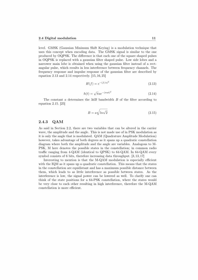
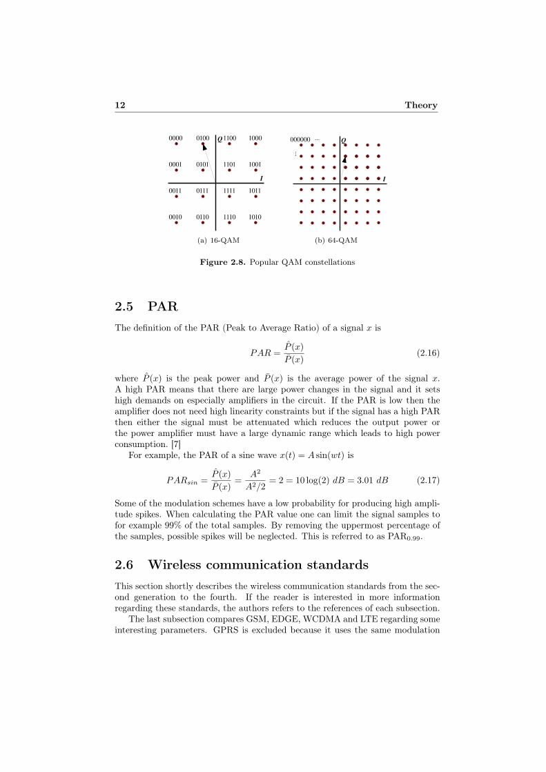
As said in Section 2.2, there are two variables that can be altered in the carrierwave, the amplitude and the angle. This is not made use of in PSK modulation asit is only the angle that is modulated. QAM (Quadrature Amplitude Modulation)however, takes advantage of both degrees as it spans up a quadratic constellationdiagram where both the amplitude and the angle are variables. Analogous to M-PSK, M here denotes the possible states in the constellation; in common radiotraffic ranging from 4-QAM (identical to QPSK) to 64-QAM. In 64-QAM everysymbol consists of 6 bits, therefore increasing data throughput. [3, 13,17]
Interesting to mention is that the M-QAM modulation is especially efficientwith the IQM as it spans up a quadratic constellation. This means that the statesin the constellation are equidistant and has a maximum possible distance betweenthem, which leads to as little interference as possible between states. As theinterference is low, the signal power can be lowered as well. To clarify one canthink of the state positions for a 64-PSK constellation, where the states wouldbe very close to each other resulting in high interference, therefore the M-QAMconstellation is more efficient.
12 Theory
(a) 16-QAM (b) 64-QAM
Figure 2.8. Popular QAM constellations
2.5 PAR
The definition of the PAR (Peak to Average Ratio) of a signal x is
PAR =P (x)
P (x)(2.16)
where P (x) is the peak power and P (x) is the average power of the signal x.A high PAR means that there are large power changes in the signal and it setshigh demands on especially amplifiers in the circuit. If the PAR is low then theamplifier does not need high linearity constraints but if the signal has a high PARthen either the signal must be attenuated which reduces the output power orthe power amplifier must have a large dynamic range which leads to high powerconsumption. [7]
For example, the PAR of a sine wave x(t) = A sin(wt) is
PARsin =P (x)
P (x)=
A2
A2/2= 2 = 10 log(2) dB = 3.01 dB (2.17)
Some of the modulation schemes have a low probability for producing high ampli-tude spikes. When calculating the PAR value one can limit the signal samples tofor example 99% of the total samples. By removing the uppermost percentage ofthe samples, possible spikes will be neglected. This is referred to as PAR0.99.
2.6 Wireless communication standards
This section shortly describes the wireless communication standards from the sec-ond generation to the fourth. If the reader is interested in more informationregarding these standards, the authors refers to the references of each subsection.
The last subsection compares GSM, EDGE, WCDMA and LTE regarding someinteresting parameters. GPRS is excluded because it uses the same modulation

2.6 Wireless communication standards 13
as GSM. HSPA is basically an earlier form of LTE and is therefore also excluded.The main difference for the purpose of this thesis is that LTE can use 64-QAM inthe uplink, which is from mobile to base station, and HSPA can not.
2.6.1 GSM (2G)
A certain band in the frequency spectrum is allocated for the GSM standard tobe used for communication between mobile stations and base stations. Withinthis spectrum there are 124 discrete frequency carriers defined, where each car-rier is partitioned into 8 time-divided slots. In total this gives 124 ∗ 8 = 992available traffic channels within each radio cell to be distributed among users.When transmitting data over these channels, GSM uses the modulation techniqueGMSK. [23]
2.6.2 GPRS (2.5G)
A big step in the evolution towards the third generation of telecommunicationstandards was GPRS, often referred to as 2.5G to show the link between 2G and3G. GPRS introduces a packet-switched network, which still uses the GSM networknodes along with some additional GPRS specific nodes, to handle the transport ofpacket data. The modulation technique used for GPRS is GMSK, the same as forGSM. [4, 20]
2.6.3 EDGE (2.75G)
Further improvement of the GSM technology was made when implementing EDGE.By introducing the modulation technique 8-PSK, EDGE is able to transfer 3 bitsper symbol compared to the 1 bit per symbol of the GMSK technique used byGSM and GPRS. This leads to a higher data throughtput even though the band-width is the same. A drawback is that 8-PSK is more sensitive to noise due tothe shorter distance between the states in the constellation diagram (see Figure2.7). To solve this problem, EDGE switches from 8-PSK to GMSK when the SNRbecomes to low, e.g. when the user is located near the edge of a radiocell. [18]
2.6.4 WCDMA (3G)
To achieve a high data throughput WCDMA (Wideband Code Division Multi-ple Access) uses a wide frequency bandwidth where the user data is spread bymultiplying it with quasi-random bits which are derived from orthogonal CDMAspreading codes. By adding these CDMA codes to the signals, it is possible formultiple users to transmit at the same frequency at the same time.
Just as GSM, WCDMA uses a combination of time and frequency division witha 5 MHz separation between the carrier frequencies. For modulation of the uplinkdata WCDMA uses QPSK. [8]
14 Theory
2.6.5 HSPA (3.5G)
HSDPA is a protocol for transfering data from the base station to the mobilestation. Among other improvements over WCDMA it uses adaptive modulationthat initially uses QPSK but if the signal quality is good it can improve data ratesby using 16-QAM or 64-QAM. [5]
In addition to the downlink protocol, HSUPA was released to manage theuplink traffic and as a pair they are commonly called HSPA. HSUPA is using thesame adaptive modulation technique as HSDPA, except that it can not use 64-QAM. Some extra overhead information about e.g. power control and schedulingare embedded in the data sent from the mobile station to the base station, as onewants to minimize the amount of calculations made in the mobile. This informationis handled by the base station instead. [5]
2.6.6 LTE (4G)
In the downlink LTE uses another access technique called OFDM to increase thespectral efficiency. With this, the information in an assigned band is divided ontoseveral subcarriers, 15 kHz apart, all orthogonal to each other. This increasesspectral efficiency as the subcarriers can be placed close to each other. In theuplink, to reduce the PAR, a similar technique called SC-FDMA is used, whichalso uses orthogonal subcarriers but transmits the data sequentially instead of inparallel. [9]
As in WCDMA/HSPA different modulation techniques are used in the uplinkdepending on the condition of the link, but the choice of modulation techniquesis wider. LTE can switch between QPSK, 16-QAM and 64-QAM. The bandwidthof LTE can vary between 1.4 and 20 MHz. [1, 19]
2.6.7 Technical comparisons
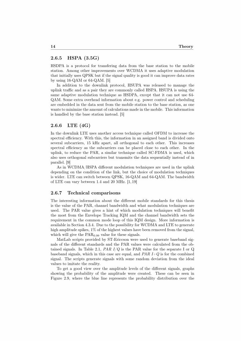
The interesting information about the different mobile standards for this thesisis the value of the PAR, channel bandwidth and what modulation techniques areused. The PAR value gives a hint of which modulation techniques will benefitthe most from the Envelope Tracking IQM and the channel bandwidth sets therequirement in the common mode loop of this IQM design. More information isavailable in Section 4.3.4. Due to the possibility for WCDMA and LTE to generatehigh amplitude spikes, 1% of the highest values have been removed from the signal,which will give the PAR0.99 value for these signals.
MatLab scripts provided by ST-Ericcson were used to generate baseband sig-nals of the different standards and the PAR values were calculated from the ob-tained signals. In Table 2.1, PAR I/Q is the PAR value for the separate I or Qbaseband signals, which in this case are equal, and PAR I+Q is for the combinedsignal. The scripts generate signals with some random deviation from the idealvalues to imitate the reality.
To get a good view over the amplitude levels of the different signals, graphsshowing the probability of the amplitude were created. These can be seen inFigure 2.9, where the blue line represents the probability distribution over the

2.6 Wireless communication standards 15
Standard Modulation PAR I/Q PAR I+Q Channel bandwidthGSM GMSK 3.03 0.00 200 kHzEDGE 8-PSK 6.24 3.29 200 kHzWCDMA QPSK 5.03 3.54 5 MHzLTE 64-QAM 8.39 5.39 20 MHz
Table 2.1. Technical data of wireless standards [1, 2, 6]
amplitude and the dashed red line shows the cumulative probability. The graphsshow the probability distributions for the I baseband signals, which have the sameamplitude probabilities as the Q baseband signals, with a minimum amplitude of0 V and a maximum of 300 mV.
16 Theory
Pro
bability
(%)
Amplitude mVGSM (GMSK)
Cum
ula
tive
Pro
b.
(%)
0 50 100 150 200 250 3000
50
100
0
1.1
2.2
Pro
bability
(%)
Amplitude mVEDGE (8-PSK)
Cum
ula
tive
Pro
b.
(%)
0 50 100 150 200 250 3000
50
100
0
1.1
2.2
Pro
bability
(%)
Amplitude mVWCDMA (QPSK)
Cum
ula
tive
Pro
b.
(%)
0 50 100 150 200 250 3000
50
100
0
1.1
2.2
Pro
bability
(%)
Amplitude mVLTE (64-QAM)
Cum
ula
tive
Pro
b.
(%)
0 50 100 150 200 250 3000
50
100
0
1.1
2.2
Figure 2.9. Amplitude probability distribution of I/Q baseband signals

2.7 Transmitter efficiency 17
2.7 Transmitter efficiency
A value that is useful when doing circuit comparisons in RF with the aim todecrease power consumption is the transmitter efficiency. It is defined as
Transmitter efficiency =Transmitted power
Consumed DC power(2.18)
The value tells us how much of the input DC power is actually fed to the antenna.The power not fed to the antenna generates unnecessary heat, which is importantto reduce as it must be transported away with expensive heatsink solutions. [3]
2.8 Noise
Noise in electrical circuits can be divided into two groups, interference noise andinherent noise. Interference noise is noise originating from other sources than theobserved circuit, such as noise on a power supply line or electromagnetic interfer-ence from other circuits nearby. Inherent noise is the noise that the circuit itselfgenerates. This noise is a variable that could be reduced by proper schematic andlayout design. The following sections describes the main causes of inherent noisein a MOSFET transistor. [11]
A definition of a noise source’s voltage spectral density would also be in or-der. The voltage spectral density function, V 2
n (f), or I2n(f), is a function of the
average power at a certain frequency. Fact is that many noise sources are fre-quency dependent so this is crucial for calculations of the total noise at a certainbandwidth. [11]
2.8.1 Thermal noise
Thermal noise is generated by the thermal excitation of the charged carriers in aconductor. The noise is proportional to the absolute temperature of the conductorand is independent of the frequency, i.e. the spectral density is constant. [11]
For example, the noise in a resistor is primarily thermal noise and its voltagespectral function is:
V 2r (f) = 4kBTR (2.19)
where kB is Boltzmann’s constant, T is absolute temperature and R is the resis-tance. [11]
2.8.2 Flicker noise
Flicker noise is also called 1/f noise because it is inverse proportional to thefrequency. It usually comes from ’traps’ in the component where carriers get stuckfor some period of time and then is released. Its spectral density can be written:
V 2n (f) =
k2v
f(2.20)
where kv is a constant. [11]

18 Theory
Figure 2.10. Noise model of a MOSFET in saturation
2.8.3 MOSFET noise model
The inherent noise from a MOSFET is mainly thermal noise and flicker noise.The thermal noise is easy to understand as it directly originates from the resistivechannel of a MOSFET. In ohmic mode the thermal noise is easily described by
V 2d (f) = 4kBTrDS ⇒ I2
d(f) =4kBT
rDS(2.21)
where rDS is channel resistance. However, when the transistor enters active modethe channel cannot be described homogenous any longer. The thermal noise isthen more accurately approximated by: [11]
I2d(f) = 4kBT
(2
3
)
gm (2.22)
The flicker noise in a MOSFET is modeled as a voltage source connected inseries with the gate:
V 2g (f) =
K
WLCoxf(2.23)
where K is dependent on physical characteristics of the device, W is transistorwidth, L length and Cox is gate capacitance per unit area. Worth noting is thatp-channel transistors have typically less flicker noise because the carriers (holes)are less likely to be trapped. In Figure 2.10 the total noise model of a MOSFETin active mode is shown. [11]
2.9 Non-linearity
A non-linear transfer function in an RF transmitter degrades not only its ownspectra but also the adjacent channels, interfering others transmissions. Unfor-tunately, all electrical systems are somewhat non-linear because of the physicallimitations of the components. Thus, for accurate calculations the system needsto be modeled using a non-linear model. The output of a non-linear system canbe modeled as an infinte polynomial expression,
y(t) = α1x(t) + α2x2(t) + α3x
3(t) + ... (2.24)
where y(t) is the output signal, x(t) is the input signal and αi are constants.

2.9 Non-linearity 19
The property of non-linearity in a circuit can be observed in different ways.One way is the occurrence of harmonics in the output signal when having a periodicinput signal. One easy example is to let the input signal to a third order systembe x(t) = cos(ωt), then the output signal will be
y(t) = α1 cos(ωt) + α2 cos2(ωt) + α3 cos3(ωt)
=α2
2+ (α1 +
3α3
4) cos(ωt) +
α2 cos(2ωt)
2+
α3 cos(3ωt)
4(2.25)
As seen these harmonics can be found at multiples of the input frequency andtherefore they can rather easily be attenuated using filtering.
Another way to discover and measure non-linearities is to measure the in-termodulation products. Intermodulation products occur when the input signalcontains more than one frequency. These multiple frequencies now modulates withthemselves, simplest seen with an input of x(t) = cos(ω1t) + cos(ω2t), again in athird order system:
y(t) =α1[cos(ω1t) + cos(ω2t)] +
α2[cos(ω1t) + cos(ω2t)]2+
α3[cos(ω1t) + cos(ω2t)]3 (2.26)
This expression expands to the expression visualized by the following table:
Angular frequency Amplitude
0 α2
ω1 α1 + 94α3
ω2 α1 + 94α3
2ω112α2
2ω212α2
ω1 ± ω2 α2
2ω1 ± ω234α3
2ω2 ± ω134α3
3ω114α3
3ω214α3
Table 2.2. Intermodulation products in a third order system
When ω1 and ω2 are close to each other in frequency the problem with inter-modulation are the components 2ω1 − ω2 and 2ω2 − ω1, which are close to theinput frequencies and thus hard to filter out using filtering. The calculations alsoreveals that the main problem is the third order non-linearity, the second orderonly creates unwanted components at much higher (or lower) frequencies thatare easier to filter out. In fact, when calculating with higher order systems than

20 Theory
three it can be seen that all even order non-linearites creates components that areeasy to filter out. That means that the intermodulation problem is the odd ordernon-linearities. [14]
2.9.1 IM3
In this thesis the measure for non-linearities is the third order intermodulationdistortion, IM3 (or IMD3) of an SSB baseband signal. With a single tone simula-tion in an IQ modulator as this, the IM3 is attained from a harmonic folding backto the in-band such as:
• First the third harmonic of the LO signal, 3ωc, is mixed with the fundamentaltone in the baseband signal, ωm, creating the unwanted harmonic signal3ωc +ωm (the 3ωc −ωm is not created because the third harmonic of the LOsignal is phase shifted 180).
• In the mixing process also the wanted frequency is created, ωc − ωm.
• These two components are now intermodulated, effectively folding back acomponent, (3ωc + ωm)− 2(ωc − ωm) = ωc + 3ωm. This occurs in-band andis very important to reduce with an as linear system as possible.
2.10 Predistortion
Predistortion refers to the deliberate introduction of a non-linearity - a predistor-tion - to a signal, before it is being applied to a system, with the aim to compensatefor the systems own non-linearities. The transfer function of the predistortion mustthen be as close as possible to the opposite of the transfer function of the system.To illustrate, an amplifier with a transfer characteristic of the one in Figure 2.11(a)can be compensated with a predistortion device with the opposite characteristics,as in Figure 2.11(b). These two non-linearities cancels each other out and the out-put signal is linear to the input signal despite going through a non-linear amplifier.This technique is common in high power amplifier design. [12]
Input
Outp
ut
0 1 2 3 4 5 6 701020304050607080
(a) Non-linear amplifierInput
Outp
ut
0 1 2 3 4 5 6 7-70-60-50-40-30-20-10
010
(b) Predistortion circuitInput
Outp
ut
0 1 2 3 4 5 6 70
2
4
6
8
10
12
14
(c) Sum of both systems
Figure 2.11. Characteristics in a predistorted circuit

2.11 SAW-filter 21
Figure 2.12. NMOS current mirror
The concept of predistortion is used in all IQ modulators in this thesis, exceptthe one in Chapter 5. All predistortions in these circuits can be seen as ordinarycurrent mirrors as in Figure 2.12. As known, a current mirror working in saturationmode is a non-linear transfer from current to voltage approximately originatingfrom the equation
iin =1
2Kp
W1
L1(VGS1 − Vt1)
2(1 + λVDS1) (2.27)
where Kp is a technology dependent constant, W1 and L1 is width and length ofthe N1 transistor and λ is the channel-length modulation parameter. The sameway there is a non-linear transfer from voltage to current from the same formula:
iout =1
2Kp
W2
L2(VGS2 − Vt2)
2(1 + λVDS2) (2.28)
As VGS are equal in both transistors and as both transistors have the same devicecharacteristics (same Kp and Vt), the transfer function from iin to iout is:
iout
iin=
(W2L1
W1L2
)(VGS2 − Vt2
VGS1 − Vt1
)2(1 + λVDS2
1 + λVDS1
)
=
=
(W2L1
W1L2
)(1 + λVDS2
1 + λVDS1
)
(2.29)
Which, if VDS1 = VDS2 is assumed, gives the now linear transfer function
iout
iin=
W2L1
W1L2(2.30)
2.11 SAW-filter
The SAW filter is a common component in RF circuits due to its high selectivity.It is often used as a band pass filter for high frequencies. SAW stands for SurfaceAcoustic Wave and the name is explained by the function of the filter. The electri-cal signal is converted into a mechanical wave using a co called IDT (InterdigitalTransducer) and is then propagated as an acoustic wave through a piezoelectricsubstrate before being converted back to an electrical signal. As the substrate iscontructed to have a preferred direction of magnetic orientation, it, together with

22 Theory
the IDT, has a frequency response that can be tuned by constructing the IDTdifferently. These filters are however relativly large and costly, so removing theseis always wanted. [22]

Chapter 3
Reference IQM
The Original IQM on-chip is divided into two practically identical blocks, onefor the LB (Low Band) frequencies (824 to 915 MHz) and one for the HB (HighBand) (1710 to 1980 MHz). As mentioned in Section 1.3, this thesis does not studythe full bandwidth and therefore only the HB part of the IQM is presented here.However, if a design is working satisfactory at higher frequencies it is assumedthat it will also work for lower frequencies. More specifically, the carrier frequencyused is 2 GHz with a baseband frequency of 10 MHz creating a wanted outputsignal at 1990 MHz, as mentioned in Section 1.4.
The Reference IQM circuit is a stripped and slightly modified version of theOriginal IQM due to problems with cadence PSS convergence and extensive sim-ulation times. The changes are briefly described in the list below and more infor-mation can be found in the architecture section.
• The clock buffer and frequency divider are replaced with ideal sources.
• The OP in the amplifier circuit is replaced with an ideal Verilog-A versionand the gain is set to 100.
• Capacitors have been added to the RC filter between the amplifier and mixer.
The simplifications result in a circuit with better performance concerning linearity,current consumption and noise which are the parameters examined in the thesis.However, as the Envelope Tracking IQM, presented in Chapter 4, uses the samesimplifications it will not affect the comparison of the two circuits.
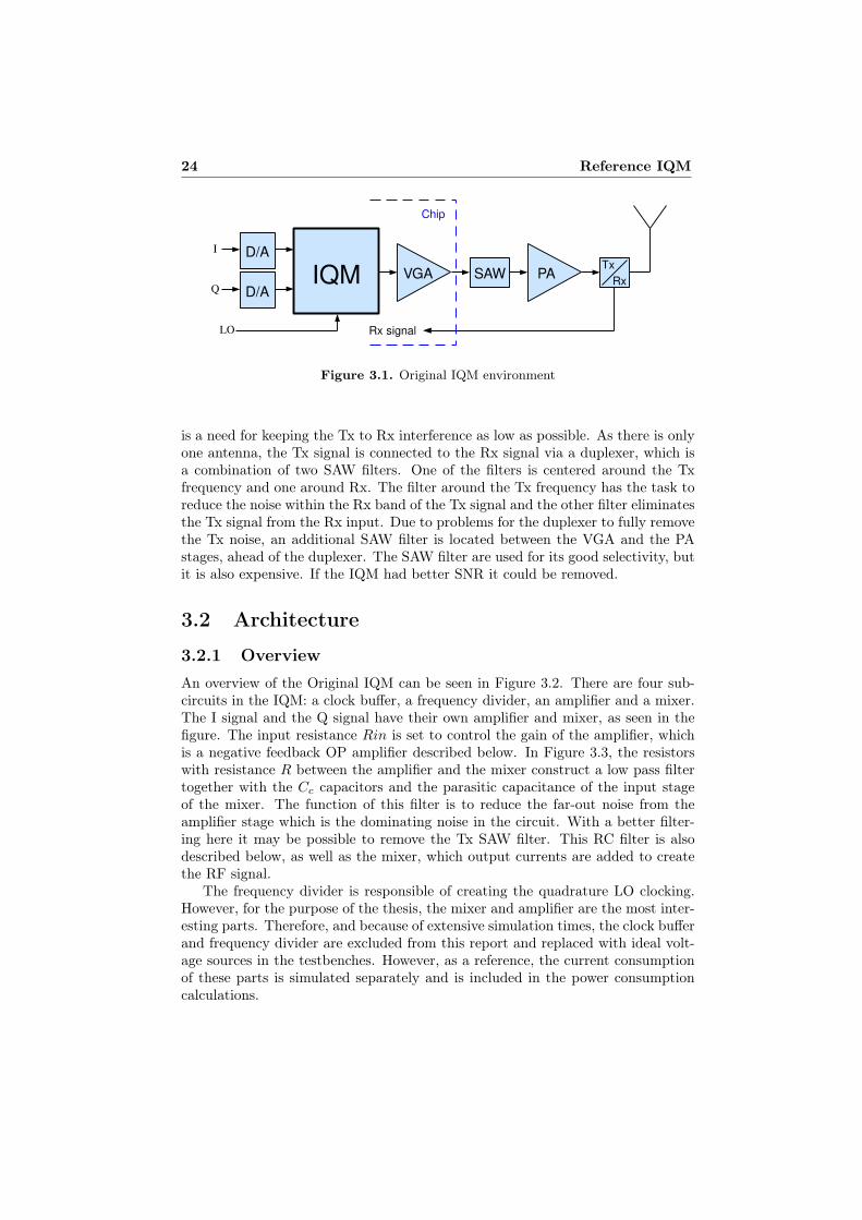
3.1 Environment
The Original IQM is embedded in the Tx part of the chip. It receives baseband Iand Q signals from the digital domain, via DA converters. After mixing the base-band signals with the LO frequency, the RF signal is put through a VGA (VariableGain Amplifier) stage. As transmitting and receiving is done simultaneously inWCDMA/LTE and the closest Rx channel is only 45 MHz higher than Tx, there
23
24 Reference IQM
Figure 3.1. Original IQM environment
is a need for keeping the Tx to Rx interference as low as possible. As there is onlyone antenna, the Tx signal is connected to the Rx signal via a duplexer, which isa combination of two SAW filters. One of the filters is centered around the Txfrequency and one around Rx. The filter around the Tx frequency has the task toreduce the noise within the Rx band of the Tx signal and the other filter eliminatesthe Tx signal from the Rx input. Due to problems for the duplexer to fully removethe Tx noise, an additional SAW filter is located between the VGA and the PAstages, ahead of the duplexer. The SAW filter are used for its good selectivity, butit is also expensive. If the IQM had better SNR it could be removed.
3.2 Architecture
3.2.1 Overview
An overview of the Original IQM can be seen in Figure 3.2. There are four sub-circuits in the IQM: a clock buffer, a frequency divider, an amplifier and a mixer.The I signal and the Q signal have their own amplifier and mixer, as seen in thefigure. The input resistance Rin is set to control the gain of the amplifier, whichis a negative feedback OP amplifier described below. In Figure 3.3, the resistorswith resistance R between the amplifier and the mixer construct a low pass filtertogether with the Cc capacitors and the parasitic capacitance of the input stageof the mixer. The function of this filter is to reduce the far-out noise from theamplifier stage which is the dominating noise in the circuit. With a better filter-ing here it may be possible to remove the Tx SAW filter. This RC filter is alsodescribed below, as well as the mixer, which output currents are added to createthe RF signal.
The frequency divider is responsible of creating the quadrature LO clocking.However, for the purpose of the thesis, the mixer and amplifier are the most inter-esting parts. Therefore, and because of extensive simulation times, the clock bufferand frequency divider are excluded from this report and replaced with ideal volt-age sources in the testbenches. However, as a reference, the current consumptionof these parts is simulated separately and is included in the power consumptioncalculations.

3.2 Architecture 25
Figure 3.2. Overview of Original IQM
Figure 3.3. Overview of Reference IQM
Name ValueRin 2 kΩR 500 ΩCc 7.73 pF
Table 3.1. Component values of Reference IQM
26 Reference IQM
3.2.2 Amplifier
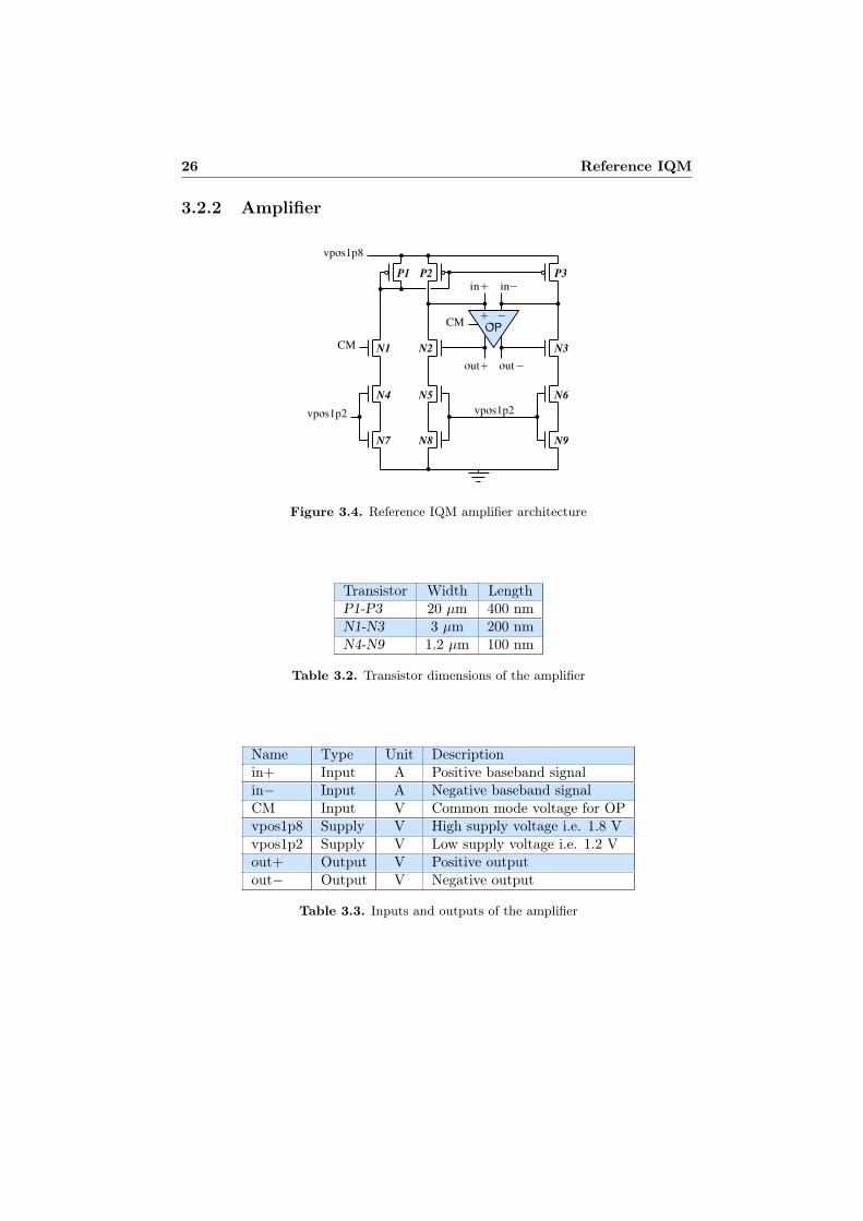
Figure 3.4. Reference IQM amplifier architecture
Transistor Width LengthP1-P3 20 µm 400 nmN1-N3 3 µm 200 nmN4-N9 1.2 µm 100 nm
Table 3.2. Transistor dimensions of the amplifier
Name Type Unit Descriptionin+ Input A Positive baseband signalin− Input A Negative baseband signalCM Input V Common mode voltage for OPvpos1p8 Supply V High supply voltage i.e. 1.8 Vvpos1p2 Supply V Low supply voltage i.e. 1.2 Vout+ Output V Positive outputout− Output V Negative output
Table 3.3. Inputs and outputs of the amplifier

3.2 Architecture 27
The amplifier circuit in Figure 3.4 is a fully differential operational amplifierwith a negative feedback over transistors N2 and N3. The feedback loop controlsthe output gain and keeps it at a wanted level. The common mode voltage for theOP is also used as a bias voltage applied at the gate of N1 creating a bias current,which is mirrored through the PMOS transistors at the top. As the transistorsin the loop are designed to match the mixer (see Figure 3.5), this mirrored biascurrent is the maximum output current in the mixer stage. The amplifier stageis also a predistortion of the signal, increasing linearity, as described in Section2.10. The OP used in the circuit is as stated an ideal component with a gain of100. The Verilog-A code of the OP is included below. With this design, a commonmode value of 960 mV gives a symmetrical input current swing through the inputresistors (Rin), which is the task for the OP common mode voltage. The commonmode of the OP has no relationship to the input common mode voltage except toget a symmetrical input current swing so that there is no DC current drawn fromthe input sources.
//Veri log−A for OP
‘ i n c lude " cons tant s . vams"‘ i n c lude " d i s c i p l i n e s . vams"
module TxLpfDiffOpamp (Outn , Outp , Cm, Gnd, Vcc , Inn , Inp ) ;output Outn , Outp ;input Inn , Inp ;inout Vcc ,Gnd,Cm;e l e c t r i c a l Outn , Outp , Inn , Inp ,Gnd, Vcc ,Cm;r e a l sp [ 0 : 1 ] ;parameter r e a l Gain = 100 ;parameter r e a l Rin = 12K;parameter r e a l Rout = 75 ;
branch ( Inp , Inn ) In ;branch (Outp , Outn) Out ;
analog beginI ( In ) <+ V( In )/Rin ;V(Out) <+ I (Out)∗Rout ;sp [ 0 ] = −1.000000∗2∗ ‘M_PI∗1G;sp [ 1 ] = 0 ;
V(Outp ,Gnd) <+ laplace_zp (V( In )∗Gain , , sp )∗0.5+V(Cm) ;V(Outn ,Gnd) <+ −1∗ laplace_zp (V( In )∗Gain , , sp )∗0.5+V(Cm) ;
endendmodule

28 Reference IQM
3.2.3 Mixer
The task for the mixer is to combine the amplified baseband signals with the LOfrequency to obtain the wanted RF signal. This is done with the quadrature LOsignals generated by the frequency divider. The frequency divider generates threedifferential signals: LO, divLOI and divLOQ. Inside the I part mixer (see Figure3.5) the positive LO signal and the divLOI signal creates two 25% duty cycle clocksfor the transistor columns, alternating between keeping column I2 and I3 activewith keeping column I1 and I4 active. In the Q mixer, with the negative part ofthe LO signal and the divLOQ signal, the opposite two 25% duty cycle clocks arecreated. This means that, in the full system, there are always one column pairactive at a time, alternating between the I part mixer and the Q part mixer. Adescription of how the duty cycles are created can be found in Figure 3.6. Theideal clock generating sources replacing the clock buffer and frequency divider areperfectly ideal with a voltage swing of 0 to 1.2 V and no rise or fall time.
Figure 3.5. Reference IQM mixer architecture (I-part)
Transistor Width LengthN1-N4 3.12 µm 250 nmN5-N8 2.32 µm 200 nmN9-N16 960 nm 100 nm
Table 3.4. Transistor dimensions of the mixer

3.2 Architecture 29
Name Type Unit DescriptionBBI+ Input V Positive amplified baseband signalBBI− Input V Negative amplified baseband signaldivLOI+ Clock V Positive In-phase frequency divided LO signaldivLOI− Clock V Negative In-phase frequency divided LO signalLO+ Clock V In-phase LO signalon Input V 1.8V ⇒ Enable, 0V ⇒ Disablevpos1p8 Supply V High supply voltage i.e. 1.8 Vvpos1p2 Supply V Low supply voltage i.e. 1.2 Viout+ Output A Positive outputiout− Output A Negative output
Table 3.5. Inputs and outputs of the I-part mixer
(a) LO signals (b) Duty cycles
Figure 3.6.
The 25% duty cycle clocking in this circuit is not a conventional mixer design, itis more common to use 50% duty cycle. In Figure 3.7, the I part of a conventionalmixer with 50% duty cycle is shown. The Q part is connected from the right inthe figure. Using this clocking, all 4 columns (I and Q) are active at all time,consuming 2 times the current as in the mixer using 25% duty cycle. However,the conventional mixer has twice the output power as well. This can be seen inthe conversion gain of the LO signals. The Fourier series of a square wave with aduty cycle of η is:
s(t) = η + 2
∞∑
n=1
sin(nπη)
nπcos(nω0t) (3.1)

30 Reference IQM
By looking at the differential clock signal, where the differential clock is sdiff (t) =s(t) − s(t + π), its Fourier series is:
s(t) =4
π
∞∑
n=0
sin([2n + 1]πη)
2n + 1cos([2n + 1]ω0t) (3.2)
At the LO frequency (n=0) a conversion gain from each clock signal is 4π at 50%
duty cycle (η = 0.5) and 4√2π
at 25% duty cycle (η = 0.25), giving half the powerof a 50% duty cycle conversion.
In the Reference IQM design though, only two of the eight columns are activeat a time, also halving the propagated noise. This means that the 25 % duty cyclemixer is consuming half the current, producing half the output power comparedto the 50 % clocking but keeping the SNR constant.
Figure 3.7. I part of conventional 50% duty cycle IQM

3.2 Architecture 31
3.2.4 RC filter
Between the amplifier and mixer, an RC-filter is located with the task to reducethe noise of the differential output from the amplifier. The resistors along withthe parasitic gate capacitances of the N5-N8 transistors in the mixer (see Figure3.5) are the components of this filter. By adding extra capacitors in parallelwith the parasitics, one can reduce the cutoff frequency of the filter and therebysuppress more noise. The total effective capacitance is represented by Ct which isthe physical capacitor combined with the parasitic capacitance. The theoreticalarchitecture of the filter can be seen in figure 3.8, where A is the differential outputfrom the amplifier, M is the input to the mixer, R is the value of the resistors andCt symbolizes the total effective capacitance as stated above.
(a) (b)
Figure 3.8. Theoretical RC filter circuits
Theoretically speaking there are 2 different filters, though with the same fre-quency response. The first one is a common mode filter that consists of 1 resistorand 1 parasitic capacitance added with the extra capacitor, represented by the redline in figure 3.8(a). There are 2 copies of this filter, one for each of the singleended signals. The filter has an RC constant according to equation 3.3 whichcomes from the serial coupled resistor and capacitance.
RCcm = RCt (3.3)
The second filter is a differential filter which consists of the 2 resistors and bothtotal capacitances. Due to the ground connection of the capacitors, they have onemutual node, which implies a serial connection of the two Ct capacitances in adifferential view. The blue line in figure 3.8(b) shows the path which creates thedifferential filter. The calculation of the RC constant for the differential filter isshown below.
RCdiff = 2RCt
2= RCt (3.4)

32 Reference IQM
As can be seen in equations 3.3 and 3.4 the RC constants is the same for thedifferential and single ended filters (RCdiff = RCcm), which results in the samecutoff frequency for both filters, described in equation 3.5.
f3dB =1
2πRCt(3.5)
The effective value of the parasitic capacitance was obtained by performing anAC analysis of the filter. With values for f3dB and R, one can easily calculateCp using equation 3.5. With R = 500 Ω, the parasitic capacitance was calculatedto Cp = 226 fF. To suppress noise but still make sure that possible 10 MHz LTEbaseband signals are forwarded, the wanted cutoff frequency was set to f3dB = 40MHz for this thesis work. The filter can be unpredictable and unstable if onlyrelying on the parasitics, therefore the added capacitors (Cc) should be larger thanCp. The above values gives a Cc of 7.73 pF which results in the total capacitanceCt = Cc + Cp = 7.96 pF. The simulated frequency response of the filter is shownin Figure 3.9. As stated in Section 1.3, all mixer components has a multiplicity of70, hence the calculated Cp symbolizes the effective gate capacitance of 70 mixerstages.
Figure 3.9. RC filter frequency response
3.3 Simulations and results 33
3.3 Simulations and results
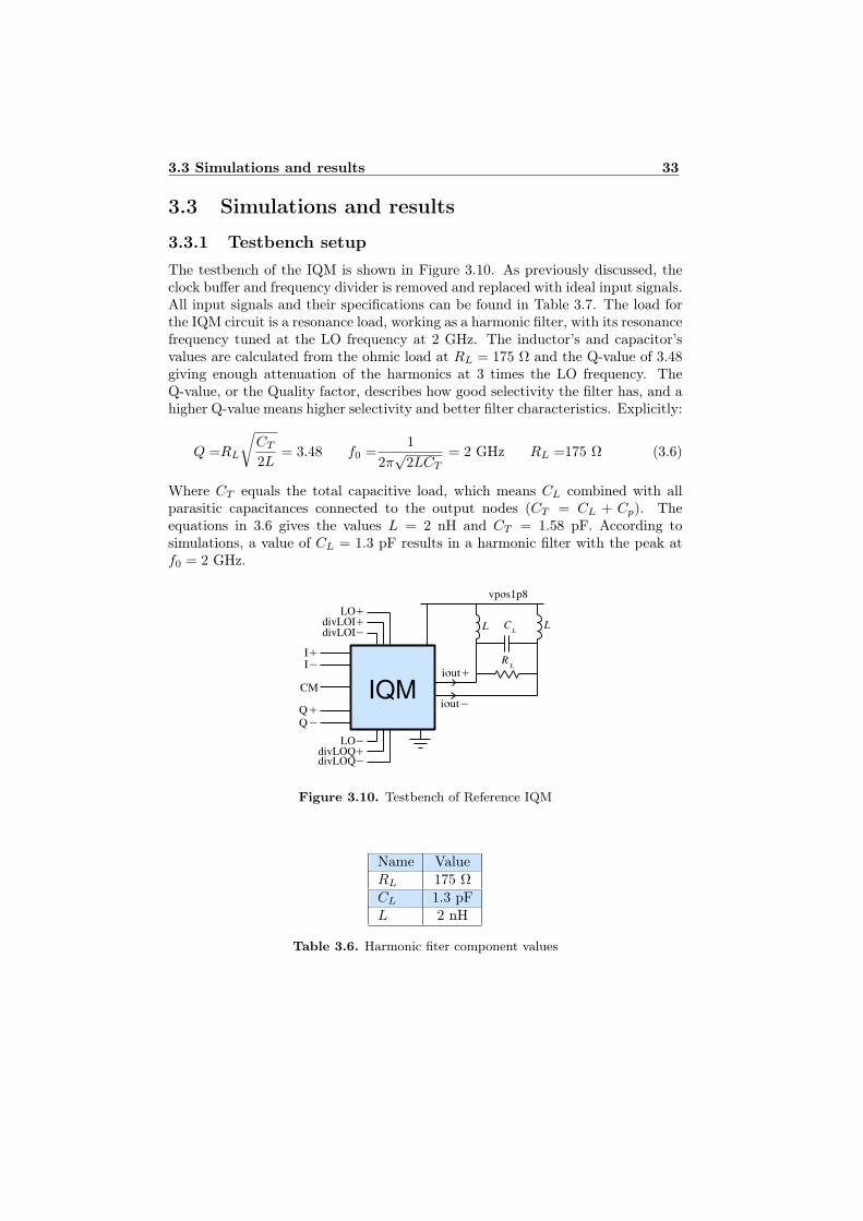
3.3.1 Testbench setup
The testbench of the IQM is shown in Figure 3.10. As previously discussed, theclock buffer and frequency divider is removed and replaced with ideal input signals.All input signals and their specifications can be found in Table 3.7. The load forthe IQM circuit is a resonance load, working as a harmonic filter, with its resonancefrequency tuned at the LO frequency at 2 GHz. The inductor’s and capacitor’svalues are calculated from the ohmic load at RL = 175 Ω and the Q-value of 3.48giving enough attenuation of the harmonics at 3 times the LO frequency. TheQ-value, or the Quality factor, describes how good selectivity the filter has, and ahigher Q-value means higher selectivity and better filter characteristics. Explicitly:
Q =RL
√
CT
2L= 3.48 f0 =
1
2π√
2LCT
= 2 GHz RL =175 Ω (3.6)
Where CT equals the total capacitive load, which means CL combined with allparasitic capacitances connected to the output nodes (CT = CL + Cp). Theequations in 3.6 gives the values L = 2 nH and CT = 1.58 pF. According tosimulations, a value of CL = 1.3 pF results in a harmonic filter with the peak atf0 = 2 GHz.
Figure 3.10. Testbench of Reference IQM
Name ValueRL 175 ΩCL 1.3 pFL 2 nH
Table 3.6. Harmonic fiter component values

34 Reference IQM
Name Type Signal level[min max]
Unit
I+ Input [600 1200] mVI− Input [600 1200] mVQ+ Input [600 1200] mVQ− Input [600 1200] mVCM Input 960 mVdivLOI+ Clock [0.0 1.2] VdivLOI− Clock [0.0 1.2] VLOI Clock [0.0 1.2] VdivLOQ+ Clock [0.0 1.2] VdivLOQ− Clock [0.0 1.2] VLOQ Clock [0.0 1.2] Vvpos1p8 Supply 1.8 Vvpos1p2 Supply 1.2 V
Table 3.7. Reference IQM testbench signals
3.3.2 Power consumption
The testbench has two voltage supplies, one at 1.2 V and one at 1.8 V, wherein this testbench the 1.2 V is used for biasing some transistors in the amplifiercircuit. The absolute majority (>99.999%) of the DC current is drawn from the1.8 V supply, which generates the current and power consumptions presented inTable 3.8. The average output power with an SSB baseband signal at 10 MHz wasin this case 5.5 dBm, giving a transmitter efficiency of 10.5 %.
Average current consumption 19.0 mAAverage power consumption 34.2 mWAverage output power 5.5 dBmTransmitter efficiency 10.5 %
Table 3.8. Results from the Reference IQM
To give a better idea of the power consumption of a complete IQM circuit,the current consumption of the LO generating circuits, i.e. the clock buffer andfrequency divider, was simulated apart from the testbench and added to the abovevalues. The resulting current and power consumption can be seen in Table 3.9,where the added overhead current consumption is 10.9 mA with a supply voltageof 1.2 V.

3.3 Simulations and results 35
Average current consumption @ 1.2 V 10.9 mAAverage current consumption @ 1.8 V 19.0 mAAverage power consumption 53.8 mWAverage output power 5.5 dBmTransmitter efficiency 7.6 %
Table 3.9. Results from the Reference IQM with added clock generation overhead
3.3.3 Linearity
The IM3 specification for the IQM is -37 dBc. However, due to the circuit mod-ifications with the ideal clocking and OP there is an improvement of linearity.
Relative IM3 distortion -43.5 dBc
Table 3.10. Result from the Reference IQM
Figure 3.11. Relative differential output power of Reference IQM

36 Reference IQM
3.3.4 Noise
The noise for the Reference IQM is presented in Figure 3.12. The relative noisespectrum density at 45 MHz offset (the nearest Rx channel) is found in the tablebelow.
The presented results does not show the real truth about the noise levels,due to the many ideal devices as the OP and clock generation. However, theyare presented here to make a comparison possible between this circuit and theEnvelope Tracking IQM.
Relative noise spectrum densityat 45 MHz offset
-169.9 dBc/Hz
Table 3.11. Noise result for the Reference IQM
Figure 3.12. Differential noise power spectrum density at output, marker at 2035 MHz

Chapter 4
Current Mode Envelope
Tracking IQM
4.1 Theory
The basic idea of this version of the IQ modulator is to make the current consump-tion of the circuit to be somewhat proportional to the input amplitude. Meaningthat while the input amplitude is high, the IQM has a high current consumption,whilst a low input results in a lower consumption. This should result in a highbenefit for signals with a high PAR value, such as LTE.
In the Reference IQM the P2 and P3 transistors of the amplifier (same as inFigure 4.3) serves as constant current sources. By substituting the common modevoltage of the OP with the envelope tracking signal (ET ), and replace the PMOStransistors with adjustable current sources which depend on the envelope of thebaseband input signal, the current consumption of the amplifier will have a relationto the amplitude of the input. The envelope signal of a sinusoidal input can beseen in Figure 4.1 and Figure 4.2 shows the theoretical layout of the modifiedamplifier circuit where the NMOS transistors are the same as in the amplifier ofthe Reference IQM.
As the current through the adjustable current sources decreases, the currentthrough the N2 and N3 transistors also has to be decreased to prevent the inputnodes from dropping in voltage. The relationship of the currents in the inputnodes is described by equation 4.1.
iN = iCS + iIN (4.1)
The amplifier will draw a current (iIN ) from the input signal when the current(iCS) through the current sources decreases, to maintain the constant commonmode current through N2 and N3 (iN ). This can cause problems for the buffersin the DACs preceding the IQ modulator if iIN becomes to great.
To prevent the voltage drop in the input node, the common mode voltage for theOP also has to follow the envelope of the input signal. This will cause the common
37

38 Current Mode Envelope Tracking IQM
Time
Am
plitu
de
(V)
envelopevinpvinn
Figure 4.1. Differential sinusoidal input signal and envelope tracking signal
Figure 4.2. Theoretical envelope tracking amplifier circuit
mode level of the OP output to decrease in proportion to the envelope signal andhence result in a lower current iN . So by varying iN and iCS in proportion tothe envelope signal, iIN can be maintained at the same level as when driving thecircuit without the envelope tracking current sources.
As the amplifier stage works as a current mirror for the mixer, the lowered biascurrent in the amplifier will also affect the mixer stage where the real benefit isachieved, because of the 70 copies of the mixer.
4.2 Implementation
The implementation of the Envelope Tracking IQM is rather simple, assumingthat all components can handle the variations of the common mode voltage for

4.2 Implementation 39
Figure 4.3. Envelope Tracking IQM amplifier architecture
the chosen baseband frequency. By replacing the constant common mode voltage(CM) for the amplifier circuit with the envelope tracking signal (ET ), there willbe a common mode mirroring of the currents through the N2 and N3 transistors,which will vary according to the amplitude of the input signal. The PMOS currentmirrors at the top of the circuit will follow the same pattern and thereby act asadjustable current sources. The envelope signal was created by implementing anFWR (Full-Wave Rectifier) which is described in Section 4.2.1.
The RC filter of the circuit was also changed due to the high frequency com-ponents of the envelope tracking signal, this is described in Section 4.2.2. Anoverview of the Envelope Tracking IQM can be seen in Figure 4.4.
Name ValueRin 2 kΩR 500 ΩCc 411 fFCd 3.66 pF
Table 4.1. Component values of Envelope Tracking IQM
4.2.1 Rectifier
The design of the rectifier is far from optimized and was mainly constructed togive a hint on how to implement an FWR as an analog circuit and to show a roughexample of the overhead current consumption of such a circuit. If implemented, itis most likely that the envelope signal will be designed as a digital signal, to give

40 Current Mode Envelope Tracking IQM
Figure 4.4. Overview of Envelope Tracking IQM
the user full control over the shape and levels of the signal. Therefore, the analogFWR will not be described in detail, only a brief description of the functionalityand the design will be presented here. The created circuit has an average currentconsumption of 705 µA and can be seen in figure 4.5.
Figure 4.5. Schematic view of the full-wave rectifier
The first block of the circuit creates a rectified shape of the input signal, referredto as the envelope signal. Block 2 subtracts the common mode voltage fromthis envelope to bring its minimum voltage level down to zero. To get a correctsubtraction, the transistor sizes of block 1 and 3 are matched. The output of block2 controls the current mirror in block 4, where the sizes of the PMOS transistorscan be changed to adjust the amplification of the output. Block 5 is designed tomatch the transistor schematic of the amplifier (see figure 4.2) and the out signal

4.2 Implementation 41
is what will be replacing the common mode voltage.
An ideal FWR was also designed, using Verilog-A code and block 5 from Figure4.5 to create a correct current mirror with the amplifier circuit. This is the FWRused for all simulations and is described by Figure 4.6. The Verilog-A block gen-erates an envelope tracking current with a fully adjustable swing with a maximumoutput of 153 µA, resulting in an output voltage of 960 mV. In the code examplebelow the envelope tracking current has a full swing of 153 µA.
Figure 4.6. Ideal full-wave rectifier
//Veri log−A for FWR
//Generates an enve lope t ra ck ing current o f the d i f f e r e n t i a l input
‘ i n c lude " d i s c i p l i n e s . vams"
module ExFWR( inp , inn , out ) ;inout inp , inn , out ;e l e c t r i c a l inp , inn , out ;r e a l vinp , vinn , i ou t ;parameter r e a l vinmax = 300m; //Maximum input ac ampl i tudeparameter r e a l voutmin = 153u ; //Maximum output currentparameter r e a l voutmin = 0 ; //Minimum output current
analog beginvinp = V( inp ) ;vinn = V( inn ) ;i ou t = ( abs ( vinp − vinn )/2)/ vinmax ; //Normalized ab so l u t e va luei ou t = −( i ou t ∗( ioutmax−ioutmin)+ioutmin ) ;
I ( out ) <+ iout ;end
endmodule

42 Current Mode Envelope Tracking IQM
4.2.2 RC filter
When implementing the envelope tracking into the circuit, a modification of theRC filter between the amplifier and mixer had to be made. The envelope signalhas a lot of high frequency components (see Figure 4.7) which are suppressed bythe present common mode filter of the Reference IQM with a cutoff frequency at40 MHz. As described in Section 3.2.4, the purpose of the RC filter is to reducethe noise of the differential signal. This means that the cutoff frequency of thedifferential filter should be kept at the same value, whilst a wider bandwidth iswanted for the common mode filter. Observing the figure, one can see that thepresented envelope signal has many high frequency components. One should beable to cut off a significant part of the highest frequencies without loosing toomuch performance. However, this thesis uses fully ideal envelope tracking.
The presented frequency spectrum is for the 10 MHz sinusoidal input usedthroughout the thesis. Though, the frequency spectrum will have different shapesfor different signals, i.e. GSM, EDGE, WCDMA and LTE.
Figure 4.7. Frequency spectrum of envelope signal for 10 MHz sinusoidal input
By inserting a capacitor between the differential inputs of the mixer, the differ-ential filter gains an extra RC component of 2RCd which can be derived from thegreen line in Figure 4.8. The resulting differential filter has the cutoff frequencypresented by equation 4.2. The cutoff frequency of the common mode filter isfound in equation 4.3 and is derived using the same relationship as in Section3.2.4 (the red line).
f3dB_diff =1
2πR(Ct + 2Cd)(4.2)

4.2 Implementation 43
f3dB_cm =1
2πRCt(4.3)
Where Ct = Cc + Cp.
Figure 4.8. Modified RC filter circuit for Envelope Tracking IQM
To widen the bandwidth of the common mode filter Ct has to be decreased.This change will also increase the differential bandwidth if Cd = 0. That is whyCd has to be increased when Ct is decreased to maintain the differential cutofffrequency. The common mode filter cutoff frequency is set to 500 MHz for theEnvelope Tracking IQM and with a maintained differential cutoff frequency of 40MHz the resulting component values are; R = 500 Ω, Cc = 411 fF, Cd = 3.66 pFand Cp still at 226 fF.
A potential problem with the different filter bandwidths, which has not beenanalyzed during this thesis work due to lack of time, is that different bandwidthsresults in different group delays. Meaning that the common mode part of the signalwill propagate faster than the differential part because of the higher common modebandwidth, causing an offset between the signal parts when arriving at the inputto the mixer. An idea to solve this problem is to insert a delay for the envelopesignal equal to the time offset of the common mode and differential signal parts.

44 Current Mode Envelope Tracking IQM
(a) Differential filter
(b) Common mode filter
Figure 4.9. Frequency response for the new RC filters
4.3 Simulations and results 45
4.3 Simulations and results
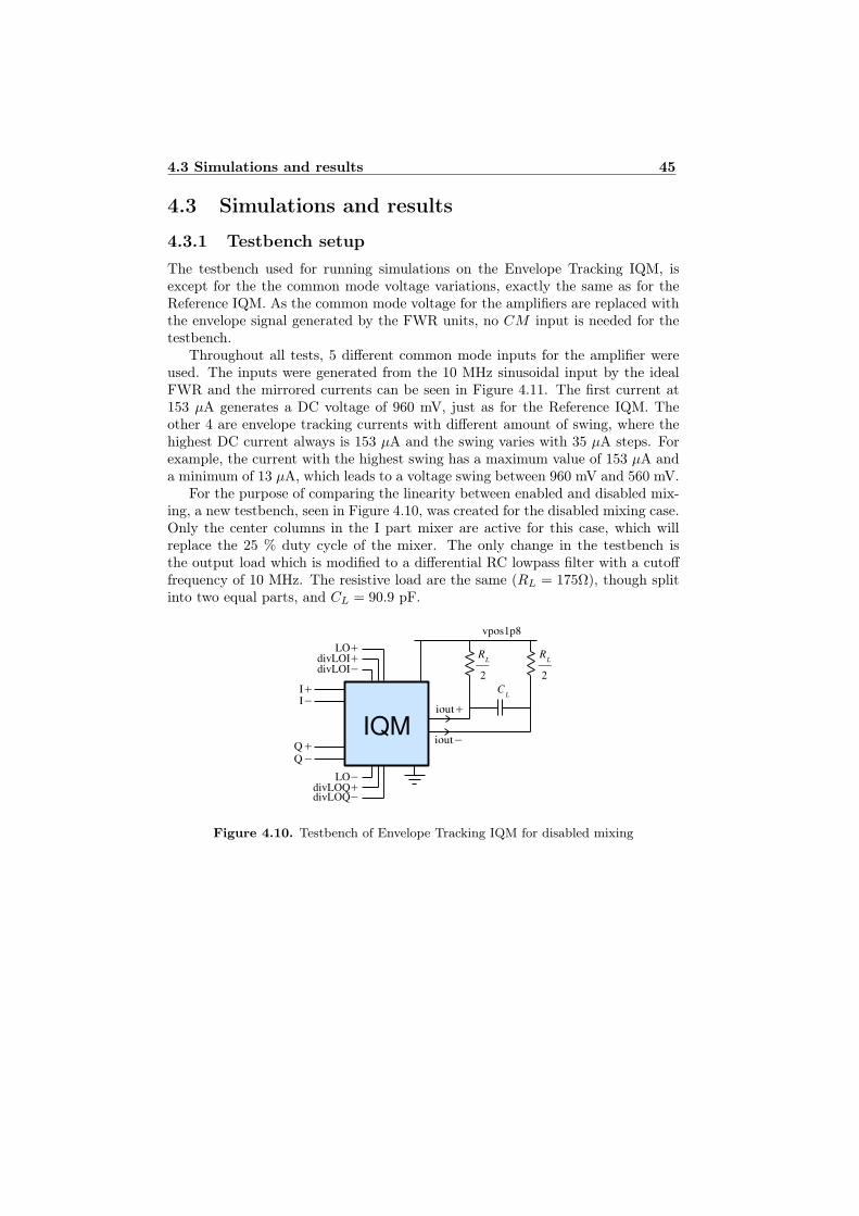
4.3.1 Testbench setup
The testbench used for running simulations on the Envelope Tracking IQM, isexcept for the the common mode voltage variations, exactly the same as for theReference IQM. As the common mode voltage for the amplifiers are replaced withthe envelope signal generated by the FWR units, no CM input is needed for thetestbench.
Throughout all tests, 5 different common mode inputs for the amplifier wereused. The inputs were generated from the 10 MHz sinusoidal input by the idealFWR and the mirrored currents can be seen in Figure 4.11. The first current at153 µA generates a DC voltage of 960 mV, just as for the Reference IQM. Theother 4 are envelope tracking currents with different amount of swing, where thehighest DC current always is 153 µA and the swing varies with 35 µA steps. Forexample, the current with the highest swing has a maximum value of 153 µA anda minimum of 13 µA, which leads to a voltage swing between 960 mV and 560 mV.
For the purpose of comparing the linearity between enabled and disabled mix-ing, a new testbench, seen in Figure 4.10, was created for the disabled mixing case.Only the center columns in the I part mixer are active for this case, which willreplace the 25 % duty cycle of the mixer. The only change in the testbench isthe output load which is modified to a differential RC lowpass filter with a cutofffrequency of 10 MHz. The resistive load are the same (RL = 175Ω), though splitinto two equal parts, and CL = 90.9 pF.
Figure 4.10. Testbench of Envelope Tracking IQM for disabled mixing

46 Current Mode Envelope Tracking IQM
Figure 4.11. Envelope signal of 10 MHz sinusoidal

4.3 Simulations and results 47
4.3.2 Power consumption
Below are two tables with the power consumption data for simulations with a 10MHz sinusoidal baseband signal, where Table 4.2 disregards the clock buffer andfrequency divider and Table 4.3 includes the current consumption of 10.9 mA with1.2 V supply for the generation of the LO signals. Five columns are present withdata for the different envelope currents described in Figure 4.1.
If having a full envelope swing of 100 %, the theoretical current consumptionfor a sinusoidal input is 2
π ≈ 64 %, which is the mean value of a rectified sine wave.The current consumption for 92 % envelope tracking is 75 % of the consumptionfor 0 % envelope tracking. So the gain is only 11 % away from the maximumtheoretical gain.
Envelope tracking (%) 0 23 46 69 92Avg. current consumption (mA) 18.3 17.2 16.0 14.9 13.7Avg. power consumption (mW) 33.0 30.9 28.8 26.7 24.7Avg. output power (dBm) 5.51 5.53 5.56 5.62 5.73Transmitter efficiency (%) 10.8 11.6 12.5 13.6 15.1
Table 4.2. Results from the Envelope Tracking IQM
Envelope tracking (%) 0 23 46 69 92Avg. current consumption @ 1.2 V (mA) 10.9 10.9 10.9 10.9 10.9Avg. current consumption @ 1.8 V (mA) 18.3 17.2 16.0 14.9 13.7Avg. power consumption (mW) 46.0 44.0 41.9 39.8 37.8Avg. output power (dBm) 5.51 5.53 5.56 5.62 5.73Transmitter efficiency (%) 7.7 8.1 8.6 9.2 9.9
Table 4.3. Results from the Envelope Tracking IQM with added clock generation over-head
With the calculated amplitude probabilities for the different wireless commu-nication standards from Section 2.6.7, one can estimate the possible decrease ofcurrent consumption when using envelope tracking in the circuit. By sweeping theinput amplitude between min and max value in a DC analysis, the current con-sumption for each discrete amplitude level is attained. If multiplying these currentconsumptions with the corresponding probability for each discrete amplitude leveland summing the products together, one gets an estimation of what the averagecurrent consumption for the analyzed communication standard will be.
The DC analysis had a step size of 1 mV and an amplitude interval of 0 - 300 mVwith the 5 different envelope signals as for the other simulations. Because of themixer functionality where only 2 columns are active simultaneously, only columnsI2 and I3 were active during the simulation to give a correct current consumptionvalue. The Q part mixer was disabled throughout the simulation. As the DC

48 Current Mode Envelope Tracking IQM
analysis does not take the mixing into concern, this gives a good estimation of thecurrent consumption as stated above. To get more exact data one should generateinput data for the different standards and run simulations with active mixing incadence. This was not done because of the longer simulation times.
Table 4.4 shows the resulting average current consumptions for GSM, EDGE,WCDMA and LTE for the different envelope signals and as for the PAR calcula-tions, 1 % of the highest amplitudes has been neglected from WCDMA and LTE.The current consumptions of the clock buffer and frequency divider are excludedfrom the presented values since they are not affected by the envelope tracking. Ascan be seen from the table, there are a high percentage of current consumption tobe saved, especially for the new LTE technology. The rightmost column representsa theoretical maximum swing from 0 to 153 µA to show the highest theoreticalreduction of the current consumption.
The highest gain for LTE is in this case a current reduction of 56 % for anenvelope swing of 140 µA (92 %) and a theoretical maximum reduction of 61 %.The last row contains the theoretical consumption for a sinusoidal input.
Envelope tracking (%) 0 23 46 69 92 100GSM (GMSK) 18.0 16.8 15.7 14.6 13.6 13.2EDGE (8-PSK) 18.0 15.9 13.8 11.6 9.55 8.79WCDMA (QPSK) 17.9 16.3 14.6 12.9 11.3 10.7LTE (64-QAM) 18.0 15.5 13.0 10.5 7.99 7.08Sine wave 18.0 16.8 15.5 14.2 13.0 12.6
Table 4.4. Average current consumptions (mA)
4.3.3 Linearity
Figure 4.13 shows a strong degradation in linearity when increasing the swing of theenvelope signal. As described before, the amplifier stage works as a predistortionfor the mixer stage, implying that the two stages has to be matched in the senseof transistor operating points. Figure 4.12 shows a simplified view of the currentmirror created by the amplifier and mixer, where transistors A1-A3 symbolizesthe amplifier stage and M1-M3 the mixer. The main difference is that transistorsM2 and M3 of the mixer stage are switching with the LO frequency while A2 andA3 are stable with a VG of 1.2 V, leading to a mismatch of the VGS voltages fortransistors A1 and M1.
With no envelope tracking, the circuit gets a sufficient linearity even thoughthere are some differences of the operating points of A1 and M1. However, whenvarying the common mode voltage the single ended outputs of the amplifier willhave a different shape, shown in Figure 4.15. As can be seen, the signal will geta lower average voltage when increasing the swing of the envelope signal. Thisresults in a low VGS of A1 and M1 for a longer period of time and a low VGS
implies a higher and more non-linear gain of the transistor. When adding the VS

4.3 Simulations and results 49
Figure 4.12. Simplified predestortion circuit of amplifier and mixer
mismatch induced by the switching of M2 and M3 to this fact, the pattern of thedecreasing linearity can be understood.
Figure 4.14 shows the linearity with disabled mixing, which shows that thematching between the amplifier and mixer is not a problem when there is noswitching of the LO input transistors in the mixer. This strengthens the theoryof the reason, described above, for the lowered linearity when having the mixerenabled.
A way to combat this problem would be to implement switching of the amplifiertransistors A2 and A3 as well. If done correctly this should make the voltagelevels of A1 to better match the voltage levels of M1 and thus give a more correctmirroring of the currents, which will improve the linearity.
The simulation result with 35 µA swing shows a deviation from the patternof degrading linearity. A resulting average common mode voltage of 931 mV isattained with this current swing. The authors believe that the A1 and M1 transis-tors enters a more linear region with the slightly lowered average common modevoltage. Studies of the transistor regions are proposed to fully understand thisdeviation. Also, simulations show that a common mode voltage for the amplifierat 910 mV gives the lowest average current through Rin, even if the 960 mVcommon mode gives equal peak values for the input current. This could also be acontributing factor for the deviation in linearity.
Envelope tracking (%) 0 23 46 69 92Enabled mixing -41.9 -45.6 -32.9 -26.1 -21.6Disabled mixing -41.6 -39.2 -37.9 -37.9 -40.4
Table 4.5. Relative IM3 distortion (dBc) on the Envelope Tracking IQM

50 Current Mode Envelope Tracking IQM
Figure 4.13. Relative differential output power of Envelope Tracking IQM
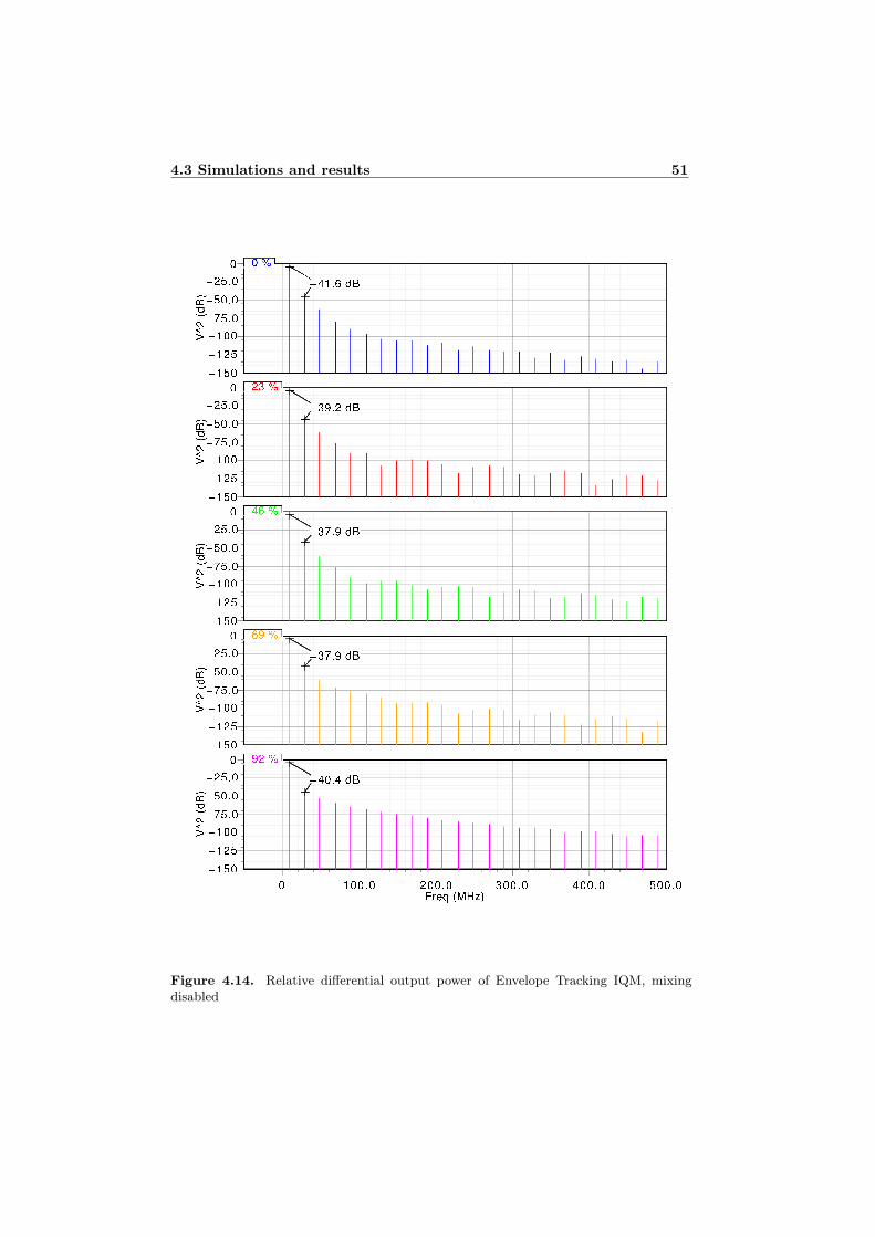
4.3 Simulations and results 51
Figure 4.14. Relative differential output power of Envelope Tracking IQM, mixingdisabled

52 Current Mode Envelope Tracking IQM
Figure 4.15. Single ended output from amplifier

4.3 Simulations and results 53
4.3.4 Noise
As can be seen in Table 4.6 and Figure 4.16, the relative noise spectrum densityat 45 MHz offset is improved with a higher swing for the envelope signal. This isdue to the increase of output power (see Table 4.2). A higher output power resultsin a higher SNR.
The values presented here are as for the Reference IQM not fully reliable be-cause of the ideal devices in the circuit, such as the OP, FWR and clock generation.
Envelope tracking (%) 0 23 46 69 92Relative noise spectrum densityat 45 MHz offset (dBc/Hz)
-169.9 -170.1 -170.2 -170.2 -170.4
Table 4.6. Noise results for the Envelope Tracking IQM

54 Current Mode Envelope Tracking IQM
Figure 4.16. Differential noise spectrum density at output, marker at 2035 MHz
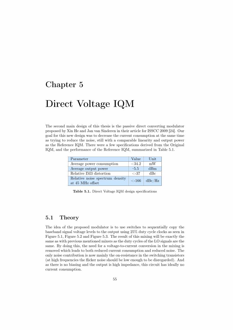
Chapter 5
Direct Voltage IQM
The second main design of this thesis is the passive direct converting modulatorproposed by Xin He and Jan van Sinderen in their article for ISSCC 2009 [24]. Ourgoal for this new design was to decrease the current consumption at the same timeas trying to reduce the noise, still with a comparable linearity and output poweras the Reference IQM. There were a few specifications derived from the OriginalIQM, and the performance of the Reference IQM, summarized in Table 5.1.
Parameter Value UnitAverage power consumption <34.2 mWAverage output power e5.5 dBmRelative IM3 distortion <-37 dBcRelative noise spectrum densityat 45 MHz offset
<-166 dBc/Hz
Table 5.1. Direct Voltage IQM design specifications
5.1 Theory
The idea of the proposed modulator is to use switches to sequentially copy thebaseband signal voltage levels to the output using 25% duty cycle clocks as seen inFigure 5.1, Figure 5.2 and Figure 5.3. The result of this mixing will be exactly thesame as with previous mentioned mixers as the duty cycles of the LO signals are thesame. By doing this, the need for a voltage-to-current conversion in the mixing isremoved which leads to both reduced current consumption and reduced noise. Theonly noise contribution is now mainly the on-resistance in the switching transistors(at high frequencies the flicker noise should be low enough to be disregarded). Andas there is no biasing and the output is high impedance, this circuit has ideally nocurrent consumption.
55
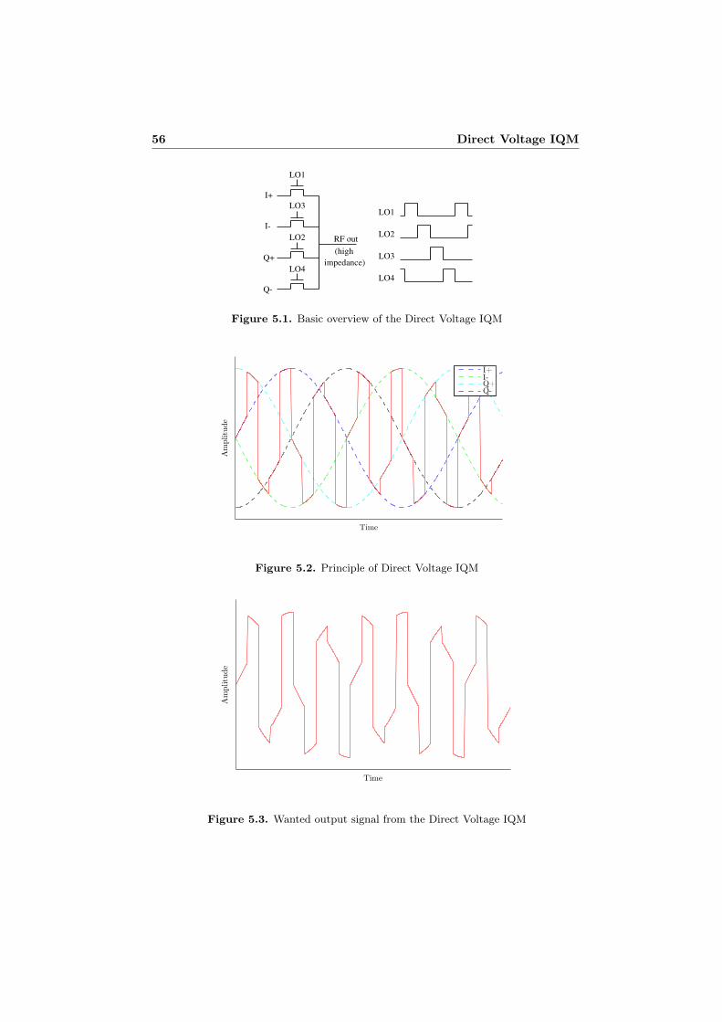
56 Direct Voltage IQM
Figure 5.1. Basic overview of the Direct Voltage IQM
Am
plit
ude
Time
I+I-Q+Q-
Figure 5.2. Principle of Direct Voltage IQM
Am
plit
ude
Time
Figure 5.3. Wanted output signal from the Direct Voltage IQM

5.1 Theory 57
Figure 5.4. Direct Voltage IQM with cascade output stage
Figure 5.5. 25% duty cycle clock
As the IQM output is connected to a VGA and to avoid driving too much fromthe DA converter in the previous circuit stage as well as to be able to keep thevariable gain property the proposed solution includes an output cascade amplifierdriver stage. This addition can be seen in the more detailed Figure 5.4. As seen,there is also a harmonic filter in the driver stage. This filter is tuned to the wantedoutput frequency, reducing the amplitudes of the harmonics.
The circuit is also designed with a first order low pass filter that filters theincoming signal to reduce the high frequency noise. This filter also absorbs thecurrent spikes from the LO signal and is thus reducing the LO leakage. As pre-viously mentioned, the highest signal bandwidth for this thesis is the LTE signalwith its 10 MHz maximum baseband signal frequency so the same cutoff frequencyas earlier is used: f3dB = 40 MHz.
Another difference from a conventional IQM is the slight alternation of the LOclock signals. As seen with ordinary clocking in Figure 5.5 a) the mixer might,during a short time, have two switches partly open at the same time. This createsan unwanted current flow from the input signal with the higher potential to theone with the lower. To reduce this effect the authors proposed the use of non-overlapping clocking, seen in Figure 5.5 b). This improves linearity and is simplyachieved by sizing the PMOS and NMOS in an LO input buffer. [24]

58 Direct Voltage IQM
Figure 5.6. Small signal noise analysis of Direct Voltage IQM
5.2 Implementation
The IQM is divided into two parts, the mixer and the output stage. To dimensionthe mixer we first needed to examine its load, the output stage. Therefore thedesign process was separated into two parts, first sizing the output stage to acquirea good SNR and then size the mixer stage once we knew the size of the load.
5.2.1 Output stage noise analysis
A small signal noise model of a differential output stage was constructed usingthe MOSFET noise model from Section 2.8.3. The importance here was to findout how the SNR in the circuit was affected by design parameters as bias currentand transistor dimensions. As the wanted frequency is high, the flicker noise wasdisregarded. First, the output signal Iout was derived from V in in Figure 5.6 a):
V in − V gs1 + V gs2 = 0gmV gs1 + gmV gs2 = 0
⇒ V gs1 = −V gs2 = V in2
Iout = gmV in2
(5.1)
To calculate the noise generated from the bottom pair of transistors, we appliedthe noise source for one transistor and calculated its influence on Iout. See Figure5.6 b).
V gs1 = V gs20gmV gs1 + id1 + gmV gs2 = 0V gs2
⇒ V gs1 =id1
2gm(5.2)
Iout = −gmV gs2 = − id1
2(5.3)

5.2 Implementation 59
This noise is also contributed from the right transistor, giving the total noisepower:
Iout2tot,noise =i2d1
4+
i2d2
4(5.4)
Finally, the noise from the cascade transistors is calculated in Figure 5.6 c) tohave no affect on the output noise as it will only be propagated to the gate of thetransistor as:
V gs1 = V gs20gmV gs1 + gmV gs2 = 0V gs2
⇒ Iout = 0V gs3 = − id3
gm
(5.5)
So, to calculate the maximum SNR in the output stage, the maximum averageoutput signal power is divided by the noise power:
SNRmax =
(
Iout√
2
)2
i2d1 + i2d2
4
=I2DC
2(i2d1 + i2d2)=
I2DC
8kBT 23gm
=3I2
DC
16kBT√
K WL IDC
(5.6)
Which means that the maximum SNR is proportional to IDC to the power of 32
and
√
L
Wof the lower transistors.
To be able to reach the goal of -166 dBc/Hz in noise spectral density for theentire IQM we decided to size the output stage at -170 dBc/Hz, using an inputvoltage swing of 600 mV.
5.2.2 Mixer dimensioning
Unfortunately, we couldn’t achieve good linearity results of the mixing with thebaseband voltage swing at 600 mV. We believe that the main reason for this wasthat the minimum VGS of the switching transistors was too low. This meansthat the on-resistance was too high and the output node didn’t finish charging ata clock frequency of 2 GHz. The baseband voltage was thus decided to have avoltage swing of 400 mV, at a DC level of 700 mV. This has a negative effect onthe SNR, as the output stage was designed to have a larger input amplitude butit had to be done to create a more linear solution.
The LO clocks could be driven to a maximum of Vdd = 1.8 V, meaning that theVGS of the switching transistors now varied from 0.9 V to 1.30 V when conducting,keeping it above threshold voltage at all times but never exceeding the oxidebreakdown voltage at 1.32 V. That also meant that there was a good DC levelfor the signal at the output stage, keeping M9 and M10 saturated. Furthermore,wide switching transistors at 40 µm were used to reduce the RC time delay of thesignal path and to decrease noise from the on-resistance.
To give a comparison on the needed size of the clock driving, we can comparethe transistor widths to the Reference IQM. Looking at a 2 GHz clock signal there,LO+ for example, its drives a total transistor width of 70x4x0.96 µm=268.8 µm,

60 Direct Voltage IQM
Figure 5.7. Schematic of the implemented Direct Voltage IQM
Transistor Width LengthM1-M8 40 µm 100 nmM9-M10 2.6 µm 200 nmM11-M12 5.2 µm 200 nm
Table 5.2. Transistor dimensions for theDirect Voltage IQM
Parameter Value UnitR 50 ΩC 79.6 pF
RBIAS 100 Ω
Table 5.3. Component values for DirectVoltage IQM
compared to only 2x40=80 µm here. Both design’s transistors have a length of100 nm.
As mentioned in Section 1.3 we are not looking at the case with variable gain,and here the output stage is implemented in 70 instances giving full gain. Thefully implemented circuit can bee seen in Figure 5.7, transistor sizes in Table 5.2and other device parameters in Table 5.3.
5.3 Simulations and results
5.3.1 Testbench setup
The Direct Voltage IQM was tested using ideal voltage sources as input signals.The 25% duty cycle clocks were generated both by a frequency divider providedfrom ST-Ericsson, here called the 4PGFD (4 Phase Generating Frequency Divider)unit, as well as using ideal voltage sources. The voltage swing from the 4PGFDcircuit was 1.2 V, therefore this clock swing was also used with the ideal clocks,with a maximum voltage of Vdd=1.8 V. The simulation time with the 4PGFD

5.3 Simulations and results 61
Figure 5.8. Direct Voltage IQM testbench
clock increased substantially so because of efficiency and also because the previousIQM:s didn’t use clock dividers or clock buffers and to compare with them, theresults below are when using an ideal clocking. Results from simulations with the4PGFD clock are included in Section 5.3.6. The non-overlapping clocking was notused in simulations as the performance was not improved, see results in Section5.3.5.
Not the same harmonic load was used in this testbench as in the previous. Thiswas due to a miscalculation in the early stages of development, not discovereduntil the end of the research. The modifications were minimum however. Thesame resistive load of 175 Ω was used but the capacitor had a capacitance of 0.63pF and the two inductors had the inductance 4.5 nH each. This gave the sameresonance frequency but with a decrease of the Q value. The new Q value was(ignoring parasitics):
Q = RL
√
CL
2L= 1.47 (5.7)
This means that, at 2 GHz resonance frequency, the filter bandwidth was increasedfrom 570 MHz to 1360 MHz. The effect of this is small and can be disregarded,as the important signals were all well inside of the 570 MHz bandwidth.
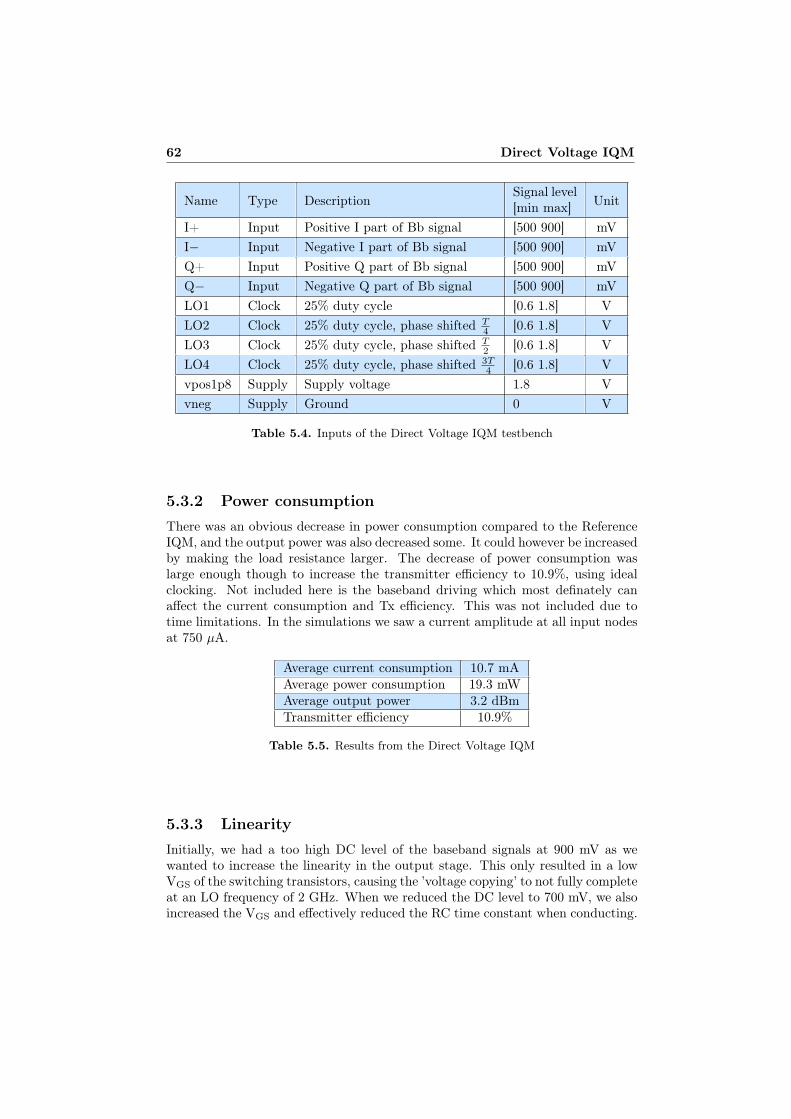
62 Direct Voltage IQM
Name Type DescriptionSignal level[min max] Unit
I+ Input Positive I part of Bb signal [500 900] mV
I− Input Negative I part of Bb signal [500 900] mV
Q+ Input Positive Q part of Bb signal [500 900] mV
Q− Input Negative Q part of Bb signal [500 900] mV
LO1 Clock 25% duty cycle [0.6 1.8] V
LO2 Clock 25% duty cycle, phase shifted T4 [0.6 1.8] V
LO3 Clock 25% duty cycle, phase shifted T2 [0.6 1.8] V
LO4 Clock 25% duty cycle, phase shifted 3T4 [0.6 1.8] V
vpos1p8 Supply Supply voltage 1.8 V
vneg Supply Ground 0 V
Table 5.4. Inputs of the Direct Voltage IQM testbench
5.3.2 Power consumption
There was an obvious decrease in power consumption compared to the ReferenceIQM, and the output power was also decreased some. It could however be increasedby making the load resistance larger. The decrease of power consumption waslarge enough though to increase the transmitter efficiency to 10.9%, using idealclocking. Not included here is the baseband driving which most definately canaffect the current consumption and Tx efficiency. This was not included due totime limitations. In the simulations we saw a current amplitude at all input nodesat 750 µA.
Average current consumption 10.7 mAAverage power consumption 19.3 mWAverage output power 3.2 dBmTransmitter efficiency 10.9%
Table 5.5. Results from the Direct Voltage IQM
5.3.3 Linearity
Initially, we had a too high DC level of the baseband signals at 900 mV as wewanted to increase the linearity in the output stage. This only resulted in a lowVGS of the switching transistors, causing the ’voltage copying’ to not fully completeat an LO frequency of 2 GHz. When we reduced the DC level to 700 mV, we alsoincreased the VGS and effectively reduced the RC time constant when conducting.

5.3 Simulations and results 63
Once this was discovered, it was possible to reach the goal at -37 dBc for the IM3.
Relative IM3 distortion -37.03 dBc
Table 5.6. Result from the Direct Voltage IQM
Figure 5.9. Relative differential output power of the Direct Voltage IQM
5.3.4 Noise
The goal at 166 dBc/Hz at 45 MHz offset was not reached, not even with theideal clocking that was used. It was very close though as seen below. To beable to reach this goal, the output stage could be redesigned, optimized with ainput signal swing at 400 mV. Also, the noise contribution from the switchingtransistors could be reduced. As this noise is amplified in the output stage andit now represents almost a third of the noise, reducing this noise could also be away to improve the performance. The noise can then be reduced by having largerswitching transistors, decreasing on-resistance and thus thermal noise.
Relative noise spectrum densityat 45 MHz offset
-165.9 dBc/Hz
Table 5.7. Noise results for the Direct Voltage IQM.

64 Direct Voltage IQM
Figure 5.10. Differential noise spectrum density, marker at 2035 MHz
Device Param Noise Contr ibut ion % Of Total
Output stage , N9 id 2.72839 e−18 29 .03Output stage , N10 id 2.72838 e−18 29 .03Mixer , N1 id 3 .575 e−19 3 .80Mixer , N2 id 3.57499 e−19 3 .80Mixer , N3 id 3.57496 e−19 3 .80Mixer , N4 id 3.57493 e−19 3 .80Mixer , N5 id 3 .5749 e−19 3 .80Mixer , N6 id 3.57486 e−19 3 .80Mixer , N7 id 3.57484 e−19 3 .80Mixer , N8 id 3.57477 e−19 3 .80Output stage , N9 fn 1.93887 e−19 2 .06Output stage , N10 fn 1.93886 e−19 2 .06Output stage , Rbias (1 ) rn 1.75117 e−19 1 .86Output stage , Rbias (2 ) rn 1.75116 e−19 1 .86Output stage , N11 id 9.46194 e−20 1 .01Output stage , N12 id 9.46193 e−20 1 .01Output stage , N9 rgb i 1 .67661 e−20 0 .18
Spot Noise Summary ( in V^2/Hz) at 2 .035GHz Sorted By Noise Contr ibutorTotal Summarized Noise = 9.39826 e−18Total Input Refer red Noise = 1.79769 e+308The above no i s e summary i n f o i s f o r pno i se data
5.3.5 Non-overlapping clock signals
We also simulated the difference in clocking as the authors to [24] proposed a non-overlapping 25% duty cycle clocking. This was achieved by slightly changing the

5.3 Simulations and results 65
ideal clocking circuit as in Figure 5.5. The results are found in Table 5.8. However,the expected results were not shown. There was actually a decrease in linearity.
Parameter Overlapping Non-overlapping UnitAverage current consumption 10.7 10.6 mAAverage power consumption 19.3 19.1 mWAverage output power 3.2 3.1 dBmTransmitter efficiency 10.9 10.7 %Relative 3rd order distortion -37.0 -36.5 dBcRelative noise spectrum densityat 45 MHz offset
-165.9 -165.8 dBc/Hz
Table 5.8. Results from simulation with and without non-overlapping clocking
We believe that the reduction in linearity comes from that the time to charge(or discharge) the output node to the baseband voltages was reduced with thenon-overlapping clocking, as the switching transistors were not open as long timeas with the overlapping clocks. This means that the ’voltage copying’ was notcomplete at 2 GHz.

66 Direct Voltage IQM
5.3.6 Simulating with 4PGFD clocking circuit
The 4PGFD circuit was designed for a 1.2 V supply voltage, so the four generatedclocks had to be AC coupled and biased to reach a maximum of 1.8 V. This wasdone using ideal DC voltage sources, increasing the DC level by 0.6 V. This resultedin a clocking voltage from 0.6 V to 1.8 V. More realistically it would be better todo this using a capacitor for AC coupling and then some biasing resistors, whichunfortunately was not done in this case due to time limitations. However, thisclocking circuit was not built especially for this IQM so it should be thought ofas more of a possible contributor to current consumption and signal degradation.With a case specific clocking, the current consumption and noise could be lowerthan this. Worth thinking of is that the clocks only need to drive two transistorseach, not as in the previous cases, 280 different transistors. This should make itpossible to design a small and efficient clocking circuit.
Parameter Ideal clocking 4PGFDclocking
Unit
Average current consumption @1.2 V
0.0 11.3 mA
Average current consumption @1.8 V
10.7 10.6 mA
Average power consumption 19.3 32.7 mWAverage output power 3.2 3.1 dBmTransmitter efficiency 10.9 6.2 %Relative 3rd order distortion -37.0 -35.1 dBcRelative noise spectrum densityat 45 MHz offset
-165.9 -165.2 dBc/Hz
Table 5.9. Results from simulations with the 4PGFD clocking circuit

5.3 Simulations and results 67
Figure 5.11. Copying of the baseband signals
Figure 5.12. Zoom of copying of the baseband signals
5.3.7 Discussion
The results of the simulations obviously showed that the new mixer design workedand there is an expected power consumption decrease. As a visual proof, thecopying of the voltage levels can be seen in Figure 5.11, to be compared with thefigure in the theory section, Figure 5.2. A zoom of the signal copying can alsobe seen in Figure 5.12. In this figure, the important occasion when VGS of theswitching transistors is at its minimum can be observed in the topmost signal. Asseen, the voltage level of that signal is successfully transferred.
Even though we met the design specifications for linearity, we noticed thatit was hard to reach the goal. A part of the problem was assumed to be withthe non-linearities in the output stage. To compensate for this, the same type ofpredistortion as in the Reference IQM was inserted, see Chapter 6.


Chapter 6
Predistorted Direct Voltage
IQM
The reason for investigating the predistorted direct voltage IQM was to increase thelinearity in such a big degree so that the Direct Voltage IQM could be designed withmuch lesser linearity constrains, giving the circuit even less current consumption.
6.1 Theory
The predistortion here is a matched current mirror, with exactly the same functionsas in the Reference IQM, as explained in Section 2.10. Here, the output cascadeamplifier driver stage of the Direct Voltage IQM is matched with a predistortioncircuit before the the actual mixing, predistorting the input signals, see Figure 6.1.As seen, there must be a transconductance stage in the predistortion as the inputvoltages needs to be converted to currents.
Figure 6.1. Predistortion of the input signals
69

70 Predistorted Direct Voltage IQM
Figure 6.2. Implementation of the Predistorted Direct Voltage IQM
Transistor Width LengthM1-M8 40 µm 100 nmM9-M10 2.6 µm 200 nmM11-M12 5.2 µm 200 nmM13-M16 2.6 µm 200 nm
Table 6.1. Transistor dimensions for thePredistorted Direct Voltage IQM
Parameter Value UnitR 50 ΩC 79.6 pF
RBIAS 100 ΩRVGA 100 Ω
Table 6.2. Component values for the Pre-distorted Direct Voltage IQM
6.2 Implementation
As the predistortion improves the linearity of the circuit and the Direct VoltageIQM already achieved the goals for linearity, there should be the possibility todecrease the baseband signal’s DC level and increase the AC amplitude givingdecreased current consumption and higher SNR on the account of the linearitygain.
It turned out that implementing this predistortion was a more demanding taskthan we first presumed. When we tested the early designs it showed that wecouldn’t achieve the linearity gain we hoped for. Initially we thought that we hadproblems with matching the predistortion to the output stage, especially as wedidn’t have the same matching network as in the Reference IQM. Instead we hadan ideal gm stage feeding the input current. So a lot of time was spent on biasingand sizing the predistortion, as well as the output stage, for a better matching.However, it was seen that we were limited by some other problem, presumably themixer. Again, the voltage levels through the switching mixers came into focus.With an increased voltage swing of the baseband signal, the minimum VGS of theswitching transistors was lower than before, we observed VGS at the size of 700-

6.3 Simulations and results 71
800 mV. This could be a reason for not attaining the wanted linearity gain. Asproblems with linearity was observed also without predistortion there can also besome other fundamental limitation of the mixer that we are not aware of. Whenwe simulated without an applied mixing, there was a linearity improvement ofroughly 5 dB in the third order distortion, again pointing at problems with themixer. Unfortunately we didn’t have the time to investigate this problem in depthand we had to settle for what performance we had. To be able to reach the linearitydemands, we actually had to decrease the input amplitude and increase the DClevel, opposite of the wanted. The baseband voltages were thus set at 50 to 850mV, converted to an input current of 12.5 µA to 212.5 µA, using a gm stage of250 µS. The transistor widths and the bias resistors were the same sizes as in theDirect Voltage IQM case.
The transconductance stages used in the implementation were ideal gm stagesas there were shortage of time to implement a well working circuit. However, themain focus with this IQ modulator was to verify the functionality of predistortingthe baseband signal to improve linearity in the RF signal, not to fully implementit in a circuit.
Also, as the input signal now was driven through a transistor, a voltage bufferhad to be inserted after the predistortion to be able to drive the output stage. Thenecessary driving at the in ports without this buffer was not investigated.
6.3 Simulations and results
6.3.1 Testbench setup
The testbench was setup in the same manner as in the Direct Voltage IQM casewith ideal overlapping clocking and the same harmonic load. For reference, the4PGFD clock circuit was also used in simulations. The input signals had differentsignal values as seen in the table below. The transconductance of the gm stage wasas earlier said set to 250 µS. The voltage buffer stages were ideal voltage-to-voltageconverters with a ratio of 1.
Figure 6.3. Predistorted Direct Voltage IQM testbench

72 Predistorted Direct Voltage IQM
Name Type DescriptionSignal level[min max] Unit
I+ Input Positive I part of Bb signal [50 850] mV
I− Input Negative I part of Bb signal [50 850] mV
Q+ Input Positive Q part of Bb signal [50 850] mV
Q− Input Negative Q part of Bb signal [50 850] mV
LO1 Clock 25% duty cycle [0.6 1.8] V
LO2 Clock 25% duty cycle, phase shifted T4 [0.6 1.8] V
LO3 Clock 25% duty cycle, phase shifted T2 [0.6 1.8] V
LO4 Clock 25% duty cycle, phase shifted 3T4 [0.6 1.8] V
vpos1p8 Supply Supply voltage 1.8 V
vneg Supply Ground 0 V
Table 6.3. Inputs of the Predistorted Direct Voltage IQM testbench
6.3.2 Power consumption
As we had troubles reaching the expected linearity gain there were not the per-formance improvements we had hoped for. To be able to reach the linearity goals,the baseband voltage swing was decreased and to achieve similar output power thebias currents were increased.
Average current consumption 16.7 mAAverage power consumption 30.1 mWAverage output power 4.1 dBmTransmitter efficiency 8.5%
Table 6.4. Results from the Predistorted Direct Voltage IQM
6.3.3 Linearity
Here is where we should see the biggest winnings compared to the non-predistortedDirect Voltage IQM. However this was not the case and to achieve a better resultoverall for this circuit, the linearity of the mixer should be examined further. Thegoal at -37 dBc for IM3 was reached however, as described in the implementationsection.
Relative IM3 distortion -38.8 dBc
Table 6.5. Result from the Predistorted Direct Voltage IQM

6.3 Simulations and results 73
Figure 6.4. Relative differential output power of Predistorted Direct Voltage IQM
6.3.4 Noise
Also the noise performance was decreased when using the predistortion. This camefrom the increased bias current in the output stage as well as the higher basebandvoltage level, increasing the on-resistance for the switching transistors.
Relative noise spectrum densityat 45 MHz offset
-165.2 dBc/Hz
Table 6.6. Noise results for the Predistorted Direct Voltage IQM

74 Predistorted Direct Voltage IQM
Figure 6.5. Noise density for Predistorted Direct Voltage IQM
Device Param Noise Contr ibut ion % Of Total
Output stage , N9 id 3.67754 e−18 27 .13Output stage , N10 id 3.67753 e−18 27 .13Mixer , N1 id 5.80915 e−19 4 .29Mixer , N2 id 5.80896 e−19 4 .29Mixer , N3 id 5 .8089 e−19 4 .29Mixer , N4 id 5.80889 e−19 4 .29Mixer , N5 id 5.80881 e−19 4 .29Mixer , N6 id 5.80875 e−19 4 .29Mixer , N7 id 5 .8086 e−19 4 .29Mixer , N8 id 5.80857 e−19 4 .29Output stage , N9 fn 2.93517 e−19 2 .17Output stage , N10 fn 2.93516 e−19 2 .17Output stage , Rbias (1 ) rn 2.58118 e−19 1 .90Output stage , Rbias (2 ) rn 2.58117 e−19 1 .90Output stage , N11 id 8.32595 e−20 0 .61
Spot Noise Summary ( in V^2/Hz) at 2 .035GHz Sorted By Noise Contr ibutorTotal Summarized Noise = 1.35528 e−17Total Input Refer red Noise = 1.79769 e+308The above no i s e summary i n f o i s f o r pno i se data

6.3 Simulations and results 75
6.3.5 Simulating with 4PGFD clocking circuit
Also here simulations with the 4PGFD were made. Keep in mind though, asstated in Section 5.3.6, that this clocking circuit is not optimized for this IQMand the results are here to give a hint about total current consumption and signaldegradation.
Parameter Ideal clocking 4PGFDclocking
Unit
Average current consumption @1.2 V
0.0 11.3 mA
Average current consumption @1.8 V
16.7 16.6 mA
Average power consumption 30.1 43.3 mWAverage output power 4.1 4.0 dBmTransmitter efficiency 8.5 5.8 %Relative 3rd order distortion -38.8 -37.0 dBcRelative noise spectrum densityat 45 MHz offset
-165.2 -164.6 dBc/Hz
Table 6.7. Results from simulations with the 4PGFD clocking circuit


Chapter 7
Conclusions
The work of this thesis showed that there is a great potential for both types of IQmodulators, envelope tracking and direct converting, to reduce the current con-sumption of the IQ modulator circuit. There is however no clear winner becauseof the ideal devices used for some of the designs. Using the amplitude analysisof the different communication standards when calculating the reduction of cur-rent consumption in the Current Mode Envelope Tracking, very good results wereachieved. For example, with the LTE signals having an I/Q PAR0.99 of 8.4 dB, thecurrent consumption was decreased with as much as 56 %, or 10 mA, for the casewith 92 % envelope tracking according to calculations, though with the cost ofdecreased linearity. Even if it might be very hard to construct such high envelopetracking within the linearity requirements, using a moderate tracking with only 23% swing still reduced the current consumption by 2.5 mA. The major obstacle inthe way of these current consumption reductions are the matching of the amplifierand the mixer stages, which reduces the linearity when increasing the envelopetracking.
With the Direct Voltage IQM, it could be seen that as long as the switching ofthe signals was done satisfactory, a reduction in current consumption was achieved.Having an output power of 4.0 dBm, the IQM had a power consumption of 43.3mW, including the clocking circuits. If also the noise of the switching transistorswas reduced some, this circuit could even be designed to match the noise criteriafor a SAW-less design, reducing cost and area. However, one big question markremains and that is from Chapter 6, the unsuccessful predistortion of the DirectVoltage IQM. The theories of why we cannot achieve the expected linearity im-provements are mostly pointing at the mixer. Spending more time investigatingthese non-linearities would probably result in a performance increase.
77

78 Conclusions
IQM designAveragepowerconsumption
Averageoutputpower
Txefficiency
IM3
Reference 34.2 mW 5.5 dBm 10.5 % -43.5 dBcEnvelopeTracking 23 %
30.9 mW 5.5 dBm 11.6 % -45.6 dBc
EnvelopeTracking 92 %
24.7 mW 5.7 dBm 15.1 % -21.6 dBc
Direct Voltage 19.3 mW 3.2 dBm 10.9 % -37.0 dBcPredistortedDirect Voltage
30.1 mW 4.1 dBm 8.5 % -38.8 dBc
Table 7.1. Summary of the simulation results (clocking circuits excluded)
When considering the values in the table, one has to take into account that thethesis has not produced complete circuits to fully replace the present IQM. In thecase of the Envelope Tracking IQM, this means that with some improvements onthe amplifier circuit and the matching with the mixer, the linearity of this designshould reach the specified requirement of -37 dBc. And for the Predistorted DirectVoltage IQM, solving the linearity problems would most definitely make it ableto also decrease the current consumption by lessen the design requirements of theoutput stage.
7.1 Future work
Below follows two sections discussing proposed future work for the Envelope Track-ing IQM and the two Direct Converting versions respectively. The items are listedin descending priority, with what the authors think has the highest priority at thetop.
7.1.1 Envelope Tracking IQM
Matching amplifier and mixer
The mismatch of the transistor voltages between the amplifier output and themixer input has an increasing effect on the linearity when increasing the swing ofthe envelope signal. Shortly described the problem occurs because of the largerand more non-linear gain when VGS is small. The voltage variations due to theswitching in the mixer will then have a larger effect and thus degrading the lin-earity. The phenomenon is described in detail in Section 4.3.3.
By implementing the same switching in the amplifier as in the mixer, one shouldbe able to obtain a better match of the operating points for the correspondingtransistors. This will result in a more linear mirroring of the currents.
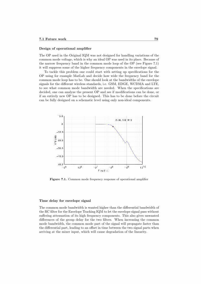
7.1 Future work 79
Design of operational amplifier
The OP used in the Original IQM was not designed for handling variations of thecommon mode voltage, which is why an ideal OP was used in its place. Because ofthe narrow frequency band in the common mode loop of the OP (see Figure 7.1)it will suppress some of the higher frequency components in the envelope signal.
To tackle this problem one could start with setting up specifications for theOP using for example MatLab and decide how wide the frequency band for thecommon mode loop has to be. One should look at the bandwidths of the envelopesignals for the different wireless standards, i.e. GSM, EDGE, WCDMA and LTE,to see what common mode bandwidth are needed. When the specifications aredecided, one can analyze the present OP and see if modifications can be done, orif an entirely new OP has to be designed. This has to be done before the circuitcan be fully designed on a schematic level using only non-ideal components.
Figure 7.1. Common mode frequency response of operational amplifier
Time delay for envelope signal
The common mode bandwidth is wanted higher than the differential bandwidth ofthe RC filter for the Envelope Tracking IQM to let the envelope signal pass withoutsuffering attenuation of its high frequency components. This also gives unwanteddifferences of the group delay for the two filters. When increasing the commonmode bandwidth, the common mode part of the signal will propagate faster thanthe differential part, leading to an offset in time between the two signal parts whenarriving at the mixer input, which will cause degradation of the linearity.

80 Conclusions
If one could find the time offset which is separating the common mode anddifferential signal parts, one should be able to insert a delay unit for the envelopesignal and thereby synchronizing the two signal parts.
7.1.2 Direct Voltage IQM
Both the Direct Voltage IQM and the Predistorted Direct Voltage IQM are dis-cussed in this section, as they are facing the same problems.
Investigate linearity in mixer
The thesis work has shown that linearity problems most definitely lies in thecurrent version of the mixer. As the predistortion of the Direct Voltage IQMdidn’t show the expected improvements, and results from simulations without themixer gave a clear improvement, much points at the mixer. Our suggestion forthe first work to be done on the Predistorted Direct Voltage IQM is observing themixer at a much lower LO frequency. This would reduce the negative effects fromthe parasitic capacitances of the switching transistors. Doing this and analyzingthe sizing of the transistors may result in the needed understanding for a muchbetter linearity improvement leading to lower current consumption.
Redesign the output stage
As the output stage was designed to have an input swing of 600 mV but the DirectVoltage IQM only has a voltage swing of 400 mV the expected SNR is not achievedin the output stage. Simply redesigning the cascade output stage using the noiseanalysis from Section 5.2.1 as a background, one could possibly improve the SNRin the circuit.
Optimize the 4PGFD circuit
As the clock generator we used was previously designed for another circuit, it wasnot optimized at all for this application. The authors of [24] described in theirarticle a way to create the wanted clock signals by some divide-by-two circuitscombined with some logic. Designing a small clock driver with lower currentconsumption and lower noise generation would help increase the performance ofthe Direct Voltage IQM.
7.2 Final words 81
7.2 Final words
As an ending for this thesis report we want to say that we have learned a greatdeal during our time at ST-Ericsson. One of the bigger lessons learned is theimportance of regularly taking a step back when working with a complex designand have another look at the problem from a higher hierarchical level. This ensuresthat one does not lose focus on the actual problem when working at a low level withspecific tasks. Using different methods and taking advantage of other people’s ideaswill help to get a better understanding and a good overview of the full problem.Another thing to take into concern is the fact that mistakes are always made.Making ’sanity-checks’ from time to time will hopefully reveal the made mistakessooner rather than later and reduce their impact on the work. This is somethingwe now more than ever will carry with us.
Finally, one very interesting thought that has been discussed, is the combina-tion of the two different types of IQ modulator circuits. Matching an amplifiercircuit to the Predistorted Direct Voltage IQM, it may be possible to implementenvelope tracking for this IQM as well. This combination should theoretically givea SAW-less design with a significant reduction of the current consumption, espe-cially for the future LTE technology. We can certainly say that this thesis hasopened up possibilities for future winnings.

Bibliography
[1] 3GPP. LTE. February 2010. URL: http://www.3gpp.org/LTE.
[2] 3GPP. UMTS. February 2010. URL: http://www.3gpp.org/article/umts.
[3] Roy Blake. Electronic Communication Systems. Delmar, 2nd edition, 2002.ISBN 0-7668-2684-8.
[4] Patrick Savelli Emmanuel Seurre and Pierre-Jean Pietri. GPRS for MobileInternet (Mobile Communications Library). Artech House Publishers, 2003.ISBN 1-58053-600-X.
[5] Johan Sköld Erik Dahlman, Stefan Parkvall and Per Beming. 3G Evolution.Academic Press, 2007. ISBN 978-0-12-372533-2.
[6] Center for Wireless Telecommunications. GSM. October 2002. URL:http://www.cwt.vt.edu/faq/gsm.htm.
[7] Andrea Goldsmith. Wireless communications. Cambridge University Press,2005.
[8] Harri Holma and Antti Toskala, editors. WCDMA for UMTS: HSPA evolutionand LTE. John Wiley & Sons, Ltd, 4th edition, 2007. ISBN 978-0-470-31933-8.
[9] Junsung Lim Hyung G. Myung and David J. Goodman. Sin-gle Carrier FDMA for Uplink Wireless Transmission. ieeex-plore.ieee.org/iel5/10209/4099336/04099344.pdf, 2006.
[10] National Instruments. What is I/Q Data? Version 14, 14 April 2009. URL:ftp://ftp.ni.com/pub/devzone/pdf/tut_4805.pdf.
[11] David A. Johns and Ken Martin. Analog Integrated Circuit Design. JohnWiley & Sons, Inc., 1st edition, 1997. ISBN 0-471-14448-7.
[12] Jon Legarda. Feedforward amplifier for wideband communication systems.Springer, 1st edition, 2006. ISBN 038735137X.
[13] II Leon W. Couch. Digital and Analog Communication Systems. PearsonEducation International, 6th edition, 2002.
83

84 Bibliography
[14] Stephen A. Maas. Nonlinear Microwave and RF Circuits. Artech House, 2ndedition, 2003. ISBN 1580534848.
[15] University of Hull. Electromagnetic Compatibility Aspects Of Future Radio-Based Mobile Telecommunication Systems, Appendix D - Digital Modulationand GMSK. http://www.emc.york.ac.uk/reports/linkpcp/appD.pdf, 1999.
[16] University of Toronto. GSM900. http://www.azizi.ca/gsm/modulation/index.html,2010.
[17] John G. Proakis. Digital Communications. McGraw-Hill Professional, 3rdedition, 1995. ISBN 0-07-113814-5.
[18] Clint Smith and Daniel Collins. 3G Wireless Networks. McGraw-Hill Profes-sional, 2nd edition, 2007. ISBN 0-07-226344-X.
[19] Issam Toufik Stefania Sesia and Matthew Baker, editors. LTE, The UMTSLong Term Evolution: From Theory to Practice. John Wiley & Sons, Ltd,2009. ISBN 978-0-470-69716-0.
[20] Javier Romero Timo Halonen and Juan Melero. GSM, GPRS, and EdgePerformance: Evolution Towards 3G/UMTS. John Wiley & Sons, Ltd, 2003.ISBN 0-470-86694-2.
[21] TutorialsPoint.COM. The GSM Specifications. February 2010. URL:http://www.tutorialspoint.com/gsm/gsm_specification.htm.
[22] K. A. Jose V. K. Varadan, Kalarickaparambil Joseph Vinoy. RF MEMS andtheir applications. John Wiley and Sons, 2003. ISBN 047084308X.
[23] Bernhard H. Walke. Mobile Radio Networks: Networking, Protocols andTraffic Performance. John Wiley & Sons, Ltd, 2nd edition, 2002. ISBN 0471-49902-1.
[24] Jan van Sinderen Xin He. A 45nm Low-Power SAW-less WCDMA TransmitModulator Using Direct Quadrature Voltage Modulation. ISSCC 2009.
[25] Peter Asbeck Xuejun Zhang, Lawrence E. Larson. Design of Linear RF Out-phasing Power Amplifiers. Artech House, 2003. ISBN 1580533744.
Upphovsrätt
Detta dokument hålls tillgängligt på Internet — eller dess framtida ersättare —under 25 år från publiceringsdatum under förutsättning att inga extraordinäraomständigheter uppstår.
Tillgång till dokumentet innebär tillstånd för var och en att läsa, ladda ner,skriva ut enstaka kopior för enskilt bruk och att använda det oförändrat för icke-kommersiell forskning och för undervisning. Överföring av upphovsrätten vid ensenare tidpunkt kan inte upphäva detta tillstånd. All annan användning av doku-mentet kräver upphovsmannens medgivande. För att garantera äktheten, säkerhe-ten och tillgängligheten finns det lösningar av teknisk och administrativ art.
Upphovsmannens ideella rätt innefattar rätt att bli nämnd som upphovsmani den omfattning som god sed kräver vid användning av dokumentet på ovan be-skrivna sätt samt skydd mot att dokumentet ändras eller presenteras i sådan formeller i sådant sammanhang som är kränkande för upphovsmannens litterära ellerkonstnärliga anseende eller egenart.
För ytterligare information om Linköping University Electronic Press se förla-gets hemsida http://www.ep.liu.se/
Copyright
The publishers will keep this document online on the Internet — or its possi-ble replacement — for a period of 25 years from the date of publication barringexceptional circumstances.
The online availability of the document implies a permanent permission foranyone to read, to download, to print out single copies for his/her own use andto use it unchanged for any non-commercial research and educational purpose.Subsequent transfers of copyright cannot revoke this permission. All other uses ofthe document are conditional on the consent of the copyright owner. The publisherhas taken technical and administrative measures to assure authenticity, securityand accessibility.
According to intellectual property law the author has the right to be mentionedwhen his/her work is accessed as described above and to be protected againstinfringement.
For additional information about the Linköping University Electronic Pressand its procedures for publication and for assurance of document integrity, pleaserefer to its www home page: http://www.ep.liu.se/
c© Mattias Johansson, Jonas Ehrs