
In situ observation of graphene sublimation and multi ... · In situ observation of graphene...
6
In situ observation of graphene sublimation and multi-layer edge reconstructions Jian Yu Huang a,1 , Feng Ding b,c , Boris I. Yakobson c,1 , Ping Lu d , Liang Qi e , and Ju Li e,1 a Center for Integrated Nanotechnologies, Sandia National Laboratories, Albuquerque, NM 87185; b Institute of Textiles and Clothing, Hong Kong Polytechnic University, Kowloon, Hong Kong, People’s Republic of China; c Department of Mechanical Engineering and Materials Science, and the Department of Chemistry, Rice University, Houston, TX 77005; d Sandia National Laboratories, Mail Stop 1411, Albuquerque, NM 87185; and e Department of Materials Science and Engineering, University of Pennsylvania, Philadelphia, PA 19104 Communicated by Sumio Iijima, Meijo University, Nagoya, Japan, May 13, 2009 (received for review January 19, 2009) We induced sublimation of suspended few-layer graphene by in situ Joule-heating inside a transmission electron microscope. The graphene sublimation fronts consisted of mostly {1100} zigzag edges. Under appropriate conditions, a fractal-like ‘‘coastline’’ morphology was observed. Extensive multiple-layer reconstruc- tions at the graphene edges led to the formation of unique carbon nanostructures, such as sp 2 -bonded bilayer edges (BLEs) and nano- tubes connected to BLEs. Flat fullerenes/nanopods and nanotubes tunneling multiple layers of graphene sheets were also observed. Remarkably, >99% of the graphene edges observed during sub- limation are BLEs rather than monolayer edges (MLEs), indicating that BLEs are the stable edges in graphene at high temperatures. We reproduced the ‘‘coastline’’ sublimation morphologies by ki- netic Monte Carlo (kMC) simulations. The simulation revealed geometrical and topological features unique to quasi-2-dimen- sional (2D) graphene sublimation and reconstructions. These re- constructions were enabled by bending, which cannot occur in first-order phase transformations of 3D bulk materials. These results indicate that substrate of multiple-layer graphene can offer unique opportunities for tailoring carbon-based nanostructures and engineering novel nano-devices with complex topologies. flat fullerene fractal sublimation graphene bilayer edge in situ electron microscopy fractional nanotube I magine burning a piece of paper: The reaction front tends to be jagged. Furthermore, if one examines the ashes left behind, most are curved. This is because paper, being a thin 2-dimen- sional (2D) object, is easy to bend. Here, we report an analogous experiment, but on graphene instead of ordinary paper, and at the nanoscale inside a high-resolution transmission electron microscope (HRTEM). We induced the sublimation of sus- pended multilayer graphene by Joule-heating, so it becomes thermodynamically favorable for carbon atoms to escape into the gas phase, leaving freshly exposed (open) edges on the solid graphene. The remaining graphene edges curled up under observation, and often welded together. We attribute this be- havior to the driving force to reduce dangling bonds on the edges (capillary energy), at the cost of bending energy. The sublima- tion of few-layer graphene, such as a 10-layer stack, is particu- larly interesting compared with the sublimation of monolayer graphene. In few-layer graphene, different layers often sponta- neously fuse together, forming nanostructures in situ, on top of 1 or 2 electrically conductive, extended, graphene sheets. During Joule heating, both the f lat graphene sheet and the self-wrapping nanostructures, like bilayer edges (BLEs) (1) and nanotubes (2, 3) interconnected to BLEs, have unique electronic properties important for device applications. However, the biggest obstacle to exploiting the extraordinary properties of graphene or carbon nanotubes etc., is to control their nanostructure and assembly. The in situ self-assembly process we observed leads to new understanding of carbon nanostructure formation and may eventually lead to a new paradigm for engineering integrated carbon-based devices (4–16). Results and Discussion Graphene samples were prepared using a Scotch tape peeling method similar to that reported in the literature (4 –7, 9, 10). (For details see Fig. S1) In brief, individual graphene was mounted on a TEM grid, and was connected by a scanning tunneling micros- copy (STM) tip, using a Nanofactory TEM-STM platform (17, 18). TEM observations were conducted in a Tecnai F30 analyt- ical electron microscope operated at 300 kV. A STM probe was manipulated to contact individual graphene with a layer thick- ness of 10 layers (Fig. 1A), followed by Joule-heating of the graphene to high temperatures by applying a bias voltage of 2.5 V. Once a high current was passed through the graphene layers, its crystalline quality and surface cleanness were improved. Fig. 1B shows a Joule-heated graphene with 10 layers. [Each fringe in fact corresponds to a bilayer (1); for details, see Figs. 3B, 4, and 5]. The surface was very clean and free of amorphous materials. The maximum current density flowing in a graphene layer was similar to that in a carbon nanotube, 10 8 A/cm 2 (19–24). From this current density and the sublimation temper- ature of graphite in high vacuum (25), we estimated that the temperature in the Joule heated graphene is 2000 °C, which is similar to the temperatures in Joule-heated carbon nanotubes (26). At high temperatures and under electron beam irradiation, sublimation of graphene took place. The sublimation is predom- inantly caused by Joule-heating, but facilitated by electron beam irradiation. Without Joule-heating, few layer graphene turned into highly disordered or even amorphous structure. The sublimation front consisted predominantly of zigzag edges, and very rarely of the armchair or other high-index-plane edges. Fig. 1 C–E and Movie S1 show sequential HRTEM images of the evolution of a sublimation edge. The graphene was close to the [0001] orientation, as seen from a Fast Fourier Transfor- mation (Fig. 1 F). The sublimation created a nano-hole or void with a 60°-angular-tip formed by 2 intersecting zigzag planes, and the void propagated along the (10 –10) and (01–10) zigzag edges (Fig. 1C). Occasionally, the void propagated along a (1–210) armchair edge (Fig. 1D), but this lasted for only a few seconds, and the void then propagated back to the zigzag edges (Fig. 1 E). During the void propagation, kink motions along the zigzag edges occurred (pointed out by arrowheads in Fig. 1 C and E). The kink, marked as ‘‘SK’’ (Fig. 1 E), ‘‘DK’’ (Fig. 1 C and 1 E), and ‘‘TK’’ (Fig. 1C), is 1, 2, and 3 atomic rows high, respectively, which could nucleate from anywhere on the zigzag edges, then propagated along the same edges. After each kink swept through, 1 or a few zigzag atomic rows were eliminated. This Author contributions: J.Y.H. and J.L. designed research; J.Y.H., F.D., P.L., L.Q., and J.L. performed research; J.Y.H., P.L., L.Q., and J.L. contributed new reagents/analytic tools; J.Y.H., F.D., B.I.Y., P.L., L.Q., and J.L. analyzed data; and J.Y.H., F.D., P.L., L.Q., and J.L. wrote the paper. The authors declare no conflict of interest. 1 To whom correspondence may be addressed. E-mail: [email protected], [email protected], or [email protected]. This article contains supporting information online at www.pnas.org/cgi/content/full/ 0905193106/DCSupplemental. www.pnas.orgcgidoi10.1073pnas.0905193106 PNAS Early Edition 1 of 6 ENGINEERING
Transcript of In situ observation of graphene sublimation and multi ... · In situ observation of graphene...
In situ observation of graphene sublimation andmulti-layer edge reconstructionsJian Yu Huanga,1, Feng Dingb,c, Boris I. Yakobsonc,1, Ping Lud, Liang Qie, and Ju Lie,1
aCenter for Integrated Nanotechnologies, Sandia National Laboratories, Albuquerque, NM 87185; bInstitute of Textiles and Clothing, Hong KongPolytechnic University, Kowloon, Hong Kong, People’s Republic of China; cDepartment of Mechanical Engineering and Materials Science, and theDepartment of Chemistry, Rice University, Houston, TX 77005; dSandia National Laboratories, Mail Stop 1411, Albuquerque, NM 87185; andeDepartment of Materials Science and Engineering, University of Pennsylvania, Philadelphia, PA 19104
Communicated by Sumio Iijima, Meijo University, Nagoya, Japan, May 13, 2009 (received for review January 19, 2009)
We induced sublimation of suspended few-layer graphene by insitu Joule-heating inside a transmission electron microscope. Thegraphene sublimation fronts consisted of mostly {1100} zigzagedges. Under appropriate conditions, a fractal-like ‘‘coastline’’morphology was observed. Extensive multiple-layer reconstruc-tions at the graphene edges led to the formation of unique carbonnanostructures, such as sp2-bonded bilayer edges (BLEs) and nano-tubes connected to BLEs. Flat fullerenes/nanopods and nanotubestunneling multiple layers of graphene sheets were also observed.Remarkably, >99% of the graphene edges observed during sub-limation are BLEs rather than monolayer edges (MLEs), indicatingthat BLEs are the stable edges in graphene at high temperatures.We reproduced the ‘‘coastline’’ sublimation morphologies by ki-netic Monte Carlo (kMC) simulations. The simulation revealedgeometrical and topological features unique to quasi-2-dimen-sional (2D) graphene sublimation and reconstructions. These re-constructions were enabled by bending, which cannot occur infirst-order phase transformations of 3D bulk materials. Theseresults indicate that substrate of multiple-layer graphene can offerunique opportunities for tailoring carbon-based nanostructuresand engineering novel nano-devices with complex topologies.
flat fullerene � fractal sublimation � graphene bilayer edge � in situelectron microscopy � fractional nanotube
Imagine burning a piece of paper: The reaction front tends tobe jagged. Furthermore, if one examines the ashes left behind,
most are curved. This is because paper, being a thin 2-dimen-sional (2D) object, is easy to bend. Here, we report an analogousexperiment, but on graphene instead of ordinary paper, and atthe nanoscale inside a high-resolution transmission electronmicroscope (HRTEM). We induced the sublimation of sus-pended multilayer graphene by Joule-heating, so it becomesthermodynamically favorable for carbon atoms to escape into thegas phase, leaving freshly exposed (open) edges on the solidgraphene. The remaining graphene edges curled up underobservation, and often welded together. We attribute this be-havior to the driving force to reduce dangling bonds on the edges(capillary energy), at the cost of bending energy. The sublima-tion of few-layer graphene, such as a 10-layer stack, is particu-larly interesting compared with the sublimation of monolayergraphene. In few-layer graphene, different layers often sponta-neously fuse together, forming nanostructures in situ, on top of1 or 2 electrically conductive, extended, graphene sheets. DuringJoule heating, both the flat graphene sheet and the self-wrappingnanostructures, like bilayer edges (BLEs) (1) and nanotubes (2,3) interconnected to BLEs, have unique electronic propertiesimportant for device applications. However, the biggest obstacleto exploiting the extraordinary properties of graphene or carbonnanotubes etc., is to control their nanostructure and assembly.The in situ self-assembly process we observed leads to newunderstanding of carbon nanostructure formation and mayeventually lead to a new paradigm for engineering integratedcarbon-based devices (4–16).
Results and DiscussionGraphene samples were prepared using a Scotch tape peelingmethod similar to that reported in the literature (4–7, 9, 10). (Fordetails see Fig. S1) In brief, individual graphene was mounted ona TEM grid, and was connected by a scanning tunneling micros-copy (STM) tip, using a Nanofactory TEM-STM platform (17,18). TEM observations were conducted in a Tecnai F30 analyt-ical electron microscope operated at 300 kV. A STM probe wasmanipulated to contact individual graphene with a layer thick-ness of �10 layers (Fig. 1A), followed by Joule-heating of thegraphene to high temperatures by applying a bias voltage of �2.5V. Once a high current was passed through the graphene layers,its crystalline quality and surface cleanness were improved. Fig.1B shows a Joule-heated graphene with 10 layers. [Each fringein fact corresponds to a bilayer (1); for details, see Figs. 3B, 4,and 5]. The surface was very clean and free of amorphousmaterials. The maximum current density flowing in a graphenelayer was similar to that in a carbon nanotube, �108 A/cm2
(19–24). From this current density and the sublimation temper-ature of graphite in high vacuum (25), we estimated that thetemperature in the Joule heated graphene is �2000 °C, which issimilar to the temperatures in Joule-heated carbon nanotubes(26). At high temperatures and under electron beam irradiation,sublimation of graphene took place. The sublimation is predom-inantly caused by Joule-heating, but facilitated by electron beamirradiation. Without Joule-heating, few layer graphene turnedinto highly disordered or even amorphous structure.
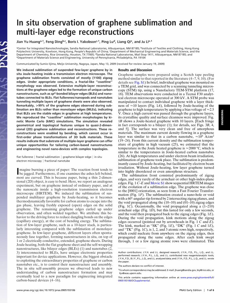
The sublimation front consisted predominantly of zigzagedges, and very rarely of the armchair or other high-index-planeedges. Fig. 1 C–E and Movie S1 show sequential HRTEM imagesof the evolution of a sublimation edge. The graphene was closeto the [0001] orientation, as seen from a Fast Fourier Transfor-mation (Fig. 1F). The sublimation created a nano-hole or voidwith a 60°-angular-tip formed by 2 intersecting zigzag planes, andthe void propagated along the (10–10) and (01–10) zigzag edges(Fig. 1C). Occasionally, the void propagated along a (1–210)armchair edge (Fig. 1D), but this lasted for only a few seconds,and the void then propagated back to the zigzag edges (Fig. 1E).During the void propagation, kink motions along the zigzagedges occurred (pointed out by arrowheads in Fig. 1 C and E).The kink, marked as ‘‘SK’’ (Fig. 1E), ‘‘DK’’ (Fig. 1 C and 1E),and ‘‘TK’’ (Fig. 1C), is 1, 2, and 3 atomic rows high, respectively,which could nucleate from anywhere on the zigzag edges, thenpropagated along the same edges. After each kink sweptthrough, 1 or a few zigzag atomic rows were eliminated. This
Author contributions: J.Y.H. and J.L. designed research; J.Y.H., F.D., P.L., L.Q., and J.L.performed research; J.Y.H., P.L., L.Q., and J.L. contributed new reagents/analytic tools;J.Y.H., F.D., B.I.Y., P.L., L.Q., and J.L. analyzed data; and J.Y.H., F.D., P.L., L.Q., and J.L. wrotethe paper.
The authors declare no conflict of interest.
1To whom correspondence may be addressed. E-mail: [email protected], [email protected], [email protected].
This article contains supporting information online at www.pnas.org/cgi/content/full/0905193106/DCSupplemental.
www.pnas.org�cgi�doi�10.1073�pnas.0905193106 PNAS Early Edition � 1 of 6
ENG
INEE
RIN
G

rendered graphene with predominantly zigzag edges, connectedby small armchair edge segments (e.g., the irregular edgespointed out by arrows in Fig. 1D).
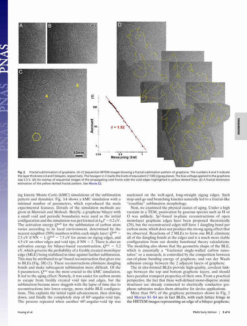
Fig. 2 (Movie S2) shows a fractal-like overall sublimationpattern (27). There are 10 layers in this graphene, determinedfrom the lattice fringes of the graphene edges (Fig. 1B). Initially,a main void (Fig. 2 A) with some small secondary voids appearedin one of the 5 bilayers. The main void and its secondary voidsall grew with the lapse of time (Fig. 2B). Simultaneously, newvoids were nucleated on the side faces of existing ones and thepropagation directions can change to new sets of zigzag planes.Similarly, the next generations of voids nucleated and grew, until
a fractal-like pattern emerged (Fig. 2C). Most of the voidspropagated along one of the 6 equivalent {1100} zigzag edges,and in a very rare occasion, a void propagated along a {1120}armchair edge. From the overlaid sequential images of thesublimation fronts (Fig. 2D), we calculated the fractal dimensionof the ‘‘coastline’’ pattern (28) to be 1.52 (Fig. 2E, details of thefractal dimension calculation are in Fig. S2). In comparison, thewell-known Sierpinski triangle sieve has fractal dimension 1.58; andthe Sierpinski hexagon, which has hexagonal symmetry, has fractaldimension 1.63 (www.tgmdev.be/curvesierpinskiobj.htm).
This intriguing local zigzag-edge preference and the resultingglobal ‘‘coastline’’ morphologies can be understood by perform-
A B
C
D
E
F
Fig. 1. In situ TEM images showing a graphene sublimation pattern. (A) A TEM image showing a graphene sheet mounted on a TEM grid connected with anSTM probe. (B) A HRTEM image of a 10-layer (5-bilayer) graphene. The graphene was Joule-heated to high temperatures by applying a bias voltage of �2.5 V.(C–E) Sequential HRTEM images showing the propagation of one void created by atom sublimation. The numbers 4 and 5 indicate the layer thickness being 4and 5 bilayers, respectively. The arrowheads and SK, DK, and TK pointed out single, double, and triple atomic-plane-thick kinks on the BLEs, respectively. Arrowsin D point out armchair edges. (F) A Fast Fourier Transformation of the graphene shown in C–E.
2 of 6 � www.pnas.org�cgi�doi�10.1073�pnas.0905193106 Huang et al.
ing kinetic Monte Carlo (kMC) simulations of the sublimationpattern and dynamics. Fig. 3A shows a kMC simulation with aminimal number of parameters, which reproduced the mainexperimental features. Details of the simulation methods aregiven in Materials and Methods. Briefly, a graphene bilayer witha small void and periodic boundaries were used as the initialconfiguration and the simulation was performed at kBT � 0.2 eV.The activation energy Qsub for the sublimation of carbon atomvaries according to its local environment, determined by thenearest neighbor (NN) numbers within each single layer: Qsub �2.5 eV if NN � 1; Qsub � 7.5 eV for atoms on zigzag edges, and4.5 eV on other edges and void tips, if NN � 2. There is also anactivation energy for bilayer-based reconstruction, Qrec � 5.2eV, which governs the probability of a freshly created monolayeredge (MLE) being stabilized in time against further sublimation.This may be attributed to sp2-based reconstruction that gives riseto BLEs (Fig. 3B) (1). These reconstructions eliminate danglingbonds and make subsequent sublimation more difficult. Of the4 parameters, Qrec was the most crucial to the kMC simulation.It led to the aging effect: Namely, it was easier for carbon atomsto escape from freshly created void tips and edges, but thesublimation became more sluggish with the lapse of time due toreconstructions into lower-energy, more stable BLE configura-tions. This explains the initial rapid advancement, then slowingdown, and finally the completely stop of 60°-angular-void tips.The process repeated when another 60°-angular-void tip was
nucleated on the well-aged, long-straight zigzag edges. Suchstop-and-go and branching kinetics naturally led to a fractal-like‘‘coastline’’ sublimation morphology.
Next, we examined the physical causes of aging. Under a highvacuum in a TEM, passivation by gaseous species such as H orO was unlikely. Sp2-based in-plane reconstructions of openmonolayer graphene edges have been proposed theoretically(29), but the reconstructed edges still have 1 dangling bond percarbon atom, which does not produce the strong aging effect thatwe observed. Reactions of 2 MLEs to form one BLE eliminateall of the dangling bonds at the edges and is a much more stableconfiguration from our density functional theory calculations.The modeling also shows that the geometric shape of the BLE,which is essentially a ‘‘fractional single-walled carbon nano-tubes’’ or a nanoarch, is controlled by the competition betweenout-of-plane bending energy of graphene, and van der Waalsadhesion energy between the 2 adjacent layers of graphene.
The in situ-formed BLEs provide high-quality, covalent link-age between the top and bottom graphene layers, and shouldhave peculiar transport properties of their own. From a practicalperspective, the fact that these well-defined mono-disperse atomicstructures are already connected to electrically conductive gra-phene substrates makes them attractive for device applications.
More than 99% of the graphene perimeters shown in Fig. 2and Movies S1–S4 are in fact BLEs, with each lattice fringe inthe HRTEM images representing an edge of a bilayer graphene,
4
5
A B
C
D
E
Fig. 2. Fractal sublimination of graphene. (A–C) Sequential HRTEM images showing a fractal sublimation pattern of graphene. The numbers 4 and 5 indicatethe layer thickness is 4 and 5 bilayers, respectively. The hexagon in C marks the 6 sets of equivalent {1100} zigzag planes. The bias voltage applied to the graphenewas 2.5 V. (D) An overlay of sequential images of the propagating void fronts with the void edges highlighted in yellow-dotted lines. (E) A fractal dimensionestimation of the yellow-dotted fractal pattern. See Movie S2.
Huang et al. PNAS Early Edition � 3 of 6
ENG
INEE
RIN
G

the structures of which were reported by Liu et al. (1). Fig. 4 andMovie S3 show direct evidence of the existence of a BLE. A voidinitially appeared on the top layer (Fig. 4 A and E), and migratedtoward the edge of the bilayer (Fig. 4 B and F), then the bottom
layer (shown in blue in Fig. 4) sublimated. As the bottom layersublimated, its trailing edge bonded with the top layer (pointedout by green arrows in Fig. 4C, D, and G), forming BLEs in situ.Existence of similar bilayers was reported in heat-treated graph-ite (1), indicating that a BLE rather than a MLE is the morestable structural unit in a multiple-layer graphene. The resultshave important implications in the device applications of gra-phene: When one designs a graphene-based device, one mustconsider the possibility that the device operates with a BLE (Fig.3B), rather than with a MLE. These BLEs may be misinterpretedas MLEs in a recent report (16).
In addition to BLEs that may serve as well-defined 1D devicecomponents, we have also found many other types of intercon-nected nanostructures. Fig. 5 A–C and Movie S4 show the in situformation of a single-walled nanotube that bridges two BLEs.Fig. 5D illustrates the geometry of the final product, which isbased entirely on sp2 bonding. Such complex topology, formedin situ, is only possible in 2D layered materials, where bendingis easy. Generally speaking, we interpret the spontaneous for-mation of various interconnected carbon nanostructures aspathways for graphene to reduce its capillary energy. Fig. 5 E–Hand Fig. S3 show the in situ formation of a single-wallednanotube by the wrapping or rolling of a graphene ribbon, whilestill connecting to a bilayer graphene. The tube appears to bevery flexible and can bend to large angles (Fig. S3). Again, thesecoherently interconnected carbon nanostructures with electricalleads in and out might be useful from device and processingconsiderations.
The stability of some of the interconnected carbon nanostruc-tures is astonishing (Movie S4). Once formed, they maintainedtheir nanostructures despite the flat graphene around themhaving lower carbon chemical potential (no bending elasticenergy and no topological defects) and are in the process ofsublimation. The extreme limits of this metastability are the fullyencapsulated nanopods/f lat fullerenes (Fig. 5 I–M, Fig. S4, andMovie S4) that formed in situ, which apparently made randomwalks (framed area in Movie S4) on the graphene surfacewithout growing, shrinking, or changing their shape whereas thegraphene matrix rapidly receded in front of it (Fig. S4E andMovie S4). We attribute such metastability to the elimination offree edges, making subsequent sublimation kinetically difficult.Therefore, the driving force for creating the interconnectedcarbon nanostructures, e.g., reduction of capillary energy by
90nm
A
B
Fig. 3. Kinetic Monta Carlo simulation of fractal sublimination of graphene.(A) A graphene sublimation pattern obtained from a kMC calculation after120,000 simulation steps. Only atoms on the graphene edges are shown. (B)schematic of a zigzag BLE of graphene (1).
A B C D
E F G
Fig. 4. Experimental evidence of graphene BLEs. (A–D) Sequential HRTEM images proving the existence of BLEs of graphene (Movie S3). Yellow-dotted linespoint out the edge of a monolayer vacancy hole on the top-layer. The blue-dotted lines pointed out the monolayer edge of the bottom layer. Green arrowsdenote the reconstructed BLEs. (E–G) Schematic drawings corresponding to (A–C), respectively, showing the zipping up of MLEs to BLEs.
4 of 6 � www.pnas.org�cgi�doi�10.1073�pnas.0905193106 Huang et al.

bending and curling enabled reconstructions, also protectedthem from further sublimation.
In summary, we observed the following sequence of salientfeatures during graphene sublimation: (i) creation of open edges(high capillary energies) on 1 or 2 adjacent layers of graphene byexternal energy; (ii) large spontaneous conformational (30) andtopological changes of the remaining graphene, which we at-tribute to bending to reduce the high capillary energy of openedges; and (iii) in situ formation of metastable nanostructures,interconnected to 1 or 2 or multiple layers of extended graphenevia sp2 carbon-carbon bonds with large out-of-plane curvature.The process of (ii) is unique to quasi-2D systems, which has asmall bending modulus and bending gives rise to unique mor-phologies, kinetics and products fundamentally very different
from the 3D bulk systems. Controlled fabrication of these carbonnanostructures on few-layer graphene substrates and in-depthstudies of their electronic properties may lead to production ofnew carbon-based nanoelectronic devices.
Materials and MethodsTEM Sample Preparation Procedures. Highly orientated pyrolytic graphite(HOPG) with a thickness of a few hundred �m was glued to a glass slide witha double-sided adhesive tape (Fig. S1A). The HOPG was thinned down totransparent under an optical microscope by repeated peeling using a Scotchtape (Fig. S1B). A 200-mesh transmission electron microscopy (TEM) grid wascut into half, painted with conducting silver epoxy on the grid bars, and thenglued on the transparent graphene sheet on the glass slide. Once the silverepoxy was cured, the half grid was lifted off from the glass slide (Fig. S1C).Graphene was attached to the grid (sketched in dark) after lifting off from the
V
V
V
0.543 nm 0.339 nm
1
2
A
B
C
D
E
F
G
H
I J
K
L
M
Fig. 5. Carbon nanostructures formed in situ on graphene substrate by Joule-heating. (A–D) Two neighboring bilayer graphene interconnected by a carbonnanotube (pointed out by arrowheads in (A–C). (E–G) HRTEM images of interconnected graphene layers. The red- and blue-dotted lines point out BLEs and aMLE, respectively. Schematic drawing of BLEs and MLEs are shown in (E–G). The pink arrows in F and G point out carbon nanotubes connected to a bilayergraphene, a schematic drawing of which is shown in H. Note each dark fringe in (E–G) may represent either a BLE or a MLE. The determination of the structuralconfigurations of each fringe is described in Fig. S3. (I and J) Sequential HRTEM images showing the formation of a nano-pod/flat fullerene. The numbers ‘‘1’’and ‘‘2’’ indicate the layer thickness being 1 and 2 layers, respectively. A green-dotted line in I marks a MLE. The monolayer graphene sublimated and thenreconstructed with a neighboring graphene edge, forming a nanopod/flat fullerene. Detailed formation process of the nanopod/flat fullerene is described inFig. S4. (K–M) Structural models of a nanopod/flat fullerene in a side view (K), cross-section view (L), and top view (M), respectively.
Huang et al. PNAS Early Edition � 5 of 6
ENG
INEE
RIN
G

glass slide (Fig. S1D). The half TEM grid was glued to an Au rod of 280 �m andinserted into a Nanofactory TEM–scanning tunneling microscopy (TEM-STM)platform (Fig. S1D), in which a full functional STM is integrated into a TEM sampleholder, allowing for in situ manipulation and measurements of individual gra-phene. The as-prepared samples had many graphene sheets attached to the Cugrid bars. Graphene sheets up to 100 �m long by 50 �m wide and with a layerthickness from a single layer to �20 layers of graphene could be found.
Fractal Dimension Measurement . The fractal dimension of the propagatingfront pattern was measured by the same method as that used to measure thefractal dimension of the coastline (28). First, a close loop was drawn by fittingthe experimental propagating sublimation front (Fig. S2 A and B). Then theclose loop was measured on a 2D square lattice. In the measurement, onlythose squares that intersect with the close loop were accounted (e.g., the graysquares in Fig. S2C). By varying the size of the squares, the number ofaccounted squares as a function of a square size (i.e., the measuring unit) wasplotted (Fig. S2D). According to the definition of the fractal dimension, thefractal dimension of the loop or the propagating loop is calculated as:
d � �dlog(N)d log(I)
where N is the number of the accounted squares and l is the size of the squaresor the measuring unit. For the propagating front shown in Fig. S2A, the fittedfractal dimension is 1.52.
Kinetic Monte Carlo (KMC) Simulation Procedures. In kinetic Monte Carlo (kMC)simulations, graphene bilayer with 1 small void (diameter �1 nm) and periodicboundary conditions were used as initial configurations. The kMC operationsoccurred only on graphene edge atoms, whose nearest neighbor (NN) atomsin a single layer are less than 3. In each sublimation step only 1 carbon atomis removed and its activation energy Qsub varies according to the local envi-ronment (NN number and edge types): Qsub � 2.5 eV when NN � 1; when NN �2, Qsub � 7.5 eV for zigzag edges and 4.5 eV for armchair edges and void tips.The type of edge is determined by the total summation number of nearestneighbors of nearest neighbors (NNNN) for the atoms on that edge: it is zigzag
edges when NNNN � 6 and armchair edges when NNNN � 5. Because of thisdefinition, a single step on a zigzag edge is considered as a small armchairedge and removed quickly in simulation. A void tip is defined as a 60o
–angular-tip formed by 2 crossing zigzag edges or a zigzag edge with �3 edgeatoms. In addition, there is some probability, with an activation energy Qrec �5.21 eV, for one atom on a freshly created less-stable edge (armchair, void tipor NN � 1) to reconstruct into a state as stable as those on a zigzag edge. Sucha reconstruction may result from a sp3 junction with the bottom graphenelayer, which exists in real experiments; and we assume that on a zigzag edgethe similar reconstruction occurs immediately after an edge creation, whichmay be the reason that initially Qsub of a zigzag edge is much larger than theother edges. After the catalog of reaction event i and the correspondingactivation energy Qi is built, a kMC simulation is performed with eventprobability pi � �i �exp(�Qi/kBT), where �i � 1.0 � 1013 s�1 and kBT � 0.2 eV.
HRTEM Image Simulation Methods. HREM image simulations were performedby multislice calculation using JEMS software, using the following electronoptical parameters: 300 KV acceleration voltage, spherical aberration of 1.2mm, beam convergence angle of 0.5 mrad, defocus-spread 10 nm and under-defocus of 99 nm. The thermal vibration of the C atoms was included in thecalculation by the Debye–Waller factor.
Note Added in Proof. It was brought to our attention that the surface ofgraphite polyhedral crystal was terminated in nanoarches (30, 31), similar tothe closed edges reported in ref. 1 and the BLEs reported in this paper. Theseobservations further assert that BLEs or closed edges, rather than MLEs oropen edges, are the stable edge configurations in general graphitic materials.
ACKNOWLEDGMENTS. This work was performed, in part, at the Center forIntegrated Nanotechnologies, a U.S. Department of Energy, Office of BasicEnergy Sciences user facility. Sandia National Laboratories is a multiprogramlaboratory operated by Sandia Corporation, a Lockheed-Martin Company, forthe U. S. Department of Energy under Contract No. DE-AC04–94AL85000. Thiswork was supported by National Science Foundation Grant CMMI-0728069,the Air Force Office of Scientific Research, Honda Research Institute U.S.A.,Department of Energy Contract DOE-DE-FG02-06ER46330, and Office of NavalResearch Contract N00014-05-1-0504 (to L.Q. and J.L.).
1. Liu Z, Suenaga K, Harris PJF, Iijima S (2009) Open and closed edges of graphene layers.Phys Rev Lett 102:015501.
2. Iijima S (1991) Helical microtubules of graphitic carbon. Nature 354:56–58.3. Iijima S, Ichihashi T (1993) Single-shell carbon nanotubes of 1-nm diameter. Nature
363:603–605.4. Novoselov KS, et al. (2004) Electric field effect in atomically thin carbon films. Science
306:666–669.5. Geim AK, Novoselov KS (2007) The rise of graphene. Nat Mater 6:183–191.6. Novoselov KS, et al. (2005) Two-dimensional atomic crystals. Proc Natl Acad Sci USA
102:10451–10453.7. Novoselov KS, et al. (2007) Room-temperature quantum hall effect in graphene.
Science 315:1379.8. Ohta T, Bostwick A, Seyller T, Horn K, Rotenberg E (2006) Controlling the electronic
structure of bilayer graphene. Science 313:951–954.9. Meyer JC, et al. (2007) The structure of suspended graphene sheets. Nature 446:60–63.
10. Novoselov KS, et al. (2005) Two-dimensional gas of massless Dirac fermions in gra-phene. Nature 438:197–200.
11. Li XL, Wang XR, Zhang L, Lee SW, Dai HJ (2008) Chemically derived, ultrasmoothgraphene nanoribbon semiconductors. Science 319:1229–1232.
12. Lee C, Wei XD, Kysar JW, Hone J (2008) Measurement of the elastic properties andintrinsic strength of monolayer graphene. Science 321:385–388.
13. Bunch JS, et al. (2007) Electromechanical resonators from graphene sheets. Science315:490–493.
14. Gass MH, et al. (2008) Free-standing graphene at atomic resolution. Nature Nanotech-nology 3:676–681.
15. Girit CO, et al. (2009) Graphene at the edge: Stability and dynamics. Science 323:1705–1708.
16. Jia XT, et al. (2009) Controlled formation of sharp zigzag and armchair edges ingraphitic nanoribbons. Science 323:1701–1705.
17. Huang JY, et al. (2006) Superplastic carbon nanotubes—Conditions have been discov-ered that allow extensive deformation of rigid single-walled nanotubes. Nature439:281.
18. Huang JY, Ding F, Yakobson BI (2008) Dislocation dynamics in multiwall carbonnanotubes. Phys Rev Lett 100:035503.
19. Yao Z, Kane CL, Dekker C (2000) High-field electrical transport in single-wall carbonnanotubes. Phys Rev Lett 84:2941–2944.
20. Collins PC, Arnold MS, Avouris P (2001) Engineering carbon nanotubes and nanotubecircuits using electrical breakdown. Science 292:706–709.
21. Huang JY, et al. (2005) Atomic-scale imaging of wall-by-wall breakdown andconcurrent transport measurements in multiwall carbon nanotubes. Phys Rev Lett94:236802.
22. Jin C, Suenaga K, Iijima S (2008) Direct evidence for lip-lip interactions in multiwalledcarbon nanotubes. Nano Res 1:434.
23. Jin CH, Suenaga K, Iijima S (2008) Plumbing carbon nanotubes. Nature Nanotechnol-ogy 3:17–21.
24. Jin C, Lan H, Suenaga K, Peng L, Iijima S (2008) Metal atom catalyzed enlargement offullerenes. Phys Rev Lett 101:176102.
25. Haines JR, Tsai CC (2002) Graphite Sublimation Tests for the Muon Collider/NeutrinoFactory Target Development Program. Available at www.osti.gov/dublincore/ecd/servlets/purl/814308-ZH5lf7/native/814308.pdf.
26. Huang JY (2007) In situ observation of quasimelting of diamond and reversiblegraphite-diamond phase transformations. Nano Lett 7:2335–2340.
27. Mandelbrot B (1983) The Fractal Geometry of Nature (W H Freeman & Co, SanFrancisco).
28. Sapoval B, Baldassarri A, Gabrielli (2004) A Self-stabilized fractality of seacoaststhrough damped erosion. Phys Rev Lett 93:098501.
29. Koskinen P, Malola S, Hakkinen H (2008) Self-passivating edge reconstructions ofgraphene. Phys Rev Lett 101:115502.
30. Shenoy VB, Reddy CD, Ramasubramaniam A, Zhang YW (2008) Edge-stress-inducedwarping of graphene sheets and nanoribbons. Phys Rev Lett 101:245501.
31. Gogotsi Y, Libera JA, Kalashnikov N, Yoshimura M (2000) Graphite polyhedral crystals.Science 290:317–320.
6 of 6 � www.pnas.org�cgi�doi�10.1073�pnas.0905193106 Huang et al.