Impact of Random Telegraph Noise on CMOS Logic Circuit ... · CMOS technology. Section IV–VI...
8
Impact of Random Telegraph Noise on CMOS Logic Circuit Reliability Takashi Matsumoto Department of Communications and Computer Engineering Kyoto University, Kyoto, Japan Email: [email protected] Kazutoshi Kobayashi Department of Electronics Kyoto Institute of Technology, Kyoto, Japan Hidetoshi Onodera Department of Communications and Computer Engineering Kyoto University, Kyoto, Japan Abstract—The leading edge products have a feature size of 22 nm in 2014. Designing reliable systems has become a big challenge in recent years. Transistor reliability has a great impact on highly-reliable CMOS circuit operations. Random telegraph noise is one of major recent transistor reliability concerns. First, recent researches on RTN and its impact on circuits are briefly summarized. Then the impact of RTN on CMOS logic circuit reliability is described based on our results from 65 nm and 40 nm test chips. Circuit designers can change various parameters such as operating voltage, transistor size, number of logic stages and substrate bias. The impact of these parameters is clarified in view of RTN-induced CMOS logic delay uncertainty. The impact of RTN can be a serious problem even for logic circuits when they are operated under low supply voltage. I. I NTRODUCTION Physical feature size of a transistor has been reduced contin- ually over time. Leading edge products have a feature size of 22 nm in 2014. Due to the device miniaturization, the number of transistors in one processor becomes as much as 4.31 billion in 2014[1]. On the other hand, designing reliable systems has become a big challenge in recent years[2], [3], [4], [5]. One of the dominant issues is a transistor performance variation. It can be classified into static variation and dynamic variation. Static variation is caused by LSI manufacturing process variation[6]. Dynamic variation is caused by an environmental noise and an intrinsic device noise. As an example of dynamic variation, jitter in oscillators can be caused by both environmental and intrinsic device noise[7], [8]. Another example of dynamic variation is an LSI performance fluctuation or a gradual LSI performance degradation. It is known as LSI reliability prob- lems. In this paper, we deal with a reliability problem caused by intrinsic noise in transistor. It is well known today that Hot Carrier Injection (HCI), Bias Temperature Instability (BTI)[9], [10], Time Dependent Dielectric Breakdown (TDDB), and Random Telegraph Noise (RTN)[11] are main issues in tran- sistor gate oxide reliability. Transistor reliability has a great impact on modern CMOS circuits[12] and the quality of the interface between gate oxide and silicon substrate is one of the key factors for highly-reliable circuit operations. Nitridation process of gate oxide is widely used after 65 nm CMOS technologies. The increase of the nitrogen content at the SiO 2 /Si interface promotes the Negative Bias Temper- ature Instability (NBTI)[13], [14]. When transistors degrade owing to NBTI, the propagation delay of combinational logics increases. The correct operation of a register may not be guaranteed under the gradual performance degradation by NBTI. A remarkable phenomenon regarding NBTI is that the degraded performance of a pMOS transistor recovers when the bias temperature stress applied to the gate oxide is removed or relaxed[15], [16], [17]. Despite the extensive research on NBTI, there is still a controversy over the NBTI mechanism due to its recovery phenomena[18], [19]. There is a strong demand for the practical compact model that can treat NBTI and other reliability issues at the circuit simulation level[20], [21]. It is indispensable for the compact model to monitor NBTI and other reliability issues at the circuit level[22]. RTN has attracted much attention in these years due to the continuous technology scaling. RTN appears as a temporal transistor performance fluctuation. It is reported that the im- pact of RTN-induced fluctuation may exceed manufacturing process variation in 22 nm technology[23]. RTN is considered to share some common mechanisms with NBTI because RTN is caused by the capture and emission of mobile charged carriers. This paper summarizes recent researches on RTN and introduces our results from 65 nm and 40 nm test chips. Section II describes recent researches on RTN and its impact on circuits. Section III describes typical measurement results of RTN-induced transistor drain current fluctuation in a 65 nm CMOS technology. Section IV–VI describe the impact of RTN on CMOS logic circuit reliability followed by conclusion. II. RTN AND ITS I MPACT ON CIRCUITS Low frequency noise or 1/f noise is observed in various systems[24]. As for LSI systems, 1/f noise can be observed as a drain current fluctuation in a transistor with moderately large gate area. On the other hand, RTN is observed in a small transistor with a few oxide traps. RTN is characterized by a 1/f 2 spectrum that is called the Lorentzian power spectrum. One possible interpretation is that the superposition of various RTN (with a broad distribution of activation energies in RTN trap in gate oxide mobile charged carrier t rap in gate oxide m obile charged carrier Fig. 1. Capture and emission of carriers by gate oxide traps (nMOS).
Transcript of Impact of Random Telegraph Noise on CMOS Logic Circuit ... · CMOS technology. Section IV–VI...
Impact of Random Telegraph Noise on CMOSLogic Circuit Reliability
Takashi MatsumotoDepartment of Communications
and Computer EngineeringKyoto University, Kyoto, Japan
Email: [email protected]
Kazutoshi KobayashiDepartment of Electronics
Kyoto Institute of Technology, Kyoto, Japan
Hidetoshi OnoderaDepartment of Communications
and Computer EngineeringKyoto University, Kyoto, Japan
Abstract—The leading edge products have a feature size of22 nm in 2014. Designing reliable systems has become a bigchallenge in recent years. Transistor reliability has a great impacton highly-reliable CMOS circuit operations. Random telegraphnoise is one of major recent transistor reliability concerns. First,recent researches on RTN and its impact on circuits are brieflysummarized. Then the impact of RTN on CMOS logic circuitreliability is described based on our results from 65 nm and 40 nmtest chips. Circuit designers can change various parameters suchas operating voltage, transistor size, number of logic stages andsubstrate bias. The impact of these parameters is clarified in viewof RTN-induced CMOS logic delay uncertainty. The impact ofRTN can be a serious problem even for logic circuits when theyare operated under low supply voltage.
I. INTRODUCTION
Physical feature size of a transistor has been reduced contin-ually over time. Leading edge products have a feature size of22 nm in 2014. Due to the device miniaturization, the numberof transistors in one processor becomes as much as 4.31 billionin 2014[1]. On the other hand, designing reliable systems hasbecome a big challenge in recent years[2], [3], [4], [5]. One ofthe dominant issues is a transistor performance variation. It canbe classified into static variation and dynamic variation. Staticvariation is caused by LSI manufacturing process variation[6].Dynamic variation is caused by an environmental noise andan intrinsic device noise. As an example of dynamic variation,jitter in oscillators can be caused by both environmental andintrinsic device noise[7], [8]. Another example of dynamicvariation is an LSI performance fluctuation or a gradual LSIperformance degradation. It is known as LSI reliability prob-lems. In this paper, we deal with a reliability problem causedby intrinsic noise in transistor. It is well known today that HotCarrier Injection (HCI), Bias Temperature Instability (BTI)[9],[10], Time Dependent Dielectric Breakdown (TDDB), andRandom Telegraph Noise (RTN)[11] are main issues in tran-sistor gate oxide reliability. Transistor reliability has a greatimpact on modern CMOS circuits[12] and the quality of theinterface between gate oxide and silicon substrate is one ofthe key factors for highly-reliable circuit operations.
Nitridation process of gate oxide is widely used after 65 nmCMOS technologies. The increase of the nitrogen content atthe SiO2/Si interface promotes the Negative Bias Temper-ature Instability (NBTI)[13], [14]. When transistors degradeowing to NBTI, the propagation delay of combinational logicsincreases. The correct operation of a register may not beguaranteed under the gradual performance degradation byNBTI. A remarkable phenomenon regarding NBTI is that thedegraded performance of a pMOS transistor recovers when the
bias temperature stress applied to the gate oxide is removedor relaxed[15], [16], [17]. Despite the extensive research onNBTI, there is still a controversy over the NBTI mechanismdue to its recovery phenomena[18], [19]. There is a strongdemand for the practical compact model that can treat NBTIand other reliability issues at the circuit simulation level[20],[21]. It is indispensable for the compact model to monitorNBTI and other reliability issues at the circuit level[22].
RTN has attracted much attention in these years due to thecontinuous technology scaling. RTN appears as a temporaltransistor performance fluctuation. It is reported that the im-pact of RTN-induced fluctuation may exceed manufacturingprocess variation in 22 nm technology[23]. RTN is consideredto share some common mechanisms with NBTI because RTNis caused by the capture and emission of mobile chargedcarriers. This paper summarizes recent researches on RTN andintroduces our results from 65 nm and 40 nm test chips.
Section II describes recent researches on RTN and its impacton circuits. Section III describes typical measurement resultsof RTN-induced transistor drain current fluctuation in a 65 nmCMOS technology. Section IV–VI describe the impact of RTNon CMOS logic circuit reliability followed by conclusion.
II. RTN AND ITS IMPACT ON CIRCUITS
Low frequency noise or 1/f noise is observed in varioussystems[24]. As for LSI systems, 1/f noise can be observedas a drain current fluctuation in a transistor with moderatelylarge gate area. On the other hand, RTN is observed in a smalltransistor with a few oxide traps. RTN is characterized by a1/f2 spectrum that is called the Lorentzian power spectrum.One possible interpretation is that the superposition of variousRTN (with a broad distribution of activation energies in RTN
trap in gate oxidemobile charged carriertrap in gate oxidemobile charged carrier
Fig. 1. Capture and emission of carriers by gate oxide traps (nMOS).
c (time to be captured)
e (time to be emitted)
ds
Time (s)
|d
s|(
a.u
.)
high-current state
low-current state
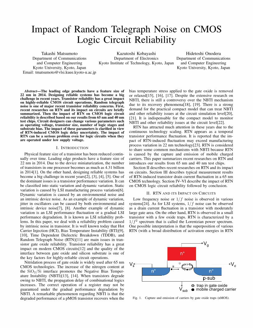
Fig. 2. RTN-induced drain current fluctuation in a pMOS.
switching trap in gate oxide
filled oxide trap in gate oxide
empty trap in gate oxide
EF : Fermi levelET : trap energy level
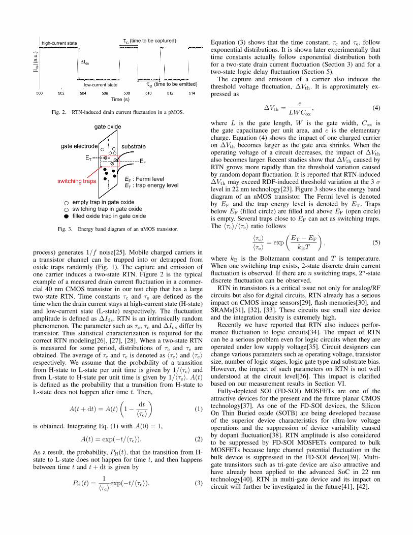
Fig. 3. Energy band diagram of an nMOS transistor.
process) generates 1/f noise[25]. Mobile charged carriers ina transistor channel can be trapped into or detrapped fromoxide traps randomly (Fig. 1). The capture and emission ofone carrier induces a two-state RTN. Figure 2 is the typicalexample of a measured drain current fluctuation in a commer-cial 40 nm CMOS transistor in our test chip that has a largetwo-state RTN. Time constants τc and τe are defined as thetime when the drain current stays at high-current state (H-state)and low-current state (L-state) respectively. The fluctuationamplitude is defined as ∆Ids. RTN is an intrinsically randomphenomenon. The parameter such as τc, τe and ∆Ids differ bytransistor. Thus statistical characterization is required for thecorrect RTN modeling[26], [27], [28]. When a two-state RTNis measured for some period, distributions of τc and τe areobtained. The average of τc and τe is denoted as ⟨τc⟩ and ⟨τe⟩respectively. We assume that the probability of a transitionfrom H-state to L-state per unit time is given by 1/⟨τc⟩ andfrom L-state to H-state per unit time is given by 1/⟨τe⟩. A(t)is defined as the probability that a transition from H-state toL-state does not happen after time t. Then,
A(t+ dt) = A(t)
(1− dt
⟨τc⟩
)(1)
is obtained. Integrating Eq. (1) with A(0) = 1,
A(t) = exp(−t/⟨τc⟩). (2)
As a result, the probability, PH(t), that the transition from H-state to L-state does not happen for time t, and then happensbetween time t and t+ dt is given by
PH(t) =1
⟨τc⟩exp(−t/⟨τc⟩). (3)
Equation (3) shows that the time constant, τc and τe, followexponential distributions. It is shown later experimentally thattime constants actually follow exponential distribution bothfor a two-state drain current fluctuation (Section 3) and for atwo-state logic delay fluctuation (Section 5).
The capture and emission of a carrier also induces thethreshold voltage fluctuation, ∆Vth. It is approximately ex-pressed as
∆Vth =e
LWCox, (4)
where L is the gate length, W is the gate width, Cox isthe gate capacitance per unit area, and e is the elementarycharge. Equation (4) shows the impact of one charged carrieron ∆Vth becomes larger as the gate area shrinks. When theoperating voltage of a circuit decreases, the impact of ∆Vth
also becomes larger. Recent studies show that ∆Vth caused byRTN grows more rapidly than the threshold variation causedby random dopant fluctuation. It is reported that RTN-induced∆Vth may exceed RDF-induced threshold variation at the 3 σlevel in 22 nm technology[23]. Figure 3 shows the energy banddiagram of an nMOS transistor. The Fermi level is denotedby EF and the trap energy level is denoted by ET. Trapsbelow EF (filled circle) are filled and above EF (open circle)is empty. Several traps close to EF can act as switching traps.The ⟨τc⟩/⟨τe⟩ ratio follows
⟨τc⟩⟨τe⟩
= exp
(ET − EF
kBT
), (5)
where kB is the Boltzmann constant and T is temperature.When one switching trap exists, 2-state discrete drain currentfluctuation is observed. If there are n switching traps, 2n-statediscrete fluctuation can be observed.
RTN in transistors is a critical issue not only for analog/RFcircuits but also for digital circuits. RTN already has a seriousimpact on CMOS image sensors[29], flash memories[30], andSRAMs[31], [32], [33]. These circuits use small size deviceand the integration density is extremely high.
Recently we have reported that RTN also induces perfor-mance fluctuation to logic circuits[34]. The impact of RTNcan be a serious problem even for logic circuits when they areoperated under low supply voltage[35]. Circuit designers canchange various parameters such as operating voltage, transistorsize, number of logic stages, logic gate type and substrate bias.However, the impact of such parameters on RTN is not wellunderstood at the circuit level[36]. This impact is clarifiedbased on our measurement results in Section VI.
Fully-depleted SOI (FD-SOI) MOSFETs are one of theattractive devices for the present and the future planar CMOStechnology[37]. As one of the FD-SOI devices, the SiliconOn Thin Buried oxide (SOTB) are being developed becauseof the superior device characteristics for ultra-low voltageoperations and the suppression of device variability causedby dopant fluctuation[38]. RTN amplitude is also consideredto be suppressed by FD-SOI MOSFETs compared to bulkMOSFETs because large channel potential fluctuation in thebulk device is suppressed in the FD-SOI device[39]. Multi-gate transistors such as tri-gate device are also attractive andhave already been applied to the advanced SoC in 22 nmtechnology[40]. RTN in multi-gate device and its impact oncircuit will further be investigated in the future[41], [42].
In the following section, the impact of RTN on CMOSlogic circuit reliability is described based on our measurementresults from 65 nm and 40 nm test chips.
III. TRANSISTOR DRAIN CURRENT FLUCTUATION BY RTN
This section describes typical measurement results of RTN-induced transistor drain current fluctuation with respect togate bias and substrate bias dependency. A CMOS transistorarray fabricated in a commercial 65 nm CMOS technologyis used. All measurements are done at room temperature.Figure 4 shows the RTN-induced nMOS drain current (Ids)fluctuation of a single transistor for various gate biases (Vgs).The current integration time is 5 ms for Vgs = 0.4V, 0.5V and500 µs for Vgs ≥ 0.6V. When Vgs is increased from 0.6 Vto 0.8 V, the two-state switching becomes more frequentlybut it disappears at 1.2 V. It indicates the gate bias gives abig influence on RTN. The power spectral density (PSD) ofFig. 4 is obtained by quantizing the measurement data intothe 2-state waveform. Lorentzian power spectrum is obtainedfor Vgs = 0.4V, 0.6V, 0.7V and 0.8V (Fig. 5). The largetwo-state switching disappears for Vgs = 1.2V and only a
Fig. 4. RTN-induced nMOS drain current fluctuation of one transistor forvarious gate biases.
Frequency (Hz)
PS
D (
a.u
.)
Vgs = 0.4V0.5V
0.6V
0.7V
0.8V
1.2V
1/f2
1/f2
10 1 100 101 102 103
Fig. 5. Power spectral density of Fig. 4.
high frequency noise with small amplitude remains. Lorentzianpower spectrum is not obtained for Vgs = 0.5V, because afrequent but a small two-state fluctuation and a large sharpfluctuation are superposed.
Figure 6 shows time constant (τc, τe) distributions of Fig. 5for Vgs = 0.8V. It is found that both distributions followexponential distribution (e−t/⟨τ⟩) and Eq. 3 is confirmed.Finally, Ids fluctuation for various substrate biases (Vsub) areshown in Fig. 7 at |Vgs| = 0.9V. The minus and plus signs inVsub represent reverse bias and forward bias respectively. Thelarge two-state RTN is observed for each Vsub. Ids stays atthe high-current state most of the time when the substrate isreverse-biased (Vsub:−0.4V), while it stays at the low-currentstate most of the time when the substrate is forward-biased(Vsub: +0.4V). Ids stays almost equally at both states for thezero substrate bias case (Vsub: 0V). It suggests that RTN timeconstants can be strongly influenced by the substrate bias.
From these measurement results, we are afraid that RTN-induced transistor current fluctuation can be strongly influ-enced by both the gate bias and the substrate bias.
Fig. 6. Time constant distribution of Fig. 4 (Vgs = 0.8 V).
: Reverse substrate bias
0 : No substrate bias
: Forward substrate bias
Fig. 7. RTN-induced pMOS drain current fluctuation of one transistor forvarious substrate biases.
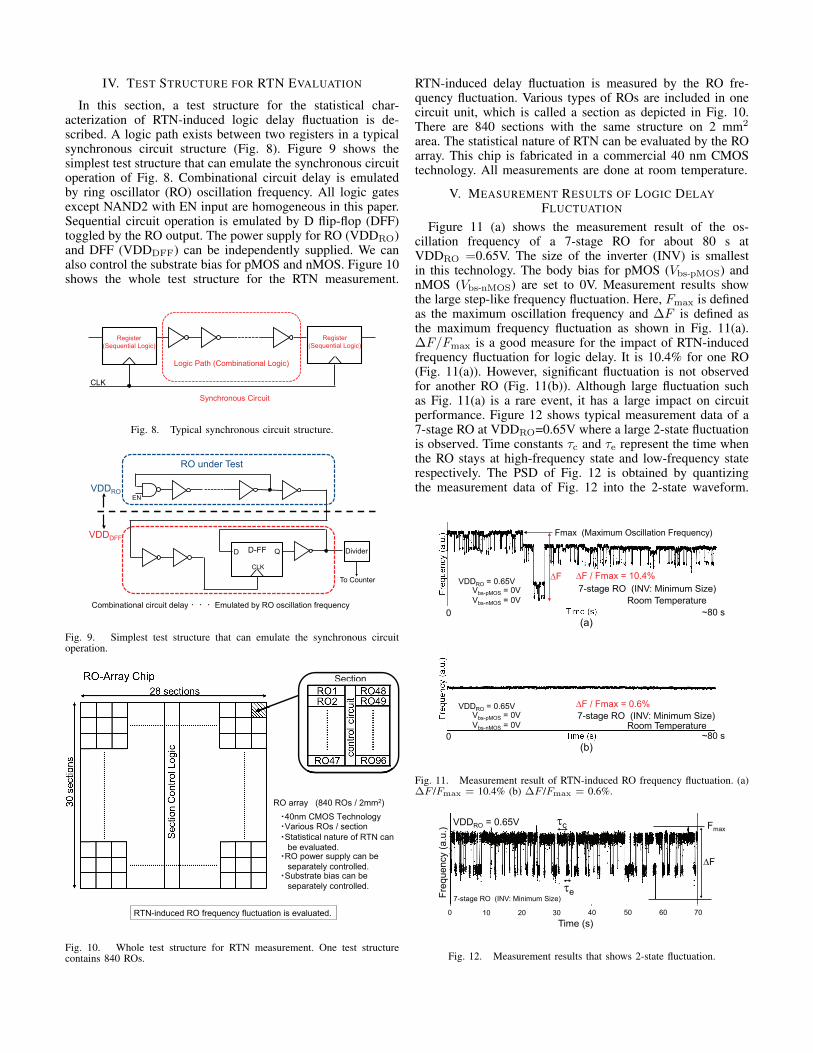
IV. TEST STRUCTURE FOR RTN EVALUATION
In this section, a test structure for the statistical char-acterization of RTN-induced logic delay fluctuation is de-scribed. A logic path exists between two registers in a typicalsynchronous circuit structure (Fig. 8). Figure 9 shows thesimplest test structure that can emulate the synchronous circuitoperation of Fig. 8. Combinational circuit delay is emulatedby ring oscillator (RO) oscillation frequency. All logic gatesexcept NAND2 with EN input are homogeneous in this paper.Sequential circuit operation is emulated by D flip-flop (DFF)toggled by the RO output. The power supply for RO (VDDRO)and DFF (VDDDFF) can be independently supplied. We canalso control the substrate bias for pMOS and nMOS. Figure 10shows the whole test structure for the RTN measurement.
CLK
Register
(Sequential Logic)
Register
(Sequential Logic)
Logic Path (Combinational Logic)
Synchronous Circuit
Fig. 8. Typical synchronous circuit structure.
Combinational circuit delay Emulated by RO oscillation frequency
CLK
EN
RO under Test
D Q Divider
To Counter
VDDRO
VDDDFF
D-FF
Fig. 9. Simplest test structure that can emulate the synchronous circuitoperation.
RO array (840 ROs / 2mm2)
Statistical nature of RTN can
be evaluated.RO power supply can be
separately controlled.
RTN-induced RO frequency fluctuation is evaluated.
40nm CMOS TechnologyVarious ROs / section
Substrate bias can be
separately controlled.
SectionSection
Fig. 10. Whole test structure for RTN measurement. One test structurecontains 840 ROs.
RTN-induced delay fluctuation is measured by the RO fre-quency fluctuation. Various types of ROs are included in onecircuit unit, which is called a section as depicted in Fig. 10.There are 840 sections with the same structure on 2 mm2
area. The statistical nature of RTN can be evaluated by the ROarray. This chip is fabricated in a commercial 40 nm CMOStechnology. All measurements are done at room temperature.
V. MEASUREMENT RESULTS OF LOGIC DELAYFLUCTUATION
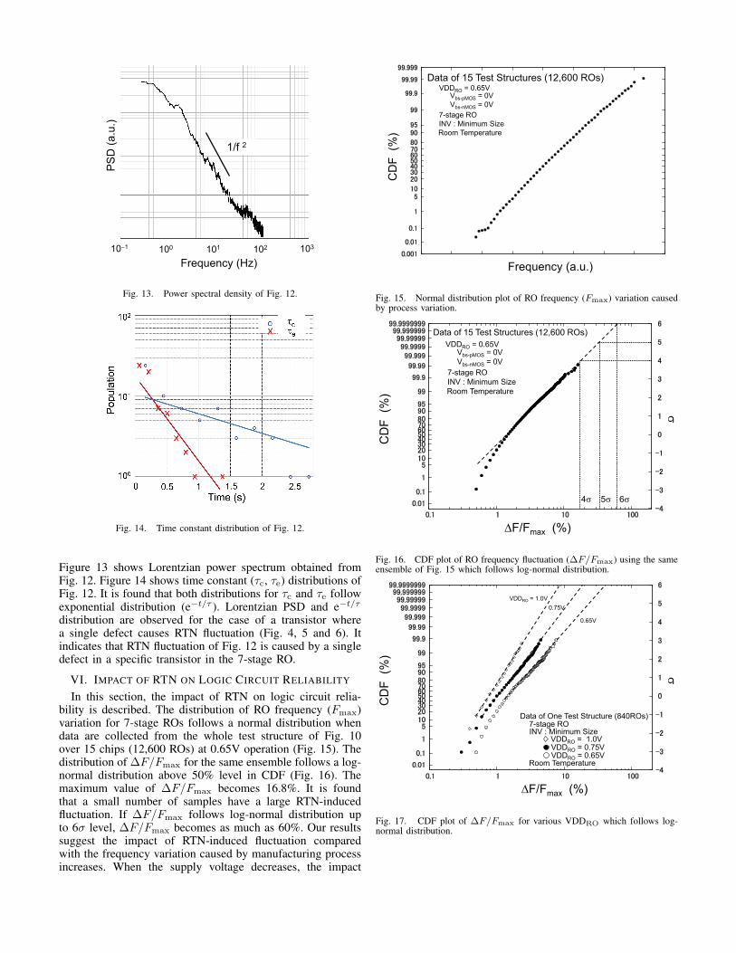
Figure 11 (a) shows the measurement result of the os-cillation frequency of a 7-stage RO for about 80 s atVDDRO =0.65V. The size of the inverter (INV) is smallestin this technology. The body bias for pMOS (Vbs-pMOS) andnMOS (Vbs-nMOS) are set to 0V. Measurement results showthe large step-like frequency fluctuation. Here, Fmax is definedas the maximum oscillation frequency and ∆F is defined asthe maximum frequency fluctuation as shown in Fig. 11(a).∆F/Fmax is a good measure for the impact of RTN-inducedfrequency fluctuation for logic delay. It is 10.4% for one RO(Fig. 11(a)). However, significant fluctuation is not observedfor another RO (Fig. 11(b)). Although large fluctuation suchas Fig. 11(a) is a rare event, it has a large impact on circuitperformance. Figure 12 shows typical measurement data of a7-stage RO at VDDRO=0.65V where a large 2-state fluctuationis observed. Time constants τc and τe represent the time whenthe RO stays at high-frequency state and low-frequency staterespectively. The PSD of Fig. 12 is obtained by quantizingthe measurement data of Fig. 12 into the 2-state waveform.
Fmax (Maximum Oscillation Frequency)
F
Vbs-pMOS = 0V
Vbs-nMOS = 0V
VDDRO = 0.65V
~80 s
F / Fmax = 10.4%
Room Temperature
(a)0
~80 s0
F / Fmax = 0.6%
Room Temperature
Vbs-pMOS = 0V
Vbs-nMOS = 0V
VDDRO = 0.65V
7-stage RO (INV: Minimum Size)
(b)
7-stage RO (INV: Minimum Size)
Fig. 11. Measurement result of RTN-induced RO frequency fluctuation. (a)∆F /Fmax = 10.4% (b) ∆F /Fmax = 0.6%.
c
e
Time (s)
Fre
quency (
a.u
.)
VDDRO = 0.65V Fmax
F
706050403020100
7-stage RO (INV: Minimum Size)
Fig. 12. Measurement results that shows 2-state fluctuation.
1/f 2
10 1 100 101 102 103
Frequency (Hz)
PS
D (
a.u
.)
10 1 100 101 102 103
Fig. 13. Power spectral density of Fig. 12.
Fig. 14. Time constant distribution of Fig. 12.
Figure 13 shows Lorentzian power spectrum obtained fromFig. 12. Figure 14 shows time constant (τc, τe) distributions ofFig. 12. It is found that both distributions for τc and τe followexponential distribution (e−t/τ ). Lorentzian PSD and e−t/τ
distribution are observed for the case of a transistor wherea single defect causes RTN fluctuation (Fig. 4, 5 and 6). Itindicates that RTN fluctuation of Fig. 12 is caused by a singledefect in a specific transistor in the 7-stage RO.
VI. IMPACT OF RTN ON LOGIC CIRCUIT RELIABILITY
In this section, the impact of RTN on logic circuit relia-bility is described. The distribution of RO frequency (Fmax)variation for 7-stage ROs follows a normal distribution whendata are collected from the whole test structure of Fig. 10over 15 chips (12,600 ROs) at 0.65V operation (Fig. 15). Thedistribution of ∆F/Fmax for the same ensemble follows a log-normal distribution above 50% level in CDF (Fig. 16). Themaximum value of ∆F/Fmax becomes 16.8%. It is foundthat a small number of samples have a large RTN-inducedfluctuation. If ∆F/Fmax follows log-normal distribution upto 6σ level, ∆F/Fmax becomes as much as 60%. Our resultssuggest the impact of RTN-induced fluctuation comparedwith the frequency variation caused by manufacturing processincreases. When the supply voltage decreases, the impact
Frequency (a.u.)
VDDRO = 0.65V Vbs-pMOS = 0V
Vbs-nMOS = 0V
Data of 15 Test Structures (12,600 ROs)
Room Temperature
7-stage RO
INV : Minimum Size
CD
F
(%)
Fig. 15. Normal distribution plot of RO frequency (Fmax) variation causedby process variation.
4 5 6
F/Fmax (%)
CD
F
(%)
VDDRO = 0.65V Vbs-pMOS = 0V
Vbs-nMOS = 0V
Data of 15 Test Structures (12,600 ROs)
Room Temperature
7-stage RO
INV : Minimum Size
Fig. 16. CDF plot of RO frequency fluctuation (∆F/Fmax) using the sameensemble of Fig. 15 which follows log-normal distribution.
0.65V
0.75V
VDDRO = 1.0V
F/Fmax (%)
CD
F
(%)
7-stage RO Data of One Test Structure (840ROs)
Room Temperature
VDDRO = 1.0VVDDRO = 0.75VVDDRO = 0.65V
INV : Minimum Size
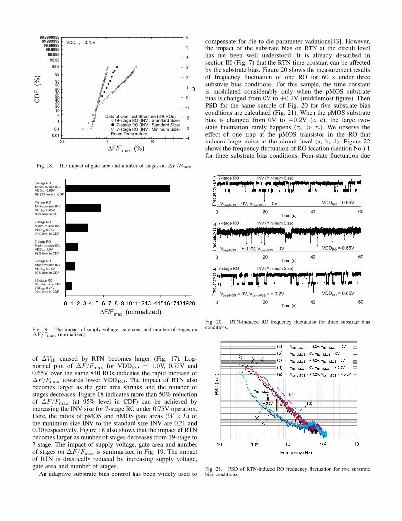
Fig. 17. CDF plot of ∆F/Fmax for various VDDRO which follows log-normal distribution.
VDDRO = 0.75V
7-stage RO (INV : Minimum Size)
Data of One Test Structure (840ROs)
CD
F
(%)
F/Fmax (%)
Room Temperature
7-stage RO (INV : Standard Size)19-stage RO (INV : Standard Size)
Fig. 18. The impact of gate area and number of stages on ∆F/Fmax.
19-stage RO
Standard size INV
VDDRO: 0.75V
99% level in CDF
F/Fmax (normalized)
7-stage RO
Standard size INV
VDDRO: 0.75V
99% level in CDF
7-stage RO
Minimum size INV
VDDRO: 1.0V
99% level in CDF
7-stage RO
Minimum size INV
VDDRO: 0.75V
99% level in CDF
7-stage RO
Minimum size INV
VDDRO: 0.65V
99% level in CDF
7-stage RO
Minimum size INV
VDDRO: 0.65V
99.99% level in CDF
Fig. 19. The impact of supply voltage, gate area, and number of stages on∆F/Fmax (normalized).
of ∆Vth caused by RTN becomes larger (Fig. 17). Log-normal plot of ∆F/Fmax for VDDRO = 1.0V, 0.75V and0.65V over the same 840 ROs indicates the rapid increase of∆F/Fmax towards lower VDDRO. The impact of RTN alsobecomes larger as the gate area shrinks and the number ofstages decreases. Figure 18 indicates more than 50% reductionof ∆F/Fmax (at 95% level in CDF) can be achieved byincreasing the INV size for 7-stage RO under 0.75V operation.Here, the ratios of pMOS and nMOS gate areas (W × L) ofthe minimum size INV to the standard size INV are 0.21 and0.30 respectively. Figure 18 also shows that the impact of RTNbecomes larger as number of stages decreases from 19-stage to7-stage. The impact of supply voltage, gate area and numberof stages on ∆F/Fmax is summarized in Fig. 19. The impactof RTN is drastically reduced by increasing supply voltage,gate area and number of stages.
An adaptive substrate bias control has been widely used to
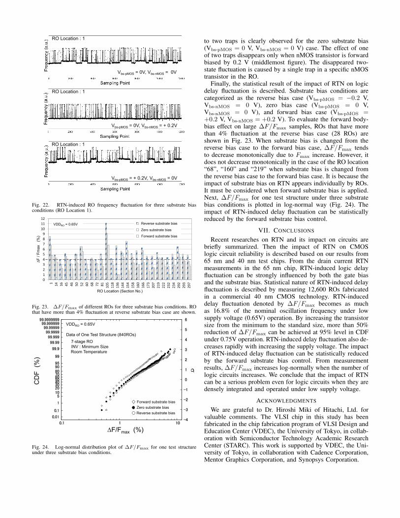
compensate for die-to-die parameter variations[43]. However,the impact of the substrate bias on RTN at the circuit levelhas not been well understood. It is already described insection III (Fig. 7) that the RTN time constant can be affectedby the substrate bias. Figure 20 shows the measurement resultsof frequency fluctuation of one RO for 60 s under threesubstrate bias conditions. For this sample, the time constantis modulated considerably only when the pMOS substratebias is changed from 0V to +0.2V (middlemost figure). ThenPSD for the same sample of Fig. 20 for five substrate biasconditions are calculated (Fig. 21). When the pMOS substratebias is changed from 0V to +0.2V (c, e), the large two-state fluctuation rarely happens (τc ≫ τe). We observe theeffect of one trap at the pMOS transistor in the RO thatinduces large noise at the circuit level (a, b, d). Figure 22shows the frequency fluctuation of RO location (section No.) 1for three substrate bias conditions. Four-state fluctuation due
Vbs-pMOS = 0V, Vbs-nMOS = 0V
Vbs-pMOS = + 0.2V, Vbs-nMOS = 0V
Vbs-pMOS = 0V, Vbs-nMOS = + 0.2V
VDDRO = 0.65V
VDDRO = 0.65V
VDDRO = 0.65V
7-stage RO INV (Minimum Size)
7-stage RO INV (Minimum Size)
7-stage RO INV (Minimum Size)
0 20 40 60
0 20 40 60
0 20 40 60
Fig. 20. RTN-induced RO frequency fluctuation for three substrate biasconditions.
Fig. 21. PSD of RTN-induced RO frequency fluctuation for five substratebias conditions.
Vbs-pMOS = 0V, Vbs-nMOS = 0V
RO Location : 1
Vbs-pMOS = 0V, Vbs-nMOS = + 0.2V
Vbs-pMOS = + 0.2V, Vbs-nMOS = 0V
RO Location : 1
RO Location : 1
Fig. 22. RTN-induced RO frequency fluctuation for three substrate biasconditions (RO Location 1).
0
1
2
3
4
5
6
7
8
9
10
11
12
1
14
16
45
46
50
52
60
68
72
81
105
118
136
144
154
158
160
166
173
207
219
222
232
234
292
293
297
F /
Fm
ax
(%
)
RO Location (Section No.)
1
2
3
VDDRO = 0.65V Reverse substrate bias
Zero substrate bias
Forward substrate bias
Fig. 23. ∆F/Fmax of different ROs for three substrate bias conditions. ROthat have more than 4% fluctuation at reverse substrate bias case are shown.
VDDRO = 0.65V
Data of One Test Structure (840ROs)
F/Fmax (%)
CD
F
(%)
Reverse substrate bias
Zero substrate bias
Forward substrate bias
Room Temperature
7-stage RO
INV : Minimum Size
Fig. 24. Log-normal distribution plot of ∆F/Fmax for one test structureunder three substrate bias conditions.
to two traps is clearly observed for the zero substrate bias(Vbs-pMOS = 0 V, Vbs-nMOS = 0 V) case. The effect of oneof two traps disappears only when nMOS transistor is forwardbiased by 0.2 V (middlemost figure). The disappeared two-state fluctuation is caused by a single trap in a specific nMOStransistor in the RO.
Finally, the statistical result of the impact of RTN on logicdelay fluctuation is described. Substrate bias conditions arecategorized as the reverse bias case (Vbs-pMOS = −0.2 V,Vbs-nMOS = 0 V), zero bias case (Vbs-pMOS = 0 V,Vbs-nMOS = 0 V), and forward bias case (Vbs-pMOS =+0.2 V, Vbs-nMOS = +0.2 V). To evaluate the forward body-bias effect on large ∆F/Fmax samples, ROs that have morethan 4% fluctuation at the reverse bias case (28 ROs) areshown in Fig. 23. When substrate bias is changed from thereverse bias case to the forward bias case, ∆F/Fmax tendsto decrease monotonically due to Fmax increase. However, itdoes not decrease monotonically in the case of the RO location“68”, “160” and “219” when substrate bias is changed fromthe reverse bias case to the forward bias case. It is because theimpact of substrate bias on RTN appears individually by ROs.It must be considered when forward substrate bias is applied.Next, ∆F/Fmax for one test structure under three substratebias conditions is plotted in log-normal way (Fig. 24). Theimpact of RTN-induced delay fluctuation can be statisticallyreduced by the forward substrate bias control.
VII. CONCLUSIONS
Recent researches on RTN and its impact on circuits arebriefly summarized. Then the impact of RTN on CMOSlogic circuit reliability is described based on our results from65 nm and 40 nm test chips. From the drain current RTNmeasurements in the 65 nm chip, RTN-induced logic delayfluctuation can be strongly influenced by both the gate biasand the substrate bias. Statistical nature of RTN-induced delayfluctuation is described by measuring 12,600 ROs fabricatedin a commercial 40 nm CMOS technology. RTN-induceddelay fluctuation denoted by ∆F/Fmax becomes as muchas 16.8% of the nominal oscillation frequency under lowsupply voltage (0.65V) operation. By increasing the transistorsize from the minimum to the standard size, more than 50%reduction of ∆F/Fmax can be achieved at 95% level in CDFunder 0.75V operation. RTN-induced delay fluctuation also de-creases rapidly with increasing the supply voltage. The impactof RTN-induced delay fluctuation can be statistically reducedby the forward substrate bias control. From measurementresults, ∆F/Fmax increases log-normally when the number oflogic circuits increases. We conclude that the impact of RTNcan be a serious problem even for logic circuits when they aredensely integrated and operated under low supply voltage.
ACKNOWLEDGMENTS
We are grateful to Dr. Hiroshi Miki of Hitachi, Ltd. forvaluable comments. The VLSI chip in this study has beenfabricated in the chip fabrication program of VLSI Design andEducation Center (VDEC), the University of Tokyo, in collab-oration with Semiconductor Technology Academic ResearchCenter (STARC). This work is supported by VDEC, the Uni-versity of Tokyo, in collaboration with Cadence Corporation,Mentor Graphics Corporation, and Synopsys Corporation.
REFERENCES
[1] S. Rusu, H. Muljono, D. Ayers, S. Tam, W. Chen, A. Martin, S. Li,S. Vora, R. Varada, and E. Wang, “Ivytown: A 22nm 15-core enterpriseXeon R⃝ processor family,” ISSCC Tech. Dig., p. 5.4, 2014.
[2] S. Borkar, “Designing reliable systems from unreliable components:The challenges of transistor variability and degradation,” IEEE Micro,vol. 25, p. 10, 2005.
[3] M. Alam, “Reliability- and process-variation aware design of integratedcircuits,” Microelectronics and Reliability, vol. 48, p. 1114, 2008.
[4] H. Onodera, “Variability modeling and impact on design,” IEDM Tech.Dig., p. 701, Dec. 2008.
[5] G. F. Taylor, “Where are we going? Product scaling in the system onchip era,” IEDM Tech. Dig., pp. 441–443, 2013.
[6] D. Boning and S. Nassif, “Models of process variations in device andinterconnect,” In Chapter 6 of “Design of High-Performance Micropro-cessor Circuits,” Edited by A. Chandrakasan, W. Bowhill, and F. Fox,pp. 98–115, IEEE Press, 2001.
[7] T. J. Yamaguchi, M. Soma, M. Ishida, T. Watanabe, and T. Ohmi,“Extraction of instantaneous and RMS sinusoidal jitter using an analyticsignal method,” IEEE Trans. Circuits and Systems II, vol. 50, pp. 288–298, Jun. 2003.
[8] M. P. Li, “Jitter challenges and reduction techniques at 10 Gb/s andbeyond,” IEEE Trans. Advanced Packaging, vol. 32, pp. 290–297, May2009.
[9] D. K. Schroder and J. A. Babcock, “Negative bias temperature instabil-ity: Road to cross in deep submicron silicon semiconductor manufac-turing,” J. App. Phys., vol. 94, no. 1, pp. 1–18, 2003.
[10] J. Stathis and S. Zafar, “The negative bias temperature instability in MOSdevices: A review,” Microelectronics and Reliability, vol. 46, no. 2-4,pp. 270–286, 2006.
[11] M. J. Kirton and M. J. Uren, “Noise in solid-state microstructures: Anew perspective on individual defects, interface states and low-frequency(1/f) noise,” Adv. Phys., vol. 38, no. 4, pp. 367–468, 1989.
[12] T. Nigam, “Impact of transistor level degradation on product reliability,”CICC Tech. Dig., pp. 431–438, 2009.
[13] N. Kimizuka, K. Yamaguchi, K. Imai, T. Iizuka, C. T. Liu, R. C. Keller,and T. Horiuchi, “NBTI enhancement by nitrogen incorporation intoultrathin gate oxide for 0.10µm gate CMOS generation,” Dig. Tech.Papers of Symp. on VLSI Tech., pp. 92–93, 2000.
[14] Y. Mitani, M. Nagamine, H. Satake, and A. Toriumi, “NBTI mechanismin ultra-thin gate dielectric –Nitrogen-originated mechanism in SiON–,”IEDM Tech. Dig., pp. 509–512, 2002.
[15] V. Huard, F. Monsieur, G. Ribes, and S. Bruyere, “Evidence forhydrogen-related defects during NBTI stress in p-MOSFETs,” Proc.IRPS, pp. 178–182, 2003.
[16] S. Tsujikawa, T. Mine, K. Watanabe, Y. Shimamoto, R. Tsuchiya,K. Ohnishi, T. Onai, J. Yugami, and S. Kimura, “Negative bias temper-ature instability of pMOSFETs woth ultra-thin SiON gate dielectrics,”Proc. IRPS, pp. 183–188, 2003.
[17] G. Chen, K. Y. Chuah, M. F. Li, D. S. Chan, C. H. Ang, J. Z. Zheng,Y. Jin, and D. L. Kwong, “Dynamic NBTI of PMOS transistors and itsimpact on device lifetime,” Proc. IRPS, pp. 196–202, 2003.
[18] S. Mahapatra, N. Goel, S. Desai, S. Gupta, B. Jose, S. Mukhopadhyay,K. Joshi, A. Jain, A. E. Islam, and M. A. Alam, “A comparative study ofdifferent physics-based NBTI models,” IEEE Trans. Electron Devices,vol. 60, pp. 901–916, Mar. 2013.
[19] T. Grasser, K. Rott, H. Reisinger, M. Waltl, P. Wagner, F. Schanovsky,W. Goes, G. Pobegen, and B. Kaczer, “Hydrogen-related volatile defectsas the possible cause for the recoverable component of NBTI,” IEDMTech. Dig., pp. 409–412, Dec. 2013.
[20] P. M. Lee, “Compact modeling for simulation of circuit reliability:Historical and industrial perspectives,” Proc. IRPS, pp. 2A.1.1–2A.1.6,2013.
[21] Y. Cao, J. Velamala, K. Sutaria, M. Chen, J. Ahlbin, I. Esqueda,M. Bajura, and M. Fritze, “Cross-layer modeling and simulation ofcircuit reliability,” IEEE Trans. CAD, vol. 33, pp. 8–23, Jan. 2014.
[22] T. Iizuka, J. Jeong, T. Nakura, M. Ikeda, and K. Asada, “All-digitalon-chip monitor for PMOS and NMOS process variability measurementutilizing buffer ring with pulse counter,” ESSCIRC Tech. Dig., pp. 182–185, 2010.
[23] N. Tega, H. Miki, Z. Ren, C. P. D’Emic, Y. Zhu, D. J. Frank, M. A.Guillorn, D.-G. Park, W. Haensch, and K. Torii, “Impact of HK/MGstacks and future device scaling on RTN,” Proc. IRPS, pp. 630–635,2011.
[24] P. Dutta and P. M. Horn, “Low-frequency fluctuations in solids: 1/fnoise,” Rev. Mod. Phys., vol. 53, no. 3, pp. 497–516, 1981.
[25] K. S. Ralls, W. J. Skocpol, L. D. Jackel, R. E. Howard, L. A. Fetter,R. W. Epworth, and D. M. Tennant, “Discrete resistance switching insubmicrometer silicon inversion layers: Individual interface traps andlow-frequency (1/f?) noise,” Phys. Rev. Lett., vol. 52, no. 3, pp. 228–231, 1984.
[26] K. Takeuchi, T. Nagumo, S. Yokogawa, K. Imai, and Y. Hayashi,“Single-charge-based modeling of transistor characteristics fluctuationsbased on statistical measurement of RTN amplitide,” Dig. Tech. Papersof Symp. on VLSI Tech., pp. 54–55, 2009.
[27] A. Teramoto, T. Fujisawa, K. Abe, S. Sugawa, and T. Ohmi, “Statisticalevaluation for trap energy level of RTS characteristics,” Dig. Tech.Papers of Symp. on VLSI Tech., pp. 99–100, 2010.
[28] H. Miki, N. Tega, M. Y. D. J. Frank, A. Bansal, M. Kobayashi, K. Cheng,C. P. D’Emic, Z. Ren, S. Wu, J.-B. Yau, Y. Zhu, M. A. Guillorn,D.-G. Park, W. Haensch, E. Leobandung, and K. Torii, “Statisticalmeasurement of random telegraph noise and its impact in scaled-downhigh-κ/metal-gate MOSFETs,” IEDM Tech. Dig., pp. 450–453, 2012.
[29] X. Wang, P. Rao, A. Mierop, and A. Theuwissen, “Random telegraphsignal in CMOS image sensor pixels,” IEDM Tech. Dig., pp. 115–118,2006.
[30] H. Kurata, K. Otsuga, A. Kotabe, S. Kajiyama, T. Osabe, Y. Sasago,S. Narumi, K. Tokami, S. Kamohara, and O. Tsuchiya, “Randomtelegraph signal in flash memory: Its impact on scaling of multilevel flashmemory beyond the 90-nm node,” IEEE J. Solid-State Circ., vol. 42,pp. 1362–1369, Jun. 2007.
[31] M. Yamaoka, H. Miki, A. Bansal, S. Wu, D. Frank, E. Leobandung, andK. Torii, “Evaluation methodology for random telegraph noise effectsin SRAM arrays,” IEDM Tech. Dig., pp. 745–748, 2011.
[32] K. Takeuchi, T. Nagumo, K. Takeda, A. Asayama, S. Yokogawa, K. Imai,and Y. Hayashi, “Direct observation of RTN-induced SRAM failure byaccelerated testing and its application to product reliability assessment,”Dig. Tech. Papers of Symp. on VLSI Tech., pp. 189–190, 2010.
[33] K. Takeuchi, T. Nagumo, and T. Hase, “Comprehensive SRAM designmethodology for RTN reliability,” Dig. Tech. Papers of Symp. on VLSITech., pp. 130–131, 2011.
[34] K. Ito, T. Matsumoto, S. Nishizawa, H. Sunagawa, K. Kobayashi, andH. Onodera, “The impact of RTN on performance fluctuation in CMOSlogic circuits,” Proc. IRPS, pp. 710–713, 2011.
[35] T. Matsumoto, K. Kobayashi, and H. Onodera, “Impact of randomtelegraph noise on CMOS logic delay uncertainty under low voltageoperation,” IEDM Tech. Dig., p. 581, Dec. 2012.
[36] T. Matsumoto, K. Kobayashi, and H. Onodera, “Impact of body-biasing technique on random telegraph noise induced delay fluctuation,”Japanese J. App. Phys., vol. 52, p. 04CE05, Apr. 2013.
[37] F. Arnaud, N. Planes, O.Weber, V. Barral, S. Haendler, P. Flatresse, andF. Nyer, “Switching energy efficiency optimization for advanced CPUthanks to UTBB technology,” IEDM Tech. Dig., pp. 48–51, 2012.
[38] H. Makiyama, Y. Yamamoto, H. Shinohara, T. Iwamatsu, H. Oda,N. Sugii, K. Ishibashi, T. Mizutani, T. Hiramoto, and Y. Yamaguchi,“Suppression of die-to-die delay variability of silicon on thin buriedoxide (SOTB) CMOS circuits by balanced P/N drivability control withback-bias for ultralow-voltage (0.4 V) operation,” IEDM Tech. Dig.,pp. 822–825, 2013.
[39] T. Hiramoto, A. Kumar, T. Mizutani, J. Nishimura, and T. Saraya,“Statistical advantages of intrinsic channel fully depleted SOI MOSFETsover bulk MOSFETs,” CICC Tech. Dig., p. 5.2, 2011.
[40] C.-H. Jan, U. Bhattacharya, R. Brain, S.-J. Choi, G. Curello, G. Gupta,W. Hafez, M. Jang, M. Kang, K. Komeyli, T. Leo, N. Nidhi, L. Pan,J. Park, K. Phoa, A. Rahman, C. Staus, H. Hashiro, C. Tsai, P. Van-dervoorn, L. Yang, J.-Y. Yeh, and P. Bai, “A 22 nm SoC platformtechnology featuring 3-D tri-gate and high-k/metalgate, optimized forultra low power, high performance and high density SoC applications,”IEDM Tech. Dig., pp. 44–47, 2012.
[41] Y. F. Lim, Y. Z. Xiong, N. Singh, R. Yang, Y. Jiang, D. S. H. Chan,W. Y. Loh, L. K. Bera, G. Q. Lo, N. Balasubramanian, and D.-L.Kwong, “Random telegraph signal noise in Gate-all-around Si-FinFETwith ultranarrow body,” IEEE Electron Device Lett., vol. 27, pp. 765–768, Sep. 2006.
[42] M.-L. Fan, V. P.-H. Hu, Y.-N. Chen, P. Su, and C.-T. Chuang, “Analysisof single-trap-induced random telegraph noise on FinFET devices, 6TSRAM cell, and logic circuits,” IEEE Trans. Electron Devices, vol. 59,pp. 2227–2234, Aug. 2012.
[43] J. W. Tschanz, J. T. Kao, S. G. Narendra, R. Nair, D. A. Antoniadis, A. P.Chandrakasan, and V. De, “Adaptive body bias for reducing impactsof Die-to-die and within-die parameter variations on microprocessorfrequency and leakage,” IEEE J. of Solid-State Circ., vol. 37, pp. 1396–1402, Nov. 2002.