
High Temperature SiC Electronics: Update and Outlook
26
National Aeronautics and Space Administration www.nasa.gov High Temperature SiC Electronics: Update and Outlook Glenn Beheim, Philip G. Neudeck, David J. Spry NASA Glenn Research Center http://www.grc.nasa.gov/WWW/SiC/ NASA Glenn Research Center Propulsion Controls and Diagnostics Workshop Cleveland, OH February 28-29, 2012
Transcript of High Temperature SiC Electronics: Update and Outlook

National Aeronautics and Space Administration
www.nasa.gov
High Temperature SiC Electronics: Update and Outlook
Glenn Beheim, Philip G. Neudeck, David J. Spry
NASA Glenn Research Center
http://www.grc.nasa.gov/WWW/SiC/
NASA Glenn Research Center Propulsion Controls and Diagnostics Workshop
Cleveland, OH February 28-29, 2012

National Aeronautics and Space Administration
www.nasa.gov 2
Efficient Power and Propulsion (EPP) Distributed Engine Control (DEC)
DEC Objectives: • Create a sustainable high temperature electronics infrastructure which will allow growth and integration of new control system technologies thus enabling a pathway to new engine technologies consistent with EPP goals.
• Create new tools which advance and help validate soft and hard control technologies which improve vehicle performance metrics and reduce specific energy consumption.
Silicon Carbide (SiC) Electronics Technology helps achieve these objectives by extending the operational limit of electronics to temperatures of 500 oC or more. This extends the capability of existing control hardware and enables entirely new control technologies to be applied in turbine engines. SiC Objectives: • Create the technologies for the high temperature electronics infrastructure to exist at an operational temperature range greater than 300 oC.

National Aeronautics and Space Administration
www.nasa.gov 3
Centralized control architecture with FADEC has been used since the mid 1980’s Distributed engine control features:
• Data concentrators • Smart sensors/actuators • Local loop closure • Digital I/O • Plug and play • Sensor bus • Reduced wire count and weight • Increased reliability • Expandability, flexibility, modularity
Implementation of distributed control inhibited by lack of high temperature electronics
• Active cooling of distributed modules is impractical • Catalog of 225 °C silicon-on-insulator (SOI) electronics needed initially • Use SiC for T > 300 °C
• Initially, hot-section applications, e.g., in-combustor smart pressure sensor • Longer term, expect higher temperatures more generally
• Increased power/weight engines • SiC power electronics for T < 300 °C
High Temperature Electronics: An Enabler for Distributed Engine Control

National Aeronautics and Space Administration
www.nasa.gov 4
600 °C SiC dynamic pressure sensor
CE-5 flame tube
Future sensor packages can incorporate 500 °C SiC
amplifier
High Temperature SiC Electronics Application: Amplified Dynamic Pressure Sensor for Active Combustion Control
600 °C SiC dynamic pressure sensor installed at station 3

National Aeronautics and Space Administration
www.nasa.gov
High Temperature Integrated Circuit Technology For T < 150 °C, bulk silicon MOSFET (CMOS) is basic building block of almost all (> 95%) integrated circuits in use today (computers, cell phones, etc.).
For T < 300 °C, well-developed Silicon-On-Insulator (SOI) IC’s available for low-power logic and signal processing functions.
Silicon Silicon
Bulk CMOS SOI CMOS
Above 300 °C ambient, wide bandgap semiconductors (SiC) are needed.
For power electronics: No SOI power electronics. SiC has significant advantages over Si at moderate to elevated temperatures (SiC particularly advantageous for T > 85 °C).
Many areas of sensing and control interest in jet engines are hotter than 300 °C.
5

National Aeronautics and Space Administration
www.nasa.gov
Power Applications Drive SiC Development
SiC power electronics cut cooling costs
At right: Cost breakdown for SiC Schottky Barrier Diodes (SBDs). Total = $1720/wafer; $0.94/part. Opportunity to move further down wafer/epitaxy cost curves!
6

National Aeronautics and Space Administration
www.nasa.gov 7
Pursuit of large power device market has funded development of many key technologies useful for SiC high temperature electronics (a niche market). Still a lot of high temperature specific technologies needed: • Ohmic contacts • Integrated circuit design • Insulators • Interconnects • Packaging
500 °C Durable Chip Packaging And Circuit Boards
(L.Y. Chen, 2002 GRC R&T Report) 500 °C Durable Metal-SiC Contacts (R. Okojie, 2000 GRC R&T Report)
100 um
SiC High Temperature Electronics Technologies

National Aeronautics and Space Administration
www.nasa.gov 8
SiC High Temperature Electronics Status Simple SiC integrated circuits have been demonstrated reliable at 500 °C. • Junction field effect transistor (JFET) technology
- avoids MOS oxide reliability issues, especially at high temperature - limits to integration because of power consumption (1 mW per gate)
• Digital and analog SiC ICs operated for 1000s of hrs at 500 °C. • Operation from -125 to +500 °C demonstrated. • Demonstrated devices have single interconnect level
<10 transistors and resistors per IC • ICs with >100 transistors have been designed
- Multilevel interconnects required • Multilevel interconnects demonstrated on small area
- Scaling up to 3 inch wafers
100 µm
Drain Gate
Source
200 µm
10 µ
m
200μm/10μm 6H-SiC JFET
0.0
0.2
0.4
0.6
0.8
1.0
0 10 20 30 40 50
100µm/10µm JFETT = 500 °C
Dra
in C
urre
nt (m
A)
Drain Voltage (V)
10000 hours
1 hour100 hours1000 hours
JFET Current vs. Voltage Characteristics

National Aeronautics and Space Administration
www.nasa.gov
- Metal-to-SiC contacts - High temperature packaging - SiC transistor (JFET) design
Digital NAND, NOR gates Analog differential amplifier
Multilevel Interconnect Structure: - Conformal metal layers - High temperature insulating layers
- Increase circuit density - Increase reliability and yield - Reduce crystalline defects
Transistors per IC
10
1000
100
2011 2012 2013 2015 2016 2014 2010 Development of High-Temperature SiC Integrated Circuits
∼ Apollo Guidance Computer levels of integration
(mid 1960’s)
Operational Amplifier A/D Converter Multiplexer
SiC Integrated Circuit Demonstrations: Microcontrollers
In-package amplifier for SiC dynamic pressure sensor (Supersonics/ERA)
Wireless capacitive pressure sensor for propulsion health monitoring (VSST)
Enabling Technologies for SiC Electronics:
Digital electronics for transmission of sensor signals on power cable (SFW)
500 °C demo
500 °C demo
500 °C demo
Venus seismometer (PIDDP)
500 °C demo
∼ First microprocessor levels of integration
(Intel 4004, released 1971)
9

National Aeronautics and Space Administration
www.nasa.gov
SiC Electronics Development at NASA Glenn
Funding Program
High Temperature SiC Electronics
Application Rationale Emphasis
VSST Wireless sensors for propulsion health monitoring
• Energy scavenging ---Fully wireless • Readily retrofit • First insertion of wireless---Safe
RF
SFW Distributed Engine Control
Smart sensors and actuators with digital I/O
Reduce cable count • Sensor bus • Data on power line • Close loop within actuator
Digital
Supersonics & ERA
In-package amplifier for SiC pressure sensor (for active combustion control)
High level output • Detect sub psi instabilities • Initiate control early • Reduced EMI susceptibility
Analog
Department of Energy
SiC crystal growth methods for reduced defect densities
Reduced defects for • Increased yield/reliability • Large area/high voltage devices
Power
10
National Aeronautics and Space Administration
www.nasa.gov
[1] R. S. Okojie, et al., J. Appl. Phys. 91, 6553 (2002). [2] L. Lipkin, et al. J. Electronic Materials 25, 909 (1996).
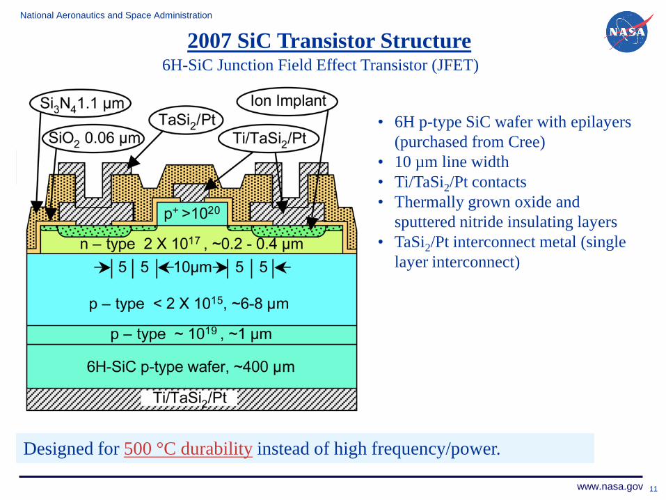
• 6H p-type SiC wafer with epilayers (purchased from Cree)
• 10 µm line width • Ti/TaSi2/Pt contacts • Thermally grown oxide and
sputtered nitride insulating layers • TaSi2/Pt interconnect metal (single
layer interconnect)
2007 SiC Transistor Structure 6H-SiC Junction Field Effect Transistor (JFET)
Designed for 500 °C durability instead of high frequency/power.
11
National Aeronautics and Space Administration
www.nasa.gov
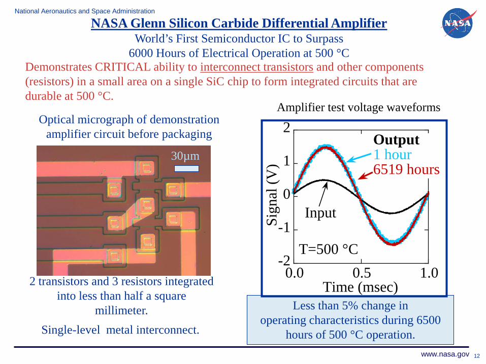
NASA Glenn Silicon Carbide Differential Amplifier World’s First Semiconductor IC to Surpass
6000 Hours of Electrical Operation at 500 °C Demonstrates CRITICAL ability to interconnect transistors and other components (resistors) in a small area on a single SiC chip to form integrated circuits that are durable at 500 °C.
Optical micrograph of demonstration amplifier circuit before packaging
Amplifier test voltage waveforms
2 transistors and 3 resistors integrated into less than half a square
millimeter. Less than 5% change in operating characteristics during 6500
hours of 500 °C operation. Single-level metal interconnect.
-2
-1
0
1
2
0.0 0.5 1.0Si
gnal
(V)
Time (msec)
Input
Output1 hour6519 hours
T=500 °C
30µm
12

National Aeronautics and Space Administration
www.nasa.gov
0 10 20 30
1 hour2405 hours
Time (msec)
- 5 V
- 5 V
- 5 V
0 V
-10 V
-10 V 0 V
-10 V0 V
OUT A+B
IN A
IN B
T = 500 °C
VHigh = -2.5, VLow = -7.5 V VDD = 20 V, VSS = -24 V
NASA Glenn SiC JFET NOR Gate IC
Waveforms of packaged NOR gate at 500 °C
OUT A+B
VDD
VSS GND
IN A IN B
Circuit Schematic
Probe-Test Photo
World’s First Semiconductor Digital IC to Surpass 2000 hours of 500 °C Operation
Digital chip failures between 2000 & 4000 hours - Higher supply voltages than analog circuits - Interconnect/insulator failure (?)
13

National Aeronautics and Space Administration
www.nasa.gov 14
1 cm
200μm/10μm 6H-SiC JFET
Differential Amplifier
Packaged Devices and Test Setup
Boards with chips reside in ovens.
Continuous electrical testing at 500 °C.
Wires to test instrumentation.
Oxidizing atmospheric air at 500 °C.
Parallel fabrication and testing of both single-transistors and IC’s

National Aeronautics and Space Administration
www.nasa.gov
100 µm Interconnects
(a) (b)
Wire Bond
As-fabricated chip After prolonged 500 °C test
500 °C circuit durability was limited by un-optimized dielectric & interconnect stack.
- Circuits failed after few thousand hours of 500 °C operation. - No discrete JFET failures observed through 10,000 hours @ 500 °C.
Present NASA GRC research is focusing on understanding interconnect failure and implementing revised multi-level interconnect process.
15

National Aeronautics and Space Administration
www.nasa.gov
Temperature Performance Issues
0.0
0.5
1.0
1.5
2.0
2.5
0 10 20 30 40 50
Dra
in C
urre
nt I D
(mA
)
Drain Voltage VD (V)
T = 25 °C
T = 500 °C
100µm/10µm JFET
Despite large (> 3X) change in JFET characteristics…
-10
-5
0
5
10
0.0 0.5 1.0 1.5 2.0
Sign
al (V
)Time (msec)
Output500 °C
Input(1V P-P)
Output25 °C
…nearly temperature-independent circuit operation can be achieved.
Inverting Amplifier Circuit
16

National Aeronautics and Space Administration
www.nasa.gov 17
0 1 2 3 4 5
Sign
al (V
)
Time (msec)
0
-5
-10
0
-5
-10
0
-5
-10
IN B
IN A
OUT
Sign
al (V
)
-124 °C+500 °C+20 °C
-10
-8
-6
-4
-2
0
0 1 2S
igna
l (V
)Time (msec)
+23 °C -125 °C -147 °C
Cold-Temperature Operation of SiC IC’s
NOR Gate Test Waveforms Ring Oscillator Test Waveforms “High Temperature” IC’s still function at cold temperatures down to -125 ° C!
Broadest temperature range ever reported for transistor IC’s. - NO change to circuit input voltages, output voltages change little. - Main performance change vs. temperature is circuit speed/frequency.

National Aeronautics and Space Administration
www.nasa.gov 18
Multilevel Interconnects to Enable Medium Scale Integration ICs
Next Generation ICs: • Circuits containing 10s to 100s of transistors,
resistors and capacitors
• 6 μm line width
• Three metal layers, each 1 µm thick - METAL1 Ohmic contact/interconnect - METAL2 Interconnect - METAL3 Bond pad
• Three SiO2 insulating layers, each 1 µm thick
• Si3N4 encapsulating layer
• 1:1 aspect ratios!
- Comparable to current Si IC technology! - But without surface planarization
(chemical mechanical polishing) - Thick oxide and metal layers needed - Refractory metals (TaSi2 used in all 3 layers)
- Low surface mobility—poor step coverage
Sputtered Film Step Coverage Top: On-axis sputtering Middle (L&R): Off-axis w/ rotation Bottom: Add heat, T→Tm

National Aeronautics and Space Administration
www.nasa.gov 19
Multilevel Interconnect Development
2010 Status: • TaSi2 deposited by off-axis sputtering w/ rotation for sidewall coverage.
• Patterning of TaSi2 films by wet etching resulted in undesired open circuits where METAL2 lines crossed
over METAL1 lines.
• Cross-sectional SEM showed a region of less dense METAL2 TaSi2 where it crosses over a step.
• The less dense TaSi2 etched at a much higher rate, resulting in high rates of removal from underneath the protective photoresist pattern. In many cases, the TaSi2 was completely removed, causing open circuits.
Optical micrograph showing undesired open circuits where METAL2 crosses METAL1.
Cross-sectional SEM showing reduced density METAL2 where it crosses a step.
Open circuits
METAL1
METAL2
SiO2
Void

National Aeronautics and Space Administration
www.nasa.gov 20
The following potential solutions for the metal patterning problems were investigated: • Reduce separation of sputter source and substrate to produce more uniformly dense TaSi2 films.
• Pattern METAL2 using plasma etching rather than wet etching (potentially less sensitive to TaSi2 density). Results: • Test structures were fabricated using newly developed TaSi2 deposition and etch processes.
• Inspection by cross-sectional SEM showed that the new processes eliminated unintentional open circuits.
• However, unintended short circuits were detected; these were determined to be caused by residual stringers
of METAL3 left on the surface, near step edges.
SiC circuit showing METAL2 crossing METAL1. Stringer defects (bright white in image) are residues of METAL3 (supposed to be fully removed here). Green line shows location of cross sectioning cut for SEM at right.
Pt coating for cross sectioning
SiO2
SiO2
SiO2
Metal1
Cross- sectional SEM showing excellent characteristics of metal lines crossing. Oxide and metal films are void free despite topography.
Stringer
Multilevel Interconnect Development
Metal2
Metal1
Metal2

National Aeronautics and Space Administration
www.nasa.gov 21
G D
S
0.E+00
5.E-04
1.E-03
0 10 20
Curr
ent
(A)
Voltage (V)
In order to remove the METAL3 stringers, a clean-up plasma etch was used (for future fabrication
runs stringer removal will be incorporated as part of the METAL3 etch). Testing at room temperature, using a probe station, has shown that many of the test devices (SiC transistors
and specialized multilevel interconnect test structures) operate as desired at room temperature.
Probe station testing of a SiC JFET, in which the current flow from drain (D) to source (S) is controlled by a voltage applied to the gate (G). Note that the gate interconnect (METAL2) crosses over the drain interconnect (METAL1).
Amplifying characteristics of the SiC JFET: Drain current is plotted vs. source-drain voltage, for gate voltages starting from 0 V (top trace) and incremented by -2V steps towards pinch off.
Room Temperature Demonstration of Multilevel Interconnect

National Aeronautics and Space Administration
www.nasa.gov 22
F G F
H
120 µm Optical micrograph of interlaced-fingers test structure. Eight upwards-pointing METAL1 fingers (i.e., pointing towards top of picture), connected to pad H, are interlaced with seven downwards-pointing METAL1 fingers, connected to pad G. The fingers are covered by a METAL2 plate electrode which is connected to the two F pads (all pads are METAL3). The fingers are insulated from each other and the overlying plate by a SiO2 dielectric layer.
Current-voltage (I-V) characteristics of fingers (H) to plate (F) capacitor, measured at 500 °C, after 1.5 hrs and 48 hrs of high temperature (400-500 °C) testing. The leakage of 0.15 µA at 50 V is acceptable for SiC microelectronics. The current peak at about 5 V (more pronounced after prolonged high temperature exposure) requires further investigation. It may be eliminated by the use of an encapsulating layer.
• An interlaced-finger-to-plate capacitive test structure requires the METAL2 layer (the plate) to cover a
corrugated surface and therefore provides a severe test of the interconnect process.
• This device, and other test structures, showed acceptably low levels of leakage during testing to 500 °C.
Demonstration of Interconnect at 500 °C

National Aeronautics and Space Administration
www.nasa.gov 23
Multilevel Interconnect Scale Up to 3 Inch Wafers
Current focus: Scale up close-range sputter deposition process for 3 inch wafers • Film densification by energetic particle bombardment • Sidewall coverage • Requires substrate rotation/translation for uniform film thickness
NASA designed close-range sputter deposition system
Close-range sputter deposition

National Aeronautics and Space Administration
www.nasa.gov 24
Circuit Inputs
Outputs Transistors, I/O Pads
Comments
4-Bit A/D Analog voltage signal, optional external clock, output type select
4 bit parallel digital latch, pulse width modulated (PWM)
203 JFETs, 23 I/Os Internal ring-oscillator clock circuit
2X2 Bit Static RAM Read, Write, Data Lines, Address Lines
4 bit parallel digital latch, pulse width modulated (PWM)
220 JFETs, 30 I/Os Address decoder, sense amplifiers
Source Separation Sensor Signal Transmitter
Capacitive sensor Frequency modulated with address code
301 JFETs, 20 I/Os Each sensor signal is tagged with unique address code
Ring Oscillators Capacitive sensors Frequency modulated signals (up to 500 MHz)
10-12 JFETs, 6 I/Os On-chip large transistors for power amplification
Binary Amplitude Modulation RF Transmitter
Low power binary signal
High-Power RF signal to antenna
Could connect with PWM from A/D
Op Amp, 2-Stage Differential Voltage gains to 50 w/ on-chip resistors
10 JFETs For piezoelectric SiC pressure sensors
4-Bit D/A 4 digital 1 analog 20 JFETs
SiC ICs to be Fabricated in Next Wafer Production Cycle

National Aeronautics and Space Administration
www.nasa.gov 25
Summary
• Simple SiC digital and analog integrated circuits have been demonstrated to be
reliable for 1000s of hours at 500 °C.
• Multilevel interconnect is key to developing more complex circuits with 10s to 100s of transistors.
• Multilevel interconnect process has been demonstrated on a small area.
• Process is being scaled up for 3 inch wafers.
• Other process issues are also being addressed, e.g., silicon nitride encapsulating layer to prevent contamination by salts.
• Processing improvements will enable fabrication of 3 inch SiC wafers with a wide range of high temperature integrated circuits suitable for distributed engine control applications.

National Aeronautics and Space Administration
www.nasa.gov 26
Acknowledgements
Work carried out by NASA Glenn Research Center
L. Evans, R. Okojie, R. Meredith, T. Ferrier,
M. Krasowski, N. Prokop NASA Glenn Research Center
C. Chang and D. Lukco ASRC Aerospace Corporation
L. Y. Chen Ohio Aerospace Institute
Technical Support Team K. Laster, J. Gonzalez, C. Blaha, R. Buttler, K. Moses, A. Miller