Heriot-Watt University · If you believe that this document breaches copyright please contact us...
27
Heriot-Watt University Research Gateway Heriot-Watt University Nanoelectromechanics of shuttle devices Shekhter, R. I.; Gorelik, L. Y.; Krive, I. V.; Kiselev, M. N.; Parafilo, A. V.; Jonson, Mats Published in: Nanoelectromechanical Systems DOI: 10.2478/nems-2013-0001 Publication date: 2013 Document Version Publisher's PDF, also known as Version of record Link to publication in Heriot-Watt University Research Portal Citation for published version (APA): Shekhter, R. I., Gorelik, L. Y., Krive, I. V., Kiselev, M. N., Parafilo, A. V., & Jonson, M. (2013). Nanoelectromechanics of shuttle devices. Nanoelectromechanical Systems, 1, 1-25. DOI: 10.2478/nems-2013- 0001 General rights Copyright and moral rights for the publications made accessible in the public portal are retained by the authors and/or other copyright owners and it is a condition of accessing publications that users recognise and abide by the legal requirements associated with these rights. If you believe that this document breaches copyright please contact us providing details, and we will remove access to the work immediately and investigate your claim.
Transcript of Heriot-Watt University · If you believe that this document breaches copyright please contact us...

Heriot-Watt University Research Gateway
Heriot-Watt University
Nanoelectromechanics of shuttle devicesShekhter, R. I.; Gorelik, L. Y.; Krive, I. V.; Kiselev, M. N.; Parafilo, A. V.; Jonson, Mats
Published in:Nanoelectromechanical Systems
DOI:10.2478/nems-2013-0001
Publication date:2013
Document VersionPublisher's PDF, also known as Version of record
Link to publication in Heriot-Watt University Research Portal
Citation for published version (APA):Shekhter, R. I., Gorelik, L. Y., Krive, I. V., Kiselev, M. N., Parafilo, A. V., & Jonson, M. (2013).Nanoelectromechanics of shuttle devices. Nanoelectromechanical Systems, 1, 1-25. DOI: 10.2478/nems-2013-0001
General rightsCopyright and moral rights for the publications made accessible in the public portal are retained by the authors and/or other copyright ownersand it is a condition of accessing publications that users recognise and abide by the legal requirements associated with these rights.
If you believe that this document breaches copyright please contact us providing details, and we will remove access to the work immediatelyand investigate your claim.

Download date: 05. Jul. 2018
Nanoelectromechanical SystemsResearch Article • DOI: 10.2478 nems-2013-0001 • NEMS • 2013 • 1-25
Nanoelectromechanics of shuttle devicesAbstractA single-electron tunneling (SET) device with a nanoscalecentral island that can move with respect to the bulk source-and drain electrodes allows for a nanoelectromechanical(NEM) coupling between the electrical current through the de-vice and the mechanical vibrations of the island. Althoughthe electromechanical “shuttle” instability and the associatedphenomenon of single-electron shuttling were predicted morethan 15 years ago, both theoretical and experimental studiesof NEM-SET structures are still carried out. New functionali-ties based on quantum coherence, Coulomb correlations andcoherent electron-spin dynamics are still of particular interest.In this article we present a short review of recent activities inthis area.
Keywords
PACS: 62.25.-g, 83.35.Gv, 74.20.Fg, 85.85.+j, 85.75.-d,72.10.Fk© Versita sp. z o.o.
R. I. Shekhter1, L. Y. Gorelik2, I. V. Krive3,4, M. N. Kiselev5,A. V. Parafilo3∗, M. Jonson1,6,7
1 Department of Physics, University of Gothenburg,SE-412 96 Göteborg, Sweden
2 Department of Applied Physics,Chalmers University of Technology, SE-412 96 Göteborg, Sweden
3 B. Verkin Institute for Low Temperature Physics and Engineeringof the National Academy of Sciences of Ukraine, 47 Lenin Ave.,Kharkov 61103, Ukraine
4 Physical Department, V. N. Karazin National University,Kharkov 61077, Ukraine
5 The Abdus Salam International Centre for Theoretical Physics,Strada Costiera 11, 1-34151 Trieste, Italy
6 SUPA, Institute of Photonics and Quantum Sciences,Heriot-Watt University, Edinburgh EH14 4AS, Scotland, UK
7 Department of Physics, Division of Quantum Phases and Devices,Konkuk University, Seoul 143-701, Korea
Received 17 December 2012Accepted 7 March 20131. Introduction
Electro-mechanical and mechano-electrical transductionphenomena have historically contributed greatly to theadvancement of technology in our society. Today, suchoperations can be achieved on the single-molecular levelwith obvious advantages brought about by the minia-turization of the devices involved. In addition, qualita-tively novel functionalities become available due to thenew physics that becomes relevant in materials struc-tured on the nanometer length scale. Quantum mechan-ics and electron-electron (Coulomb) correlations are thedefining ingredients of mesoscopic physics, which appliesto nanoscale devices whose properties may be determinedby a single or a few degrees of freedom. As a result, thereis an advantage in taking quantum coherence into accountwhen designing electro-mechanical devices for the pur-pose of quantum manipulation and quantum communica-tion.The single-electron tunneling (SET) transistor is a nano-device with particularly prominent mesoscopic features.Here, the Coulomb blockade of single-electron tunneling∗E-mail: [email protected]
at a low voltage bias and temperature [1] makes Ohm’s lawfor the electrical conductance invalid in the sense thatthe electrical current is not necessarily proportional tothe voltage drop across the device. Instead, the current isdue to a temporally discrete set of events where electronstunnel quantum-mechanically one-by-one from a source toa drain electrode via a nanometer sized island (a “quantumdot"). This is why the properties of a single electronicquantum state are crucial for the operation of the entiredevice.Since the probability for quantum mechanical tunneling isexponentially sensitive to the tunneling distance, it followsthat the position of the quantum dot relative to the elec-trodes is crucial. On the other hand, the strong Coulombforces that accompany the discrete nanoscale charge fluc-tuations, which are a necessary consequence of a currentflow through the SET device, might cause a significantdeformation of the device and move the dot, hence givingrise to a strong electro-mechanical coupling. This uniquefeature makes the so-called nanoelectromechanical SET(NEM-SET) devices, where mechanical deformation canbe achieved along with electronic operations, to be oneof the best nanoscale realizations of electromechanicaltransduction.Some of the latest achievements in the nano-electromechanics of NEM-SET devices focusing on the1
Brought to you by | Heriot-Watt UniversityAuthenticated | 137.195.59.30
Download Date | 1/29/14 2:11 PM

R. I. Shekhter, L. Y. Gorelik, I. V. Krive, M. N. Kiselev, A. V. Parafilo, M. Jonson
new functionality that exploits quantum coherence in boththe electronic and the mechanical subsystems will be dis-cussed. The choice of materials for making a NEM-SETdevice brings an additional dimension to exploring itsquantum performance. By choosing superconductors ormagnets as components of the device one may, for in-stance, take advantage of a macroscopic ordering of elec-trons with respect to both their charge and spin. The waysin which electric charge and spin contribute to electrome-chanical and mechanoelectrical transduction in a NEM-SET device will also be discussed. New effects also ap-pear due to the high mechanical deformability of molec-ular NEM-SET structures (polaronic effects) which couldbe accompanied with effects of strong electron-electroninteractions (Coulomb blockade and Luttinger liquid phe-nomena) as well as effects caused by strong tunnelingcoupling (Kondo nanomechanics).The phenomena of shuttling and the sensitivity of elec-tronic tunneling probabilities to mechanical deformationof the device are the focus of the present review. In thissense it is an update of our earlier reviews of shuttling [2–4]. Other aspects of nanoelectromechanics are only brieflydiscussed here. Readers are refered to the well-known re-views of Refs. 5–9 on nanoelectromechanical systems foradditional information.In Section 2, the basic concepts of electron shuttling (Sub-section 2.1) are introduced and the influence of polaroniceffects on the shuttle instability are considered (Subsec-tion 2.2). In the end of Subsection 2, the quantum shuttleis introduced and briefly discussed. Section 3 deals withthe shuttling of Cooper pairs (Subsection 3.1) and the po-laronic effects on the Josephson current through a vibrat-ing quantum dot (Subsection 3.2). A novel phenomenon— magnetic shuttling — is considered in Section 4, wherethe effects of spin-controlled shuttling of electric charge(Subsection 4.1), the spintro-mechanics of the magneticshuttle (Subsection 4.2) and mechanical transportation ofmagnetization (Subsection 4.3) are discussed. In the endof Section 3 the Kondo regime of electron shuttling isreviewed (Subsection 4.4). Recent experiments on theobservation of electron shuttling are briefly discussed inSection 5. Section 6 summarizes the latest theoreticalachievements in nanoelectromechanics of shuttle devices.2. Shuttling of single electronsA single-electron shuttle can be considered as the ulti-mate miniaturization of a classical electric pendulum ca-pable of transferring macroscopic amounts of charge be-tween two metal plates. In both cases the electric forceacting on a charged “ball" that is free to move in a poten-tial well between two metal electrodes kept at differentelectrochemical potentials, eV = µL − µR , results in self-
x
µ eVL =
µR = 0
LeadLead
Dot
Fig 1. Model system consisting of a movable quantum dot placed be-tween two leads. An effective elastic force acting on the dotdue to its connections to the leads is described by a parabolicpotential. Only one single electron state is available in the dotand the non-interacting electrons in the leads are assumed tohave a constant density of states. Reprinted with permissionfrom [12], D. Fedorets et al., Europhys. Lett. 58, 99 (2002). ©2002, EDP Sciences.
oscillations of the ball. Two distinct physical phenomena,namely the quantum mechanical tunneling mechanism forcharge loading (unloading) of the ball (in this case moreproperly referred to as a grain) and the Coulomb block-ade of tunneling, distinguish the nanoelectromechanicaldevice known as a single-electron shuttle [10] (see also[11]) from its classical textbook analog. The regime ofCoulomb blockade realized at bias voltages and temper-atures eV , T EC (where EC = e2/2C is the chargingenergy, C is the grain’s electrical capacitance) allows oneto consider single electron transport through the grain.Electron tunneling, being extremely sensitive to the po-sition of the grain relative to the bulk electrodes, leadsto a shuttle instability — the absence of any equilibriumposition of an initially neutral grain in the gap betweenthe electrodes.In Subsection 1 below we consider the characteristic fea-tures of the single-electron shuttle in the case whenthe shuttle dynamics can be treated as classical motion.Quantum corrections to this picture are then discussed inSubsection 2.2.1. Shuttle instability in the quantum regime ofCoulomb blockade
Theoretically, it is convenient to study the single-electronshuttle in an approach [12] where the grain is modeled asa single-level quantum dot (QD) that is weakly coupled(via a tunnel Hamiltonian) to the electrodes (see Fig. 1).The Hamiltonian corresponding to this model readsH = ∑
j=L,R H(j)l +HQD + ∑
j=L,R H(j)t , (1)
2Brought to you by | Heriot-Watt University
Authenticated | 137.195.59.30Download Date | 1/29/14 2:11 PM

Nanoelectromechanics of shuttle devices
where the HamiltonianH (j)l =∑
k
(εkj − µj )a†kjakj (2)describes noninteracting electrons in the left (j = L) andright (j = R ) leads, which are kept at different chemi-cal potentials µj ; a†kj (akj ) creates (annihilates) an electronwith momentum k in lead j . The QD Hamiltonian takesthe form
HQD = ε0d†d+ εiXd†d+ ~ω02 (X 2 + P2), (3)where d† (d) is the creation (destruction) operator for anelectron on the dot, ε0 is the energy of the resonant level,X is the dimensionless coordinate operator (normalized bythe amplitude x0 of zero-point fluctuations, x0 = √~/Mω0,M is the QD mass), P is the corresponding momentum op-erator ([X , P ] = i), ω0 is the frequency of vibrons and εiis the electromechanical interaction energy. The physicalmeaning of the second term in Eq. (3) is the interactionenergy due to the coupling of the electron charge den-sity on the dot with the electric potential φ(x) = Excm,where E = V /d0 is the electric field in the gap betweenelectrodes (d0 is the distance between the electrodes, xcmis the center-of-mass coordinate of the quantum dot). Inthis case the coupling "constant" εi from Eq. (3) is a linearfunction of bias voltage εi(V ) ' eV x0/d0.The tunneling Hamiltonian H (j)
t in Eq. (1) differs from itsstandard form. The explicit coordinate dependence of thetunneling matrix elements introduces additional electron-vibron interactions (additional to those described by thesecond term of Eq. (3). These result in the appearance ofquantum cohesive forces F (j)c = −∂H (j)
t /∂X , j = (+,−) ≡(L, R ), whereH (j)t =∑
k
t0j exp(jλtX )a†kjd+ h.c. (4)Here, t0j is the bare tunneling amplitude, which corre-sponds to a weak dot-electrode coupling, λt = x0/lt isa dimensionless parameter (lt is the electron tunnelinglength) that characterizes the sensitivity of the tunnelingmatrix elements to a shift of the dot center-of-mass coor-dinate with respect to its equilibrium (xcm = 0) position.The classical shuttle motion 〈X〉 = xc(t) 1 inducedby an applied voltage V is of particular interest in thisSection. Here the average 〈O〉 ≡ Trρ(t)O is takenwith the statistical operator ρ(t) obeying the Liouville-von Neumann equation
i~∂t ρ(t) = [H, ρ(t)]. (5)
0 10 20 30 40 50 600
0.05
0.1
0.15
eV, meV
I, n
A
Fig 2. Step-like I-V curves for single-electron shuttling for differentmodel parameters. Reprinted with permission from [12], D.Fedorets et al., Europhys. Lett. 58, 99 (2002). © 2002, EDPSciences.
For a weak electron-vibron interaction characterized bythe dimensionless coupling constant λ = −√2εi/~ω0 1, one can neglect the effects (∼ λ2) of zero-point QDfluctuations (see below). In this case, the classical dotcoordinate xc(t) is governed by Newton’s equation [12]xc + ω20xc = F (t)/M, (6)
where the average force F (t) = −Trρ(t)(∂H/∂X ) =Fe(t) + Fc(t) consists of two terms: the electric forceFe ∝ λ acting on the accumulated charge on the QD, andthe cohesive force, Fc ∝ λt , produced by the position-dependent hybridization of the electronic states of thegrain and the leads. The evaluation of both forces can bedone analytically [12, 13], either by solving the Heisen-berg equations of motion for the fermion operators (akj ,d) or by using the Keldysh Green’s function approach.The nonlinear Eq. (6) for the classical shuttle motion canbe analyzed in two cases: (i) near the shuttle instability(xc → 0), and (ii) for the developed shuttle motion (finitexc , small λtxc).For weak electromechanical coupling (λ, λt 1) it wasshown [12] that the amplitude of initially small oscilla-tions starts to grow exponentially (∼ erst) if eV > eVc =2(ε0+~ω0), which means that the threshold voltage for theshuttle instability is Vc . The rate of growth of the insta-bility, rs, depends on the level width Γ = ΓLΓR /(ΓL + ΓR ),where Γj = 2πν0|t0j |2 (ν0 is the density of states, whichis assumed to be an energy independent quantity in thewide band approximation [14, 15]) and on the strengths ofthe electromechanical coupling rs ∼ λλtΓ/~. It was alsoshown [12] that even in the absence of mechanical friction,which can be taken into account phenomenologically byadding to Eq. (6) the dissipative term γxc , the instabil-ity develops into a limit cycle. This is in contrast with a
3Brought to you by | Heriot-Watt University
Authenticated | 137.195.59.30Download Date | 1/29/14 2:11 PM
R. I. Shekhter, L. Y. Gorelik, I. V. Krive, M. N. Kiselev, A. V. Parafilo, M. Jonson
0.8
0.6
0.4
0.2
0
–0.22 4 6 8 10 12 14 16 18 20 22 24
eV/2
r(e
V/2
)/G
s
0wh
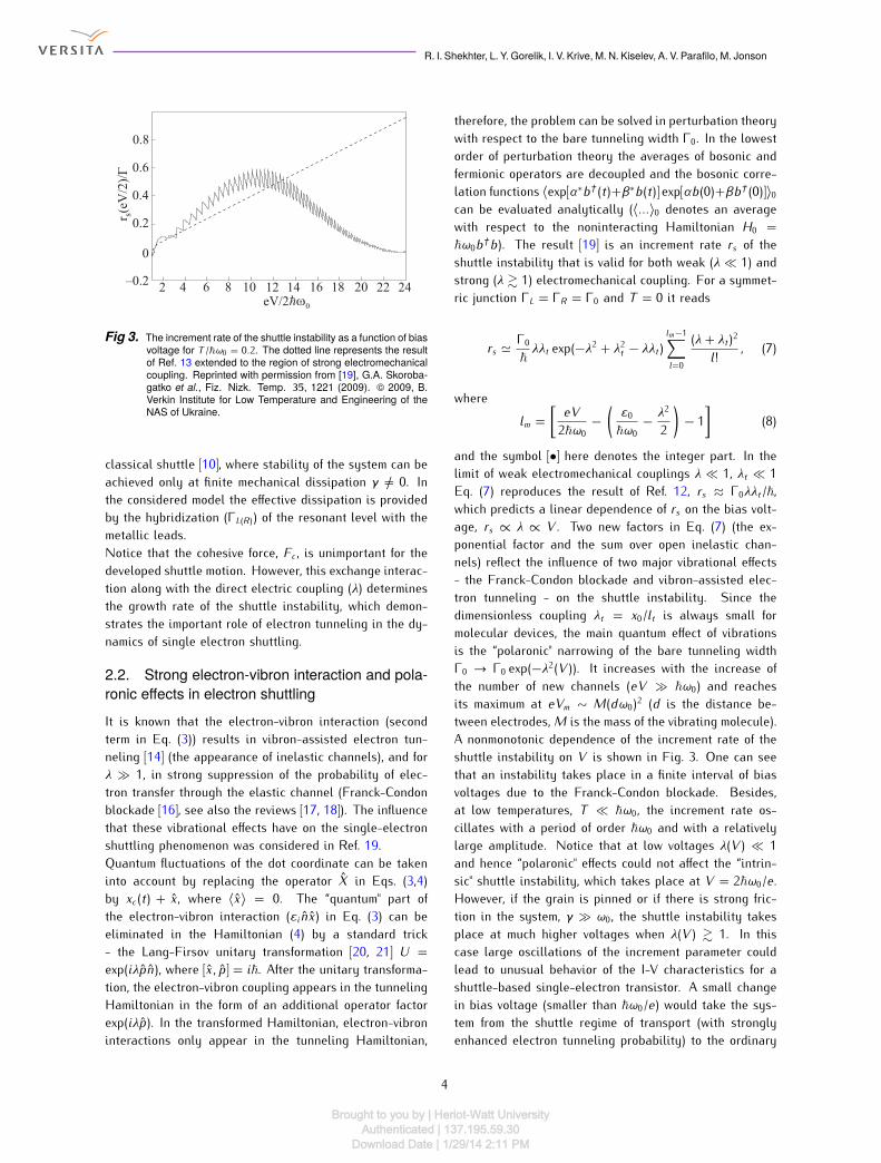
Fig 3. The increment rate of the shuttle instability as a function of biasvoltage for T /~ω0 = 0.2. The dotted line represents the resultof Ref. 13 extended to the region of strong electromechanicalcoupling. Reprinted with permission from [19], G.A. Skoroba-gatko et al., Fiz. Nizk. Temp. 35, 1221 (2009). © 2009, B.Verkin Institute for Low Temperature and Engineering of theNAS of Ukraine.
classical shuttle [10], where stability of the system can beachieved only at finite mechanical dissipation γ 6= 0. Inthe considered model the effective dissipation is providedby the hybridization (ΓL(R )) of the resonant level with themetallic leads.Notice that the cohesive force, Fc , is unimportant for thedeveloped shuttle motion. However, this exchange interac-tion along with the direct electric coupling (λ) determinesthe growth rate of the shuttle instability, which demon-strates the important role of electron tunneling in the dy-namics of single electron shuttling.2.2. Strong electron-vibron interaction and pola-ronic effects in electron shuttlingIt is known that the electron-vibron interaction (secondterm in Eq. (3)) results in vibron-assisted electron tun-neling [14] (the appearance of inelastic channels), and forλ 1, in strong suppression of the probability of elec-tron transfer through the elastic channel (Franck-Condonblockade [16], see also the reviews [17, 18]). The influencethat these vibrational effects have on the single-electronshuttling phenomenon was considered in Ref. 19.Quantum fluctuations of the dot coordinate can be takeninto account by replacing the operator X in Eqs. (3,4)by xc(t) + x , where 〈x〉 = 0. The “quantum" part ofthe electron-vibron interaction (εinx) in Eq. (3) can beeliminated in the Hamiltonian (4) by a standard trick- the Lang-Firsov unitary transformation [20, 21] U =exp(iλpn), where [x, p] = i~. After the unitary transforma-tion, the electron-vibron coupling appears in the tunnelingHamiltonian in the form of an additional operator factorexp(iλp). In the transformed Hamiltonian, electron-vibroninteractions only appear in the tunneling Hamiltonian,
therefore, the problem can be solved in perturbation theorywith respect to the bare tunneling width Γ0. In the lowestorder of perturbation theory the averages of bosonic andfermionic operators are decoupled and the bosonic corre-lation functions 〈exp[α∗b† (t)+β∗b(t)] exp[αb(0)+βb† (0)]〉0can be evaluated analytically (〈...〉0 denotes an averagewith respect to the noninteracting Hamiltonian H0 =~ω0b†b). The result [19] is an increment rate rs of theshuttle instability that is valid for both weak (λ 1) andstrong (λ & 1) electromechanical coupling. For a symmet-ric junction ΓL = ΓR = Γ0 and T = 0 it reads
rs 'Γ0~λλt exp(−λ2 + λ2
t − λλt) lm−1∑l=0
(λ+ λt)2l! , (7)
wherelm = [ eV2~ω0 −
(ε0~ω0 −
λ22)− 1] (8)
and the symbol [•] here denotes the integer part. In thelimit of weak electromechanical couplings λ 1, λt 1Eq. (7) reproduces the result of Ref. 12, rs ≈ Γ0λλt/~,which predicts a linear dependence of rs on the bias volt-age, rs ∝ λ ∝ V . Two new factors in Eq. (7) (the ex-ponential factor and the sum over open inelastic chan-nels) reflect the influence of two major vibrational effects- the Franck-Condon blockade and vibron-assisted elec-tron tunneling - on the shuttle instability. Since thedimensionless coupling λt = x0/lt is always small formolecular devices, the main quantum effect of vibrationsis the “polaronic" narrowing of the bare tunneling widthΓ0 → Γ0 exp(−λ2(V )). It increases with the increase ofthe number of new channels (eV ~ω0) and reachesits maximum at eVm ∼ M(dω0)2 (d is the distance be-tween electrodes, M is the mass of the vibrating molecule).A nonmonotonic dependence of the increment rate of theshuttle instability on V is shown in Fig. 3. One can seethat an instability takes place in a finite interval of biasvoltages due to the Franck-Condon blockade. Besides,at low temperatures, T ~ω0, the increment rate os-cillates with a period of order ~ω0 and with a relativelylarge amplitude. Notice that at low voltages λ(V ) 1and hence “polaronic" effects could not affect the “intrin-sic" shuttle instability, which takes place at V = 2~ω0/e.However, if the grain is pinned or if there is strong fric-tion in the system, γ ω0, the shuttle instability takesplace at much higher voltages when λ(V ) & 1. In thiscase large oscillations of the increment parameter couldlead to unusual behavior of the I-V characteristics for ashuttle-based single-electron transistor. A small changein bias voltage (smaller than ~ω0/e) would take the sys-tem from the shuttle regime of transport (with stronglyenhanced electron tunneling probability) to the ordinary4
Brought to you by | Heriot-Watt UniversityAuthenticated | 137.195.59.30
Download Date | 1/29/14 2:11 PM

Nanoelectromechanics of shuttle devices
regime of tunnel transport (small tunneling probability)and vice versa. Therefore one can expect pronounced neg-ative differential conductance (NDC) features (on the scaleof ~ω0/e) in the current voltage characteristics (see alsoRefs. 16, 22).It is interesting to note that in the absence of mechanicaldamping (γ = 0) the threshold voltage for single electronshuttling is determined by the vibron energy [12] eVth =2~ω0. This quantum threshold value indicates where theprocess of inelastic electron tunneling (with emission ofa vibron) becomes energetically available. In the realisticcase of finite friction, the threshold bias voltage is found bysolving the equation rs(Vth) = γ, where rs(V ) is defined inEq. (7) (see Fig. 3). In the limit of weak electromechanicalcoupling one gets for the threshold electric field (Eth =Vth/d), the result
eEth = ~γΓ Mω0lt , (9)has a linear dependence on the rate of dissipation γ. Theexponential increase (above threshold) of the amplitudeA(t) of the shuttle motion means that for the fully devel-oped (stationary) shuttle motion A(∞) x0. However, atthe initial stage of the instability the oscillation ampli-tude can be of the order of x0 and the classical treatmentof shuttle motion ceases to be valid.A fully quantum-mechanical approach to single electronshuttling was developed in Refs. 23–25, where it wasshown that the shuttle instability (exponential increaseof 〈x〉 and 〈p〉) in the limit lt lE = eE/Mω20 ∼ x0occurs for a threshold electric field that coincides withEq. (9), found in a quasiclassical approach. By using theWigner distribution function, which allows one to visualizethe behavior of a quantum system in phase space [24], twodifferent regimes of single electron shuttling were found.The classical regime (small fluctuations around the sta-tionary trajectory xc(t) = Ac sin(ω0t)) is realized for thefields E Eq > Eth, where [25]
eEq = C(x0lt
)4Mω20lt (10)
(C ' 10−2), i.e. in the case of weak mechanical dissipationγ . Γ(x0/lt)4 and for large bias voltages. For low biases,when the electric fields, acting on the charged QD are inthe interval Eth < E < Eq, the shuttle regime has a spe-cific quantum character. The Wigner function is stronglysmeared around the classical trajectory. It is concentratedin a region between two circles with radii Rout , Rin x0and Rout − Rin x0 for lt x0. This behavior is char-acterized by pronounced quantum fluctuations and can be
interpreted as a quantum shuttle. It is difficult to detect aquantum shuttle by measuring the average current sinceits qualitative behavior has no distinctive features in com-parison with the classical shuttle. The noise properties(and in general the full counting statistics) of NEMS willbe crucial for detecting single-electron shuttling.3. Mechanically mediated superconductivityand polaronic effects in the Josephson current
The shuttling of electric charges between nonsupercon-ducting electrodes by itself does not require phase co-herence. Even in the quantum regime of the Coulombblockade, when only a single (resonant) level is involvedin electron transport, phase coherent effects have littleinfluence on electron shuttling. This is not the case formagnetic and superconducting leads. Magnetic exchangeforces make the coherent electron-spin dynamics impor-tant for electron shuttling. Superconducting transportis, by definition, a phase coherent phenomenon and thusCooper-pair shuttling has to be significantly different fromsingle-electron shuttling.In this Section, the shuttling of Cooper pairs between twosuperconducting electrodes (Subsection 3.1) and the in-fluence of vibrational modes on the Josephson current areconsidered.3.1. Shuttling of Cooper pairs
The main requirement for the observation of a mechan-ically mediated Josephson current [26, 27] is that phasecoherence is preserved during the transportation of Cooperpairs between the two superconducting leads, and duringthe process of transferring charge between the bulk su-perconductors and a movable superconducting grain. Thisrequirement can be fulfilled if the superconducting grainis small enough to be in the Coulomb blockade regime [1](see also [28]) so that it can play the role of a single-Cooper-pair box [29] (see also [30, 31]). The implication isthat the characteristic energy scales of the small super-conducting grain – the Josephson energy EJ = (~2/2e)Jc(where Jc is the critical current) and the charging energyEC = (2e)2/2C (where C is the grain capacity) – haveto obey the double inequality EJ EC ∆0 (where∆0 is the superconducting gap) while the temperature hasto be low enough to make T EC . In this regime thesingle-electron states on the grain are energetically unfa-vorable (the parity effect [29, 32]) and the superconductingproperties of the system can be described by a two-levelmodel (see for example the review [33]). The correspond-ing state vector of a single-Cooper-pair box is a coherentsuperposition of the states with n = 0 and n = 1 ( moregenerally states with a different number of Cooper pairs:
5Brought to you by | Heriot-Watt University
Authenticated | 137.195.59.30Download Date | 1/29/14 2:11 PM

R. I. Shekhter, L. Y. Gorelik, I. V. Krive, M. N. Kiselev, A. V. Parafilo, M. Jonson
N and N + 1) on the grain. For a movable Cooper pairbox the energy scale for mechanical vibrations ~ω0 has tobe much smaller then all other energy scales. This addi-tional requirement prevents the creation of quasiparticlesand allows one to consider the mechanical motion of thegrain as an adiabatic process.The Hamiltonian of the system is expressed in terms ofthe Cooper pair number operator n for the grain and thephases of the superconducting leads, φL,R :H = −12 ∑
i=L,R EiJx(t)[eiφL,R |1〉〈0|+ h.c.] + δECx(t)n.
(11)The operator |1〉〈0| changes the number of Cooper pairson the grain. An essential feature here is the depen-dence of the charging energy difference δEC = EC (n =1) − EC (n = 0) and the coupling energies EL,RJ (x) =
E0 exp(−δxL,R /lt) (δxL,R is the distance between the grainand the respective lead) on the instantaneous position x(t)of the superconducting grain.It is useful to separate the adiabatic motion of the single-Cooper-pair box between the two superconducting elec-trodes into two different parts: (i) the free motion (trans-portation region in Fig. 4), and (ii) the process of loadingand unloading of charge near the leads (contact region inFig. 4). During the free motion, when the Josephson en-ergy is negligibly small and the Coulomb term dominates,the dynamics of the qubit is reduced to the time evolu-tion of the relative phase χ due to the second term inEq. (11), ~χ = δEC . In general, the accumulated phasesare different for left-to-right (t+) and right-to-left (t−) mo-tion; χ± ' δEC t±/~. The coherent exchange of a Cooperpair between the grain and the lead [stage (ii)] is charac-terized by the dimensionless Josephson coupling strength(θJ ' EJtc/~), where tc is the time spent by the grain incontact with the lead (see Fig. 4). The superconduct-ing phase difference φ = φR − φL, the dynamical phasesχ± and the Josephson coupling strength θJ fully controlthe behavior of the Josephson current. The characteristicvalue of the mechanically assisted supercurrent (the “criti-cal" current Jm) for a periodic motion of the grain (withfrequency f = ω0/2π) and for strong Josephson couplingθJ ≈ 1 is determined by the mechanical frequency only,Jm ' 2ef . An analytical expression for the mechanicallymediated dc Josephson current was derived in Ref. 26 andtakes the form
J = 2ef sin3 θJ cosθJ sin Φ(cosΦ + cosχ)1− (cos2 θJ cosχ − sin2 θJ cos Φ)2 , (12)where Φ = φ + χ+ − χ−, χ = χ+ + χ−. The currentEq. (12) is an oscillating function of the superconduct-ing phase difference φ (see Fig. 5), which is a spectac-ular manifestation of a Josephson coupling between the
Contact region Transportation region Contact region
Grain position
Energy
Accumulation of
relative phases
EJ
L
JE
R
EC
Josephson
tunneling
Josephson
tunneling
L R
t t
tt
1 2
40
Fig 4. Illustration of the charge transport process. The central islandmoves periodically between the leads. Close to each turningpoint Cooper pair tunneling between lead and island is pos-sible since the voltage on a gate electrode (not shown) hasbeen set to locally remove the electrostatic energy differencebetween having zero or one extra Cooper pair on the island(i.e., the difference in charging energy, δEC , is zero [34]). Asthe island retracts from the lead, tunneling is exponentially sup-pressed (EJ = 0) while the degeneracy of the two charge statesis lifted as the influence of the gate is weakened (δEC 6= 0)[26]. Reprinted with permission from [2], R. I. Shekhter et al.,J. Phys.: Condens. Matter 15, R441 (2003). © 2003, Instituteof Physics and IOP Publishing Limited.
remote superconductors. In the limit of weak couplingθJ 1 and vanishingly small dynamical phase (χ → 0)Eq. (12) is reduced to the standard Josephson formulaJ = Jc sinφ, where Jc ' eEJ /~. We see from Eq. (12) thatthe main qualitative effect of the dynamical phase, whichcan be controlled by the gate voltage, is a change of di-rection of the supercurrent (if cosχ + cosΦ < 0). For agiven strength of the Josephson coupling the direction ofa mechanically mediated supercurrent is determined bythe interplay of superconducting (φ) and dynamical (χ)phases. Notice that in Ref. 27 it was shown that mechani-cal transportation of Cooper pairs could establish relativephase coherence between two mesoscopic superconduc-tors if initially they are in states with strong uncorrelatedphase fluctuations.3.2. Josephson current through a vibrating quan-tum dot
In Section 2 we considered the influence of polaronic ef-fects on the electron shuttle instability. Here we analyzehow vibrational degrees of freedom affect the dc Josephsoncurrent. When studying the transport properties of a su-perconductor/quantum dot/superconductor (SQDS) junc-tion we will use the same simple model for the QD as inthe previous Section, i.e. we consider a dot with a singleenergy level ε0 that vibrates with angular frequency ω0and is weakly coupled to the superconducting leads. Thismodel is described by the standard BCS Hamiltonian withorder parameter ∆j = ∆0eiφj (∆0 is the superconductinggap and φj is the phase of the order parameter for the left,6
Brought to you by | Heriot-Watt UniversityAuthenticated | 137.195.59.30
Download Date | 1/29/14 2:11 PM

Nanoelectromechanics of shuttle devices
Fig 5. Magnitude of the current in Eq. (12) in units of 2ef as a functionof the phases Φ and χ . Regions of black correspond to no cur-rent and regions of white to J/2ef = 0.5. The direction of thecurrent, is indicated in by signs (±). To best see the “triangu-lar” structure of the current, the Josephson coupling has beenchosen to be θJ = π/3. Reprinted with permission from [2], R.I. Shekhter et al., J. Phys.: Condens. Matter 15, R441 (2003).© 2003, Institute of Physics and IOP Publishing Limited.
j = L, and right, j = R , superconductor). The coupling ofthe dot to the leads is described by a tunnel Hamiltonian,which introduces two energy scales to the problem, viz.the partial level widths ΓL,R . These are very significantfor the transport properties.The QD Hamiltonian readsHQD =∑
σε0d†σdσ +εin(b+b† )/√2+UC n↑n↓+~ω0b†b,(13)where dσ (d†σ ) is the destruction (creation) operator foran electron with spin projection σ =↑, ↓, n = n↑ + n↓,
nσ = d†σdσ , b(b† ) is the vibron destruction (creation) op-erator, εi is the electron-vibron interaction energy and UCis the electron-electron interaction energy. In what fol-lows we will assume that ∆0 is the largest energy scalein the problem. This allows one to neglect quasiparticles(continuum spectrum) when calculating the dc Josephsoncurrent.In general, a coupling to vibrational modes tends to sup-press the supercurrent [35, 36]. The suppression mecha-nism is different for “hard", ~ω0 Γ, and “soft", ~ω0 Γ,vibrons. For hard vibrons and for ~ω0 & ∆0 only theground state of the vibrational subsystem is involved inCooper pair transport through a S/QD/S junction. Zero-point fluctuations of the QD result in strong (exponential)renormalization of the electron tunneling probability (“po-laronic" narrowing of the level width). For strong electron-vibron coupling — i.e. for λ & 1, the critical current isexponentially suppressed [35], which is a manifestation of
the Franck-Condon blockade [16, 17] of the supercurrent.Notice that the Franck-Condon blockade will be partiallyremoved when ~ω0 ∆0 due to contributions of virtualside-band channels.The effect of the Franck-Condon blockade was first pre-dicted [35] for a nonresonant Josephson current J(φ) =J (λ)c sinφ, J (λ)c = exp(−2λ2)Jc (where Jc is the critical cur-rent in the absence of electron-vibron interaction, λ = 0).Later, in Ref. 37, it was demonstrated that in the caseUC = 0 and ∆0 →∞ an analogous result,
Jr(φ) = J (λ)r sin(φ/2)sgn[cos(φ/2)], (14)J (λ)r = (eΓ0
~
) exp(−λ2),holds also for the resonant (ε0 = 0,Γ0 = ΓL = ΓR ) cur-rent. Notice the extra factor of 2 in the exponent for thenonresonant critical current.The renormalization of the bare level width is hard to de-tect in an experiment (since one would have to vary thestrength of the electron-vibron interaction). Therefore, ex-permiental manifestations of Franck-Condon blocade mustbe analyzed. For normal transport, with an increase intemperature, the lifting of the blockade is accompanied bya nonmonotonic temperature behavior of the conductance[38, 39]. An analogous behavior has been predicted [40] forsuperconducting transport, where it is the critical currentthat reveals an anomalous T -dependence. The character-istic temperature which determines the peak in a plot ofJc(T ) vs. T is determined by the polaronic energy shiftEp ' ε2
i λω0. For T . Ep the critical current increaseswith temperature (in the regime of temperature-enhancedJosephson coupling) while for T Ep, the current scalesas 1/T due to a partial cancelation of Andreev levels con-tributions. For moderately strong electron-vibron inter-actions, λ & 1 the crossover from low-T regime to 1/T -scaling looks like a “resonant" enhancement of the criticalcurrent at T ∼ Ep (see Fig. 6).For soft vibrons, ω0 → 0, the slowly vibrating QD is al-ways able to change its equilibrium position (〈x〉 = 0)in order to minimize the total energy. If one neglectselectron-electron interactions (UC = 0) and if the dimen-sionless operator x = (b+ b† )/√2 in Eq. (13) is replacedby the classical variable xc , the total energy of the weaklink can be readily evaluated in the quasiclassical ap-proximation. The total energy, Et , then consists of twoterms: (i) the elastic energy, and (ii) the energy of thefilled Andreev levelEt = ~ω02 x2
c −√(ε0 + εixc)2 − Γ20 cos2(φ/2) (15)
(for simplicity we consider here a symmetric junction).It is easy to see that for coupling strengths such that7
Brought to you by | Heriot-Watt UniversityAuthenticated | 137.195.59.30
Download Date | 1/29/14 2:11 PM

R. I. Shekhter, L. Y. Gorelik, I. V. Krive, M. N. Kiselev, A. V. Parafilo, M. Jonson
0,0 0,1 0,2 0,3 0,4 0,5
0,08
0,10
0,12
0,14
0,16
J/J 0
0,2 0,3 0,4 0,50,020
0,022
0,024
0,026
0,028
T/Tp
Fig 6. Temperature dependence of the Josephson current for φ = 1,~ω0/εi = 0.25, the value of~ω0Γ0/ε2
i = 0.2 (inset -~ω0Γ0/ε2i =0.05). Reprinted with permission from [40], A. V. Parafilo et al.,
(unpublished).
ε2i ≥ ~ω0Γ0, a condition which is always fulfilled in theconsidered limit ω0 → 0, the energy minimum correspondsto a shifted QD position, xc 6= 0. In an effectively asym-metric junction the resonant (ε0 = 0) current is suppressed[40] so that
J(φ) = Jc sinφ , Jc = eω02(Γ0εi
)2. (16)
Unlike the exponential (in the electron-vibron interactionstrength) suppression of the critical current induced byzero-point fluctuations of the QD coordinate (~ω0 Γ0),soft vibrons give rise to a power-like (polaronic) suppres-sion of the form J ∝ λ−2. At finite temperatures thermallyexcited vibron polarons (excitations in the state xc 6= 0)tend to shift the QD towards its spatially symmetric po-sition. This means that |xc(T )| < |xc(0)|, which impliesthat at low temperatures the current increases with tem-perature. The crossover from the regime of a temperatureenhanced supercurrent to a standard 1/T scaling of thecritical current occurs abruptly at T ' Tp [40]. Therefore,both the Franck-Condon blockade of the supercurrent andthe polaronic effects on the Josephson current are man-ifested in an anomalous (nonmonotonic) temperature be-havior of the critical current (see Fig. 6). Estimationsshow [40] that for already existing transport experimentson suspended single wall carbon nanotubes, (see e.g. [41])the polaronic temperature is in the range Tp ∼ (1−10) K,which makes the observation of polaronic effects in carbonnanotube-based SNS junctions a feasible experiment.Finally, we discuss the influence of a charging energyUC on the polaronic effects on the Josephson current. Tothis end we first note that the electron-vibron interaction
renormalizes the electron-electron correlation energy sothat UC → UeffC = UC − 2λ2~ω0 and hence diminishes thestrength of the interaction [35]. It is physically obviousthat as long as Ueff
C . Γ the effects of a finite chargingenergy are negligible small. When UeffC > Γ correlationssplit the energy level ε0 and for Ueff
C Γ the conditionsfor resonant tunneling of Cooper pairs can not be satis-fied. If the electron-electron correlations are so strongthat UeffC ∆0, they additionally suppress the criticalcurrent by a factor Γ/∆0 1. If Ep Ueff
C . ∆0, thecharging energy changes the value of the low-T criticalcurrent but it can not influence the predicted anomaloustemperature dependence of the current at T ' Ep. How-ever, the question of happenes when UeffC ∼ Ep is stillopen.
4. Electro- and spintro-mechanics of mag-netic shuttle devicesIn this Section we will explore new functionalities thatemerge when nanomechanical devices are partly or com-pletely made of magnetic materials. The possibility ofmagnetic ordering brings new degrees of freedom into playin addition to the electronic and mechanical ones consid-ered so far, opening up an exciting perspective towardutilizing magneto-electro-mechanical transduction for alarge variety of applications. Device dimensions in thenanometer range mean that a number of mesoscopic phe-nomena in the electronic, magnetic and mechanical sub-systems can be used for quantum coherent manipulations.In comparison with the electromechanics of the nanode-vices considered above, the prominent role of the elec-tronic spin in addition to the electric charge should betaken into account.The ability to manipulate and control spins via electrical[42–44], magnetic [45] and optical [46] means has gen-erated numerous applications in metrology [47] in recentyears. A promising alternative method for spin manip-ulation employs a mechanical resonator coupled to themagnetic dipole moment of the spin(s), a method whichcould enable scalable quantum information architectures[48] and sensitive nanoscale magnetometry [49–51]. Mag-netic resonance force microscopy (MRFM) was suggestedas a means to improve spin detection to the level of asingle spin and thus enable three dimensional imaging ofmacromolecules with atomic resolution. In this techniquea single spin, driven by a resonant microwave magneticfield, interacts with a ferromagnetic particle. If the ferro-magnetic particle is attached to a cantilever tip, the spinchanges the cantilever vibration parameters [52]. The pos-sibility to detect [52] and monitor the coherent dynamicsof a single spin mechanically [53] has been demonstratedexperimentally. Several theoretical suggestions concern-
8Brought to you by | Heriot-Watt University
Authenticated | 137.195.59.30Download Date | 1/29/14 2:11 PM

Nanoelectromechanics of shuttle devices
ing the possibility to test single-spin dynamics throughan electronic transport measurement were made recently[54–57]. Complementary studies of the mechanics of a res-onator coupled to spin degrees of freedom by detecting thespin dynamics and relaxation were suggested in [54–61]and carried out in [62]. Electronic spin-orbit interactionin suspended nanowires was shown to be an efficient toolfor detection and cooling of bending-mode nanovibrationsas well as for manipulation of spin qubit and mechanicalquantum vibrations [63–65].An obvious modification of the nano-electro-mechanicsof magnetic shuttle devices originates from the spin-splitting of electronic energy levels, which results inthe known phenomenon of spin-dependent tunneling.Spin-controlled nano-electro-mechanics which originatesfrom spin-controlled transport of electric charge in mag-netic NEM systems is represented by a number of newmagneto-electro-mechanical phenomena.Qualitatively new opportunities appear when magneticnanomechanical devices are used. They have to do withthe effect of the short-ranged magnetic exchange interac-tion between the spin of electrons and magnetic parts ofthe device. In this case the spin of the electron ratherthan its electrical charge can be the main source of themechanical force acting on movable parts of the device.This leads to new physics compared with the usual elec-tromechanics of non-magnetic devices, for which we usethe term spintro-mechanics. In particular, it becomes pos-sible for a movable central island to shuttle magnetiza-tion between two magnetic leads even without any chargetransport between the leads. The result of such a mechan-ical transportation of magnetization is a magnetic couplingbetween nanomagnets with a strength and sign that aremechanically tunable.In this Section we will review some early results thatinvolve the phenomena mentioned above. These onlyamount to a first step in the exploration of new oppor-tunities caused by the interrelation between charge, spinand mechanics on a nanometer length scale.4.1. Spin-controlled shuttling of electric charge
By manipulating the interaction between the spin of elec-trons and external magnetic fields and/or the internal in-teraction in magnetic materials, spin-controlled nanoelec-tromechanics may be achieved.A new functional principle — spin-dependent shuttling ofelectrons — for low magnetic field sensing purposes wasproposed by Gorelik et al. in Ref. 66. This principle maylead to a giant magnetoresistance effect in external mag-netic fields as low as 1-10 Oe in a magnetic shuttle de-vice if magnets with highly spin-polarized electrons (halfmetals [67–71]) are used as leads in a magnetic shuttle
device. The key idea is to use the external magnetic fieldto manipulate the spin of shuttled electrons rather thanthe magnetization of the leads. Since the electron spendsa relatively long time on the shuttle, where it is decoupledfrom the magnetic environment, even a weak magnetic canrotate its spin by a significant angle. Such a rotation al-lows the spin of an electron that has been loaded ontothe shuttle from a spin-polarized source electrode to bereoriented in order to allow the electron finally to tunnelfrom the shuttle to the (differently) spin-polarized drainlead. In this way the shuttle serves as a very sensitive“magnetoresistor" device. The model employed in Ref. 66assumes that the source and drain are fully polarized inopposite directions. A mechanically movable quantum dot(described by a time-dependent displacement x(t)), wherea single energy level is available for electrons, performsdriven harmonic oscillations between the leads. The exter-nal magnetic field, H , is perpendicular to the orientationsof the magnetization in both leads and to the direction ofthe mechanical motion.The spin-dependent part of the Hamiltonian is specifiedasHmagn(t) = J(t)(a†↑a↑ −a†↓a↓)− gµH2 (a†↑a↓ +a†↓a↑), (17)
where J(t) = JR (t) − JL(t), JL(R )(t) are the exchange inter-actions between the on-grain electron and the left(right)lead, g is the gyromagnetic ratio and µ is the Bohr mag-neton. The proper Liouville-von Neumann equation forthe density matrix is analyzed and an average electricalcurrent is calculated for the case of large bias voltage.In the limit of weak exchange interaction, Jmax µH , onemay neglect the influence of the magnetic leads on theon-dot electron spin dynamics. The resulting current isI = eω0
πsin2(θ/2) tanh(w/4)sin2(θ/2) + tanh2(w/4) , (18)
where w is the total tunneling probability during the con-tact time t0, while θ ∼ πgµH/~ω0 is the rotation angleof the spin during the “free-motion" time.The theory [66] predicts oscillations in the magnetoresis-tance of the magnetic shuttle device with a period ∆Hp,which is determined from the equation ~ω0 = gµ(1 +w)∆Hp. The physical meaning of this relation is sim-ple: every time when ω0/Ω = n+ 1/2 (Ω = gµH/~ is thespin precession frequency in a magnetic field) the shut-tled electron is able to flip fully its spin to remove the“spin-blockade" of tunneling between spin polarized leadshaving their magnetization in opposite directions. This ef-fect can be used for measuring the mechanical frequency
9Brought to you by | Heriot-Watt University
Authenticated | 137.195.59.30Download Date | 1/29/14 2:11 PM

R. I. Shekhter, L. Y. Gorelik, I. V. Krive, M. N. Kiselev, A. V. Parafilo, M. Jonson
thus providing dc spectroscopy of nanomechanical vibra-tions.Spin-dependent shuttling of electrons as discussed aboveis a property of non-interacting electrons, in the sense thattunneling of different electrons into (and out of) the dot areindependent events. The Coulomb blockade phenomenonadds a strong correlation of tunneling events, preventingfluctuations in the occupation of electronic states on thedot. This effect crucially changes the physics of spin-dependent tunneling in a magnetic NEM device. One ofthe remarkable consequences is the Coulomb promotionof spin-dependent tunneling predicted in Ref. 72. In thiswork a strong voltage dependence of the spin-flip relax-ation rate on a quantum dot was demonstrated. Such re-laxation, being very sensitive to the occupation of spin-upand spin-down states on the dot, can be controlled by theCoulomb blockade phenomenon. It was shown in Ref. 72that by lifting the Coulomb blockade one stimulates oc-cupation of both spin-up and spin-down states thus sup-pressing spin-flip relaxation on the dot. In magnetic de-vices with highly spin-polarized electrons, electronic spin-flip can be the only mechanism providing charge transportbetween oppositely magnetized leads. In this case theonset of Coulomb blockade, by increasing the spin-flip re-laxation rate, stimulates charge transport through a mag-netic SET device (Coulomb promotion of spin-dependenttunneling). Spin-flip relaxation also qualitatively mod-ifies the noise characteristics of spin-dependent single-electron transport. In Refs. 73, 74 it was shown that thelow-frequency shot noise in such structures diverges asthe spin relaxation rate goes to zero. This effect pro-vides an efficient tool for spectroscopy of extremely slowspin-flip relaxation in quantum dots. Mechanical trans-portation of a spin-polarized dot in a magnetic shuttledevice provides new opportunities for studying spin-fliprelaxation in quantum dots. The reason can be traced toa spin-blockade of the mechanically aided shuttle currentthat occurs in devices with highly polarized and colin-early magnetized leads. As was shown in Ref. 75 theabove effect results in giant peaks in the shot-noise spec-tral function, wherein the peak heights are only limited bythe rates of electronic spin flips. This enables a nanome-chanical spectroscopy of rare spin-flip events, allowingspin-flip relaxation times as long as 10 µs to be detected.The spin-dependence of electronic tunneling in magneticNEM devices permits an external magnetic field to beused for manipulating not only electric transport but alsothe mechanical performance of the device. This wasdemonstrated in Refs. 76, 77. A theory of the quantum co-herent dynamics of mechanical vibrations, electron chargeand spin was formulated and the possibility to trigger ashuttle instability by a relatively weak magnetic field was
demonstrated. It was shown that the strength of the mag-netic field required to control nanomechanical vibrationsdecreases with an increasing tunnel resistance of the de-vice and can be as low as 10 Oe for giga-ohm tunnelstructures.A new type of nanoelectromechanical self excitationcaused entirely by the spin splitting of electronic en-ergy levels in an external magnetic field was predictedin Ref. 78 for a suspended nanowire, where mechanicalmotion in a magnetic field induces an electromotive cou-pling between electronic and vibrational degrees of free-dom. It was shown that a strong correlation betweenthe occupancy of the spin-split electronic energy levelsin the nanowire and the velocity of flexural nanowire vi-brations provides energy supply from the source of dc cur-rent, flowing through the wire, to the mechanical vibrationsthus making possible stable, self-supporting bending vi-brations. Estimations made in Ref. 78 show that in a re-alistic case the vibration amplitude of a suspended carbonnanotube (CNT) of the order of 10 nm can be achieved ifa magnetic field of 10 T is applied.4.2. Spintro-mechanics of magnetic shuttle de-vice
New phenomena, qualitatively different from the elec-tromechanics of nonmagnetic shuttle systems, may appearin magnetic shuttle devices in a situation when short-range magnetic exchange forces become comparable instrength to the long-range electrostatic forces betweenthe charged elements of the device [78]. There is convinc-ing evidence that the exchange field can be several teslaat a distance of a few nanometers from the surface of aferromagnet [79–82]. Because of the exponential decay ofthe field, the force experienced by a single-electron spinin the vicinity of magnetic electrodes can be very large.These spin-dependent exchange forces can lead to various“spintro-mechanical" phenomena.Mechanical effects produced by a long-range electro-static force and short-ranged exchange forces on a mov-able quantum dot are illustrated in Fig. 7. The electro-static force acting on the dot, placed in the vicinity of acharged electrode (Fig. 7(a)), is determined by the electriccharge accumulated on the dot. In contrast, the exchangeforce induced by a neighboring magnet depends on thenet spin accumulated on the dot. While the electrostaticforce changes its direction if the electric charge on thedot changes its sign, the spin-dependent exchange forceis insensitive to the electric charge but changes direc-tion if the electronic spin projection changes its sign. Avery important difference between the two forces is thatthe electrostatic force changes only as a result of injec-tion of additional electrons into (out of) the dot while the10
Brought to you by | Heriot-Watt UniversityAuthenticated | 137.195.59.30
Download Date | 1/29/14 2:11 PM
Nanoelectromechanics of shuttle devices
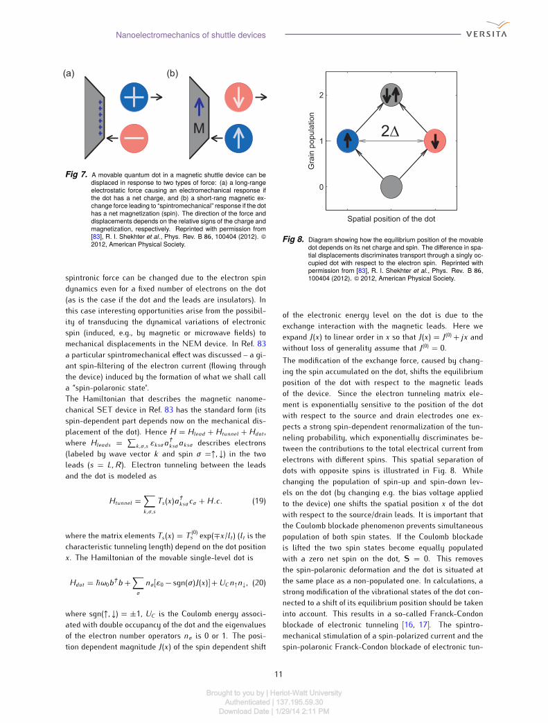
(a)
M
(b)
Fig 7. A movable quantum dot in a magnetic shuttle device can bedisplaced in response to two types of force: (a) a long-rangeelectrostatic force causing an electromechanical response ifthe dot has a net charge, and (b) a short-rang magnetic ex-change force leading to “spintromechanical” response if the dothas a net magnetization (spin). The direction of the force anddisplacements depends on the relative signs of the charge andmagnetization, respectively. Reprinted with permission from[83], R. I. Shekhter et al., Phys. Rev. B 86, 100404 (2012). ©2012, American Physical Society.
spintronic force can be changed due to the electron spindynamics even for a fixed number of electrons on the dot(as is the case if the dot and the leads are insulators). Inthis case interesting opportunities arise from the possibil-ity of transducing the dynamical variations of electronicspin (induced, e.g., by magnetic or microwave fields) tomechanical displacements in the NEM device. In Ref. 83a particular spintromechanical effect was discussed – a gi-ant spin-filtering of the electron current (flowing throughthe device) induced by the formation of what we shall calla “spin-polaronic state".The Hamiltonian that describes the magnetic nanome-chanical SET device in Ref. 83 has the standard form (itsspin-dependent part depends now on the mechanical dis-placement of the dot). Hence H = Hlead +Htunnel +Hdot ,where Hleads = ∑k,σ ,s εksσa
†ksσaksσ describes electrons(labeled by wave vector k and spin σ =↑, ↓) in the twoleads (s = L, R ). Electron tunneling between the leadsand the dot is modeled as
Htunnel = ∑k,σ ,s
Ts(x)a†ksσcσ +H.c. (19)where the matrix elements Ts(x) = T (0)
s exp(∓x/lt) (lt is thecharacteristic tunneling length) depend on the dot positionx . The Hamiltonian of the movable single-level dot isHdot = ~ω0b†b+∑
σnσ [ε0− sgn(σ )J(x)] +UCn↑n↓, (20)
where sgn(↑, ↓) = ±1, UC is the Coulomb energy associ-ated with double occupancy of the dot and the eigenvaluesof the electron number operators nσ is 0 or 1. The posi-tion dependent magnitude J(x) of the spin dependent shift
0
1
2
Spatial position of the dot
Gra
in p
opula
tion
2D
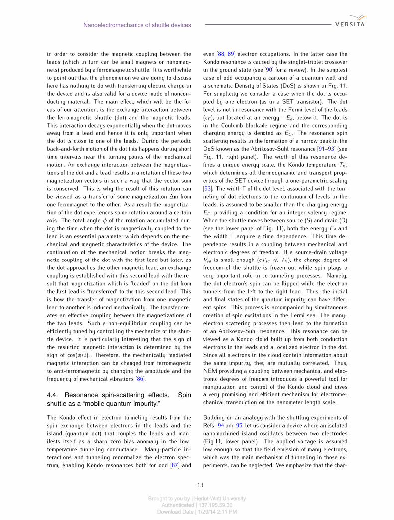
Fig 8. Diagram showing how the equilibrium position of the movabledot depends on its net charge and spin. The difference in spa-tial displacements discriminates transport through a singly oc-cupied dot with respect to the electron spin. Reprinted withpermission from [83], R. I. Shekhter et al., Phys. Rev. B 86,100404 (2012). © 2012, American Physical Society.
of the electronic energy level on the dot is due to theexchange interaction with the magnetic leads. Here weexpand J(x) to linear order in x so that J(x) = J (0) + jx andwithout loss of generality assume that J (0) = 0.The modification of the exchange force, caused by chang-ing the spin accumulated on the dot, shifts the equilibriumposition of the dot with respect to the magnetic leadsof the device. Since the electron tunneling matrix ele-ment is exponentially sensitive to the position of the dotwith respect to the source and drain electrodes one ex-pects a strong spin-dependent renormalization of the tun-neling probability, which exponentially discriminates be-tween the contributions to the total electrical current fromelectrons with different spins. This spatial separation ofdots with opposite spins is illustrated in Fig. 8. Whilechanging the population of spin-up and spin-down lev-els on the dot (by changing e.g. the bias voltage appliedto the device) one shifts the spatial position x of the dotwith respect to the source/drain leads. It is important thatthe Coulomb blockade phenomenon prevents simultaneouspopulation of both spin states. If the Coulomb blockadeis lifted the two spin states become equally populatedwith a zero net spin on the dot, S = 0. This removesthe spin-polaronic deformation and the dot is situated atthe same place as a non-populated one. In calculations, astrong modification of the vibrational states of the dot con-nected to a shift of its equilibrium position should be takeninto account. This results in a so-called Franck-Condonblockade of electronic tunneling [16, 17]. The spintro-mechanical stimulation of a spin-polarized current and thespin-polaronic Franck-Condon blockade of electronic tun-11
Brought to you by | Heriot-Watt UniversityAuthenticated | 137.195.59.30
Download Date | 1/29/14 2:11 PM

R. I. Shekhter, L. Y. Gorelik, I. V. Krive, M. N. Kiselev, A. V. Parafilo, M. Jonson
neling are in competition and their interplay determinesa non-monotonic voltage dependence of the giant spin-filtering effect.To understand the above effects in more detail considerthe analytical results of Ref. 83. A solution of the prob-lem can be obtained by the standard sequential tunnelingapproximation and by solving a Liouville equation for thedensity matrix for both the electronic and vibronic sub-systems. The spin-up and spin-down currents can be ex-pressed in terms of transition rates (energy broadeningof the level) and the occupation probabilities for the dotelectronic states. For simplicity we consider the case of astrongly asymmetric tunneling device. At low bias voltageand low temperature the partial spin current isIσ ∼
eΓL~
exp(12[x20l2t −
(x0~ω0
)2]− sgn(σ )β) , (21)
where β = x20 /~ω0lt . In the high bias voltage (or temper-ature) regime, maxeV , T Ep, where the polaronicblockade is lifted (but double occupancy of the dot is stillprevented by the Coulomb blockade), the current expres-sion takes the formIσ ∼
eΓL~
exp([2nB + 1] x20l2t − 2 sgn(σ )β) , (22)
where nB is the Bose-Einstein distribution function. Thescale of the polaronic spin-filtering of the device is de-termined by the ratio β of the polaronic shift of the equi-librium spatial position of a spin-polarized dot and theelectronic tunneling length. For typical values of theexchange interaction and mechanical properties of sus-pended carbon nanotubes this parameter is about 1-10.As was shown this is enough for the spin filtering of theelectrical current through the device to be nearly 100 %efficient. The temperature and voltage dependence of thespin-filtering effect is presented in Fig. 9. The spin filter-ing effect and the Franck-Condon blockade both occur atlow voltages and temperatures (on the scale of the pola-ronic energy; see Fig. 9 (a)). An increase of the voltageapplied to the device lifts the Franck-Condon blockade,which results in an exponential increase of both the cur-rent and the spin-filtering efficiency of the device. Thisincrease is blocked abruptly at voltages for which theCoulomb blockade is lifted. At this point a double oc-cupation of the dot results in spin cancellation and re-moval of the spin-polaronic segregation. This leads to anexponential drop of both the total current and the spinpolarization of the tunnel current (Fig. 9 (b)). As one cansee in Fig. 9, prominent spin filtering can be achieved forrealistic device parameters. The temperature of operation
Fig 9. Spin polarization of the current through the model NEM-SETdevice under discussion. Reprinted with permission from [83],R. I. Shekhter et al., Phys. Rev. B 86, 100404 (2012). © 2012,American Physical Society.
V
m
ML
RM
Fig 10. Single-domain magnetic grains with magnetic moments MLand MR are coupled via a magnetic cluster with magnetic mo-ment m, the latter being separated from the grains by insu-lating layers. The gate electrodes induce an ac electric field,concentrated in the insulating regions. This field, by control-ling the heights of the tunnel barriers, affects the exchangemagnetic coupling between different components of the sys-tem. Reprinted with permission from [86], L. Y. Gorelik etal., Phys. Rev. Lett. 91, 088301 (2003). © 2003, AmericanPhysical Society.
of the spin-filtering device is restricted from above by theCoulomb blockade energy. One may, however, considerusing functionalized nanotubes [84] or graphene ribbons[85] with one or more nanometer-sized metal or semicon-ductor nanocrystal attached. This may provide a Coulombblockade energy up to a few hundred kelvin, making spinfiltering a high temperature effect [83].4.3. Mechanically assisted magnetic couplingbetween nanomagnets
The mechanical force caused by the exchange interac-tion represents only one effect of the coupling of magneticand mechanical degrees of freedom in magnetic nanoelec-tromechanical device. A complementary effect is the me-chanical transportation of magnetization, which we discussin this subsection.In the magnetic shuttle device presented in Fig. 10, a fer-romagnetic dot with total magnetic moment m is able tomove between two magnetic leads, which have total mag-netization ML,R . Such a device was suggested in Ref. 8612
Brought to you by | Heriot-Watt UniversityAuthenticated | 137.195.59.30
Download Date | 1/29/14 2:11 PM
Nanoelectromechanics of shuttle devices
in order to consider the magnetic coupling between theleads (which in turn can be small magnets or nanomag-nets) produced by a ferromagnetic shuttle. It is worthwhileto point out that the phenomenon we are going to discusshere has nothing to do with transferring electric charge inthe device and is also valid for a device made of noncon-ducting material. The main effect, which will be the fo-cus of our attention, is the exchange interaction betweenthe ferromagnetic shuttle (dot) and the magnetic leads.This interaction decays exponentially when the dot movesaway from a lead and hence it is only important whenthe dot is close to one of the leads. During the periodicback-and-forth motion of the dot this happens during shorttime intervals near the turning points of the mechanicalmotion. An exchange interaction between the magnetiza-tions of the dot and a lead results in a rotation of these twomagnetization vectors in such a way that the vector sumis conserved. This is why the result of this rotation canbe viewed as a transfer of some magnetization ∆m fromone ferromagnet to the other. As a result the magnetiza-tion of the dot experiences some rotation around a certainaxis. The total angle φ of the rotation accumulated dur-ing the time when the dot is magnetically coupled to thelead is an essential parameter which depends on the me-chanical and magnetic characteristics of the device. Thecontinuation of the mechanical motion breaks the mag-netic coupling of the dot with the first lead but later, asthe dot approaches the other magnetic lead, an exchangecoupling is established with this second lead with the re-sult that magnetization which is “loaded" on the dot fromthe first lead is "transferred" to the this second lead. Thisis how the transfer of magnetization from one magneticlead to another is induced mechanically. The transfer cre-ates an effective coupling between the magnetizations ofthe two leads. Such a non-equilibrium coupling can beefficiently tuned by controlling the mechanics of the shut-tle device. It is particularly interesting that the sign ofthe resulting magnetic interaction is determined by thesign of cos(φ/2). Therefore, the mechanically mediatedmagnetic interaction can be changed from ferromagneticto anti-ferromagnetic by changing the amplitude and thefrequency of mechanical vibrations [86].4.4. Resonance spin-scattering effects. Spinshuttle as a “mobile quantum impurity.”
The Kondo effect in electron tunneling results from thespin exchange between electrons in the leads and theisland (quantum dot) that couples the leads and man-ifests itself as a sharp zero bias anomaly in the low-temperature tunneling conductance. Many-particle in-teractions and tunneling renormalize the electron spec-trum, enabling Kondo resonances both for odd [87] and
even [88, 89] electron occupations. In the latter case theKondo resonance is caused by the singlet-triplet crossoverin the ground state (see [90] for a review). In the simplestcase of odd occupancy a cartoon of a quantum well anda schematic Density of States (DoS) is shown in Fig. 11.For simplicity we consider a case when the dot is occu-pied by one electron (as in a SET transistor). The dotlevel is not in resonance with the Fermi level of the leads(εF ), but located at an energy −Ed, below it. The dot isin the Coulomb blockade regime and the correspondingcharging energy is denoted as EC . The resonance spinscattering results in the formation of a narrow peak in theDoS known as the Abrikosov-Suhl resonance [91–93] (seeFig. 11, right panel). The width of this resonance de-fines a unique energy scale, the Kondo temperature TK ,which determines all thermodynamic and transport prop-erties of the SET device through a one-parametric scaling[93]. The width Γ of the dot level, associated with the tun-neling of dot electrons to the continuum of levels in theleads, is assumed to be smaller than the charging energyEC , providing a condition for an integer valency regime.When the shuttle moves between source (S) and drain (D)(see the lower panel of Fig. 11), both the energy Ed andthe width Γ acquire a time dependence. This time de-pendence results in a coupling between mechanical andelectronic degrees of freedom. If a source-drain voltageVsd is small enough (eVsd TK ), the charge degree offreedom of the shuttle is frozen out while spin plays avery important role in co-tunneling processes. Namely,the dot electron’s spin can be flipped while the electrontunnels from the left to the right lead. Thus, the initialand final states of the quantum impurity can have differ-ent spins. This process is accompanied by simultaneouscreation of spin excitations in the Fermi sea. The many-electron scattering processes then lead to the formationof an Abrikosov-Suhl resonance. This resonance can beviewed as a Kondo cloud built up from both conductionelectrons in the leads and a localized electron in the dot.Since all electrons in the cloud contain information aboutthe same impurity, they are mutually correlated. Thus,NEM providing a coupling between mechanical and elec-tronic degrees of freedom introduces a powerful tool formanipulation and control of the Kondo cloud and givesa very promising and efficient mechanism for electrome-chanical transduction on the nanometer length scale.Building on an analogy with the shuttling experiments ofRefs. 94 and 95, let us consider a device where an isolatednanomachined island oscillates between two electrodes(Fig.11, lower panel). The applied voltage is assumedlow enough so that the field emission of many electrons,which was the main mechanism of tunneling in those ex-periments, can be neglected. We emphasize that the char-
13Brought to you by | Heriot-Watt University
Authenticated | 137.195.59.30Download Date | 1/29/14 2:11 PM

R. I. Shekhter, L. Y. Gorelik, I. V. Krive, M. N. Kiselev, A. V. Parafilo, M. Jonson
!" #
Ec
Edε
F
TK
!"#$%&'
Γ
Fig 11. Schematic picture of a nanomechanical resonator with amobile single-level ”quantum impurity” suspended betweensource (S) and drain (D) electrodes (lower part of the figure),with the corresponding energy level diagram (upper left part)and a density of states corresponding to (see text) a Kondoresonance for single occupancy of the impurity level (upperright part).
acteristic de Broglie wave length associated with the dotshould be much shorter than typical displacements, thusallowing for a classical treatment of the mechanical mo-tion of the nano-particle. The condition ~ω0 TK , neces-sary to eliminate decoherence effects, requires for planarquantum dots with Kondo temperature TK & 100 mK, thecondition ω0 . 1 GHz for oscillation frequencies; thisfrequency range is experimentally feasible [94, 95]. Theshuttling island is then to be considered as a “mobilequantum impurity", and transport experiments will detectthe influence of mechanical motion on the differential con-ductance. If the dot is small enough, then the Coulombblockade guarantees the single electron tunneling or co-tunneling regime, which is necessary for the realizationof the Kondo effect [90, 96]. Cotunneling is accompaniedby a change of spin projection in the process of charg-ing/discharging of the shuttle and therefore is closely re-lated to the spin/charge pumping problem [97].A generic Hamiltonian for describing the resonance spin-scattering effects is given by the Anderson model,H0 =∑
k,α
εkσ,αc†kσ,αckσ,α +∑iσ
[Ed − eEx ]d†iσdiσ + ECn2Htun = ∑
ikσ,α
T (i)α (x)[c†kσ,αdiσ +H.c], (23)
where c†kσ , d†iσ create an electron in the lead α=L,R , or thedot level εi=1,2, respectively, n =∑iσ d†iσdiσ , and E is theelectric field between the leads. The tunnelling matrix el-ement T (i)
L,R (x) = T (i,0)L,R exp[∓x(t)/lt ], depends exponentiallyon the ratio of the time-dependent displacement x(t) and
the electronic tunnelling length lt . The time-dependentKondo Hamiltonian can be obtained by applying a time-dependant Schrieffer-Wolff transformation [98]:HK = ∑
kασ,k ′α ′σ ′Jαα ′ (t)[~σσσ ′ ~S + 14δσσ ′ ]c†kσ,αck ′σ ′,α ′ (24)
where Jα,α ′ (t) = √Γα (t)Γα ′ (t)/(πρ0Ed(t)) and ~S =12d†σ ~σσσ ′d′σ , Γα (t) = 2πρ0|Tα (x(t))|2 are level widths dueto tunneling to the left and right leads.As long as the nano-particle is not subject to an exter-nal time-dependent electric field, the Kondo temperatureis given by T 0K = D0 exp [−(πEC )/(8Γ0)] (for simplicity weassumed that ΓL(0) = ΓR (0) = Γ0; D0 plays the role ofeffective bandwidth). As the nano-particle moves adia-batically, ~ω0 Γ0, the decoherence effects are smallprovided ~ω0 T 0
K .
0
1
1
0
1
Conduct
ance
G/G
U
Temperature T/T 0K
Ωt
TK
(Ωt)
/Tm
ax
K
π
Fig 12. Differential conductance G of a Kondo shuttle for whichΓ0/U=0.4. The solid line denotes G for a shuttle with ΓL=ΓR ,A=lt , the dashed line shows G for a static nano-island withΓL = ΓR , A=0, the dotted line gives G for ΓL/ΓR=0.5, A=0.The inset shows the temporal oscillations (here Ω ≡ ω0) of TKfor small A=0.05 lt (dotted line) and large A=2.5 lt (solid line)shuttling amplitudes. Reprinted with permission from [99], M.N. Kiselev et al., Phys. Rev. B 74, 233403 (2006). © 2006,American Physical Society.
Let us first assume a temperature regime T TK (weakcoupling). In this case we can build a perturbation the-ory controlled by the small parameter ρ0J (t) ln[D0/T ] < 1assuming time as an external parameter. The series of per-turbation theory can be summed up by means of a renor-malization group procedure [93]. As a result, the Kondotemperature becomes oscillating in time:TK (t) = D(t) exp [− πEC8Γ0 cosh(2x(t)/lt)
]. (25)
Neglecting the weak time-dependence of the effectivebandwidth D(t) ≈ D0, we arrive at the following expres-sion for the time-averaged Kondo temperature:〈TK 〉 = T 0
K
⟨ exp[πEC4Γ0sinh2(x(t)/lt)1 + 2 sinh2(x(t)/lt)
]⟩. (26)
14Brought to you by | Heriot-Watt University
Authenticated | 137.195.59.30Download Date | 1/29/14 2:11 PM

Nanoelectromechanics of shuttle devices
Fig 13. Time dependence of the current I0 for different values ofasymmetry parameter u = x0/lt . Here red, blue and blackcurves correspond to u = 0.5; 1.0; 1.5. For all three curvesshuttle oscillates with amplitude xmax = lt , ~ω0/(TK )min =10−3, |eVbias|/TminK = gµBB/TminK = 0.1 with T (0)
K = 2K ,lt /L = 10−4. Reprinted with permission from [101], M. N.Kiselev et al. Phys. Rev. Lett. 110, 066804 (2013). © 2013,American Physical Society.
Here 〈...〉 denotes averaging over the period of the me-chanical oscillation. The expression (26) acquires anespecially transparent form when the amplitude of themechanical vibrations A is small, A . lt . In thiscase the Kondo temperature can be written as 〈TK 〉 =T 0K exp(−2W ), with the Debye-Waller-like exponent W =−πEC 〈x2(t)〉)/(8Γ0l2t ), giving rise to the enhancement ofthe static Kondo temperature.The zero bias anomaly (ZBA) in the tunneling conductanceis given byG(T ) = 3π28 G0
⟨ 4ΓL(t)ΓR (t)(ΓL(t) + ΓR (t))2 1[ln(T /TK (t))]2⟩, (27)
where G0 = e2/h is a unitary conductance. Althoughthe central position of the island is most favorable for theBreit-Wigner (BW) resonance (ΓL = ΓR ), it corresponds tothe minimal width of the Abrikosov-Suhl resonance. Theturning points correspond to the maximum of the Kondotemperature given by the equation (25) while the systemis away from the BW resonance. These two competing ef-fects lead to the effective enhancement of G at high tem-peratures (see Fig. 12).Summarizing, it was shown in [99] that Kondo shuttlingin a NEM-SET device increases the Kondo temperaturedue to the asymmetry of coupling at the turning pointscompared to at the central position of the island. As aresult, the enhancement of the differential conductance inthe weak coupling regime can be interpreted as a pre-cursor of strong electron-electron correlations appearingdue to formation of the Kondo cloud.Let us consider now the strong coupling regime, T TK .The current through the system subject to a constant
source-drain bias Vsd can be separated in two parts: adc current associated with a time-dependent dc conduc-tance and an ac current related to the periodic motion ofthe shuttle. For both currents Kondo physics plays animportant role. While the dc current is mostly responsi-ble for the frequency shift, the ac current gives an accessto the dynamics of the Kondo cloud and provides infor-mation about the kinetics of its formation. In order toevaluate both contributions to the total current we ro-tate the electronic states in the leads in such a way thatonly one combination of the wave functions is coupledto the quantum impurity. The cotunneling Hamiltonianmay be rationalized by means of the Glazman-Raikh rota-tion, parametrized by the angle θt defined by the relationtanθt =√|ΓR (t)/ΓL(t)|.Both the ac and dc contributions to the current can be cal-culated by using Nozière’s Fermi-liquid theory (see [100]for details). The ac contribution, associated with the timedependence of the Friedel phase δσ [101], is given byIac(t) = x(t)
lteEC8Γ0 ·
eVsdTK (t) · tanh( 2[x(t)−x0 ]
lt
)cosh2 ( 2[x(t)−x0 ]
lt
) (28)(exp(4x0/lt) = ΓR (0)/ΓL(0)) and the “ohmic" dc contributionis fully defined by the adiabatic time-dependence of theGlazman-Raikh angle
IDC (t) = G0Vsd sin2 2θt∑σ
sin2 δσ . (29)As a result, the ac contribution to the total current can beconsidered as a first non-adiabatic correction:
Itot = Iad(x(t))− x dIaddx~πEC16Γ0T (0)
K(30)
where Iad = 2·G0 ·Vsd cosh−2(2[x(t)−x0]/lt) and T (0)K is theKondo temperature at the equilibrium position. The smallcorrection to the adiabatic current in (30) may be consid-ered as a first term in the expansion over the small nonadiabatic parameter ω0τ 1, where τ is the retardationtime associated with the inertia of the Kondo cloud. Usingsuch an interpretation one gets τ = ~πEC /(16Γ0T (0)K ).Equation (30) allows one to obtain information about thedynamics of the Kondo clouds from an analysis of anexperimental investigation of the mechanical vibrations.The retardation time associated with the dynamics of theKondo cloud is parametrically large compared with thetime of formation of the Kondo cloud τK = ~/TK and canbe measured owing to a small deviation from adiabaticity.Also we would like to emphasize a supersensitivity of the
15Brought to you by | Heriot-Watt University
Authenticated | 137.195.59.30Download Date | 1/29/14 2:11 PM

R. I. Shekhter, L. Y. Gorelik, I. V. Krive, M. N. Kiselev, A. V. Parafilo, M. Jonson
quality factor to a change of the equilibrium position ofthe shuttle characterized by the parameter u (see Fig. 13).The influence of strong coupling between mechanical andelectronic degrees of freedom on the mechanical qualityfactor has been considered in [101]. It has been shownthat both suppression Q > Q0 and enhancement Q < Q0of the dissipation of nanomechanical vibrations (depend-ing on external parameters and the equilibrium position ofthe shuttle) can be stimulated by Kondo tunneling. Thelatter case demonstrates the potential for a Kondo inducedelectromechanical instability.Summarizing, we emphasize that the Kondo phenomenonin single electron tunneling gives a very promising andefficient mechanism for electromechanical transduction ona nanometer length scale. Measuring the nanomechanicalresponse on Kondo-transport in a nanomechanical single-electron device enables one to study the kinetics of the for-mation of Kondo-screening and offers a new approach forstudying nonequilibrium Kondo phenomena. The Kondoeffect provides a possibility for super high tunability ofthe mechanical dissipation as well as super sensitive de-tection of mechanical displacement.5. Experimental observation of electronshuttlingElectron shuttling was theoretically predicted to occur inmechanically soft mesoscopic systems about 15 years ago[10]. Since then there has been a steadily increasing in-terest in studying this nonequilibrium electromechanicalphenomenon from both theoretical and experimental pointsof view. Each year the technical capability to fabricateshuttle-like devices improves. On the experimental sidethere are two main directions in the study of mechani-cally mediated electron transport: (i) electron shuttlingin NEMS with intrinsic electromechanical coupling, and(ii) electron transfer caused by an external excitation ofmechanical motion. Here we briefly review several re-cent publications, which have claimed to observe electronshuttling. We start with the nanoelectromechanical de-vices based on vibrating cantilevers.Externally driven nanomechanical shuttles have been de-signed in Refs. 95, 102. In these experiments a nanome-chanical pendulum was fabricated on a Si-on-insulatorsubstrate using electron and optical lithography. A metalisland was placed on a clapper, which could vibrate be-tween source and drain electrodes (see Fig. 14). The pen-dulum was excited by applying an ac voltage between twogates on the left- and right-hand sides of the clapper. Theobserved tunneling source-drain current was strongly de-pendent on the frequency of the exciting signal havingpronounced maxima at the eigenfrequencies of the me-chanical modes. This fact signalizes a shuttling mech-
Fig 14. Electron micrograph of a “quantum bell”: The pendulum isclamped on the upper side of the structure. It can be set intomotion by an ac-power, which is applied to the gates on theleft- and right-hand side (G1 and G2) of the clapper (C). Elec-tron transport is then observed from source (S) to drain (D)through the island on top of the clapper. The island is electri-cally isolated from the rest of the clapper, which is grounded.Reprinted with permission from [102], A. Erbe et al., Appl.Phys. Lett. 73, 3751 (1998). © 1998, American Institute ofPhysics.
anism of electron transfer at typical shuttle frequenciesof about 100 MHz. The measured average dc current at4.2 K corresponds to 0.11 ± 0.001 electrons per cycle ofmechanical motion. Both a theoretical analysis and nu-merical simulations showed that a large portion of thevoltage also acts on the island.A very important modification of the setup in Fig. 14 waspresented in Ref. 103. There a silicon cantilever is partof a mechanical system of coupled resonators, which isa construction that makes it possible to drive the shuttlemechanically with a minimal destructive influence from theactuation dynamics on the shuttle itself. This is achievedby a clever design that minimizes the electrical couplingbetween the driving part of the device (either a magneto-motively driven, doubly clamped beam resonator, or a ca-pacitively coupled remote cantilever) and the driven part(the cantilever that carries the shuttle on its tip). In princi-ple, systems of this type can be used for studies of shuttletransport through superconducting and magnetic systems.In Ref. 104 the role of the nanocantilever was played bya semiconductor nanowire. It was shown that under cer-tain conditions the constant electron beam produced bya scanning electron microscope can excite self-sustainedmechanical oscillations of semiconducting SiC nanowire.The nanowire plays the role of a mechanical resonatorand may be represented by an RC circuit element (whereR is the nanowire resistance and C is the capacitancebetween the nanowire end and its environment or someelectrode placed near the resonator). The periodic elec-trostatic force, which depends on the charge of the wire,acts on the wire due to variations in capacitance. The
16Brought to you by | Heriot-Watt University
Authenticated | 137.195.59.30Download Date | 1/29/14 2:11 PM

Nanoelectromechanics of shuttle devices
Fig 15. (a) SEM micrograph and experimental circuitry of the siliconnanopillar studied in Ref. 105. At the source (S), an ac sig-nal, Vac , is applied with a superimposed dc bias V . The netcurrent ID is detected at the drain (D) with a current ampli-fier. The third electrode (G) is floating. (b) Finite-elementsimulation of the base oscillation mode that compiles for thenanopillar to f0 = 5367 MHz. (c) When the island is de-flected toward one electrode, the instantaneous voltage biasdetermines the preferred tunneling direction. Co-tunnelingis absent in this case due to an increased distance to theopposite electrode. Reprinted with permission from [105],D. V. Scheibe and R. H. Blick, Appl. Phys. Lett 84, 4632(2004). © 2004, American Institute of Physics.
charge on the nanowire is also a time-dependent function.Discharging occurs due to RC relaxation accompanied bythe drift of electrons to the tungsten tip, on which the wireis attached. The charging is provided by the electron beam(for details see [104]). The semiconductor nanowire startsto oscillate and goes to the stationary cycle. Thus in [104]a new type of electromechanical coupling was studied.Interesting results on mechanically assisted charge trans-fer were obtained in Ref. 105 for a device fabricated as asilicon nanopillar located between source and drain con-tacts (see Fig. 15). The device was manufactured in atwo step process: nanoscale lithography using a scanningelectron microscope (SEM) and, second, dry etching in afluorine reactive ion etcher (RIE). The lithographically de-fined gold structure acts both as electrical current leadsand etch mask for the RIE. A simple geometry definedby SEM consequently results in the freestanding isolat-ing nanopillar of intrinsic silicon with a conducting metal(Au) island at its top (see Fig. 15). This island serves asthe charge shuttle. The metal island and the nanopillarare placed in the center of two facing electrodes. The sys-tem is biased by an ac voltage at the source, rather thana sole dc bias, to avoid dc-self excitation. Applicationof an ac-signal excites one of the nanopillar eigenmodesresonantly. The device was operated at room temperature
Fig 16. Two coupled electron shuttles realized as nanopillars. Themetallic top layer allows electron exchange with the source(S) and drain (D) contacts. The scale bar corresponds to alength of 200 nm. The inset shows a broader view of thecoplanar-waveguide into which the nanopillars are embed-ded. The scale bar in the inset is 10 µm. Reprinted with per-mission from [107], C. Kim et al., ACS Nano 6, 651 (2012).© 2012, American Chemical Society.
and the capacitance was not sufficiently small to realizethe Coulomb blockade regime. The dependencies of thecurrent on bias frequency, as well as on an additional dcbias, allowing to tune resonances, were measured.In Refs. 106 and 107 electron transport at room tem-perature through two nanopillars was considered. Thenanopillars act as shuttles placed in series between sourceand drain electrodes under ac/dc excitation (see Fig. 16).The linear size of the island on top of each pillar was65 nm with pillar heights of 250 nm and an inter-pillardistance of 17 nm. At first the I-V characteristics at roomtemperature were measured [107] without any ac signal.The bias voltage dependence of the current was shown tobe almost linear (except for a small deviation ∝ V 2 above1 V). At low voltages (< 100 mV), Coulomb blockade fea-tures (a CB staircase) are apparent. From experimentaldata one finds the charging energy of the two couplednanopillars to be EC = 41 meV, which is larger than the(room) temperature equivalent of the experimental setup.The dependence of current on gate and bias voltages ismanifested in the Coulomb diamonds (see Fig. 17) inagreement with theoretical calculations. Here the typicalCoulomb blockade staircase (superimposed on an ohmicresponse) is smeared due to thermal broadening and shut-tling effects.Then, a radio frequency signal (1 MHz - 1 GHz) was fedwithout any dc bias added. Due to the alternating-voltageinduced ac current one would expect a zero-average (overan ac period) dc current without the mechanical subsys-tem. However, in the considered experiment a nonzero netcurrent was observed. The authors explained this fact bythe excitation of a mechanical motion of the nanopillars.17
Brought to you by | Heriot-Watt UniversityAuthenticated | 137.195.59.30
Download Date | 1/29/14 2:11 PM

R. I. Shekhter, L. Y. Gorelik, I. V. Krive, M. N. Kiselev, A. V. Parafilo, M. Jonson
Fig 17. Experimental Coulomb blockade (CB) diamonds traced inthe normalized current in color representation. The lowerborders of the CB regions are represented in red with theCoulomb plateaus depicted in green. The borders of the CBdetermined from the theory plots are marked by dashed blacklines as a guide to the eye. Reprinted with permission from[107], C. Kim et al., ACS Nano 6, 651 (2012). © 2012, Amer-ican Chemical Society.
100 200 300 400 500 600
0
1
I DS
(nA
)
f (MHz)
PAC= 4 dBm
p/q=1
10/11
10/13
7/11
3/5
5/9
7/13
6/13
4/13
1/4
1/513/11
3/7
8/11
12/11
2/9
2/52/3
4/119/11
2/11
1/2
1/3
Fig 18. Full frequency sweep of the direct current through the coupledshuttle revealing the mechanical mode structure for VDC = 0.Reprinted with permission from [106], C. Kim et al., Phys.Rev. Lett. 105, 067204 (2010). © 2010, American PhysicalSociety.
The effect of current rectification indicates a dynamicalviolation of P-symmetry (symmetry with respect to coor-dinates reflection r → −r) in the system. The directionand the amplitude of the dc current depends on the acfrequency (see Fig. 18). The presence of a broad set ofresonances indicates the existence of different mechanicalmodes of the coupled nanopillars (Fig. 18). These modeswere investigated by applying a low dc bias voltage. Theobserved I-V characteristics (with the zero-bias currentsubtracted) is plotted in Fig. 19. The step-like features inthe current-voltage dependence can be interpreted [107]as a signature of electron shuttling in the Coulomb block-ade regime.Another trend in the study of electron shuttles is to mimicshuttling effects by time dependent tunneling barriers.
Fig 19. I-V traces for two mechanical modes of the shuttle deviceshown in Fig. 16. As can be seen, the slopes at the plateaus(indicated by dashed lines) increase from a shuttling fre-quency of 285 MHz (red squares) to 500 MHz (blue circles).Reprinted with permission from [107], C. Kim et al., ACSNano 6, 651 (2012). © 2012, American Chemical Society.
Fig 20. (a) Schematic cross section of a fabricated silicon metal-oxide-semiconductor (MOS) quantum dot [108]. Two alu-minum barrier gates (BL and BR) are below a top gate (TOP)isolated with AlxOy. The source and drain are thermally dif-fused with phosphorus. (b) Scanning electron microscopeimage of the device with a simplified measurement setup. (c)Energy landscape through the dot and lead reservoirs with anillustration of the electron shuttling. When the sinusoidal acvoltage on BR, VBR , achieves its maximum (dashed greenline), an electron tunnels into the dot from the right elec-tron reservoir. After one half of an operation period VBL isat its maximum value (dotted purple line) and the electrontunnels away. Blue regions denotes the states in the leadsoccupied by electrons. Reprinted with permission from [108],K. W. Chan et al., Appl. Phys. Lett. 98, 212103 (2011). ©2009, American Institute of Physics.
18Brought to you by | Heriot-Watt University
Authenticated | 137.195.59.30Download Date | 1/29/14 2:11 PM

Nanoelectromechanics of shuttle devices
Fig 21. (a) Charge shuttling current measured for different frequen-cies. (b) Measured charge shuttling current (solid blue line)for fp = 60 MHz. The measured current is compared witha simulation (dotted red line) based on a sequential tunnel-ing model with variable tunneling resistances in the barriers.Reprinted with permission from [108], K. W. Chan et al., Appl.Phys. Lett. 98, 212103 (2011). © 2009, American Instituteof Physics.
The authors of Ref. 108 investigated single-electron “shut-tling" with a silicon metal-oxide-semiconductor quantumdot at low temperature (300 mK). The analyzed systemrepresents an electron layer at a Si/SiO2 interface be-low an aluminium top gate. This layer forms a conductionchannel between source and drain electrodes (see Fig. 20).The quantum dot is formed by two additional gates, whichproduce tunnel barriers. The effects of mechanical degreesof freedom of the quantum dots are mimicked here by anac voltage of frequency fp applied to both gates. Peri-odic variations of the barrier heights induce periodic effec-tive “displacements" of the quantum dot on the nanometerscale. Fig. 21 demonstrates the dependence of the currenton the bias voltage for different frequencies, Idc = ±nefp.The observed results can be explained by a sequentialtunneling model with the electron temperature as a fittingparameter. Electrons are “hotter" than the environmentdue to ac voltage heating.An elegant experiment was performed by Park et al.[109], who studied electron transport through a fullerenemolecule placed in the gap between two gold electrodes.The experimental results (a staircase-like dependence ofcurrent on bias voltage) are well explained by the processof vibron-assisted tunneling [110]. The shuttle model wasalso used for an explanation of the step-like features onI-V characteristics (see the discussion in reviews [2, 3]).In Ref. 111 the authors reported shuttling by a 20 nmgold particle pasted into the gap (10-20 nm) between twoelectrodes and attached to them through a monolayer oforganic molecules (1.8 octanedithiol). Experimental I-Vcharacteristics are presented in Fig. 22. One can seethat the theoretical fit using the shuttle model is in agood agreement with experiment. At low voltages the cur-rent through the device is absent (the nanoparticle is in alocked state). At high voltages the nanoparticle begins to
0 1 2 3 4
0
5
10
15
0 20 40 60
-0.1
0.0
0.1
0 20 40 60
-0.1
0.0
0.1
V (V)
I(n
A)
X/L
t/t0
X/L
t/t0
Fig 22. Experimental (symbols) and simulated (dotted and dashedlines) current-voltage characteristics for shuttle junctions fab-ricated by A. V. Moskalenko et al. [111]. The dotted linecorresponds to oscillations in the case of zero pinning andthe dashed lines to the case of finite pinning in the system.Insets show the shuttle displacement as a function of timefor two points, one of which is below and the other abovethe transition into the shuttling regime. The leakage currentthrough a monolayer of octanedithiol molecules is shown bythe dashed-dotted line. Reprinted with permission from [111],A. V. Moskalenko et al., Phys. Rev. B 79, 241403 (2009). ©2009, American Physical Society.
0 1 2 3 4
10-12
10-10
10-8
2 3 4
0
6
12
I(n
A)
V(V)
2
1
I(A
)
V (V)
Fig 23. Confirmation that current flows through the nanoparticle inthe shuttling regime (curve 1). If the nanoparticle is removedfrom the gap using an AFM tip, the result is a drop in the cur-rent through the device of several orders of magnitude (curve2). The inset shows hysteretic behavior of I-V curves ob-tained for a working shuttle junction in regimes of increasingand decreasing applied voltage. Reprinted with permissionfrom [111], A. V. Moskalenko et al., Phys. Rev. B 79, 241403(2009). © 2009, American Physical Society.
vibrate (the quantum dot escapes from the locked state),because more electrons are transferred to the granule andthe electrostatic force acting on it becomes strong enoughto de-pin the shuttle. The onset of shuttle instability oc-curs at higher bias voltages than predicted by a theoryassuming frictionless shuttle motion. This discrepancy canbe explained by the binding of the particle to the elec-19
Brought to you by | Heriot-Watt UniversityAuthenticated | 137.195.59.30
Download Date | 1/29/14 2:11 PM

R. I. Shekhter, L. Y. Gorelik, I. V. Krive, M. N. Kiselev, A. V. Parafilo, M. Jonson
Fig 24. A nanomechanical electron shuttle. (a) SEM image of ashuttle indicating the dimensions of the gold island (yellow)and the high stress silicon nitride resonator (red) suspendedabove the silicon substrate (grey). Tilted view of gold islandbetween source and drain. Reprinted with permission from[112],D. R. Koenig and E. M. Weig, Appl. Phys. Lett 101,213111 (2012). © 2009, American Institute of Physics.
trodes (respectively the value of the threshold voltage isincreased). Experimental data in favor of this assumptionis the observation of an I-V hysteresis loop (see Fig. 23).Without a gold particle the current through the device isdetermined by the sequential tunneling of electrons. Com-parison of the experimental data and theoretical calcula-tions suggests that the average number of electrons thatare involved in the shuttling at voltages of order 3 V isabout 20. This experiment can be interpreted as electronshuttling, but the device is operated in a regime very farfrom single electron tunneling (Coulomb blockade regime).Is it possible to fabricate a shuttle-like device operated inthe Coulomb blockade regime by dc bias voltage? Theroad to such a shuttle is now sufficiently clear.In Ref. 112 the authors claim to have found a charge shut-tle (by the observation of sustained self-oscillation) oper-ated solely by an applied dc voltage without external actu-ation. The island of the shuttle device in Ref. 112 is a goldparticle with typical dimensions 35 nm×270 nm×40 nm,placed at the center of a suspended silicon nitride string(see Fig. 24). Experiments were performed in helium ex-change gas with a pressure of 0.5 mbar in a helium de-war at T = 4.2 K. Forty-four samples were studied forstatistical processing. To observe voltage-sustained self-oscillations the resonant acoustic drive is turned off whenthe island is charged. After that the stable charge trans-port is observed for almost 2000 s (about 1010 shuttlecycles). There are several possible reasons for the col-lapse of self-sustained oscillations: impact-induced cou-pling to out-of-plane or torsional motion, wear-inducedalternation of island and electrodes, etc. In the absenceof mechanical shuttling the current is a linear function ofbias voltage (see Fig. 25). The presence of electron shut-tling is indicated by a step-like current dependence. Theaverage number of transferred electrons (N ' 200) is eas-
Fig 25. DC voltage-sustained electron shuttling and background cur-rent. (a) Current-voltage curves of voltage-sustained self-sustained oscillation. Both the blue and the red trace, corre-sponding to downward and upward voltage sweeps, respec-tively, feature a sharp dissipation threshold. (b) Backgroundcurrent determined by measuring ISD in the absence of me-chanical shuttling as a function of bias voltage. The dashedbox indicates the voltage range depicted in (a), where thebackground current is shown as a black line. Reprinted withpermission from [112], D. R. Koenig and E. M. Weig, Appl.Phys. Lett 101, 213111 (2012). © 2009, American Instituteof Physics.
Fig 26. Single electron tuning. (A) Nanotube current versus gatevoltage showing single-electron tunneling at the peaks andCoulomb blockade in the valleys. (B) Normalized resonancesignal versus rf frequency and gate voltage (Vsd = 1.5 mV).The tuned mechanical resonance shows up as the darkercurve with dips at the Coulomb peaks. Reprinted with per-mission from [113], G. A. Steele et al., Science 325, 1103(2009). © 2009, American Association for the Advancementof Science.
ily found from the I-V characteristics (see Fig. 25). Theadvantage of the dc-biased self-sustained shuttle currentis the significant drop of external heat load on the system.The described experiment opens the pathway to observea Coulomb blockade shuttle operated solely by a dc bias.One of the most promising objects to be used for observ-ing electron shuttling is a suspended carbon nanotube. Toobserve an electron shuttle it is important to fabricate an20
Brought to you by | Heriot-Watt UniversityAuthenticated | 137.195.59.30
Download Date | 1/29/14 2:11 PM

Nanoelectromechanics of shuttle devices
electromechanical system with two properties: (i) a softmode of mechanical vibrations that is susceptible to be-coming unstable when a bias voltage is applied, and (ii)a sufficiently strong electromechanical coupling that canovercome mechanical damping. In devices based on sus-pended carbon nanotubes both these conditions are real-ized [41, 113]. Three different vibrational modes (the radialmode ω0 = const, the stretching mode ω0 ∝ 1/L and thebending mode ω0 ∝ 1/L2, L is the nanotube length) canbe excited in transport experiments with suspended car-bon nanotubes. Recently it was shown that in a suspendedcarbon nanotube actuated by rf-radiation, the mechanicalsubsystem is sensitive to single-electron transport [113](see Fig. 26). In Ref. 113 the influence of a gate voltage onthe frequency of vibrational modes in the Coulomb block-ade regime of electron transport was studied. The bendingmode was excited by radiation of a nearby rf antenna atthe resonance frequency. This frequency was shown todrop at bias voltages such that the Coulomb blockade islifted and an additional electron is transferred throughthe nanotube. The experiment demonstrates strong elec-tromechanical coupling in suspended carbon nanotubes.6. Conclusions
This review demonstrates that during the last severalyears there has been significant activity in the study ofnanoelectromechanical (NEM) shuttle structures. Newphysics was harvested for theoretical suggestions of howto achieve new functionality of shuttle devices. A short listof these suggestions would include the following items:1) The polaronic approach for studying nanoelectrome-chanics beyond the limit of weak NEM coupling was de-veloped. This approach, resulting in a qualitative modi-fication of the voltage and temperature control on NEMperformance, could be applied to molecular-based shut-tle devices known for their high mechanical deformability.2) New NEM phenomena are possible in superconduct-ing shuttle devices. The superconducting current throughJosephson weak links supported by Andreev bound states[114] (see also [115], [116]) is qualitatively modified bycoupling the latter to nanomechanical vibrations. Bothmechanically assisted Cooper-pair transfer and electroni-cally assisted cooling of a nanomechanical subsystem be-come possible. Strong electron-vibron interactions aremanifested in the Franck-Condon blockade of the criti-cal current (T = 0) and its nonmonotonous (anomalous)temperature behavior. 3) The possibility of achieving anexternal control on the direction of energy transfer be-tween electronic and mechanical subsystems has beendemonstrated. Efficient ground state cooling of a nanome-chanical resonator was predicted in both superconductingand non-superconducting NEM-SET systems [117, 118].
4) The role of the electronic spin is important in shuttledevices made of magnetic materials. Spin-dependent ex-change forces can be responsible for a qualitatively newnanomechanical performance opening a new field of studythat we have called spintro-mechanics. 5) Electronicmany-body effects, appearing beyond the weak tunnel-ing approach, result in single electron shuttling assistedby Kondo-resonance electronic states. The possibility toachieve a high sensitivity to coordinate displacement inelectromechanical transduction along with the possibilityto study the kinetics of the formation of many-body Kondostates has also been demonstrated recently.There are still a number of unexplored shuttling regimesand systems which one could focus on in the near fu-ture. In addition to magnetic and superconducting shut-tle devices one could explore hybrid structures where thesource/drain and gate electrodes are hybrids of magneticand superconducting materials. Then one would expectspintromechanical actions of a supercurrent flow as wellas superconducting proximity effects in the spin dynam-ics in magnetic NEM devices. An additional directionis the study of shuttle operation under microwave radia-tion. Microwave assisted spintromechanics is of specialinterest due to the possibility of microwave radiation toresonantly flip electronic spins. As in ballistic point con-tacts [116] such flips can be confined to particular loca-tions by the choice of microwave frequency, allowing forexternal tuning of the spintromechanical dynamics of theshuttle. Polaronic effects in superconducting and mag-netic shuttle devices represents another interesting direc-tion for the future research. Bio-systems are promisingnano-objects where charge shuttling could play a signifi-cant role. Electromechanical phenomena involving bothelectrons and protons could be very important for “trans-port" effects in cells and bacteria (see [119–121]).Experimental studies of shuttle devices have been devel-oped significantly during the last couple of years. A num-ber of new implementations of the idea of nanomechan-ical shuttling have been suggested (see chapter V). Theaim of having fully controllable mechanics of the shuttlemotion in combination with the lowest possible level ofdissipation motivates the modifications which have beenmade. The possibility of achieving mechanically control-lable shuttling of a single electron was a challenge fora number of years. Evidence indicating that a Coulombblockade shuttle device has been made was reported re-cently [107]. Although the regime of self-supported shuttlevibrations has been reached in a number of experiments(see Section 5), the observation of a shuttle instabilitystill remains a challenge for the future. The achievementsin the technology of producing shuttle devices [112] givespromise for the construction of magnetic and supercon-21
Brought to you by | Heriot-Watt UniversityAuthenticated | 137.195.59.30
Download Date | 1/29/14 2:11 PM
R. I. Shekhter, L. Y. Gorelik, I. V. Krive, M. N. Kiselev, A. V. Parafilo, M. Jonson
ducting shuttle structures, which would enable one to ex-plore a number of tempting functionalities theoreticallysuggested in recent years.AcknowledgementsFinancial support from the Swedish VR, the KoreanWCU program funded by MEST/NFR (grant No. R31-2008-000-10057-0), the National Academy of Sciencesof Ukraine (grant No. 4/12-N), the Project of Knowl-edge Innovation Program (PKIP) of the Chinese Academyof Sciences (grant No. KJCX2.YW.W10, and the US Na-tional Science Foundation (grant no. NSF PHY11-25915)is gratefully acknowledged. IVK thanks the Departmentof Physics at the University of Gothenburg and MNK theKITP Santa Barbara for hospitality.References[1] R. I. Shekhter, Zh. Eksp. Teor. Fiz. 63, 1410 (1972)[ Sov. Phys. JETP 36, 747 (1972)]; I. O. Kulik andR. I. Shekhter, Zh. Eksp. Teor. Fiz. 68, 623 (1975)[ Sov. Phys. JETP 41, 308 (1975)][2] R. I. Shekhter, Y. Galperin, L. Y. Gorelik, A. Isacsson,and M. Jonson, J. Phys.: Condens. Matter 15, R441(2003).[3] R. I. Shekhter, L. Y. Gorelik, M. Jonson, Y. M.Galperin, and V. M. Vinokur, J. Compt. Theoret.Nanoscience 4, 860 (2007).[4] R. I. Shekhter, F. Santandrea, G. Sonne, L. Y. Gore-lik, and M. Jonson, Fiz. Nizk. Temp. 35, 841 (2009)[Low Temp. Phys. 35, 662 (2009)].[5] M. Blencowe, Phys. Rep. 395, 159 (2004).[6] K. C. Schwab and M. L. Roukes, Phys. Today 58,36 (2005).[7] K. L. Ekinci and M. L. Roukes, Rev. Sci. Instrum. 76,061101 (2005).[8] A. N. Cleland, Foundations of Nanomechanics(Springer-Verlag, New York, 2003).[9] M. Poot and H. S. J. van der Zant, Phys. Rep. 511,273 (2012).[10] L. Y. Gorelik, A. Isacsson, M. V. Voinova, B. Kasemo,R. I. Shekhter, and M. Jonson, Phys. Rev. Lett. 80,4526 (1998).[11] L. M. Jonson, L. Y. Gorelik, R. I. Shekhter, andM. Jonson, Nano Lett. 5, 1165 (2005).[12] D. Fedorets, L. Y. Gorelik, R. I. Shekhter, and M. Jon-son, Europhys. Lett. 58, 99 (2002).[13] D. Fedorets, Phys. Rev. B 68, 033106 (2003).[14] L. I. Glazman and R. I. Shekhter, Zh. Eksp. Teor. Fiz.94, 292 (1988) [Sov. Phys. JETP 67, 163 (1988)].[15] N. S. Wingreen, K. W. Jacobsen, and J. W. Wilkins,Phys. Rev. B 40, 11834 (1989).
[16] J. Koch, and F. von Oppen Phys. Rev. Lett. 94,206804 (2005); J. Koch, F. von Oppen, and A. V.Andreev, Phys. Rev. B 74, 205438 (2006) .[17] M. Galperin, M. A. Ratner, and A. Nitzan, J. Phys.:Cond. Matter 19, 103201 (2007).[18] I. V. Krive, A. Palevski, R. I. Shekhter, and M. Jonson,Fiz. Nizk. Temp. 36, 155 (2010) [Low Temp. Phys.36, 119 (2010)].[19] G. A. Skorobagatko, I. V. Krive, and R. I. Shekhter,Fiz. Nizk. Temp. 35, 1221 (2009) [Low Temp. Phys.35, No. 12 (2009)].[20] G. Mahan, Many-particle physics (Plenum Press,New York, 1990), p. 286.[21] I. G. Lang and Y. A. Firsov, Sov. Phys. JETP 16,1301 (1963).[22] K. D. McCarthy, N. Prokof’ev, and M. T. Tuominen,Phys. Rev. B 67, 245415 (2003).[23] D. Fedorets, L. Y. Gorelik, R. I. Shekhter, and M.Jonson, in Fundamental problems of MesoscopicPhysics, edited by I. V. Lerner, B. L. Altshuler, andY. Gefen, p. 65 (Kluwer Academic Publishers, Dor-drecht, 2004).[24] T. Novotny, A. Donarini, and A.-P. Jauho, Phys. Rev.Lett. 90, 256801 (2003).[25] D. Fedorets, L. Y. Gorelik, R. I. Shekhter, and M.Jonson, Phys. Rev. Lett. 92, 166801 (2004).[26] L. Y. Gorelik, A. Isacsson, Y. M. Galperin,R. I. Shekhter, and M. Jonson, Nature 411, 454(2001).[27] A. Isacsson, L. Y. Gorelik, R. I. Shekhter,Y. M. Galperin, and M. Jonson, Phys. Rev. Lett.89, 277002 (2002).[28] H. van Houten, C. W. J. Beenakker, and A. A. M.Staring, in Single Charge Tunneling, edited by H.Grabert and M. H. Devoret, p. 167 (Plenum Press,New York, 1992).[29] P. Lafarge, P. Joyez, D. Esteve, C. Urbina, andM. H. Devoret, Phys. Rev. Lett. 70, 994 (1993).[30] Y. Nakamura, Yu. A. Pashkin, and J. S. Tsai, Nature398, 786 (1999).[31] D. Vion, A. Aasime, A. Cottet, P. Joyez, H. Pothier,C. Urbina, D. Esteve, and M. H. Devoret, Science296, 886 (2002).[32] K. Matveev, M. Gisselfält, L. I. Glazman, M. Jonson,and R. I. Shekhter, Phys. Rev. Lett. 70, 2940 (1993).[33] G. Wendin, and V.S. Shumeiko, Fiz. Nizk. Temp. 33,957 (2007)[ Low Temp. Phys. 33, 724 (2007)].[34] Note that in spite of the degeneracy of these twocharge states near either lead, the solution of theSchrödinger equation with the Hamiltonian (11) cor-responds to significant fluctuations in the number ofCooper pairs on the island.
22Brought to you by | Heriot-Watt University
Authenticated | 137.195.59.30Download Date | 1/29/14 2:11 PM

Nanoelectromechanics of shuttle devices
[35] T. Novotny, A. Rossini, and K. Flensberg, Phys.Rev.B 72, 224502 (2005).[36] J. Skölberg, T. Löfwander, V. S. Shumeiko, andM. Fogelström, Phys. Rev. Lett. 101, 087002(2008).[37] A. Zazunov, D. Feinberg, and T. Martin, Phys. Rev.Lett. 97, 196801 (2006).[38] I. V. Krive, R. Ferone, R. I. Shekhter, M. Jonson,P. Utko, and J. Nygard, New J. Phys. 10, 043043(2008).[39] P. Utko, R. Ferone, I. V. Krive, R. I. Shekhter, M. Jon-son, M. Monthioux, L. Noe, and J. Nygard, Nat.Commun. 1, 37 (2010).[40] A. V. Parafilo, I. V. Krive, R. I. Shekhter, and M. Jon-son, (unpublished).[41] S. Sapmaz, P. Jarillo-Herrero, Ya. M. Blanter, C.Dekker, and H. S. J. van der Zant, Phys. Rev. Lett96, 026801 (2006).[42] R. Hansen, L. P. Kouwenhoven, J. R. Petta, S.Tarucha, and L. M. K. Vandersypen, Rev. Mod. Phys.79, 1217 (2007).[43] K. C. Nowak, F. H. L. Koppens, Yu. V. Nazarov, andL. M. K. Vandersypen, Science 318, 1430 (2007).[44] S. Foletti, H. Bluhm, D. Mahalu, V. Umansky, A.Yacoby, Nat. Phys. 318, 1430 (2007).[45] F. Jelezko, T. Gaebel, I. Popa, A. Gruber, andJ. Wrachtrup, Phys. Rev. Lett. 92, 076401 (2004).[46] D. Press, T. D. Ladd, B. Zhang, and Y. Yamamoto,Nature 456, 218 (2008).[47] B. M. Chernobrod, G P. Berman, J. Appl. Phys. 97,014903 (2005).[48] P. Rabl, S. Kolkowitz, F. Koppens, J. Harris, P. Zoller,and M. Lukin, Nat. Phys. 6, 602 (2010).[49] G. Balasubramanian, I. Y. Chan, R. Kolesov, M. Al-Hmoud, J. Tisler, C. Shin, C. Kim, A. Wojcik, P. R.Hemmer, A. Krueger, T. Hanke, A. Leitenstorfer, R.Bratschitsch, F. Jelezko, and J. Wrachtrup, Nature455, 648 (2008).[50] J. R. Maze, P. L. Stanwix, J. S. Hodges, S. Hong,J. M. Taylor, P. Cappellaro, L. Jiang, M. V. Gu-rudev Dutt, E. Togan, A. S. Zibrov, A. Yacoby,R. L. Walsworth, and M. D. Lukin, Nature 455,644 (2008).[51] J. M. Taylor, P. Cappellaro, L. Childress, L. Jiang,D. Budker, P. R. Hemmer, A. Yacoby, R. Walsworth,and M. D. Lukin, Nat. Phys. 4, 810 (2008).[52] D. Rugar, R. Budakian, H. J. Mamin, and B. W. ChuiNature 430, 329 (2004).[53] S. Hong, M. S. Grinolds, P. Maletinsky, R. L.Walsworth, M. D. Lukin, and A. Yacoby, Nano Lett.12, 3920 (2012).[54] F. May, M. R. Wegewijs, and W. Hofstetter, Beilstein
J. Nanotechnol. 2, 693 (2011).[55] D. A. Ruiz-Tijerina, P. S. Cornaglia, C. A. Balseiro,and S. E. Ulloa, Phys. Rev. B 86, 035437 (2012).[56] J. Fransson and J.-X. Zhu, Phys. Rev. B 78, 133307(2008).[57] F. Reckermann, M. Leijnse, and M. R. Wegewijs,Phys. Rev. B 79, 075313 (2009).[58] P. Rabl, P. Cappellaro, M. V. Gurudev Dutt, L. Jiang,J. R. Maze, and M. D. Lukin Phys. Rev. B 79,041302 (2009).[59] S. D. Bennett, S. Kolkowitz, Q. P. Unterreithmeier,P. Rabl, A. C. Bleszynski Jayich, J. G. E. Harris, andM. D. Lukin, arXiv: 1205.6740 (unpublished).[60] D. A. Garanin and E. M. Chudnovsky, Phys. Rev. X1, 011005 (2011).[61] C. L. Degen, M. Poggio, H. J. Mamin, and D. Rugar,Phys. Rev. Lett. 100, 137601 (2008).[62] G. P. Berman, V. N. Gorshkov, D. Rugar, and V. I.Tsifrinovich, Phys. Rev. B 68, 094402 (2003).[63] A. Pa’lyi, P. R. Struck, M. Rudner, K. Flensberg, andG. Burkard, Phys. Rev. Lett. 108, 206811 (2012).[64] C. Ohm, C. Stampfer, J. Splettstoesser, andM. Wegewijs, Appl. Phys. Lett. 100,143103 (2012).[65] Zhao Nan, Zhou Duan-Lu, Zhu Jia-Lin Commun.Theor. Phys. 50,1457 (2008).[66] L. Y. Gorelik, S. I. Kulinich, R. I. Shekhter, M. Jonson,V. M. Vinokur, Phys. Rev. B71, 03527 (2005).[67] Colossal Magnetoresistive Oxides, edited by Y.Tokura (Gordon and Breach Science Publishers,Amsterdam, 2000).[68] J. Z. Sun, W. J. Gallagher, P. R. Duncombe, L. Krusin-Elbaum, R. A. Altman, A. Gupta, Yu Lu, G. Q. Gong,and Gang Xiao, Appl. Phys. Lett. 69, 3266 (1996).[69] J. Z. Sun, L. Krusin-Elbaum, P. R. Duncombe, A.Gupta, and R. B. Laibowitz, Appl. Phys. Lett. 70,1769 (1997).[70] J. Z. Sun, Y. Y. Wang, and V. P. Dravid, Phys. Rev.B 54, R8357 (1996).[71] T. Kimura, Y. Tomioka, H. Kuwahara, A. Asamitsu, M.Tamura, and Y. Tokura, Science 274, 1698 (1996).[72] L. Y. Gorelik, S. I. Kulinich, R. I. Shekhter, M. Jon-son, and V. M. Vinokur, Phys. Rev. Lett. 95,116806(2005).[73] L. Y. Gorelik, S. I. Kulinich, R. I. Shekhter, M. Jonson,and V. M. Vinokur, Low Temp. Phys. 33,757 (2007).[74] L. Y. Gorelik, S. I. Kulinich, R. I. Shekhter, M. Jon-son, and V. M. Vinokur, Appl. Phys. Lett. 90,192105(2007).[75] L. Y. Gorelik, S. I. Kulinich, R. I. Shekhter, M. Jonson,and V. M. Vinokur, Phys. Rev. B 77,174304 (2008).[76] D. Fedorets, L. Y. Gorelik, R. I. Shekhter, and M.Jonson, Phys. Rev. Lett. 95, 057203 (2005).23
Brought to you by | Heriot-Watt UniversityAuthenticated | 137.195.59.30
Download Date | 1/29/14 2:11 PM

R. I. Shekhter, L. Y. Gorelik, I. V. Krive, M. N. Kiselev, A. V. Parafilo, M. Jonson
[77] L. Y. Gorelik, D. Fedorets, R. I. Shekhter, and M.Jonson, New J. Phys. 7, 242 (2005).[78] D. Radic, A. Nordenfelt, A. M. Kadigrobov, R. I.Shekhter, M. Jonson, and L. Y. Gorelik, Phys. Rev.Lett. 107, 236802 (2011).[79] G. Binash, P. Grünberg, F. Saurenbach, and W. Zinn,Phys. Rev. B 39, 4828 (1989).[80] E. Y. Tsymbal, O. N. Mryasov, and P. R. LeClair, J.Phys.: Condens. Matter 15, R109 (2003).[81] K. Tsukagoshi, B. W. Alphenaar, and H. Ago, Nature401, 572 (1999).[82] R. Thamankar, S. Niyogi, B. Y. Yoo, Y. W. Rheem,N. V. Myung, R. C. Haddon, and R. K. Kawakami,Appl. Phys. Lett. 89, 033119 (2006).[83] R. I. Shekhter, A. Pulkin, and M Jonson, Phys. Rev.B 86, 100404 (2012).[84] B. Zebli, H. A. Vieyra, I. Carmeli, A. Hartschuh,J. P. Kotthaus, A. W. Holleitner, Phys. Rev. B 79,205402 (2009).[85] D. W. Pang, F.-W. Yuan, Y.-C. Chang, G.-A. Li, andH.-Y. Tuan, Nanoscale 4, 4562 (2012).[86] L. Y. Gorelik, R. I. Shekhter, V. M. Vinokur,D. E. Feldman, V. I. Kozub, and M. Jonson, Phys.Rev. Lett. 91, 088301 (2003).[87] D. Goldhaber-Gordon, H. Shtrikman, D. Mahalu,D. Abush-Magder, U. Meirav, M. A. Kastner, Na-ture 391, 156 (1998); S. M. Cronenwett, T. H. Oost-erkamp, and L. P. Kouwenhoven, Science 281, 540(1998).[88] M. Pustilnik, Y. Avishai, and K. Kikoin, Phys. Rev.Lett. 84, 1756 (2000).[89] K. Kikoin, and Y. Avishai, Phys. Rev. Lett. 86, 2090(2001); Phys. Rev. B 65, 115329 (2002).[90] M. Pustilnik and L. I. Glazman, J. Phys.: Condens.Matter 16, R513 (2004).[91] A. A. Abrikosov, Physics 2, 21 (1965).[92] H. Suhl, Physics 2, 39 (1965); Phys. Rev. 138,A515 (1965).[93] A. C. Hewson, The Kondo problem to HeavyFermions, Cambridge University Press, Cambridge(1993).[94] D. V. Scheible, C. Weiss, J. P. Kotthaus, and R. H.Blick, Phys. Rev. Lett. 93, 186801 (2004); D. V.Scheible and R. H. Blick, Appl. Phys. Lett. 84, 4632(2004).[95] A. Erbe, C. Weiss, W. Zwerger, and R. H. Blick, Phys.Rev. Lett. 87, 096106 (2001).[96] L. I. Glazman and M. E. Raikh, Pis’ma Zh. Eksp.Theor. Fiz. 47, 378 (1988) [JETP Lett. 47, 452(1988)];[97] P. W. Brouwer, Phys.Rev. B58, R10135 (1998);P.Sharma and P. W. Brouwer, Phys. Rev. Lett. 91,
166801 (2003); T. Aono, Phys. Rev. Lett. 93, 116601(2004).[98] J. R. Schrieffer and P. A. Wolf, Phys. Rev. 149, 491(1966).[99] M. N. Kiselev, K. Kikoin, R. I. Shekhter, and V. M.Vinokur, Phys. Rev. B 74, 233403 (2006)[100] P. Nozières, J. Low Temp. Phys. 17, 31 (1974).[101] M. N. Kiselev, K. Kikoin, L. I. Gorelik, and R. I.Shekhter, Phys. Rev. Lett. 110, 066804 (2013).[102] A. Erbe, R. H. Blick, A. Tike, A. Kriele, and J. P.Kotthaus, Appl. Phys. Lett. 73, 3751 (1998).[103] D. V. Sheible, A. Erbe, and R. H. Blick, New J. Phys.87, 096106 (2001).[104] P. Vincent, S. Perisanu, A. Ayari, M. Choueib,V. Gouttenoire, M. Bechelany, A. Brioude, D. Cornu,and S. T. Purcell, Phys. Rev. B 76, 085435 (2007).[105] D. V. Scheible and R. H. Blick, Appl. Phys. Lett.84, 4632 (2004).[106] C. Kim, J. Park, and R. H. Blick, Phys. Rev. Lett.105, 067204 (2010).[107] C. Kim, M. Prada, and R. H. Blick, ACS Nano 6,651 (2012).[108] K. W. Chan, M. Möttönen, A. Kemppinen, N. S. Lai,K. Y. Tan, W. H. Lim, and A. S. Dzurak, Appl. Phys.Lett. 98, 212103 (2011).[109] H. Park, J. Park, A. K. L. Lim, E. H. Anderson,A. P. Alivisatos, and P. L. McEuen, Nature 407,57 (2000).[110] S. Braig and K. Flensberg, Phys. Rev. B68, 205324(2003).[111] A. V. Moskalenko, S. N. Gordeev, O. F. Koentjoro, P.R. Raithby, R. W. French, F. Marken, S. E. Savel’ev,Phys. Rev. B 79, 241403 (2009).[112] D. R. Koenig, and E.M. Weig, Appl. Phys. Lett. 101,213111 (2012).[113] G. A. Steele, A. K. Huettel, B. Witkamp, M. Poot, H.B. Meerwaldt, L. P. Kouwenhoven, and H. S. J. vander Zant, Science 325, 1103 (2009).[114] A. F. Andreev, Sov. Phys. JETP 19, 1228 (1964);Sov. Phys. JETP 24, 1019 (1967).[115] H. A. Blom, A. Kadigrobov, A. Zagoskin, R. I.Shekhter, and M. Jonson, Phys. Rev. B 57, 9995(1998).[116] A. Grinzwajg, L. Y. Gorelik, V. Z. Kleiner, andR. I. Shekhter, Phys. Rev. B 52, 12168 (1995).[117] G. Sonne, M. E. Pena-Aza, L. Y. Gorelik, R. I.Shekhter, M. Jonson, Phys. Rev. Lett. 104, 226802(2010).[118] G. Sonne, M. E. Pena-Aza, L. Y. Gorelik, R. I.Shekhter, M. Jonson, Low Temp. Phys. 36, 902(2010).[119] A. Yu. Smirnov, S. Savel’ev, L. G. Mourokh, and F.24
Brought to you by | Heriot-Watt UniversityAuthenticated | 137.195.59.30
Download Date | 1/29/14 2:11 PM

Nanoelectromechanics of shuttle devices
Nori, Phys. Rev. E 78, 031921 (2008).[120] A. Yu. Smirnov, S. Savel’ev, and F. Nori, Phys. Rev.E 80, 011916 (2009).[121] A. Yu. Smirnov, L. G. Mourokh, and F. Nori, J. Phys.:Condens. Matter 23, 234101 (2011).
25Brought to you by | Heriot-Watt University
Authenticated | 137.195.59.30Download Date | 1/29/14 2:11 PM