
FRAUNHOFER INSTITUTE FOR SURFACE ENGINEERIN AN THIN …
66
FRAUNHOFER INSTITUTE FOR SURFACE ENGINEERING AND THIN FILMS IST FRAUNHOFER IST ANNUAL REPORT 2008 ANNUAL REPORT 2008
Transcript of FRAUNHOFER INSTITUTE FOR SURFACE ENGINEERIN AN THIN …
F R A U N H O F E R I N S T I T U T E F O R S U R F A c E E N g I N E E R I N g A N d T H I N F I l m S I S T
FR
AU
NH
OF
ER
IS
TA
NN
UA
l R
Ep
OR
T 2
00
8
AnnuAl RepoRt
2008

AnnuAl RepoRt
2008

2 I 3
F r a u n h o F e r I S T
Ladies and gentlemen,
In your hands you are holding our annual report for the year 2008. We hope we have been
able to once again offer you some interesting material about current developments from the
Fraunhofer Institute for Surface Engineering and Thin Films IST.
For our institute 2008 was another very successful year with many highlights and exciting
projects. You can find out more on the following pages.
At this point may we direct your attention to the people whose hard work and commitment,
trust and support forms the foundations for the success of our institute: above all the employ-
ees of the Fraunhofer IST, our partners from research and development, our customers from
industry, our sponsors, colleagues and friends.
To them all we extend our very cordial thanks.
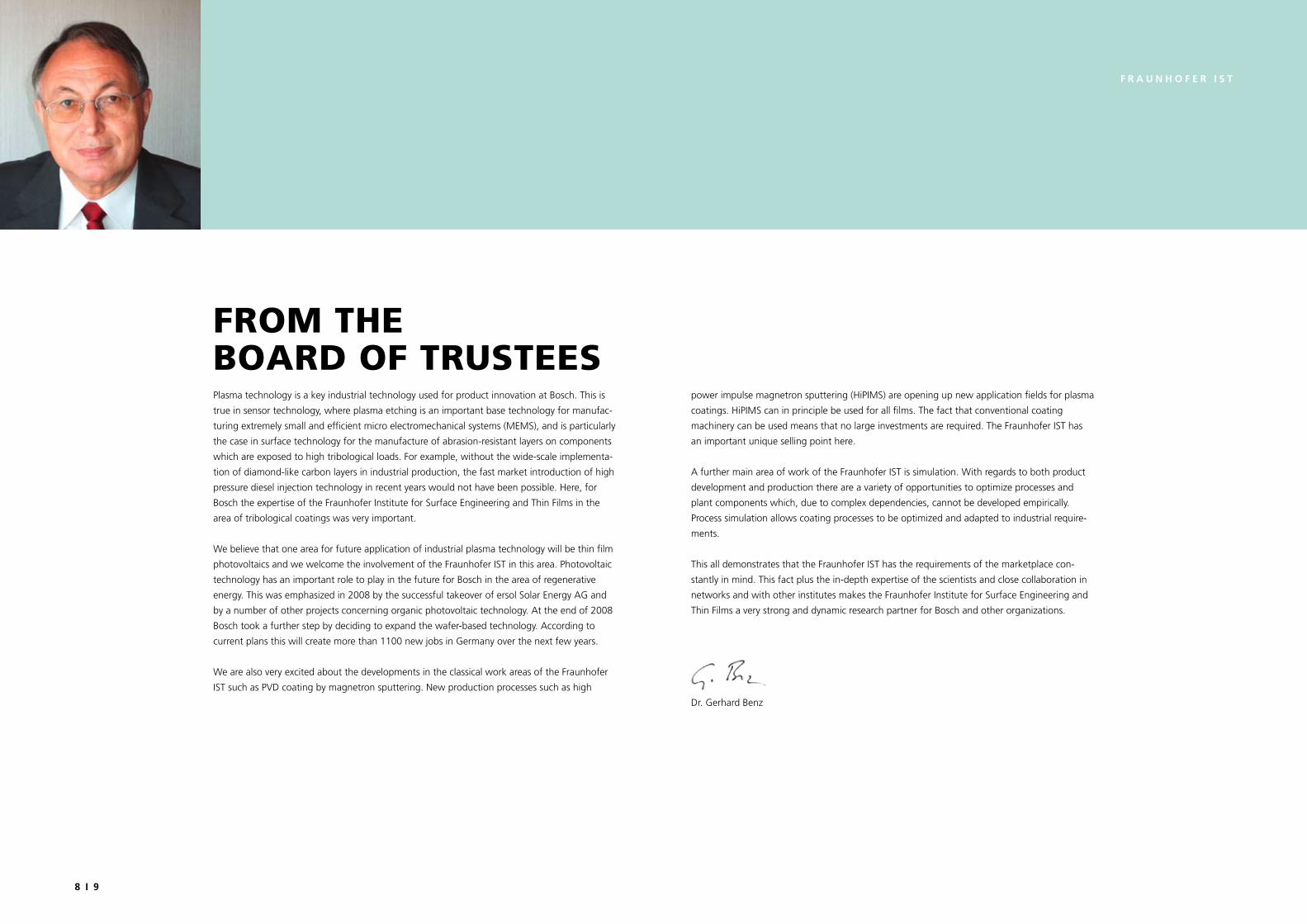
FoRewoRd1 Director Prof. Dr. Günter
Bräuer and deputy Dipl.-Ing.
Wolfgang Diehl with coated
glass panel.
1
Prof. Dr. Günter Bräuer Dipl.-Ing. Wolfgang Diehl

4 I 5
F r a u n h o F e r I S T
contentsForeword 3 Contents 4 Highlights 2008 6 Board of Trustees 8 Institute Profile 12 Budget of the Fraunhofer IST 14 Contact and Organizational Chart 17 The Scope of Research and Services 20
research news
Mechanical and Automotive Engineering 23 Characterization of carbon coatings in the ball-disk test by means of DOE methods 24
Carbon coatings in the rolling test: step by step to industrial applications 26
Force sensor systems with long-term stability by encapsulation of piezoresistive layers in the pressure diecasting process 28
Ionic liquids: electrodeposition differently for once 30 New materials for sputter strain gauges 32
Tools 35 Optimized control of deep-drawing processes via dies with integrated thin-film sensor 36
Influence of different plasma nitriding treatments on the wear behaviour of forging tools 38
Development of a duplex process consisting of plasma nitriding and DLC coating 40
Energy, Glass and Facade 43 Deposition of amorphous silicon films by gas flow sputtering 44
Development of a duplex process consisting of plasma nitriding and DLC coating 46
TCO high-performance thin films with HiPIMS 48
Optics, Information and Communication 51 Further development of HiPIMS technology for optical coatings 52
Sputter deposition of hot targets 54 In-situ measurement techniques for the optimization of dielectric filters 56
Piezoelectric coatings for microelectromechanical systems 58
Low-temperature bonding for silicon and glass 60
Wear-resistant electrically conductive coatings (M-A-X coatings) 62
Life Science and Ecology 65 Gas sensors based on titanium dioxide for detecting oxygen at low temperatures 66
Surface functionalization of threedimensional components by means of atmospheric-pressure plasma 68
Coating the inside of PCR tubes using atmospheric pressure plasma 70
Services and Competencies 73 Measuring the viscoelastic properties of SU8 polymer films during crosslinking 74
PACVD with microwave excitation 76 Calibration of a Seebeck measuring station 78 The next generation of sputtering? High power impulse magnetron sputtering (HiPIMS/HPPMS) 80
Simulation of gas flows and gas discharges with PICMC 82
Production technology for the generation of functional surfaces – status and perspectives 84
Fraunhofer IST sets up the first international patent database for plasma technology 86
Stepping into Mac Gyvers Shoes – The physics laboratory assistant training at Fraunhofer IST 88
Names, Dates, Events 2008 90 Exhibitions and Conferences 92 Workshops 94 Events and Prices 96 Scientific Publications 98
Networking of Fraunhofer IST 119 The Fraunhofer-Gesellschaft at a Glance 121 Fraunhofer Surface Technology and Photonics Alliance 122
INPLAS - Network of Competence Industrial Plasma Surface Technology 124
Memberships 126
List of Figures 127 Imprint 128
6 I 7
F r a u n h o F e r I S T
Blue-ray discs, terabyte hard drives, solar cells or flexible electronics – plasma technology as
an engine driving innovation is constantly coming up with new products. Plasma, whether in
vacuum or in atmosphere, will stay a key tool in the future as well when it is a matter of ex-
ploiting the physical properties of thin films to create innovations or even just to make surfaces
even more perfect.
Further development of core competences in the field of plasma-based coating processes was
one of the main emphases in work at the Fraunhofer IST in 2008 as well. With high-power
impulse magnetron sputtering it is possible to obtain plasmas with a high proportion of ionized
layer-forming atoms and thus coatings with completely new and improved properties. Our insti-
tute is implementing this technology in several departments and for different applications. Even
in the international arena we have thus already won an outstanding reputation for ourselves.
The situation is similar with gas-flow sputtering. In the meantime the corresponding coating
sources are also being used by different research partners in Europe and Japan and have dem-
onstrated their high potential for the production, for example, of photocatalytic (self-cleaning)
films as well as thermal insulation coatings on turbine blades.
So far the latest economic crisis has apparently not managed to impede the booming
photovoltaics industry in Germany. A market share of 30 % is forecast for thin-film cells by
the year 2020. The Fraunhofer IST is pursuing the goal of making itself into an internationally
recognized center of competence for thin-film photovoltaics. This is to involve close coordina-
tion and collaboration with renowned research partners in this field, such as the Fraunhofer ISE,
the Forschungszentrum Jülich and the HZB (Helmholtz Center for Materials and Energy - Berlin).
Thanks to the generous support of the executive board of the Fraunhofer Society it has already
been possible to make considerable investments and more are to follow in 2009. Shortly to
enter service is the multi-chamber continuous-type installation with hot-filament CVD processes
for the deposition of amorphous and microcrystalline silicon – very probably the first of its kind
in the world.
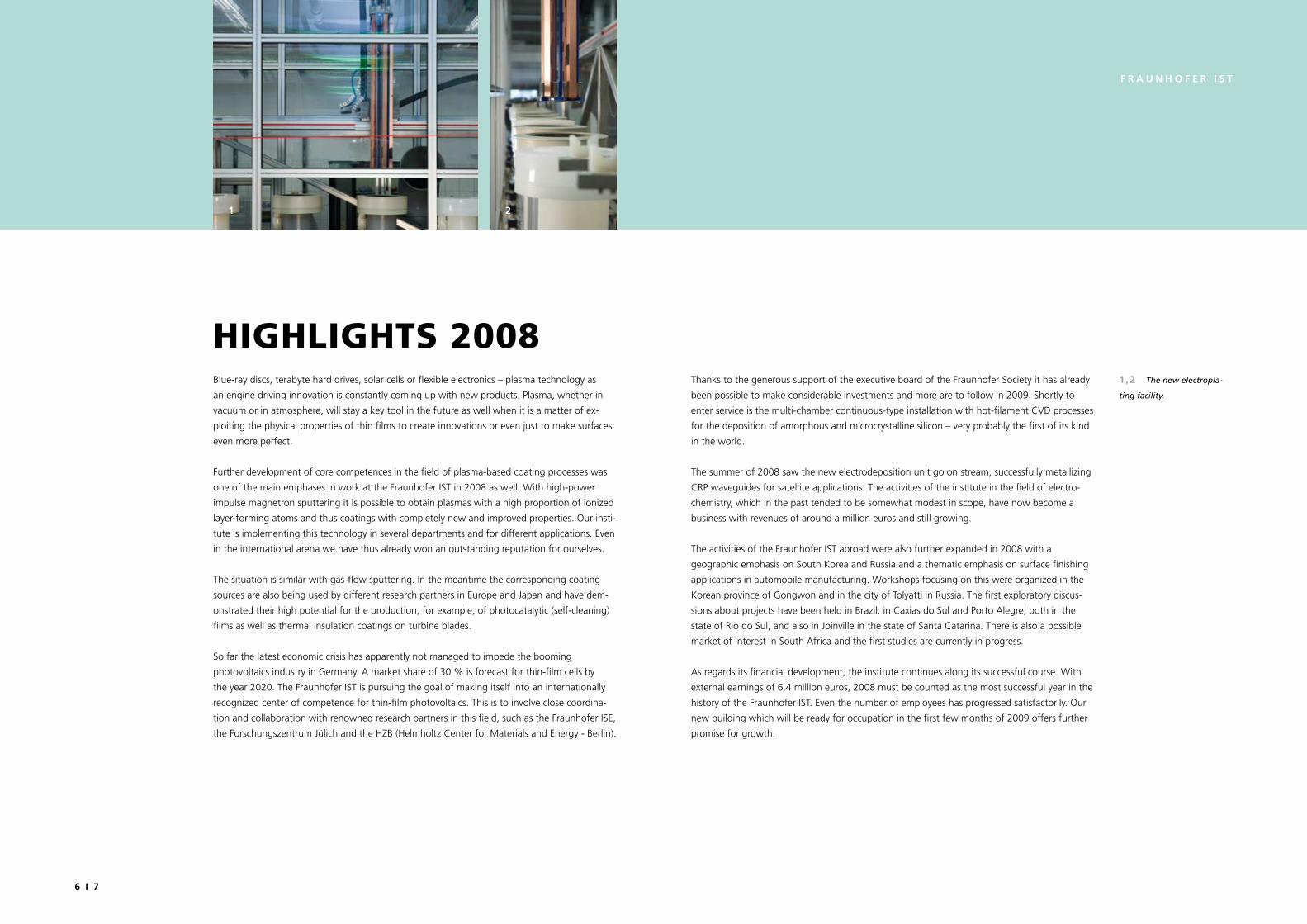
The summer of 2008 saw the new electrodeposition unit go on stream, successfully metallizing
CRP waveguides for satellite applications. The activities of the institute in the field of electro-
chemistry, which in the past tended to be somewhat modest in scope, have now become a
business with revenues of around a million euros and still growing.
The activities of the Fraunhofer IST abroad were also further expanded in 2008 with a
geographic emphasis on South Korea and Russia and a thematic emphasis on surface finishing
applications in automobile manufacturing. Workshops focusing on this were organized in the
Korean province of Gongwon and in the city of Tolyatti in Russia. The first exploratory discus-
sions about projects have been held in Brazil: in Caxias do Sul and Porto Alegre, both in the
state of Rio do Sul, and also in Joinville in the state of Santa Catarina. There is also a possible
market of interest in South Africa and the first studies are currently in progress.
As regards its financial development, the institute continues along its successful course. With
external earnings of 6.4 million euros, 2008 must be counted as the most successful year in the
history of the Fraunhofer IST. Even the number of employees has progressed satisfactorily. Our
new building which will be ready for occupation in the first few months of 2009 offers further
promise for growth.
HigHligHts 20081,2 The new electropla-
ting facility.
1 2
8 I 9
F r a u n h o F e r I S T
power impulse magnetron sputtering (HiPIMS) are opening up new application fields for plasma
coatings. HiPIMS can in principle be used for all films. The fact that conventional coating
machinery can be used means that no large investments are required. The Fraunhofer IST has
an important unique selling point here.
A further main area of work of the Fraunhofer IST is simulation. With regards to both product
development and production there are a variety of opportunities to optimize processes and
plant components which, due to complex dependencies, cannot be developed empirically.
Process simulation allows coating processes to be optimized and adapted to industrial require-
ments.
This all demonstrates that the Fraunhofer IST has the requirements of the marketplace con-
stantly in mind. This fact plus the in-depth expertise of the scientists and close collaboration in
networks and with other institutes makes the Fraunhofer Institute for Surface Engineering and
Thin Films a very strong and dynamic research partner for Bosch and other organizations.
Dr. Gerhard Benz
Plasma technology is a key industrial technology used for product innovation at Bosch. This is
true in sensor technology, where plasma etching is an important base technology for manufac-
turing extremely small and efficient micro electromechanical systems (MEMS), and is particularly
the case in surface technology for the manufacture of abrasion-resistant layers on components
which are exposed to high tribological loads. For example, without the wide-scale implementa-
tion of diamond-like carbon layers in industrial production, the fast market introduction of high
pressure diesel injection technology in recent years would not have been possible. Here, for
Bosch the expertise of the Fraunhofer Institute for Surface Engineering and Thin Films in the
area of tribological coatings was very important.
We believe that one area for future application of industrial plasma technology will be thin film
photovoltaics and we welcome the involvement of the Fraunhofer IST in this area. Photovoltaic
technology has an important role to play in the future for Bosch in the area of regenerative
energy. This was emphasized in 2008 by the successful takeover of ersol Solar Energy AG and
by a number of other projects concerning organic photovoltaic technology. At the end of 2008
Bosch took a further step by deciding to expand the wafer-based technology. According to
current plans this will create more than 1100 new jobs in Germany over the next few years.
We are also very excited about the developments in the classical work areas of the Fraunhofer
IST such as PVD coating by magnetron sputtering. New production processes such as high
FRom tHe BoARd oF tRustees
10 I 11
F r a u n h o F e r I S T
Chairman
Dipl.-Ing. R. LacherSingulus Technologies AG
Deputy
Prof. Dr. H. OechsnerIFOS - Institut für Oberflächen- und Schichtanalytik GmbH an der TU Kaiserslautern
Dr. G. BenzRobert Bosch GmbH
Prof. Dr. W. BlauEFDS Europäische Forschungs gesellschaft Dünne Schichten e. V.
Dipl.-Ing. E. DietrichFrankfurt
Dr. U. EngelMIBA AG
Dr. R. GrünPlaTeG GmbH
Prof. Dr.-Ing. Dr. h. c.
J. HesselbachPräsident der Technischen Universität Braunschweig
Dr. H. HilgersMainz
RD A. KletschkeBundesministerium für Bildung und Forschung
Dr. P. LichtenauerSoftal Electronic Erik Blumenfeld GmbH & Co. KG
Prof. Dr. A. MöbiusCookson Electronics Enthone GmbH
MinRat Dr. H. SchroederNiedersächsisches Ministerium für Wissenschaft und Kultur
Dr.-Ing. W. SteinbachBurgmann Industries GmbH & Co. KG
Dr.-Ing. M. SteinhorstDOC - Dortmunder OberflächenCentrum GmbH
Dr. G. J. van der KolkIonBond Netherlands BV
BoARd oF tRusteesDeath of Dr. Siegfried Döttinger, trustees board member
Employees at the Fraunhofer IST are mourning the death of Dr. Siegfried Döttinger, who passed
away in May 2008 after a protracted severe illness. Dr. Döttinger had been a member of our
board of trustees from 1998 until 2006 when he resigned from this honorary office for health
reasons.
The central task of his professional life had been to set up the surface technology department
at the Daimler Research and Technology Center in Ulm, Germany. Under his leadership a wide
range of competences were installed and interlinked, with the primary aim of creating and
making available the necessary foundations for the company and its products. Not only his
great scientific abilities but also his human qualities as regards leadership and employee training
as well as his knack at bringing together researchers from what were sometimes very different
corporate cultures, all made a decisive contribution to the success of his research department.
For almost ten years Dr. Döttinger accompanied the development of the Fraunhofer IST as a
trustee with an outstandingly high level of commitment. Here he was able to bring to bear his
extensive experience as a research manager for a major automobile group. His well-intentioned,
constructive criticism often helped us to find the right paths to take. Constantly he urged us to
tackle new directions in research and not to hesitate to drop the less attractive.
We have a great deal for which we must thank Dr. Döttinger and we will long cherish his
memory.
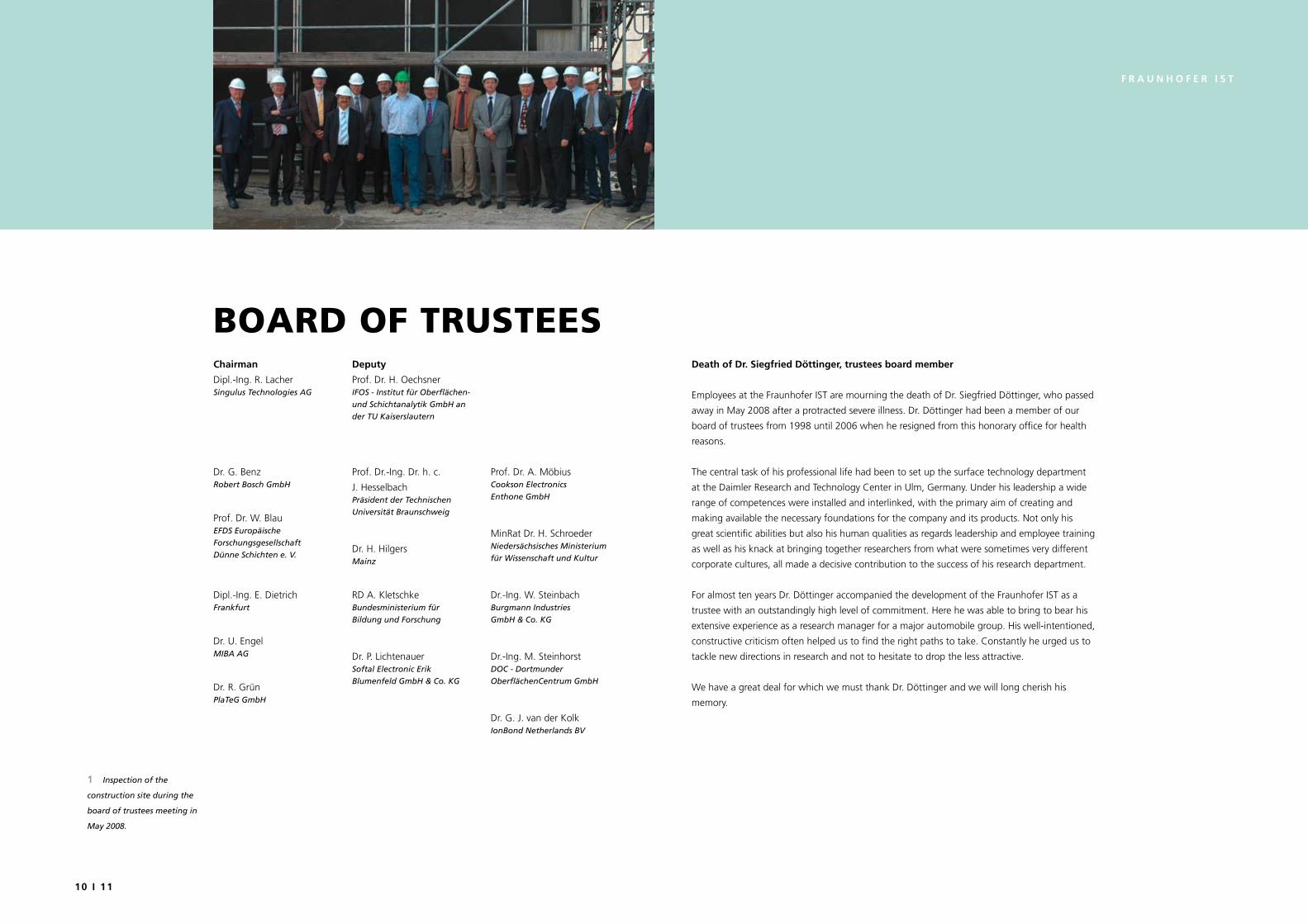
1 Inspection of the
construction site during the
board of trustees meeting in
May 2008.
12 I 13
F r a u n h o F e r I S T
As an industry oriented R&D service center, the Fraunhofer Institute for Surface Engineering
and Thin Films IST is pooling competencies in the areas film deposition, coating application, film
characterization, and surface analysis. A large number of scientists, engineers, and technicians
are busily working to provide various types of surfaces with new or improved func tions and,
as a result, help create inno vative marketable products. At pre sent, the institute’s business
seg ments are:
Mechanical and Automotive Engi neering Tools Energy, Glass and Facade Optics, Information and Com munications Life Science and Ecology
In pursuing these business segments the institute utilizes its competencies in
the following fields:
Low Pressure Processes Electrical and Optical Coa tings Super-hard Coatings Atmospheric Pressure Pro cesses Micro and Nano Technology Friction Reduction and Wear Protection Analysis and Testing
institute pRoFileIn line with the cross-sectional charac ter of coatings and surface technolo gies the institute
cooperates with a large number of coating service pro viders, equipment manufacturers, and
coating users from diverse in dus tries like machinery, transpor ta tion, pro duction technology,
electro nics, op tics, information technology, ener gy, medical devices, and biotech no lo gy to
name just the most im por tant ones.
On an office and laboratory area of more than 4000 square feet 85 tenu red employees are
addressing a variety of research projects. Its capa bilities are supplemented by the com petencies
of other institutes from the ”Fraunhofer Surface Techno lo gy and Photonics Alliance”. Many
projects are supported by funding through the state (Land) Nieder sachsen (Lower Sa xony), the
federal government, the Eu ropean Union, and other institutions.
Goals
Important goals of the Fraunhofer IST are
the rapid transfer of innovative solutions from application oriented research and develop- ment to the industrial praxis,
the establishment of new future oriented technologies in the market place and the transfer of these innovative technologies to small and medium sized companies.

14 I 15
F r a u n h o F e r I S T
Talent management
In the period under review the Fraunhofer IST employed 97
employees, more than half of whom are scientists or engi-
neers, plus nine doctoral students. In the laboratories, the
semi-technical facility, the workshops and offices our research
work is supported by technical and commercial staff as well as
by around 60 graduands and student assistants. In addition,
five young persons are undergoing training for their careers in
IT or as physics lab assistants.
Budget oF tHe FRAunHoFeR ist
operating budget
2008 saw an increase in the budget to 10.2 million euros
following the two previous years when the operating budget
remained unchanged at 9.5 million euros. In this growth,
payroll costs and material costs rose in the same proportion.
earnings structure
If the previous year had already seen a growth in revenues
from industry, there was a further increase in 2008 to 4.3
million euros. As regards public revenues, the result of the
previous year was barely maintained. Fortunately, revenues
from the European community have once again contributed to
creating a positive overall operational result for the institute.
Investments
In 2008 investments totaled 1.26 million euros, with project
investments making up only 11 % of this. 48 % of investment
spending was on ordinary investments and 41 % on strategic
investments.
Employees.
2001 02 03 04 05 06 07 08
100
80
60
40
20
0
10.000
8.000
6.000
4.000
2.000
02001 02 03 04 05 06 07 08
Personnel and material costs.
10.000
8.000
6.000
4.000
2.000
001 02 03 04 05 06 07 08
Revenue.
3.500
3.000
2.500
2.000
1.500
1.000
500
001 02 03 04 05 06 07 08
Capital expenditure.
Cost of materials Earnings realized in the industrial sector Project investment
Personnel costs Earnings realized in the public sector Normal and strategic investments
Internal programs Initial Equipment
Basic financing
16 I 17
F r a u n h o F e r I S T
Prof. Dr. Günter Bräuer Dipl.-Ing. Wolfgang Diehl Dr. Simone Kondruweit
Dr. Klaus Bewilogua Dr. Jochen Brand Prof. Dr. Claus-Peter Klages Dr. Lothar Schäfer
Dr. Ralf Bandorf
Dr. Michael ThomasDr. Andreas Pflug
Dr. Peter Willich
Dr. Thomas Jung
Dr. Michael Vergöhl
Dr. Andreas Dietz
Dr. Bernd Szyszka
Dipl.-Ing. Saskia Biehl
Dipl.-Kaufm. Michael Kaczmarek
YouR contAct peRsonThe Fraunhofer Institute for Surface Engineering and Thin Films (IST) was founded in 1990
and is your contact point for all matters concerning thin film technology. The Fraunhofer IST
comprises the management and marketing departments and seven technical departments:
Transfer Center Tribology New Tribological Coatings Diamond Technology Optical and Electrical Coatings
Optical Coatings Sensoric Functional Coatings Micro and Sensor Technologies
Large Area Coatings Magnetron Sputtering Hollow Cathode Processes Simulation
Atmospheric Pressure Processes Electroplating Atmospheric Pressure Plasma Processes
Characterization of Materials and Layers
18 I 19
DIreCTor TranSFer CenTer TrIboloGy Dr.-Ing. Jochen Brand Telephone +49 531 2155-600 | [email protected]
Prof. Dr. Günter BräuerTelephone +49 531 [email protected]
Prototypes and small volume production | Device conceptions | Plasma diffusion | Cleaning technology
DorTmunDer oberFläChenCenTerDr.-Ing. Jochen BrandTelephone +49 531 2155-600 | [email protected]
DepuTy new TrIboloGICal CoaTInGS Dr. Klaus Bewilogua Telephone +49 531 2155-642 | [email protected]
Dipl.-Ing. Wolfgang DiehlTelephone +49 531 [email protected]
DLC, cBN, CNx, hard coatings | Wetting behaviour | Forming tools | Dry lubricants | PVD and PACVD processes
DIamonD TeChnoloGy Dr. Lothar Schäfer Telephone +49 531 2155-520 | [email protected]
Tools and components | Diamond electrodes for electrochemical applica-tions | Hot-filament CVD processes | Large-area hot-filament CVD systems | Hot-filament CVD of Silicon-based coatings
aDmInISTraTIon opTICal anD eleCTrICal CoaTInGS Dr. Michael Vergöhl Telephone +49 531 2155-640 | [email protected]
Dipl.-Kaufmann Michael KaczmarekTelephone +49 531 2155-220 | [email protected]
opTICal CoaTInGSDr. Michael VergöhlTelephone +49 531 2155-640 | [email protected]
Optical and electrical coatings | PVD/CVD technologies | Materials engineering
SenSorIC FunCTIonal CoaTInGSDr. Ralf BandorfTelephone +49 531 2155-602 | [email protected]
Multifunctional coatings with sensors | High Power Impulse Magnetron Sputtering (HiPIMS) | Microtribology
mICro anD SenSor TeChnoloGIeSDipl.-Ing. Saskia BiehlTelephone +49 531 2155-604 | [email protected]
Thin film sensors | Microstructuring 2D und 3D | Adaptronic systems
markeTInG anD CommunICaTIonS larGe area CoaTInGS Dr. Bernd Szyszka Telephone +49 531 2155-641 | [email protected]
Dr. Simone KondruweitTelephone +49 531 2155-535 | [email protected]
maGneTron SpuTTerInG
Dr. Bernd SzyszkaTelephone +49 531 2155-641 | [email protected]
Large area electronics | Process technology | Transparent and conductive coatings | Process simulation
hollow CaThoDe proCeSSeSDr. Thomas JungTelephone +49 531 2155-616 | [email protected]
Plasma sources | High rate processes | Oxide and carbon films
SImulaTIonDr. Andreas PflugTelephone +49 531 2155-629 | [email protected]
Anlagen- und Prozessentwicklung | Simulation von Schichteigenschaften | Virtuelle Prozessanalyse
aTmoSpherIC preSSure proCeSS Prof. Dr. Claus-Peter Klages Telephone +49 531 2155-510 | [email protected]
aTmoSpherIC preSSure plaSma proCeSSeSDr. Michael ThomasTelephone +49 531 2155-525 | [email protected]
Adhesion promotion | Chemical surface functionalization | Plasma clean-ing | Micro plasmas
eleCTroplaTInGDr. Andreas DietzTelephone +49 531 2155-646 | [email protected]
Composites | Light metal coatings | Process development | Plating on plastics
CharaCTerIzaTIon oF maTerIalS Dr. Peter Willich Telephone +49 531 2155-570 | [email protected]
analySISDr. Peter WillichTelephone +49 531 2155-570 | [email protected]
Micro and surface analysis | Microscopy and structure analysis | Industrial services
QualITy ConTrolDr. Peter WillichTelephone +49 531 2155-570 | [email protected]
Testing of coatings and materials | Development of testing procedures | Industrial serviceso
Rg
An
izA
tio
nA
l c
HA
Rt

20 I 21
F r a u n h o F e r I S T
analysis and Quality Control
High resolution scanning electron microscope with energy dispersive x-ray analysis (EDX)
Electron Probe Microanalysis (EPMA) Secondary-ion mass spectrometer X-ray diffraction equipment for structural analysis and for reflectivity measurement
Scanning tunnel and atomic force microscope Micro indenter and nano indenter for hardness and young’s modulus determination of coatings
Profilometer Automated, non-destructive measurement of film thickness Confocal scanning laser microscope Testing equipment for friction, wear and coating adhesion IR and UV-VIS spectrometer UV-VIS-NIR spectroscopic ellipsometer Equipment for surface energy measurement Equipment for corrosion and climatic testing according DIN EN
Measurement equipment for electrical and magnetical coating properties
VSM measuring station for magnetic films Systems for testing of electro chemical wastewater treat- ment
Equipment and methods for the characterization of the photo catalytical activity
p r e T r e a T m e n T
we clean surfaces
Successful coating processes imply a proper surface pretreat-
ment. Therefore we offer:
Effective aqueous surface cleaning including drying Special glass cleaning Plasma pretreatment Plasma cleaning Plasma activation Plasma functionalisation Wet-chemical etching pretreatment Particle beam
C o a T I n G
we develop processes and coating systems
Thin films are the core business of the Fraunhofer IST. The
institute utilizes a wide range of coating technologies, ranging
from plasma assisted deposition in vacuum and at atmospheric
pressure over hot-filament CVD processes to electroplating.
Our services are:
Development of coatings Process technology, including process diagnostics, modeling and control
Simulation of layer systems and processes
T e S T I n G / C h a r a C T e r I z a T I o n
we ensure quality
A fast and reliable analysis and quality control is the prerequi-
site for a successful coating development. We
offer our customers:
Test methods and product specific quality control methods, e. g. wear measurement on arbitrary parts
Ply adhesion Mechanical, chemical, micro morphological, and structural characterization
Optical and electrical charac te riza tion Rapid and confidential failure analysis
a p p l I C aT I o n
we transfer research results to the production level
To guarantee an efficient technology transfer we offer:
Cost-of-ownership calculations, development of economical production scenarios
Prototype development, pilot production and sample coating procedures
Equipment concepts and integra tion into manufacturing lines
Consulting and training Research and development during production
Special equipment
a-C:H:Me, a-C:H, hard coating production plant (up to 3 m3 volume)
Coating facilities incorporating magnetron and RF diode sputtering
Coating systems for hollow cathode processes Plasma-activated CVD (PACVD) units Plants for plasma diffusion Hot-filament-CVD units for diamond coatings and silicon-based coatings (up to 50 × 100 cm2)
In-line coating facility for large-surface optical functional coatings (up to 60 × 100 cm2)
Equipment for electroplating processes Photolithographic equipment (40 m 2 clean room)
15-stage cleaning unit for surface cleaning on aqueous basis
Laser for 3D microstructuring Atmospheric pressure plasma systems for coating and functionalization from microstructures up to large areas (40 × 100 cm2)
Industrial scale HiPIMS technology Two clean rooms with six coating units
tHe scope oF ReseARcH And seRvices
22 I 23
m e C h a n I C a l a n D a u T o m o T I v e e n G I n e e r I n G
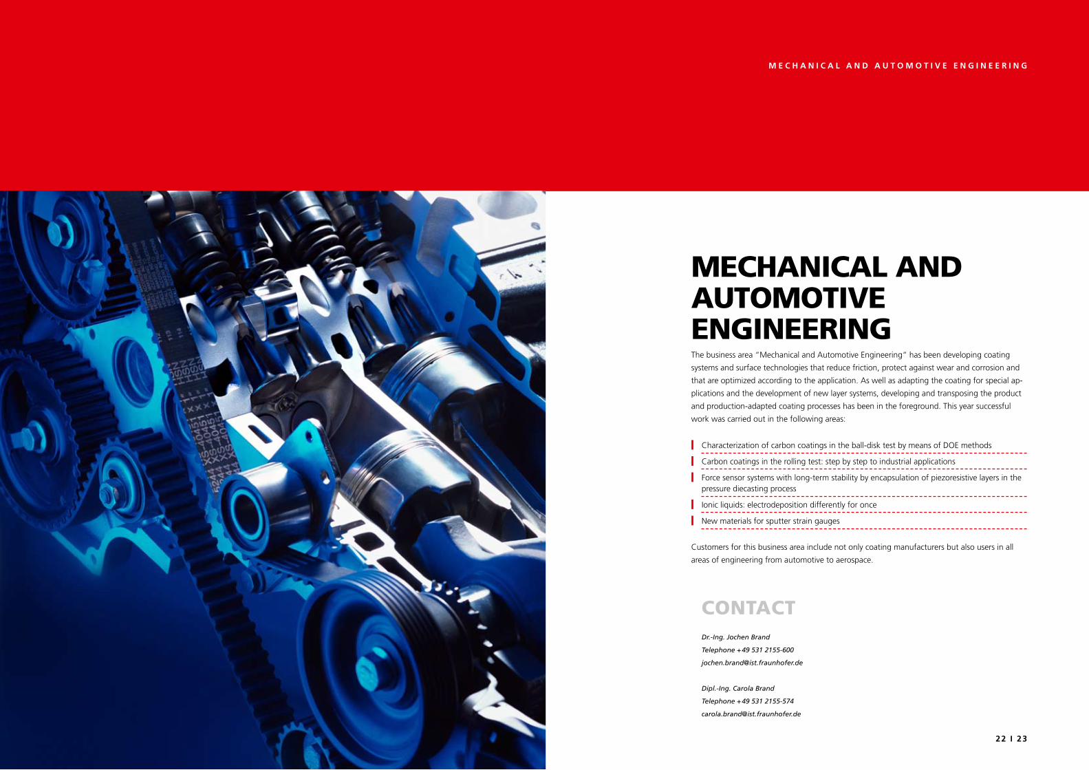
The business area “Mechanical and Automotive Engineering“ has been developing coating
systems and surface technologies that reduce friction, protect against wear and corrosion and
that are optimized according to the application. As well as adapting the coating for special ap-
plications and the development of new layer systems, developing and transposing the product
and production-adapted coating processes has been in the foreground. This year successful
work was carried out in the following areas:
Characterization of carbon coatings in the ball-disk test by means of DOE methods Carbon coatings in the rolling test: step by step to industrial applications Force sensor systems with long-term stability by encapsulation of piezoresistive layers in the pressure diecasting process
Ionic liquids: electrodeposition differently for once New materials for sputter strain gauges
Customers for this business area include not only coating manu facturers but also users in all
areas of engineering from automotive to aerospace.
8 I 9
mecHAnicAl And Automotive engineeRing
contActDr. -Ing. Jochen Brand
Telephone + 49 531 2155-600
Dipl. -Ing. Carola Brand
Telephone + 49 531 2155-574

24 I 25
m e C h a n I C a l a n D a u T o m o T I v e e n G I n e e r I n G
Speed of Master: UM
Speed of Slave: US
Force
Additional Heating
conducted at the Fraunhofer IST in order to characterize the
behavior of carbon coatings by means of DOE methods.
Test object and method
Within the context of the component design process the ques-
tion frequently arises as to which base material combined with
which coating system results in the best performance data.
In the investigations carried out at the IST, the family of DLC
coatings with three different substructures was characterized
in particular. In the first case the a-C:H overlay was attached
by means of titanium, in the second case by a gradient system
based on CrN, and in the third case also using titanium but
after a preceding plasma nitration of the corresponding base
material. The substrate materials selected were steels in com-
mon use, namely 100Cr6, 16MnCr5 and X155CrVMo12-1.
Tests aiming at obtaining a basic description were carried out
on a ball-disk test rig manufactured by the Wazau company.
Here in several tests the balls were sent skimming over a
flat substrate within a defined load and speed range. In this
way we determined, for example, the service life until layer
failure, the wear volume, the rate of wear and also friction
coefficients and friction loss. The test points within the
selected parameter window were defined as part of statistical
test planning in accordance with the DOE methods of ‘central
composite design’.
results
Statistical evaluation of the data meant that empirical models
could be created for every possible combination of layers
and materials in multidimensional regression analyses. These
models represent the corresponding behavior in the test in the
form of mathematical model equations as well as response
surfaces and Pareto analyses.
The results show tendencies in how the various coatings
behave on the three materials. It thus appears that with,
for example, the Ti+a-C:H coating on X155CrVMo21-1, the
increase in the sliding speed in the test has no significant influ-
ence on the service life. The CrN-supported C-DLC coating
here exhibits considerable dependencies – but still achieves a
service life one to twenty times longer and, due to its different
substructure, is on the whole much less sensitive to loading.
The findings obtained will in future simplify – by quantitative
and qualitative comparisons – the selection of suitable coating
systems and substrate materials for industrial applications.
Due to the constantly increasing demands made of steel
components in industrial applications the development and
special adaptation of new material concepts is becoming
more and more important. For tribological applications a
better knowledge of friction and wear characteristics is for this
reason urgently necessary. Basic investigations were therefore
cHARActeRizAtion oF cARBon coAtings in tHe BAll-disk test BY meAns oF doe metHods
1 Schematic of Ball-disk
contact during the test.
1
Response surface model of Ti + DLC coating on
X155CrVMo12-1.
contActDr.-Ing. Gerrit von Borries
Telephone +49 531 2155-662
26 I 27
m e C h a n I C a l a n D a u T o m o T I v e e n G I n e e r I n G
Speed of Master: UM
Speed of Slave: US
Force
Additional Heating
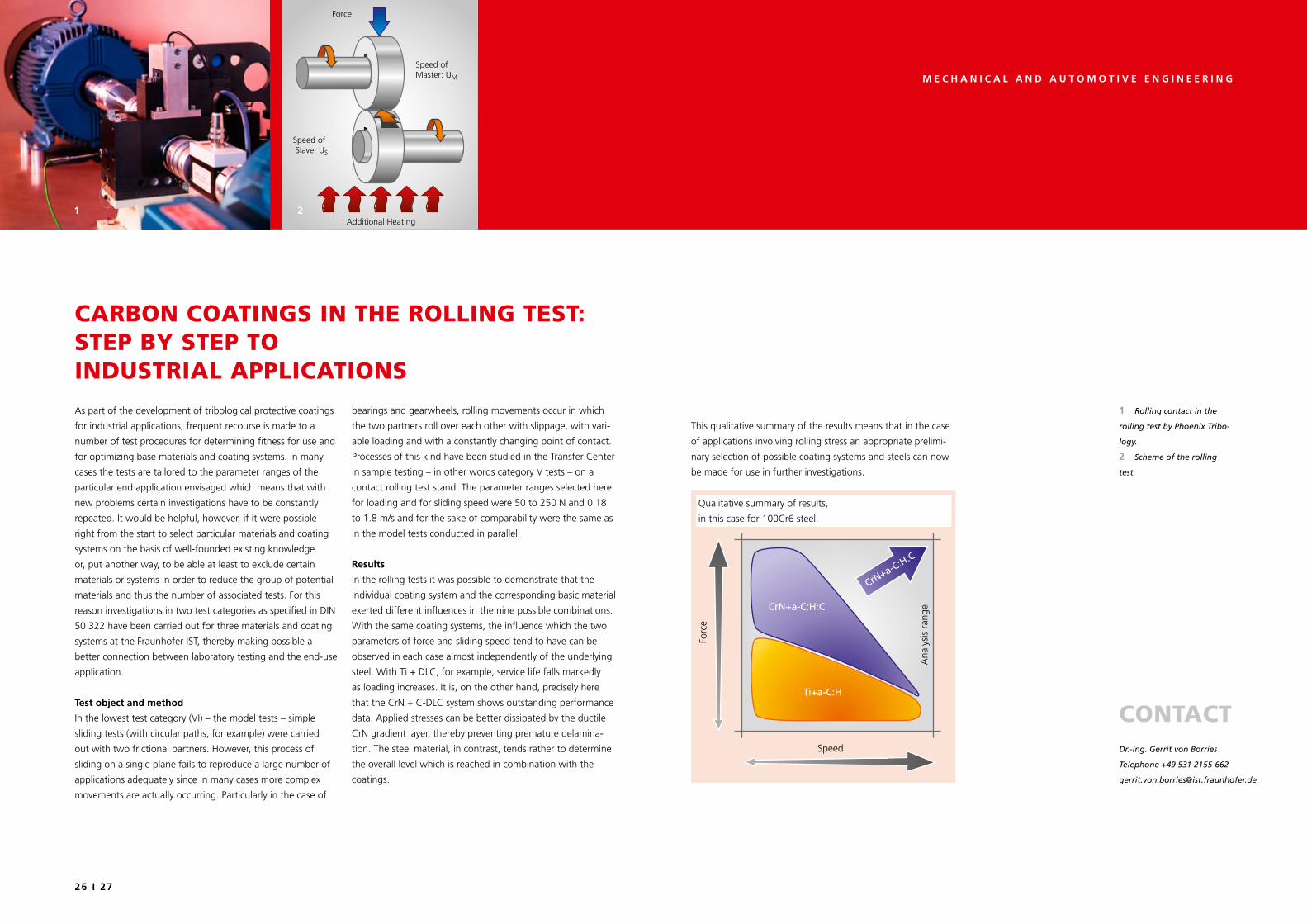
bearings and gearwheels, rolling movements occur in which
the two partners roll over each other with slippage, with vari-
able loading and with a constantly changing point of contact.
Processes of this kind have been studied in the Transfer Center
in sample testing – in other words category V tests – on a
contact rolling test stand. The parameter ranges selected here
for loading and for sliding speed were 50 to 250 N and 0.18
to 1.8 m/s and for the sake of comparability were the same as
in the model tests conducted in parallel.
results
In the rolling tests it was possible to demonstrate that the
individual coating system and the corresponding basic material
exerted different influences in the nine possible combinations.
With the same coating systems, the influence which the two
parameters of force and sliding speed tend to have can be
observed in each case almost independently of the underlying
steel. With Ti + DLC, for example, service life falls markedly
as loading increases. It is, on the other hand, precisely here
that the CrN + C-DLC system shows outstanding performance
data. Applied stresses can be better dissipated by the ductile
CrN gradient layer, thereby preventing premature delamina-
tion. The steel material, in contrast, tends rather to determine
the overall level which is reached in combination with the
coatings.
This qualitative summary of the results means that in the case
of applications involving rolling stress an appropriate prelimi-
nary selection of possible coating systems and steels can now
be made for use in further investigations.
As part of the development of tribological protective coatings
for industrial applications, frequent recourse is made to a
number of test procedures for determining fitness for use and
for optimizing base materials and coating systems. In many
cases the tests are tailored to the parameter ranges of the
particular end application envisaged which means that with
new problems certain investigations have to be constantly
repeated. It would be helpful, however, if it were possible
right from the start to select particular materials and coating
systems on the basis of well-founded existing knowledge
or, put another way, to be able at least to exclude certain
materials or systems in order to reduce the group of potential
materials and thus the number of associated tests. For this
reason investigations in two test categories as specified in DIN
50 322 have been carried out for three materials and coating
systems at the Fraunhofer IST, thereby making possible a
better connection between laboratory testing and the end-use
application.
Test object and method
In the lowest test category (VI) – the model tests – simple
sliding tests (with circular paths, for example) were carried
out with two frictional partners. However, this process of
sliding on a single plane fails to reproduce a large number of
applications adequately since in many cases more complex
movements are actually occurring. Particularly in the case of
cARBon coAtings in tHe Rolling test: step BY step to industRiAl ApplicAtions
1 Rolling contact in the
rolling test by Phoenix Tribo-
logy.
2 Scheme of the rolling
test.
1 2
Speed
Ana
lysi
s ra
nge
Ti+a-C:H
CrN+a-C:H:C
CrN+a-C:H:C
Forc
e
Qualitative summary of results,
in this case for 100Cr6 steel.
contActDr.-Ing. Gerrit von Borries
Telephone +49 531 2155-662

28 I 29
m e C h a n I C a l a n D a u T o m o T I v e e n G I n e e r I n G
sensors cannot be used with static measurements and do not
permit preloading settings. The force-sensor coating DiaForce®
which is based on a diamond-like hydrocarbon layer is able to
measure both static and dynamic forces. It is a tribologically
loadable coating (hardness: 20 GPa) which measures directly in
the main loading zones without elastic deformation. Coating
thickness is around 6 µm. Sensor systems of the washer type
are structured such that the coated surfaces are enclosed
by gluing from the outside. This encapsulation does not
have sufficient long-term stability and is poorly reproducible.
With the pressure diecasting and the chill casting processes
the Fraunhofer IFAM has succeeded in giving these thin-film
systems a stable sheathing (pictures 1 and 2). Here the direct
contact of the aluminum melt at a temperature of 700 °C with
the thin-film sensor, whose total thickness is 9 µm, has an
influence on the sensitivity of the sensor. The coating system
is shown in the left-hand figure. The sensor characteristics are
irreversibly changed by the casting process. This makes itself
noticeable in lower sensor resistances. The linear dependence
of the sensor resistance on load before encapsulation is shown
in the right-hand figure. The characteristic change in resistance
amounts to approximately 1 Ohm/N. After the casting process
this linear dependence shifts to considerably lower resistances
and the change in resistance is in the region of 0.06 Ohm/N.
outlook
Encapsulation of thin-film systems in casting processes is a
very promising possibility for inexpensively producing robust
sensor systems with long-term stability and on an industrial
scale. Further optimization steps are required here to obtain
the best possible piezoresistivity of the thin-film system.
Piezoresistive thin-film sensors are characterized by being able
to detect static and dynamic loads without elastic deforma-
tion. When used for industrial applications the corresponding
sensor systems must be protected against environmental
influences and mechanical damage. This is done by encapsula-
tion. Joining is carried out by gluing methods which do not
however offer long-term stability, have poor reproducibility
and cannot be readily automated. In collaboration with the
Fraunhofer Institute for Manufacturing Technology and
Applied Materials Research (IFAM), casting processes have
been developed which assure long-term stability in encapsu-
lated thin-film sensor systems.
State of the art and possible solutions
The use of force sensor modules based on strain gauges
or piezoelectric materials implies an additional mass and
elasticity, as well as high costs. Conventional piezoelectric
FoRce sensoR sYstems witH long-teRm stABilitY BY encApsulAtion oF piezoResistive lAYeRs in tHe pRessuRe diecAsting pRocess
1 2
1 Sensor system embedded
by the pressure casting pro-
cess at 700° C.
2 Cast-in washer sensor
system.Strain-dependent resistance characteristic curve
before and after casting process.
35,4
35,5
35,6
35,7
0 1 2 3 4 5
580
582
584
0 1 2 3 4 5
Force [kN]
Resi
stan
ce [k
Ohm
]
Force [kN]
Resi
stan
ce [k
Ohm
]
1. Strain
1. Release
2. Strain
2. Release
3. Strain
3. Release
contActDipl.-Ing. Saskia Biehl
Telephone +49 531 2155-604
Substrate
DiaForce® (d=6 µm) sensor coating
Electrode structures made of chromium (d=0.2 µm)
Insulating and wear protection layer (d= 3 µm)
Structure of a thin-film force sensor.
30 I 31
m e C h a n I C a l a n D a u T o m o T I v e e n G I n e e r I n G
State of the art and possible solutions
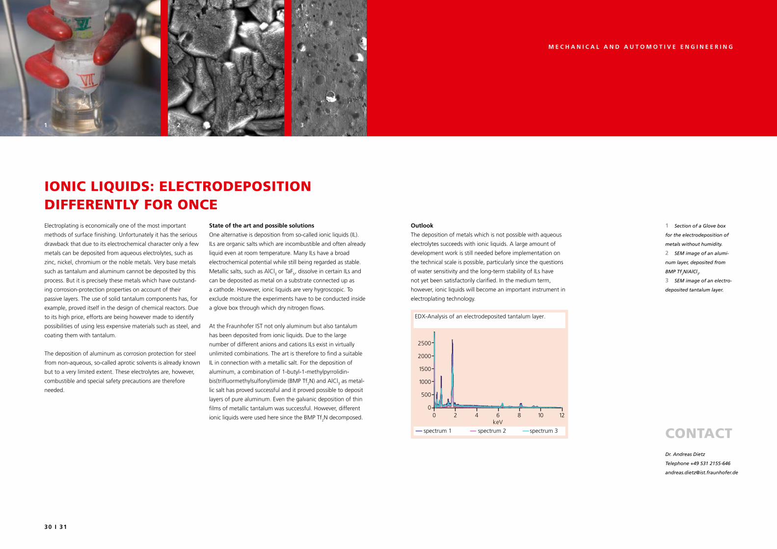
One alternative is deposition from so-called ionic liquids (IL).
ILs are organic salts which are incombustible and often already
liquid even at room temperature. Many ILs have a broad
electrochemical potential while still being regarded as stable.
Metallic salts, such as AlCl3 or TaF5, dissolve in certain ILs and
can be deposited as metal on a substrate connected up as
a cathode. However, ionic liquids are very hygroscopic. To
exclude moisture the experiments have to be conducted inside
a glove box through which dry nitrogen flows.
At the Fraunhofer IST not only aluminum but also tantalum
has been deposited from ionic liquids. Due to the large
number of different anions and cations ILs exist in virtually
unlimited combinations. The art is therefore to find a suitable
IL in connection with a metallic salt. For the deposition of
aluminum, a combination of 1-butyl-1-methylpyrrolidin-
bis(trifluormethylsulfonyl)imide (BMP Tf2N) and AlCl3 as metal-
lic salt has proved successful and it proved possible to deposit
layers of pure aluminum. Even the galvanic deposition of thin
films of metallic tantalum was successful. However, different
ionic liquids were used here since the BMP Tf2N decomposed.
outlook
The deposition of metals which is not possible with aqueous
electrolytes succeeds with ionic liquids. A large amount of
development work is still needed before implementation on
the technical scale is possible, particularly since the questions
of water sensitivity and the long-term stability of ILs have
not yet been satisfactorily clarified. In the medium term,
however, ionic liquids will become an important instrument in
electroplating technology.
Electroplating is economically one of the most important
methods of surface finishing. Unfortunately it has the serious
drawback that due to its electrochemical character only a few
metals can be deposited from aqueous electrolytes, such as
zinc, nickel, chromium or the noble metals. Very base metals
such as tantalum and aluminum cannot be deposited by this
process. But it is precisely these metals which have outstand-
ing corrosion-protection properties on account of their
passive layers. The use of solid tantalum components has, for
example, proved itself in the design of chemical reactors. Due
to its high price, efforts are being however made to identify
possibilities of using less expensive materials such as steel, and
coating them with tantalum.
The deposition of aluminum as corrosion protection for steel
from non-aqueous, so-called aprotic solvents is already known
but to a very limited extent. These electrolytes are, however,
combustible and special safety precautions are therefore
needed.
ionic liquids: electRodeposition diFFeRentlY FoR once
1 2 3
1 Section of a Glove box
for the electrodeposition of
metals without humidity.
2 SEM image of an alumi-
num layer, deposited from
BMP Tf2N/AlCl3.
3 SEM image of an electro-
deposited tantalum layer.
contActDr. Andreas Dietz
Telephone +49 531 2155-646
EDX-Analysis of an electrodeposited tantalum layer.
0
500
1000
1500
2000
2500
0 2 4 6 8 10 12keV
spectrum 1 spectrum 2 spectrum 3
32 I 33
m e C h a n I C a l a n D a u T o m o T I v e e n G I n e e r I n G
Current developments in sputtering technology, such as
HiPIMS (High Power Impulse Magnetron Sputtering), are being
used to influence specific aspects of coating properties. The
aim is, for example, to possibly dispense with an annealing
stage at > 200 °C to pre-age the material. This would mean
that inexpensive polymer substrates could be used.
me-DlC coatings as strain gauge material
For a number of years now DLC (Diamond-Like Carbon) has
been successfully used in pressure sensors. Metal clusters in
the DLC coating offer the possibility of strain measurement
mainly independent of the ambient temperature. The figure
on the left shows the sensitivity to strain (gauge factor) of
different Me-DLC coatings. Ni-DLC (a-C:H:Ni) deliver a consid-
erably higher strain sensitivity compared with the gauge factor
of ~2 typical of metals.
outlook
The literature mentions self-compensated ITO compounds
which are suitable for high-temperature applications up to
over 1000 °C. These are very promising properties which are
actually under investigation at the IST. In optimizing material
properties efforts are made to apply near-industrial fabrication
processes and test methods for the strain gauge materials.
Important objectives are in particular short process times and a
high degree of stability in sensoric properties.
Strain gauges are used in many different applications for mea-
suring forces, strain, moments or pressure. Classic foil strain
gauges are glued onto the component. In some products this
method is already being replaced by sputter strain gauges,
such as in pressure sensors or digital scales, for example. New
materials with innovative properties can contribute to further
spreading the use of sputter strain gauges.
advantages of sputter strain gauges
The tolerances of a component are mostly unaffected by the
coating in the case of the sputter strain gauge since it is only a
few microns thick. Because adhesive and polymer foil are not
used, the swelling and creep due to ambient temperatures or
humidity are avoided. The result is a greater precision in strain
measurement with sputter strain gauges than with standard
foil strain gauges.
objectives of material development
Of particular interest is a strain gauge material with a
higher gauge factor which permits further improvement of
measurement precision. In addition, a negligible temperature
dependence of strain measurement is aimed at, as also the
smallest possible drift in the measurement signal. Furthermore,
material combinations for high-temperature applications are
being investigated which would be suitable for operating
temperatures above 600 °C, such as applies to measurements
in the exhaust gas system or in aircraft turbines.
new mAteRiAls FoR sputteR stRAin gAuges
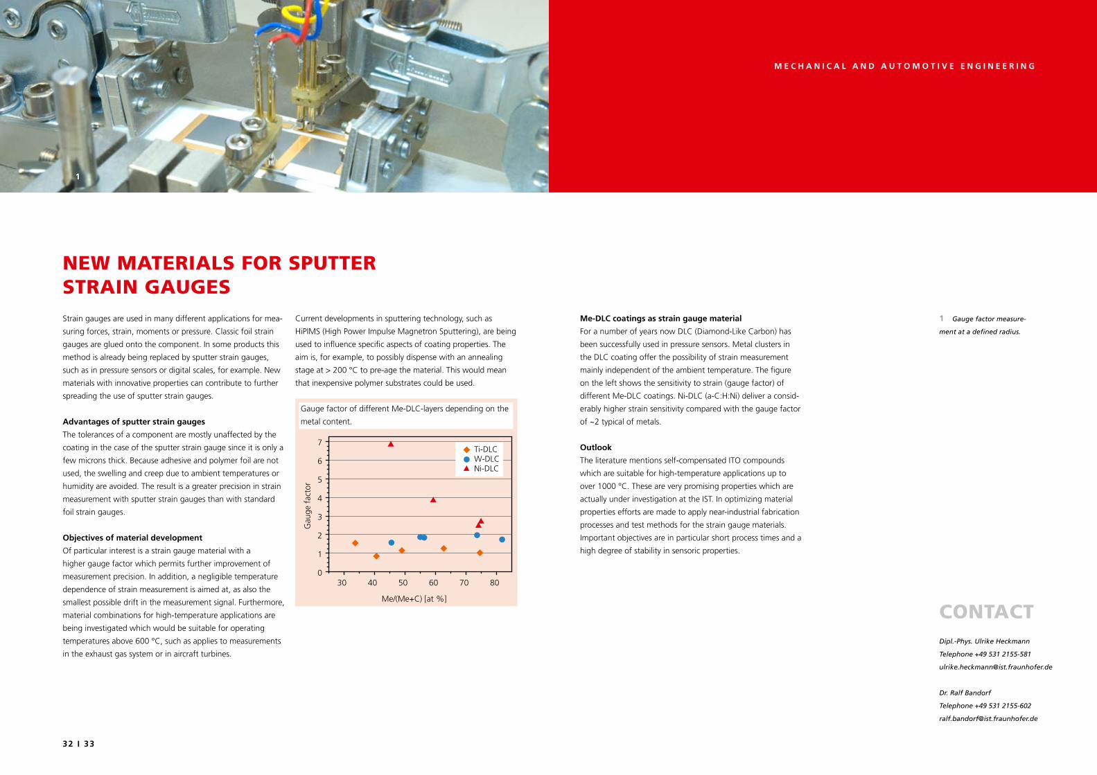
1 Gauge factor measure-
ment at a defined radius.
1
Ni-DLC
Me/(Me+C) [at %]
Gau
ge f
acto
r
W-DLCTi-DLC
30 40 50 60 70 800
1
2
3
4
5
6
7
Gauge factor of different Me-DLC-layers depending on the
metal content.
contActDipl.-Phys. Ulrike Heckmann
Telephone +49 531 2155-581
Dr. Ralf Bandorf
Telephone +49 531 2155-602
34 I 35
T o o l S
The IST is concentrating on the following topics within the business area ”Tools”:
Improving quality and per formance of forming and cutting processes using anti-adhesive coatings
Super hard coatings CompeDIA ® diamond grinding layers for precision grinding tools
Cubic boron nitride coatings for the machining of hardened steel Development of “smart tools” with integrated sensor functio nalities Development of nanostructured composite coatings
Important customers of this business area are not only job coating companies but also tool
manufacturers and tool end-users e. g. from the die and mould making and the automotive
industry.
8 I 9
tools
contActDr.-Ing. Jan Gäbler
Telephone +49 531 2155-625
Dr.-Ing. Martin Keunecke
Telephone +49 531 2155-652
36 I 37
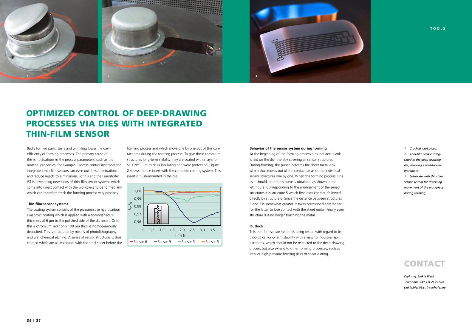
T o o l S
forming process and which move one by one out of this con-
tact area during the forming process. To give these chromium
structures long-term stability they are coated with a layer of
SiCON® 3 µm thick as insulating and wear protection. Figure
2 shows the die insert with the complete coating system. This
insert is flush-mounted in the die.
behavior of the sensor system during forming
At the beginning of the forming process a round steel blank
is laid on the die, thereby covering all sensor structures.
During forming, the punch deforms the sheet metal disk,
which thus moves out of the contact areas of the individual
sensor structures one by one. When the forming process runs
as it should, a uniform curve is obtained, as shown in the
left figure. Corresponding to the arrangement of the sensor
structures it is structure 5 which first loses contact, followed
directly by structure 6. Since the distance between structures
6 and 3 is somewhat greater, it takes correspondingly longer
for the latter to lose contact with the sheet metal. Finally even
structure 9 is no longer touching the metal.
outlook
This thin-film sensor system is being tested with regard to its
tribological long-term stability with a view to industrial ap-
plications, which should not be restricted to the deep-drawing
process but also extend to other forming processes, such as
interior high-pressure forming (IHP) or shear cutting.
Badly formed parts, tears and wrinkling lower the cost-
efficiency of forming processes. The primary cause of
this is fluctuations in the process parameters, such as the
material properties, for example. Process control incorporating
integrated thin-film sensors can even out these fluctuations
and reduce rejects to a minimum. To this end the Fraunhofer
IST is developing new kinds of thin-film sensor systems which
come into direct contact with the workpiece to be formed and
which can therefore track the forming process very precisely.
Thin-film sensor systems
The coating system consists of the piezoresistive hydrocarbon
DiaForce® coating which is applied with a homogeneous
thickness of 6 µm to the polished side of the die insert. Onto
this a chromium layer only 100 nm thick is homogeneously
deposited. This is structured by means of photolithography
and wet-chemical etching. A series of sensor structures is thus
created which are all in contact with the steel sheet before the
optimized contRol oF deep-dRAwing pRocesses viA dies witH integRAted tHin-Film sensoR
1 Cracked workpiece.
2 Thin-film sensor integ-
rated in the deep-drawing
die, showing a well-formed
workpiece.
3 Substrate with thin-film
sensor system for detecting
movement of the workpiece
during forming.
2 31
contActDipl.-Ing. Saskia Biehl
Telephone +49 531 2155-604
Time [s]
R x/R
0
Sensor 5Sensor 3Sensor 9Sensor 6
0 0,5 1,0 1,5 2,0 2,5 3,0 3,5
0,96
0,97
0,98
0,99
1,00
38 I 39
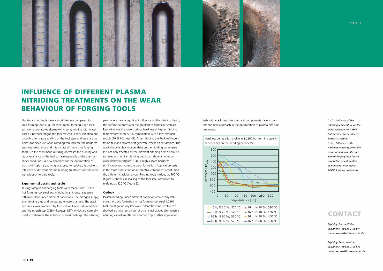
T o o l S
parameters have a significant influence on the nitriding depth,
the surface hardness and the gradient of hardness decrease.
Remarkable is the lower surface hardness at higher nitriding
temperatures (560 °C) in combination with a low nitrogen
supply (10 % N2, rest H2). After nitriding the Rockwell inden-
tation test and scratch test generate cracks on all samples. The
crack shape is clearly dependent on the nitriding parameters.
It is not only affected by the different nitriding depth because
samples with similar nitriding depth can show an unequal
crack behaviour (figure. 1-4). A high surface hardness
significantly promotes the crack formation. Application tests
in the mass production of automotive components confirmed
the different crack behaviour. Forging tools nitrided at 560 °C
(figure 6) show less spalling of the tool steel compared to
nitriding at 520 °C (figure 5).
outlook
Plasma nitriding under different conditions can clearly influ-
ence the crack formation in hot forming tool steel 1.2367.
First investigations by Rockwell indentation and scratch test
showed a similar behaviour of other steel grades after plasma
nitriding as well as after nitrocarburizing. Further application
tests with crack sensitive tools and components have to con-
firm the new approach in the optimization of plasma diffusion
treatments.
Usually forging tools have a short life-time compared to
cold forming tools e. g. for sheet metal forming. High local
surface temperatures alternately to spray cooling with water
based lubricants fatigue the tool material. Crack initiation and
growth often cause spalling of the tool steel and are starting
points for extensive wear. Nitriding can increase the hardness
and wear resistance and this is state of the art for forging
tools. On the other hand nitriding decreases the ductility and
crack resistance of the tool surface especially under thermal
shock conditions. A new approach for the optimization of
plasma diffusion treatments was used to reduce this problem.
Influence of different plasma nitriding treatments on the wear
behaviour of forging tools.
experimental details and results
Testing samples and forging tools were made from 1.2367
hot forming tool steel and nitrided in an industrial plasma
diffusion plant under different conditions. The nitrogen supply,
the nitriding time and temperature were changed. The crack
behaviour was examined by the Rockwell indentation method
and the scratch test (CSEM Revetest-RST), which are normally
used to determine the adhesion of hard coatings. The nitriding
inFluence oF diFFeRent plAsmA nitRiding tReAtments on tHe weAR BeHAviouR oF FoRging tools
1–4 Influence of the
nitriding temperature on the
crack behaviour of 1.2367
hot forming steel evaluated
by scratch testing.
5,6 Influence of the
nitriding temperature on the
crack formation on the sur-
face of forging tools for the
production of automotive
components after approx.
14.000 forming operations.
3 5 61 2 4
contActDipl.-Ing. Martin Weber
Telephone +49 531 2155-507
Dipl.-Ing. Peter Kaestner
Telephone +49 531 2155-573
6 h, N 20 %, 520 °C
2 h, N 20 %, 520 °C
16 h, N 20 %, 520 °C
16 h, N 80 %, 520 °C
16 h, N 10 %, 520 °C
16 h, N 10 %, 560 °C
16 h, N 10 %, 460 °C
16 h, N 80 %, 560 °C
Edge distance [µm]
Har
dnes
s [H
V0,
05]
0 50 100 150 200 250 300400
600
800
1000
1200
1400
1600
1800
Hardness penetration profile in 1.2367 hot forming steel in
dependency on the nitriding parameters.
40 I 41
T o o l S
same installation. The nitriding time, nitriding temperature,
plasma power, temperature control during heating and nitrid-
ing were varied, as too process control at the transition from
nitriding to coating (single-stage, two-stage with interruption).
Coating with a-C:H was carried out by a standardized process
under constant conditions. Different test geometries were
used (flat substrates, cutters, massive geometries) in order
to be able to cover a wide range of components later on.
Coatings produced by the duplex process were investigated
with regard to adhesive strength and the failure mechanisms
in the case of overloading. Here the Rockwell test (Figure
1-3) and scratch testing were used. At the end of process
development it was possible to produce DLC coatings with
outstanding adhesive strength and loadability on different
test substrates. It is worth noting that the first cracks in the
scratch test (Lc1), which indicate overloading, did not occur
until the load was about twice as high as with all previously
tested a-C:H coatings with a metallic adhesion layer. For many
applications a drawback is the slight roughening of the surface
due to plasma nitriding. To counteract this, the coating can be
polished after nitriding without impairing coating adhesion.
Likewise process control can be interrupted after nitriding
and then restarted at a later time in the same or in a different
installation. This permits a wide range of process control
variants.
outlook
With the duplex process which has been developed a-C:H
coatings and their modifications (a-C:H:Si, a-C:H:Si:O) can
be deposited on 1.3343 (HSS) and 1.2379 steels with an
adhesive strength previously unattained. Further work will look
to investigating the application limits of the process in drilled
holes and grooves as well as adapting it to other steels. The
focus here is on applications for forming tools and cutters and
also gear wheels.
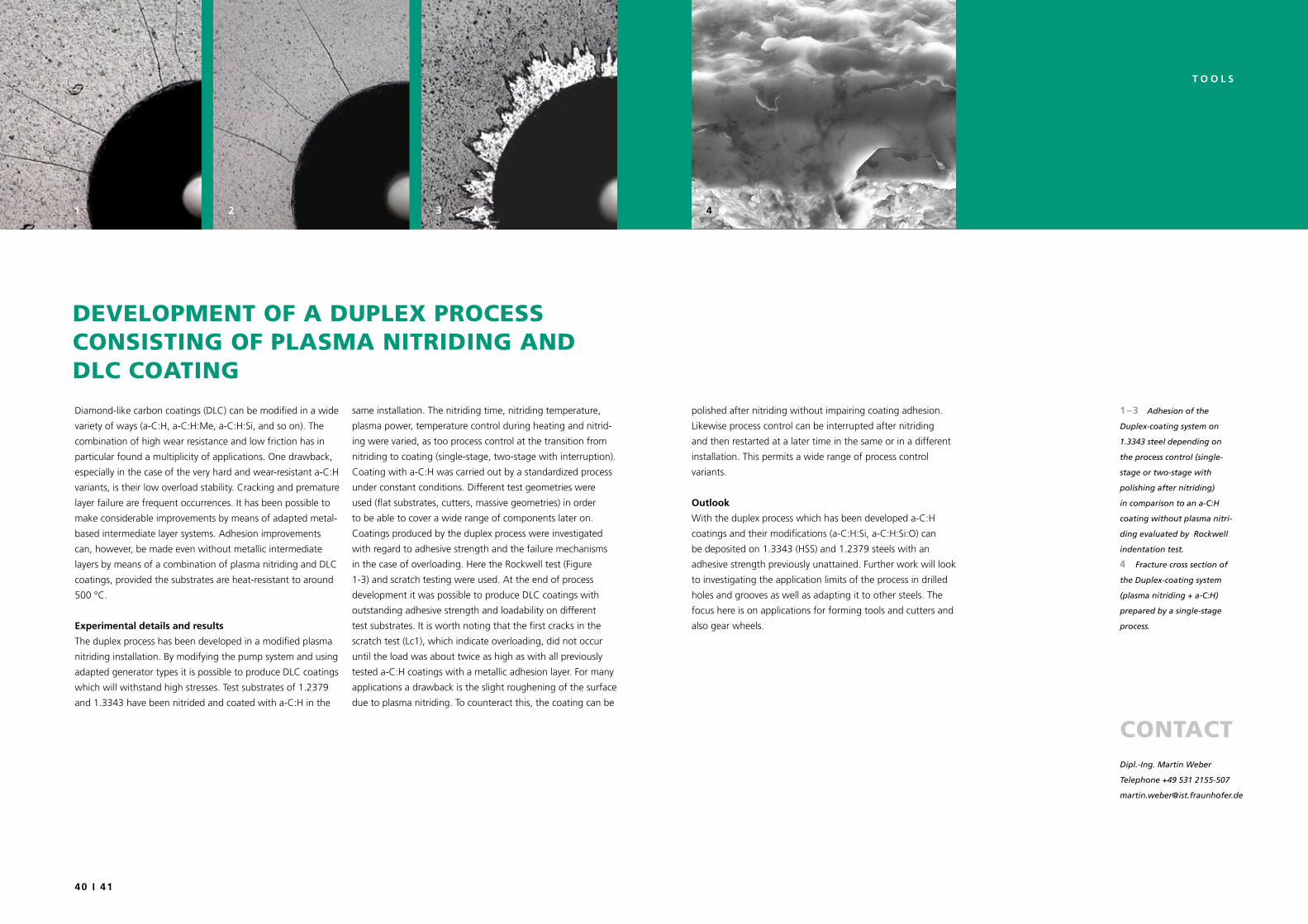
Diamond-like carbon coatings (DLC) can be modified in a wide
variety of ways (a-C:H, a-C:H:Me, a-C:H:Si, and so on). The
combination of high wear resistance and low friction has in
particular found a multiplicity of applications. One drawback,
especially in the case of the very hard and wear-resistant a-C:H
variants, is their low overload stability. Cracking and premature
layer failure are frequent occurrences. It has been possible to
make considerable improvements by means of adapted metal-
based intermediate layer systems. Adhesion improvements
can, however, be made even without metallic intermediate
layers by means of a combination of plasma nitriding and DLC
coatings, provided the substrates are heat-resistant to around
500 °C.
experimental details and results
The duplex process has been developed in a modified plasma
nitriding installation. By modifying the pump system and using
adapted generator types it is possible to produce DLC coatings
which will withstand high stresses. Test substrates of 1.2379
and 1.3343 have been nitrided and coated with a-C:H in the
development oF A duplex pRocess consisting oF plAsmA nitRiding And dlc coAting
1–3 Adhesion of the
Duplex-coating system on
1.3343 steel depending on
the process control (single-
stage or two-stage with
polishing after nitriding)
in comparison to an a-C:H
coating without plasma nitri-
ding evaluated by Rockwell
indentation test.
4 Fracture cross section of
the Duplex-coating system
(plasma nitriding + a-C:H)
prepared by a single-stage
process.
41 2 3
contActDipl.-Ing. Martin Weber
Telephone +49 531 2155-507
42 I 43
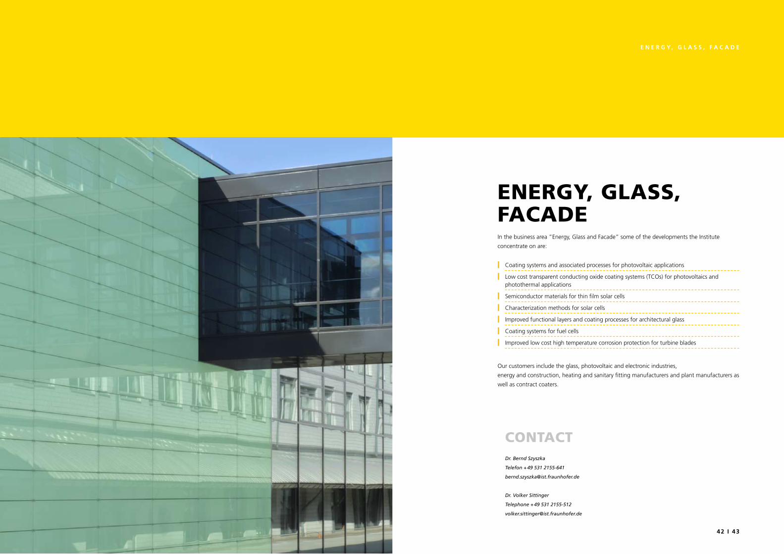
e n e r G y, G l a S S , F a C a D e
In the business area ”Energy, Glass and Facade” some of the developments the Institute
concentrate on are:
Coating systems and associated processes for photovoltaic applications Low cost transparent conducting oxide coating systems (TCOs) for photovoltaics and photothermal applications
Semiconductor materials for thin film solar cells Characterization methods for solar cells Improved functional layers and coating processes for architectural glass Coating systems for fuel cells Improved low cost high temperature corrosion protection for turbine blades
Our customers include the glass, pho to voltaic and electronic industries,
energy and construction, heating and sanitary fitting manufacturers and plant manufacturers as
well as contract coaters.
8 I 9
eneRgY, glAss, FAcAde
contActDr. Bernd Szyszka
Telefon + 49 531 2155-641
Dr. Volker Sittinger
Telephone + 49 531 2155-512
44 I 45
e n e r G y, G l a S S , F a C a D e
results
The silicon films were deposited in a coating plant with a
capacity of around 300 liters, equiped with a 250 mm GFS
linear source. To prevent ion damage in the coating system,
bombardment with argon ions was repelled by magnetic field
shielding. The substrates were AF45 glass and CZ-Si wafers
polished on both sides. It was possible to reduce the propor-
tion of foreign atoms in the a-Si:H layers by improving the
basic pressure (5x10⁻⁴ mbar) and leakage rate
(5x10⁻⁵ mbar l/s). A very complex parameter field was
investigated, with variations in pressure, gas composition
(Ar, H2), GFS performance, substrate temperature, bias and
frequencies. From the analytic point of view, FTIR, EPMA,
SIMS, XRD, SEM and conductivity measurements were applied.
The process was examined more precisely by means of
oscilloscopy and mass spectrometry.
Due to the low suction rate (250 m3/h) of the pumping system
the static deposition rate did not exceed more than 0.15 nm/s.
First results from the A700V in-line system (7000 m3/h) do,
however, indicate a rate of 5 nm/s. The H content in the films
can be set within a wide range (10-30 atom %) whereby the
proportion of foreign atoms is at minimum 3.3 atom %
(C: 0.8 / O: 1.5 / Ar: 1.0). The films typically exhibit very
smooth surfaces and are structureless in their morphology.
They consist of nanocrystals (approximately 1-2 nm) embed-
ded in an amorphous matrix. Investigations concerning the
light-to-dark conductivity revealed a marked improvement
in the 103 range due to magnetic field shielding – however,
good a-Si:H falls within the 105 range.
We were able to identify the reasons in the still excessively
high proportion of foreign atoms in the coatings and in
the coating plant respectively (due, in particular, to residual
moisture and volatile organic compounds from plastics).
outlook
On the basis of the results secured to date, gas flow sputtering
may be regarded as very promising for the field of thin-film
photovoltaics. In order to obtain further improvements in
deposition rates and semiconducting properties it is planned
to transfer the GFS linear source to the A700V large-area
coating plant.
1 R.J. Soukup et al., Solar Energy Materials & Solar Cells 91 (2007) 1383–1387
For almost 20 years the Fraunhofer IST has been working very
successful in the field of gas-flow-sputtering. The hollow-
cathode gas-flow-sputtering process allows soft deposition
conditions similar to those known from the chemical vapor de-
position process and is thus suitable for producing sputtered,
semiconducting a-Si:H and µc-Si:H films such as used in, for
example, the field of thin-film photovoltaics. In contrast to the
coating process otherwise used, the GSF method has no need
of toxic precursors. The high deposition rate, the simpleness of
upscaling, and integration into industrial in-line concepts are
further advantages.
For GFS tubular sources with magnetic field shielding it has
been already demonstrated to achieve light-to-dark conduc-
tivities of 106 in the batch process 1. As part of the research
described here the concept of magnetic field shielding has
been up-scaled to linear sources.
deposition oF AmoRpHous silicon Films BY gAs Flow sputteRing
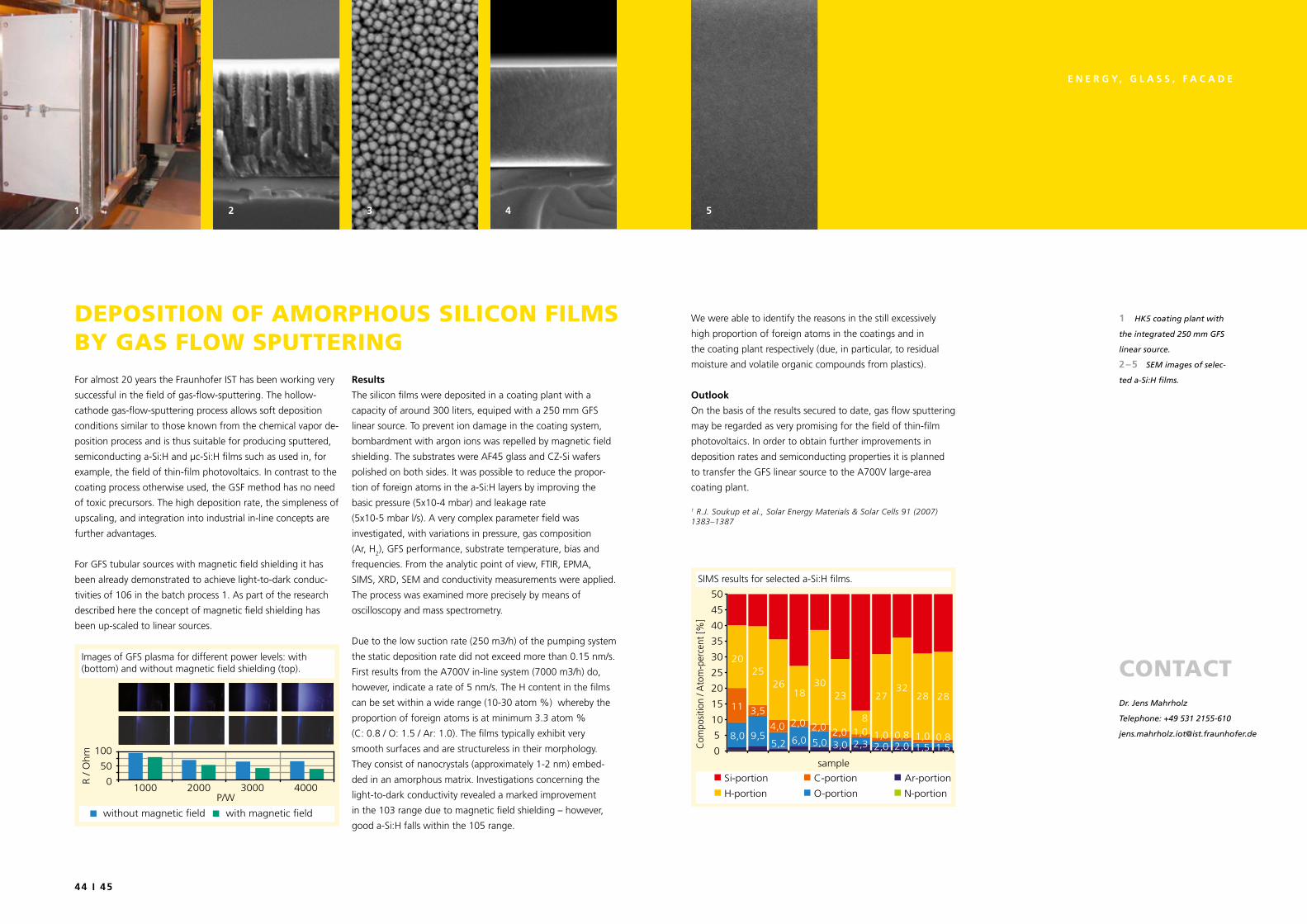
1 HK5 coating plant with
the integrated 250 mm GFS
linear source.
2–5 SEM images of selec-
ted a-Si:H films.
1 2 43 5
contActDr. Jens Mahrholz
Telephone: +49 531 2155-610
SIMS results for selected a-Si:H films.
8,0 9,55,2 6,0 5,0 3,0 2,3 2,0 2,0 1,5 1,5
11 3,5
4,0 2,0 2,0 2,0 1,0 0,8 1,0 0,81,0
2025
2618
3023
8
2732
28 28
0
5
10
15
20
25
30
35
40
45
50
sample
Com
posit
ion
/ Ato
m-p
erce
nt [%
]
Si-portion
H-portion
C-portion
O-portion
Ar-portion
N-portion0
50
100
3000 400020001000
without magnetic field
P/W
R /
Oh
m
with magnetic field
Images of GFS plasma for different power levels: with (bottom) and without magnetic field shielding (top).
46 I 47
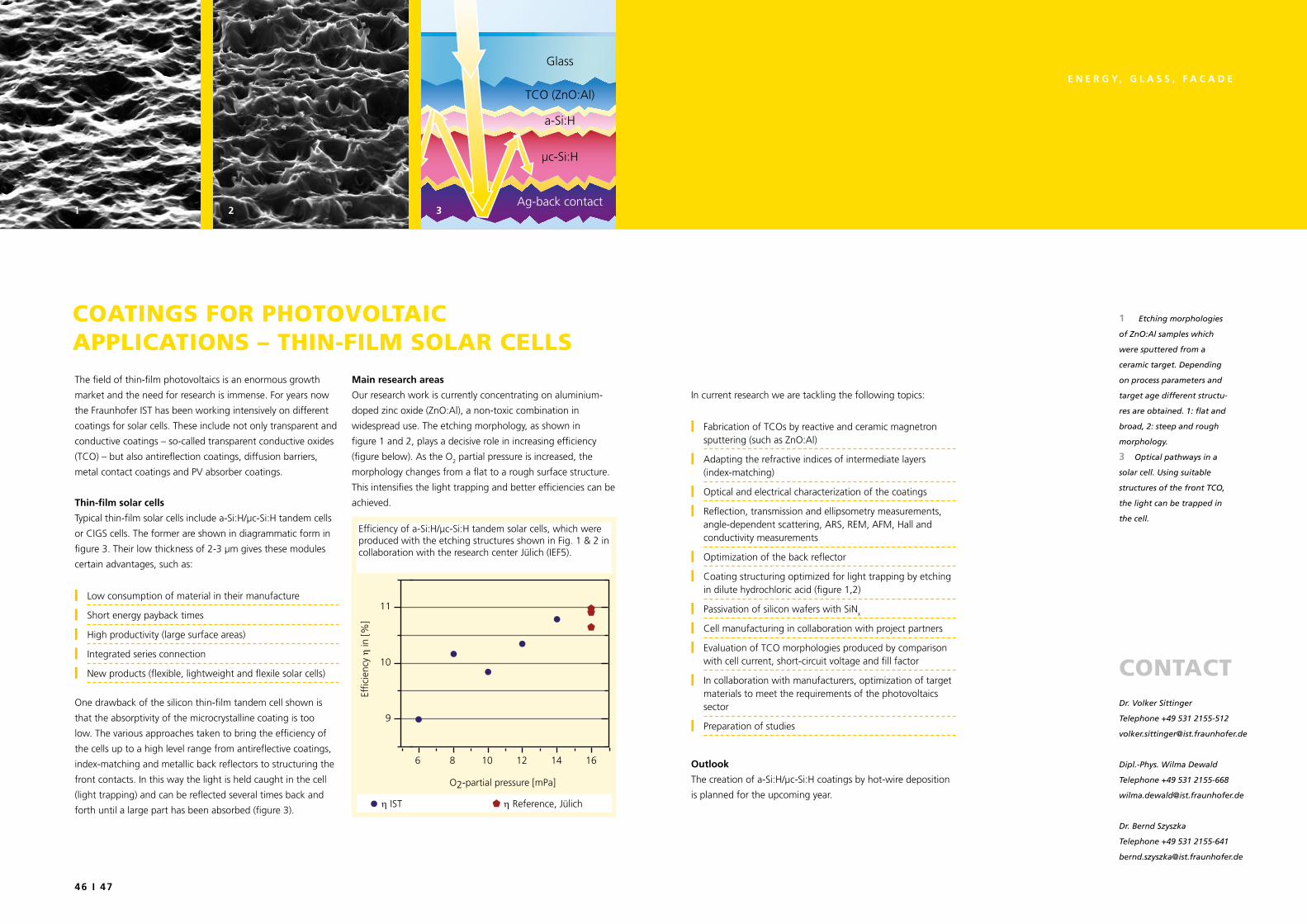
e n e r G y, G l a S S , F a C a D e
µc-Si:H
a-Si:H
TCO (ZnO:Al)
Glass
Ag-back contact
main research areas
Our research work is currently concentrating on aluminium-
doped zinc oxide (ZnO:Al), a non-toxic combination in
widespread use. The etching morphology, as shown in
figure 1 and 2, plays a decisive role in increasing efficiency
(figure below). As the O2 partial pressure is increased, the
morphology changes from a flat to a rough surface structure.
This intensifies the light trapping and better efficiencies can be
achieved.
In current research we are tackling the following topics:
Fabrication of TCOs by reactive and ceramic magnetron sputtering (such as ZnO:Al)
Adapting the refractive indices of intermediate layers (index-matching)
Optical and electrical characterization of the coatings Reflection, transmission and ellipsometry measurements, angle-dependent scattering, ARS, REM, AFM, Hall and conductivity measurements
Optimization of the back reflector Coating structuring optimized for light trapping by etching in dilute hydrochloric acid (figure 1,2)
Passivation of silicon wafers with SiN x
Cell manufacturing in collaboration with project partners Evaluation of TCO morphologies produced by comparison with cell current, short-circuit voltage and fill factor
In collaboration with manufacturers, optimization of target materials to meet the requirements of the photovoltaics sector
Preparation of studies
outlook
The creation of a-Si:H/µc-Si:H coatings by hot-wire deposition
is planned for the upcoming year.
The field of thin-film photovoltaics is an enormous growth
market and the need for research is immense. For years now
the Fraunhofer IST has been working intensively on different
coatings for solar cells. These include not only transparent and
conductive coatings – so-called transparent conductive oxides
(TCO) – but also antireflection coatings, diffusion barriers,
metal contact coatings and PV absorber coatings.
Thin-film solar cells
Typical thin-film solar cells include a-Si:H/µc-Si:H tandem cells
or CIGS cells. The former are shown in diagrammatic form in
figure 3. Their low thickness of 2-3 µm gives these modules
certain advantages, such as:
Low consumption of material in their manufacture Short energy payback times High productivity (large surface areas) Integrated series connection New products (flexible, lightweight and flexile solar cells)
One drawback of the silicon thin-film tandem cell shown is
that the absorptivity of the microcrystalline coating is too
low. The various approaches taken to bring the efficiency of
the cells up to a high level range from antireflective coatings,
index-matching and metallic back reflectors to structuring the
front contacts. In this way the light is held caught in the cell
(light trapping) and can be reflected several times back and
forth until a large part has been absorbed (figure 3).
coAtings FoR pHotovoltAic ApplicAtions – tHin-Film solAR cells
2 31
contActDr. Volker Sittinger
Telephone +49 531 2155-512
Dipl.-Phys. Wilma Dewald
Telephone +49 531 2155-668
Dr. Bernd Szyszka
Telephone +49 531 2155-641
Efficiency of a-Si:H/µc-Si:H tandem solar cells, which were produced with the etching structures shown in Fig. 1 & 2 in collaboration with the research center Jülich (IEF5).
Effic
ienc
y η
in [%
]
O2-partial pressure [mPa]
η IST η Reference, Jülich
11
10
9
6 8 10 12 14 16
1 Etching morphologies
of ZnO:Al samples which
were sputtered from a
ceramic target. Depending
on process parameters and
target age different structu-
res are obtained. 1: flat and
broad, 2: steep and rough
morphology.
3 Optical pathways in a
solar cell. Using suitable
structures of the front TCO,
the light can be trapped in
the cell.
48 I 49
e n e r G y, G l a S S , F a C a D e
applications
In addition, TCOs have spectrally selective optical properties.
Electrical conductivity is accompanied by high reflectivity in the
infrared spectral region (IR). This means that TCO films offer
low emissivity, such as is required, for example, to structure
non-fogging glazing elements. The problem of the inadequate
stability of a low-emitting coating system in Position 1 (exterior
coating) is solved by using the HiPIMS process. Under certain
impulse and power level conditions of film deposition at room
temperature, the texture and morphology of the coating can
be set such that it takes on the above-mentioned properties
during a subsequent annealing process (10 min at 650 °C). At
thicknesses of 140 nm the coatings reach a specific resistance
of 300 μΩcm with an optical transmission of 80 % on
2 mm float glass. Mechanical stability was verified by means
of abrasion testing. The measured variable for the amount of
specimen wear is the haze value in the transmitted light which
is due to surface changes and which results in the specimens
becoming hazy. Measurements which were carried out to
compare the different materials show that the ITO made by
HiPIMS exhibits the lowest proportion of scattered light and
thus the least wear. The SnO:F sample, on the other hand, has
detached completely from the substrate.
outlook
TCOs optimized with the help of the HiPIMS process are find-
ing future applications in displays, touchscreens, solar cells,
heating coatings and more.
Transparent conductive oxide contacts (TCOs) are a key
technology for the display and thin-film photovoltaics industry.
Tin-doped indium oxide (ITO) is used in the display industry as
a front contact on account of its very high optical transmission
capabilities and excellent electrical conductivity. The HiPIMS
technique can deliver very dense plasmas with a very high
degree of target material ionization.
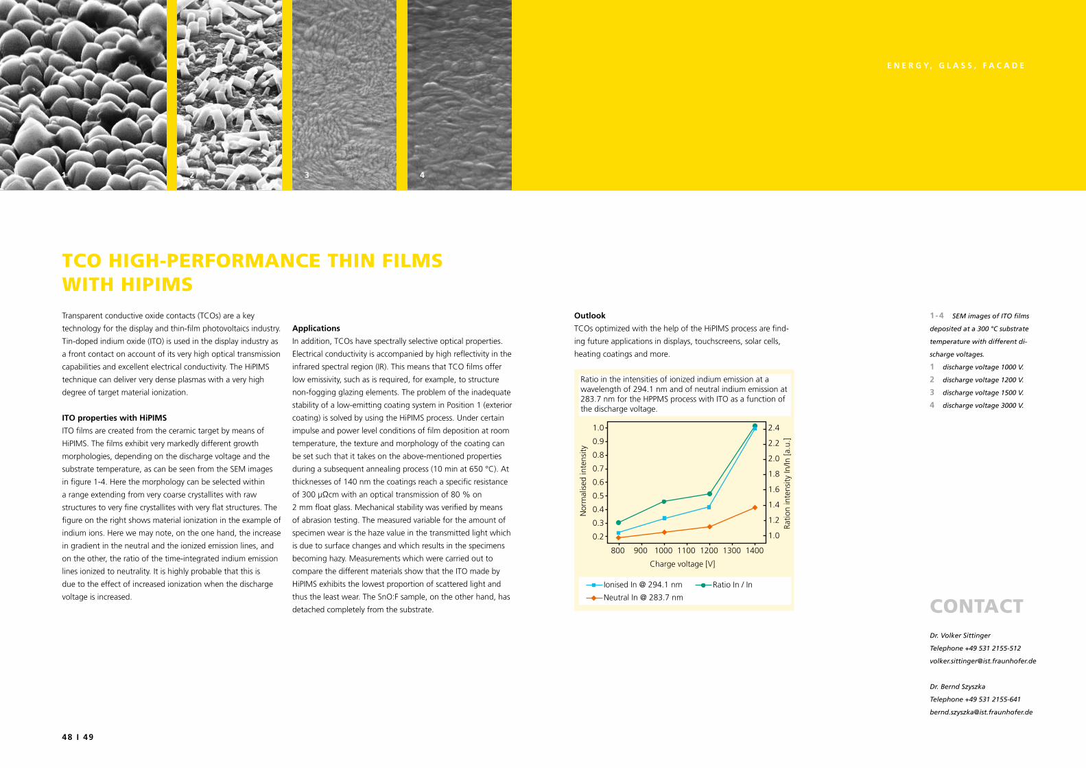
ITo properties with hipImS
ITO films are created from the ceramic target by means of
HiPIMS. The films exhibit very markedly different growth
morphologies, depending on the discharge voltage and the
substrate temperature, as can be seen from the SEM images
in figure 1-4. Here the morphology can be selected within
a range extending from very coarse crystallites with raw
structures to very fine crystallites with very flat structures. The
figure on the right shows material ionization in the example of
indium ions. Here we may note, on the one hand, the increase
in gradient in the neutral and the ionized emission lines, and
on the other, the ratio of the time-integrated indium emission
lines ionized to neutrality. It is highly probable that this is
due to the effect of increased ionization when the discharge
voltage is increased.
tco HigH-peRFoRmAnce tHin Films witH Hipims
1-4 SEM images of ITO films
deposited at a 300 °C substrate
temperature with different di-
scharge voltages.
1 discharge voltage 1000 V.
2 discharge voltage 1200 V.
3 discharge voltage 1500 V.
4 discharge voltage 3000 V.
42 31
contActDr. Volker Sittinger
Telephone +49 531 2155-512
Dr. Bernd Szyszka
Telephone +49 531 2155-641
Ratio
n in
tens
ity In
/In [a
.u.]
Nor
mal
ised
inte
nsity
Ratio in the intensities of ionized indium emission at a wavelength of 294.1 nm and of neutral indium emission at 283.7 nm for the HPPMS process with ITO as a function of the discharge voltage.
Charge voltage [V]
Ionised In @ 294.1 nm
Neutral In @ 283.7 nm
Ratio In / In
1.0
0.9
0.8
0.7
0.6
0.5
0.4
0.3
0.2
2.4
2.2
2.0
1.8
1.6
1.4
1.2
1.0
800 900 1000 1100 1200 1300 1400

50 I 51
o p T I C S , I n F o r m a T I o n , C o m m u n I C a T I o n
Topics falling within the business area “Optics, Information and Communication” include:
Developing coating systems for displays, Developing and designing multilayer coatings for optical filters, Metallizing plastics for 3D-MID and Developing new materials, structurizing and metallizing technologies to substitute ITO layer systems for flat panel display applications
Customers of this business area include the optical and automotive industries,
telecommunications, manufacturers of displays and data-storage as well as plant manufacturers
and contract coaters.
8 I 9
optics, inFoRmAtion, communicAtion
contActDr. Michael Vergöhl
Telephone + 49 531 2155-640
Dr. Ralf Bandorf
Telephone + 49 531 2155-602
52 I 53
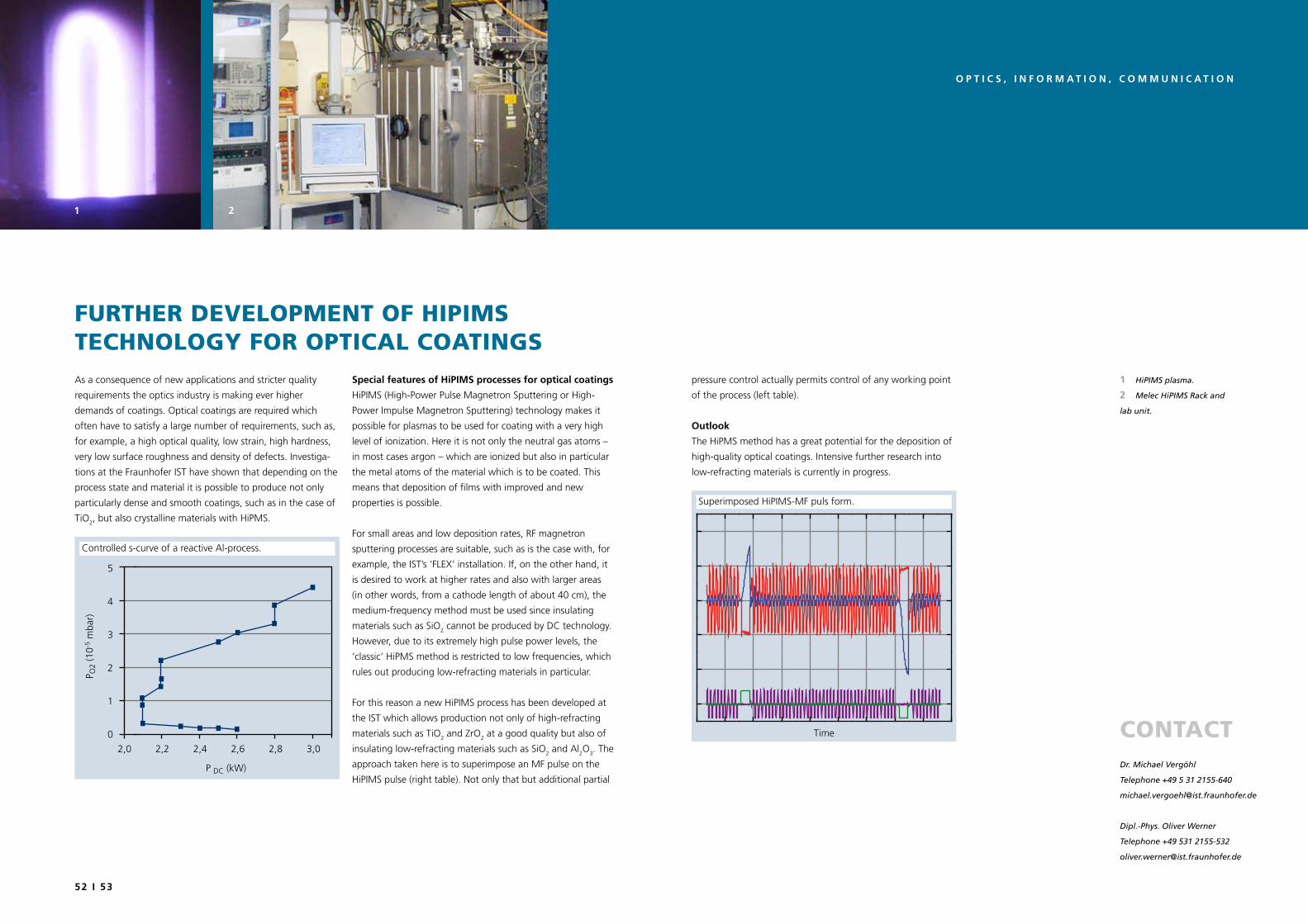
o p T I C S , I n F o r m a T I o n , C o m m u n I C a T I o n
Special features of hipImS processes for optical coatings
HiPIMS (High-Power Pulse Magnetron Sputtering or High-
Power Impulse Magnetron Sputtering) technology makes it
possible for plasmas to be used for coating with a very high
level of ionization. Here it is not only the neutral gas atoms –
in most cases argon – which are ionized but also in particular
the metal atoms of the material which is to be coated. This
means that deposition of films with improved and new
properties is possible.
For small areas and low deposition rates, RF magnetron
sputtering processes are suitable, such as is the case with, for
example, the IST’s ‘FLEX’ installation. If, on the other hand, it
is desired to work at higher rates and also with larger areas
(in other words, from a cathode length of about 40 cm), the
medium-frequency method must be used since insulating
materials such as SiO2 cannot be produced by DC technology.
However, due to its extremely high pulse power levels, the
‘classic’ HiPMS method is restricted to low frequencies, which
rules out producing low-refracting materials in particular.
For this reason a new HiPIMS process has been developed at
the IST which allows production not only of high-refracting
materials such as TiO2 and ZrO2 at a good quality but also of
insulating low-refracting materials such as SiO2 and Al2O3. The
approach taken here is to superimpose an MF pulse on the
HiPIMS pulse (right table). Not only that but additional partial
pressure control actually permits control of any working point
of the process (left table).
outlook
The HiPMS method has a great potential for the deposition of
high-quality optical coatings. Intensive further research into
low-refracting materials is currently in progress.
As a consequence of new applications and stricter quality
requirements the optics industry is making ever higher
demands of coatings. Optical coatings are required which
often have to satisfy a large number of requirements, such as,
for example, a high optical quality, low strain, high hardness,
very low surface roughness and density of defects. Investiga-
tions at the Fraunhofer IST have shown that depending on the
process state and material it is possible to produce not only
particularly dense and smooth coatings, such as in the case of
TiO2, but also crystalline materials with HiPMS.
FuRtHeR development oF Hipims tecHnologY FoR opticAl coAtings
1 HiPIMS plasma.
2 Melec HiPIMS Rack and
lab unit.
21
contActDr. Michael Vergöhl
Telephone +49 5 31 2155-640
Dipl.-Phys. Oliver Werner
Telephone +49 531 2155-532
Controlled s-curve of a reactive Al-process.
P O2
(10-5
mba
r)
P DC (kW)
5
4
3
2
1
02,0 2,2 2,4 2,6 2,8 3,0
Superimposed HiPIMS-MF puls form.
Time
54 I 55
o p T I C S , I n F o r m a T I o n , C o m m u n I C a T I o n
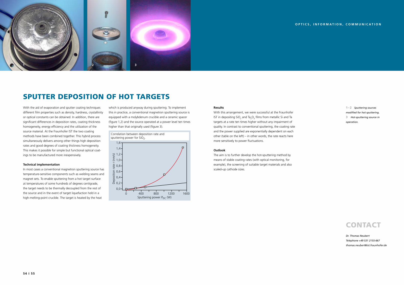
which is produced anyway during sputtering. To implement
this in practice, a conventional magnetron sputtering source is
equipped with a molybdenum crucible and a ceramic spacer
(figure 1,2) and the source operated at a power level ten times
higher than that originally used (figure 3).
results
With this arrangement, we were successful at the Fraunhofer
IST in depositing SiO2 and Ta2O5 films from metallic Si and Ta
targets at a rate ten times higher without any impairment of
quality. In contrast to conventional sputtering, the coating rate
and the power supplied are exponentially dependent on each
other (table on the left) – in other words, the rate reacts here
more sensitively to power fluctuations.
outlook
The aim is to further develop the hot-sputtering method by
means of stable coating rates (with optical monitoring, for
example), the screening of suitable target materials and also
scaled-up cathode sizes.
With the aid of evaporation and sputter coating techniques
different film properties such as density, hardness, crystallinity
or optical constants can be obtained. In addition, there are
significant differences in deposition rates, coating thickness
homogeneity, energy efficiency and the utilization of the
source material. At the Fraunhofer IST the two coating
methods have been combined together. This hybrid process
simultaneously delivers among other things high deposition
rates and good degrees of coating thickness homogeneity.
This makes it possible for simple but functional optical coat-
ings to be manufactured more inexpensively.
Technical implementation
In most cases a conventional magnetron sputtering source has
temperature-sensitive components such as welding seams and
magnet sets. To enable sputtering from a hot target surface
at temperatures of some hundreds of degrees centigrade,
the target needs to be thermally decoupled from the rest of
the source and in the event of target liquefaction held in a
high-melting-point crucible. The target is heated by the heat
sputteR deposition oF Hot tARgets1–2 Sputtering sources
modified for hot sputtering.
3 Hot-sputtering source in
operation.
2 31
contActDr. Thomas Neubert
Telephone +49 531 2155-667
Correlation between deposition rate and sputtering power for SiO2.
Dep
ositi
on r
ate
r (n
m/s
)
0,0
0,2
0,4
0,6
0,8
1,0
1,2
1,4
1,6
Sputtering power PDC (W)400 800 1200 16000
56 I 57
o p T I C S , I n F o r m a T I o n , C o m m u n I C a T I o n
Following these basic investigations, multilayer filter systems
were to be deposited by means of in-situ monitoring. Here
useful algorithms for compensating measuring errors were
developed and successfully tested. The table above shows the
theoretical calculated trajectories of the measured variables
(psi, delta) as a function of the film thickness. It was discovert
how successful and precisely the measurements could be
allocated to the theoretical calculations. To demonstrate the
full capability of the monitoring strategy a 23-layer bandpass
filter (cavity filter) was produced. The characteristic properties
of this filter matches those used in the fields of fluorescence
microscopy and telecommunications.
The goal was to achieve a transmission peak at 500 nm with
a very low half-width. With fully automated deposition a peak
was obtained at 499.09 nm with a half- width of less than a
nanometer (table below). This is up to a deviation in the layer-
thickness of the cavity layer of approx. 2 Ä.
outlook
The next step in development will be to incorporate a
broadband monitor in the existing control loop. The goal
is to develop a modular measurement system for industrial
applications.
As applications in the optics field become more and more
specialized, so are quality and precision requirements in the
optical coatings field. Due to its process-related advantages
and also the outstanding coating properties it delivers, mag-
netron sputtering has recently started being used more often
for manufacturing precision optics. In order to compensate for
short-term process fluctuations (drifts) which have negative
effects on the desired coating specifications, a new kind of
measuring procedure has been developed at the Fraunhofer
IST for in-situ monitoring of the deposition process.
approach
By means of monochromatic in-situ ellipsometry and monitor-
ing of measured variables, the relevant material parameters
(indices of refraction and absorption) and also the current de-
position rate can be determined. The process can be adjusted
on the basis of these results and its precision thus increased.
The route to success
Coating was carried out using the ‘Dyscus’ rotary platform sys-
tem which is equipped with a maximum of 3 twin magnetron
systems with a target length of 650 mm and a width of 125
mm. First of all a monochromatic ellipsometer was installed
on this system and a software application developed to model
and analyze the measured values and also to control the coat-
ing process. In this way the basic possibilities for measuring
layer thickness and determining the refractive index of Nb2O5
coatings on glass were investigated. It emerged that very exact
measurements were possible.
in-situ meAsuRement tecHniques FoR tHe optimizAtion oF dielectRic FilteRs
1 Dielectric filter.
1
contActDipl.-Phys. Daniel Rademacher
Telephone: +49 531 2155-674
Dr. Michael Vergöhl
Telephone: +49 531 2155-640
Theoretically calculated trajectories of the measurands (psi, delta) and the allocated in-situ measurements.
psi,
delta
[°]
Thickness [nm]
psi theoretical delta theoretical
psi measured delta measured
Layer 2 Layer 3Layer 1 Layer 4
0
40
80
120
160
0 40 0 50 100 0 40 0 50 100Transmission-Spectra of a narrowbanded band-pass filter that was produced using in-situ control. The goal was a transmission peak at 500 nm, a result of 499.09 nm at a half width of less than 1 nm was achieved.
496 498 500 502 5040
10
20
30
40
50
60
70
80
T<1%
~77%499,09 nm
Tran
smiss
ion
[%]
Wave length [nm]
0,98 nm
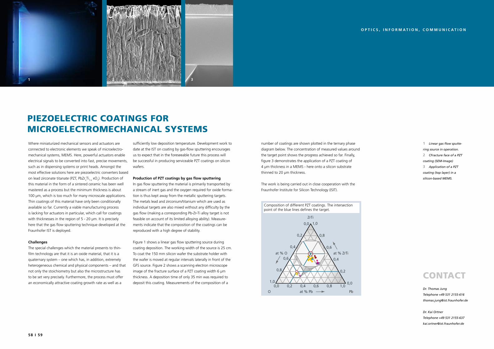
58 I 59
o p T I C S , I n F o r m a T I o n , C o m m u n I C a T I o n
sufficiently low deposition temperature. Development work to
date at the IST on coating by gas-flow sputtering encourages
us to expect that in the foreseeable future this process will
be successful in producing serviceable PZT coatings on silicon
wafers.
Production of PZT coatings by gas flow sputtering
In gas flow sputtering the material is primarily transported by
a stream of inert gas and the oxygen required for oxide forma-
tion is thus kept away from the metallic sputtering targets.
The metals lead and zirconium/titanium which are used as
individual targets are also mixed without any difficulty by the
gas flow (making a corresponding Pb-Zr-Ti alloy target is not
feasible on account of its limited alloying ability). Measure-
ments indicate that the composition of the coatings can be
reproduced with a high degree of stability.
Figure 1 shows a linear gas flow sputtering source during
coating deposition. The working width of the source is 25 cm.
To coat the 150 mm silicon wafer the substrate holder with
the wafer is moved at regular intervals laterally in front of the
GFS source. Figure 2 shows a scanning electron microscope
image of the fracture surface of a PZT coating width 6 µm
thickness. A deposition time of only 35 min was required to
deposit this coating. Measurements of the composition of a
number of coatings are shown plotted in the ternary phase
diagram below. The concentration of measured values around
the target point shows the progress achieved so far. Finally,
figure 3 demonstrates the application of a PZT coating of
4 µm thickness in a MEMS - here onto a silicon substrate
thinned to 20 µm thickness.
The work is being carried out in close cooperation with the
Fraunhofer Institute for Silicon Technology (ISIT).
Where miniaturized mechanical sensors and actuators are
connected to electronic elements we speak of microelectro-
mechanical systems, MEMS. Here, powerful actuators enable
electrical signals to be converted into fast, precise movements,
such as in dispensing systems or print heads. Amongst the
most effective solutions here are piezoelectric converters based
on lead zirconate titanate (PZT, PbZrxTi1-x xO3). Production of
this material in the form of a sintered ceramic has been well
mastered as a process but the minimum thickness is about
100 µm, which is too much for many microscale applications.
Thin coatings of this material have only been conditionally
available so far. Currently a viable manufacturing process
is lacking for actuators in particular, which call for coatings
with thicknesses in the region of 5 - 20 µm. It is precisely
here that the gas flow sputtering technique developed at the
Fraunhofer IST is deployed.
Challenges
The special challenges which the material presents to thin-
film technology are that it is an oxide material, that it is a
quaternary system – one which has, in addition, extremely
heterogeneous chemical and physical components – and that
not only the stoichiometry but also the microstructure has
to be set very precisely. Furthermore, the process must offer
an economically attractive coating growth rate as well as a
piezoelectRic coAtings FoR micRoelectRomecHAnicAl sYstems
1 Linear gas flow sputte-
ring source in operation.
2 CFracture face of a PZT
coating (SEM-Image)
3 Application of a PZT
coating (top layer) in a
silicon-based MEMS.
2 31
contActDr. Thomas Jung
Telephone +49 531 2155-616
Dr. Kai Ortner
Telephone +49 531 2155-637
Composition of different PZT coatings. The intersection point of the blue lines defines the target.
ZrTi
at % ZrTi
0,8
0,8
0,8
0,00,0
0,0
0,2
0,2
0,2
0,4
0,4
0,4 0,6
0,6
0,6
1,0
1,01,0
at % Pb
at % O
PbO
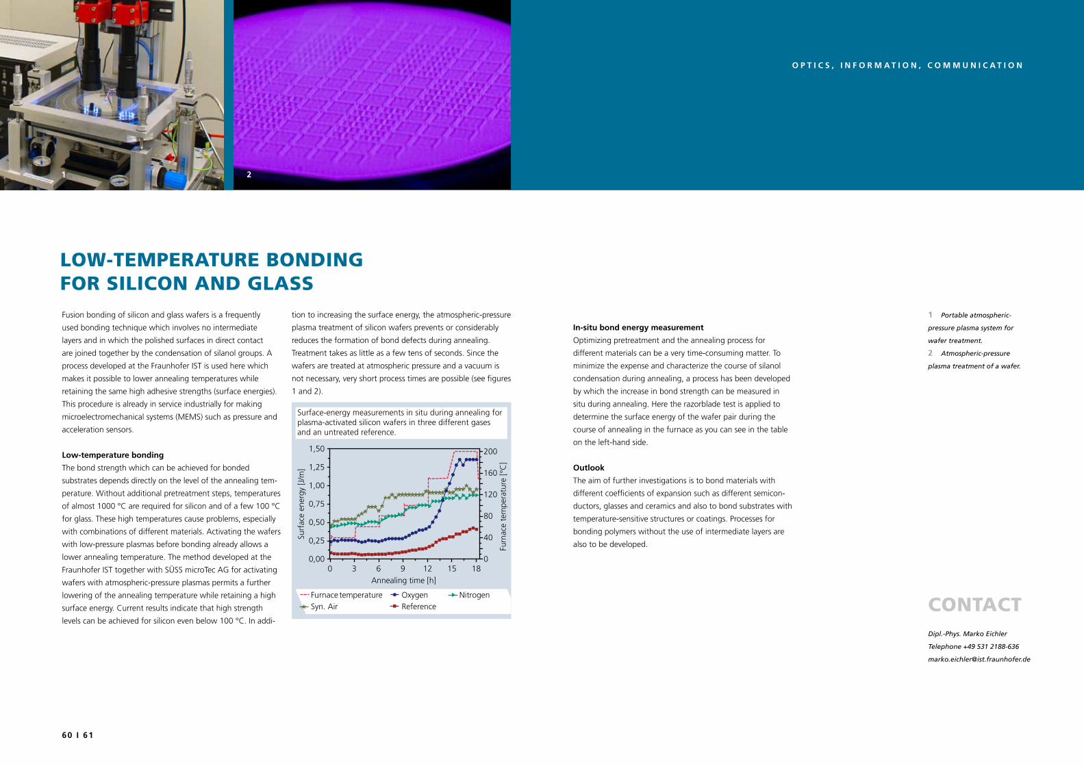
60 I 61
o p T I C S , I n F o r m a T I o n , C o m m u n I C a T I o n
tion to increasing the surface energy, the atmospheric-pressure
plasma treatment of silicon wafers prevents or considerably
reduces the formation of bond defects during annealing.
Treatment takes as little as a few tens of seconds. Since the
wafers are treated at atmospheric pressure and a vacuum is
not necessary, very short process times are possible (see figures
1 and 2).
In-situ bond energy measurement
Optimizing pretreatment and the annealing process for
different materials can be a very time-consuming matter. To
minimize the expense and characterize the course of silanol
condensation during annealing, a process has been developed
by which the increase in bond strength can be measured in
situ during annealing. Here the razorblade test is applied to
determine the surface energy of the wafer pair during the
course of annealing in the furnace as you can see in the table
on the left-hand side.
outlook
The aim of further investigations is to bond materials with
different coefficients of expansion such as different semicon-
ductors, glasses and ceramics and also to bond substrates with
temperature-sensitive structures or coatings. Processes for
bonding polymers without the use of intermediate layers are
also to be developed.
Fusion bonding of silicon and glass wafers is a frequently
used bonding technique which involves no intermediate
layers and in which the polished surfaces in direct contact
are joined together by the condensation of silanol groups. A
process developed at the Fraunhofer IST is used here which
makes it possible to lower annealing temperatures while
retaining the same high adhesive strengths (surface energies).
This procedure is already in service industrially for making
microelectromechanical systems (MEMS) such as pressure and
acceleration sensors.
low-temperature bonding
The bond strength which can be achieved for bonded
substrates depends directly on the level of the annealing tem-
perature. Without additional pretreatment steps, temperatures
of almost 1000 °C are required for silicon and of a few 100 °C
for glass. These high temperatures cause problems, especially
with combinations of different materials. Activating the wafers
with low-pressure plasmas before bonding already allows a
lower annealing temperature. The method developed at the
Fraunhofer IST together with SÜSS microTec AG for activating
wafers with atmospheric-pressure plasmas permits a further
lowering of the annealing temperature while retaining a high
surface energy. Current results indicate that high strength
levels can be achieved for silicon even below 100 °C. In addi-
low-tempeRAtuRe Bonding FoR silicon And glAss
1 Portable atmospheric-
pressure plasma system for
wafer treatment.
2 Atmospheric-pressure
plasma treatment of a wafer.
21
contActDipl.-Phys. Marko Eichler
Telephone +49 531 2188-636
Surface-energy measurements in situ during annealing for plasma-activated silicon wafers in three different gases and an untreated reference.
0 3 6 9 12 15 180,00
0,25
0,50
0,75
1,00
1,25
1,50
0
40
80
120
160
200
Surf
ace
ener
gy [J
/m]
Annealing time [h]
Furn
ace
tem
pera
ture
[°C
]
Furnace temperatureSyn. Air
OxygenReference
Nitrogen
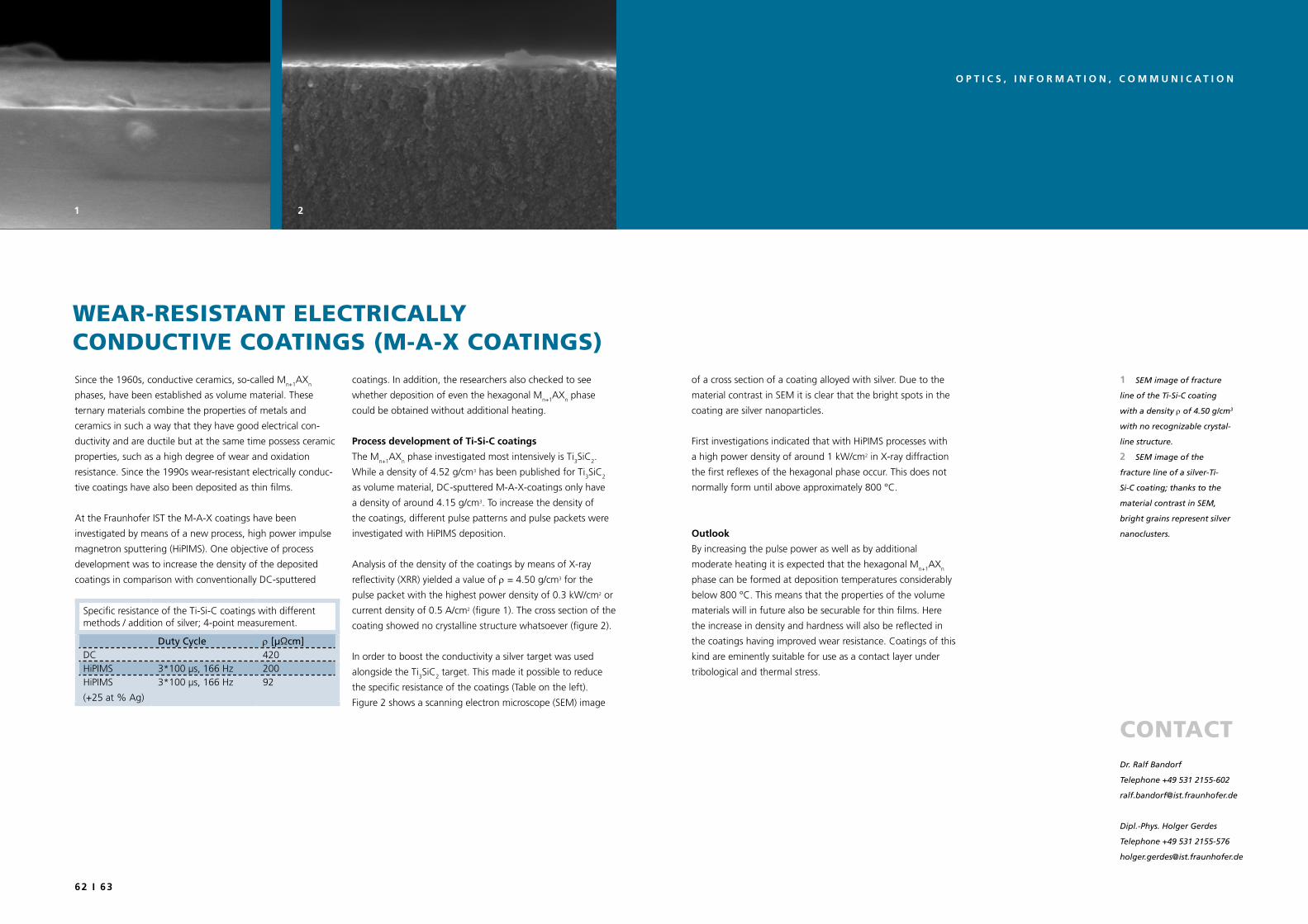
62 I 63
o p T I C S , I n F o r m a T I o n , C o m m u n I C a T I o n
coatings. In addition, the researchers also checked to see
whether deposition of even the hexagonal Mn+1AXn phase
could be obtained without additional heating.
process development of Ti-Si-C coatings
The Mn+1AXn phase investigated most intensively is Ti3SiC2.
While a density of 4.52 g/cm3 has been published for Ti3SiC2
as volume material, DC-sputtered M-A-X-coatings only have
a density of around 4.15 g/cm3. To increase the density of
the coatings, different pulse patterns and pulse packets were
investigated with HiPIMS deposition.
Analysis of the density of the coatings by means of X-ray
reflectivity (XRR) yielded a value of ρ = 4.50 g/cm3 for the
pulse packet with the highest power density of 0.3 kW/cm2 or
current density of 0.5 A/cm2 (figure 1). The cross section of the
coating showed no crystalline structure whatsoever (figure 2).
In order to boost the conductivity a silver target was used
alongside the Ti3SiC2 target. This made it possible to reduce
the specific resistance of the coatings (Table on the left).
Figure 2 shows a scanning electron microscope (SEM) image
of a cross section of a coating alloyed with silver. Due to the
material contrast in SEM it is clear that the bright spots in the
coating are silver nanoparticles.
First investigations indicated that with HiPIMS processes with
a high power density of around 1 kW/cm2 in X-ray diffraction
the first reflexes of the hexagonal phase occur. This does not
normally form until above approximately 800 °C.
outlook
By increasing the pulse power as well as by additional
moderate heating it is expected that the hexagonal Mn+1AXn
phase can be formed at deposition temperatures considerably
below 800 °C. This means that the properties of the volume
materials will in future also be securable for thin films. Here
the increase in density and hardness will also be reflected in
the coatings having improved wear resistance. Coatings of this
kind are eminently suitable for use as a contact layer under
tribological and thermal stress.
Since the 1960s, conductive ceramics, so-called Mn+1AXn
phases, have been established as volume material. These
ternary materials combine the properties of metals and
ceramics in such a way that they have good electrical con-
ductivity and are ductile but at the same time possess ceramic
properties, such as a high degree of wear and oxidation
resistance. Since the 1990s wear-resistant electrically conduc-
tive coatings have also been deposited as thin films.
At the Fraunhofer IST the M-A-X coatings have been
investigated by means of a new process, high power impulse
magnetron sputtering (HiPIMS). One objective of process
development was to increase the density of the deposited
coatings in comparison with conventionally DC-sputtered
weAR-ResistAnt electRicAllY conductive coAtings (m-A-x coAtings)
1 SEM image of fracture
line of the Ti-Si-C coating
with a density ρ of 4.50 g/cm3
with no recognizable crystal-
line structure.
2 SEM image of the
fracture line of a silver-Ti-
Si-C coating; thanks to the
material contrast in SEM,
bright grains represent silver
nanoclusters.
21
contActDr. Ralf Bandorf
Telephone +49 531 2155-602
Dipl.-Phys. Holger Gerdes
Telephone +49 531 2155-576
Specific resistance of the Ti-Si-C coatings with different methods / addition of silver; 4-point measurement.
Duty Cycle ρ [µΩcm]DC 420HiPIMS 3*100 µs, 166 Hz 200HiPIMS
(+25 at % Ag)
3*100 µs, 166 Hz 92
64 I 65
l I F e S C I e n C e a n D e C o l o G y
The focus of the business area ”Life Science and Ecology” is the development of surfaces for
applications in medical technology, biotechnology and environmental technology. Examples are:
Texturized functionalizing of surfaces for biochips or biosensors at atmospheric pressure Diamond coated electrodes for electrochemical disinfecting of water and treatment of waste water
Metal coating of plastic surfaces for biosensors Coating of interior surfaces in components for microfluidics, cell culture bags and plastic bottles
Friction-reducing biocompatible layers (i. e. diamond-like carbon layers) for medical applica- tions, i. e. implants
Our customers include the pharma ceuti cal-chemical industries, bio technology, medical technol-
ogy, food indus try, chemical industry and environmental technology.
8 I 9
liFe science And ecologY
contActDr. Simone Kondruweit
Telephone +49 531 2155-535
Prof. Dr. Claus-Peter Klages
Telephone +49 531 2155-510
Dr. Michael Thomas
Telephone +49 531 2155-525

66 I 67
l I F e S C I e n C e a n D e C o l o G y
outlook
Thin-film systems have been successfully built up on the basis
of a TiO2 layer which exhibit clear sensor properties with re-
spect to the very smallest quantities of oxygen. These systems
are manufactured by a very inexpensive process. The aim of
our efforts here is to develop an alternative to the established
lambda sensor.
Characterization of thin-film systems
Within a test chamber filled with 100 % nitrogen the sensor
chip is brought into direct contact with a small ceramic die
structured with platinum meander for heating up the sensor
layer system. After the heating phase a gas mixture consisting
of nitrogen and oxygen, with a minimum oxygen concentra-
tion of 50 ppm, is allowed to flow in and the change in sensor
resistance is simultaneously measured. After 20 minutes
100 % nitrogen is allowed to flow in again. This procedure is
continuously repeated with the oxygen content increased each
time by 50 ppm. The diagram to the right shows the results
of measurement. A characteristic rise in resistance of 5 MΩ is
to be measured with an oxygen content of 50 ppm and this
doubles each time the content doubles.
The typical operating temperatures of gas sensors lie between
350 and 1000 °C. Expanding their range of possible applica-
tions will require their operating temperature to be lowered
but without reducing their sensitivity. For this reason the
Fraunhofer IST is developing thin-film sensor systems with
operating temperatures between 150 °C and 250 °C.
Fabrication process
The thin-film system is built up on oxidized silicon wafers.
In the first step the wafer is coated homogeneously with
titanium dioxide by the magnetron sputtering process. Next,
this surface is photolithographically structured so that it is
entirely covered with photoresist but for the parts which
are to be metallized. The masked wafer is then coated with
chromium and after this with gold as an inert finish surface. In
the final step, the wafer is freed from the photoresist masking,
concluding the lift-off process. The interdigital structures are
left on the TiO2 layer. On its surface the wafer has a total of
112 structures (figure 1). In the final step the individual sensor
chips are cut out of the wafer (figure 2). It can be seen from
figure 1 that different designs of interdigital structure have
been made. Finger widths are typically between 100 μm and
200 µm as are the distances between the fingers. Each chip
measures 6 x 6 mm.
gAs sensoRs BAsed on titAnium dioxide FoR detecting oxYgen At low tempeRAtuRes
1 Silicon wafer with TiO2
based sensor structures.
2 Scattered sensor chips.
21
contActDipl.-Ing. Saskia Biehl
Telephone +49 531 2155-604
Fabrication of the thin-film sensor system.
Si-Wafer1
2
3
4
PVD-deposition of Cr-Au
Structured surface
Si-Wafer
Si-Wafer
Si-Wafer
Characteristic sensor behavior of the thin-film system in dependence on the oxygen concentration of gas mixture.
10
5
0
15
20
25
30
35
Resi
stan
ce [M
Ω]
0
50
100
150
200
250
Tem
pera
ture
[°C
]
0 50 100 150 200 250
Time [min]
250 ppm
200 ppm
150 ppm
100 ppm
50 ppm
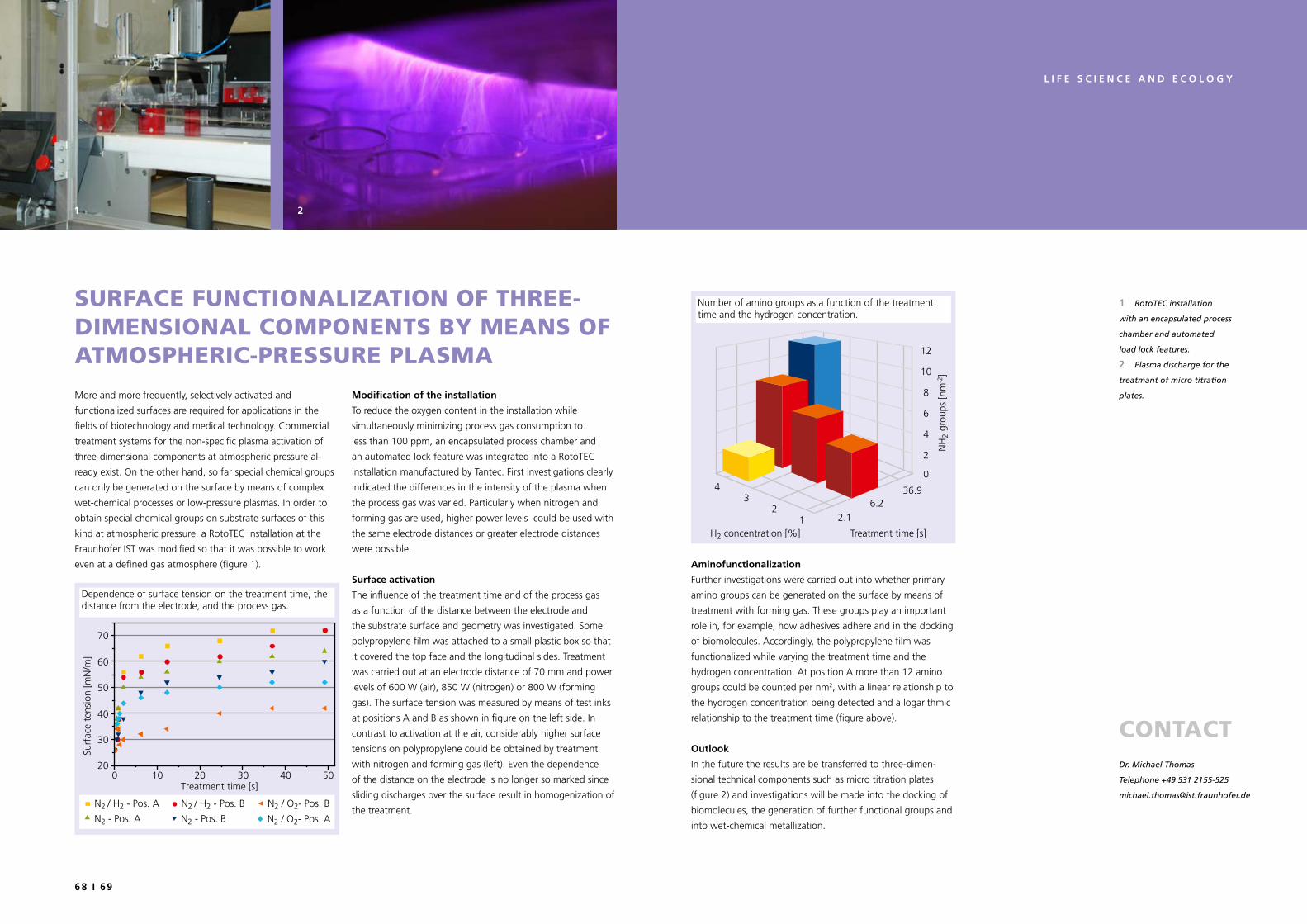
68 I 69
l I F e S C I e n C e a n D e C o l o G y
Modification of the installation
To reduce the oxygen content in the installation while
simultaneously minimizing process gas consumption to
less than 100 ppm, an encapsulated process chamber and
an automated lock feature was integrated into a RotoTEC
installation manufactured by Tantec. First investigations clearly
indicated the differences in the intensity of the plasma when
the process gas was varied. Particularly when nitrogen and
forming gas are used, higher power levels could be used with
the same electrode distances or greater electrode distances
were possible.
Surface activation
The influence of the treatment time and of the process gas
as a function of the distance between the electrode and
the substrate surface and geometry was investigated. Some
polypropylene film was attached to a small plastic box so that
it covered the top face and the longitudinal sides. Treatment
was carried out at an electrode distance of 70 mm and power
levels of 600 W (air), 850 W (nitrogen) or 800 W (forming
gas). The surface tension was measured by means of test inks
at positions A and B as shown in figure on the left side. In
contrast to activation at the air, considerably higher surface
tensions on polypropylene could be obtained by treatment
with nitrogen and forming gas (left). Even the dependence
of the distance on the electrode is no longer so marked since
sliding discharges over the surface result in homogenization of
the treatment.
aminofunctionalization
Further investigations were carried out into whether primary
amino groups can be generated on the surface by means of
treatment with forming gas. These groups play an important
role in, for example, how adhesives adhere and in the docking
of biomolecules. Accordingly, the polypropylene film was
functionalized while varying the treatment time and the
hydrogen concentration. At position A more than 12 amino
groups could be counted per nm2, with a linear relationship to
the hydrogen concentration being detected and a logarithmic
relationship to the treatment time (figure above).
outlook
In the future the results are be transferred to three-dimen-
sional technical components such as micro titration plates
(figure 2) and investigations will be made into the docking of
biomolecules, the generation of further functional groups and
into wet-chemical metallization.
More and more frequently, selectively activated and
functionalized surfaces are required for applications in the
fields of biotechnology and medical technology. Commercial
treatment systems for the non-specific plasma activation of
three-dimensional components at atmospheric pressure al-
ready exist. On the other hand, so far special chemical groups
can only be generated on the surface by means of complex
wet-chemical processes or low-pressure plasmas. In order to
obtain special chemical groups on substrate surfaces of this
kind at atmospheric pressure, a RotoTEC installation at the
Fraunhofer IST was modified so that it was possible to work
even at a defined gas atmosphere (figure 1).
suRFAce FunctionAlizAtion oF tHRee- dimensionAl components BY meAns oF AtmospHeRic-pRessuRe plAsmA
1 RotoTEC installation
with an encapsulated process
chamber and automated
load lock features.
2 Plasma discharge for the
treatmant of micro titration
plates.
21
contActDr. Michael Thomas
Telephone +49 531 2155-525
20
30
40
50
60
70
Surf
ace
tens
ion
[mN
/m]
0 10 20 30 40 50Treatment time [s]
Dependence of surface tension on the treatment time, the distance from the electrode, and the process gas.
N2 / H2 - Pos. A
N2 - Pos. A N2 / O2- Pos. A
N2 / H2 - Pos. B
N2 - Pos. B
N2 / O2- Pos. B
43
21
0
2
4
6
8
10
12
2.16.2
36.9
H2 concentration [%] Treatment time [s]
NH
2 gr
oups
[nm
-2]
Number of amino groups as a function of the treatment time and the hydrogen concentration.
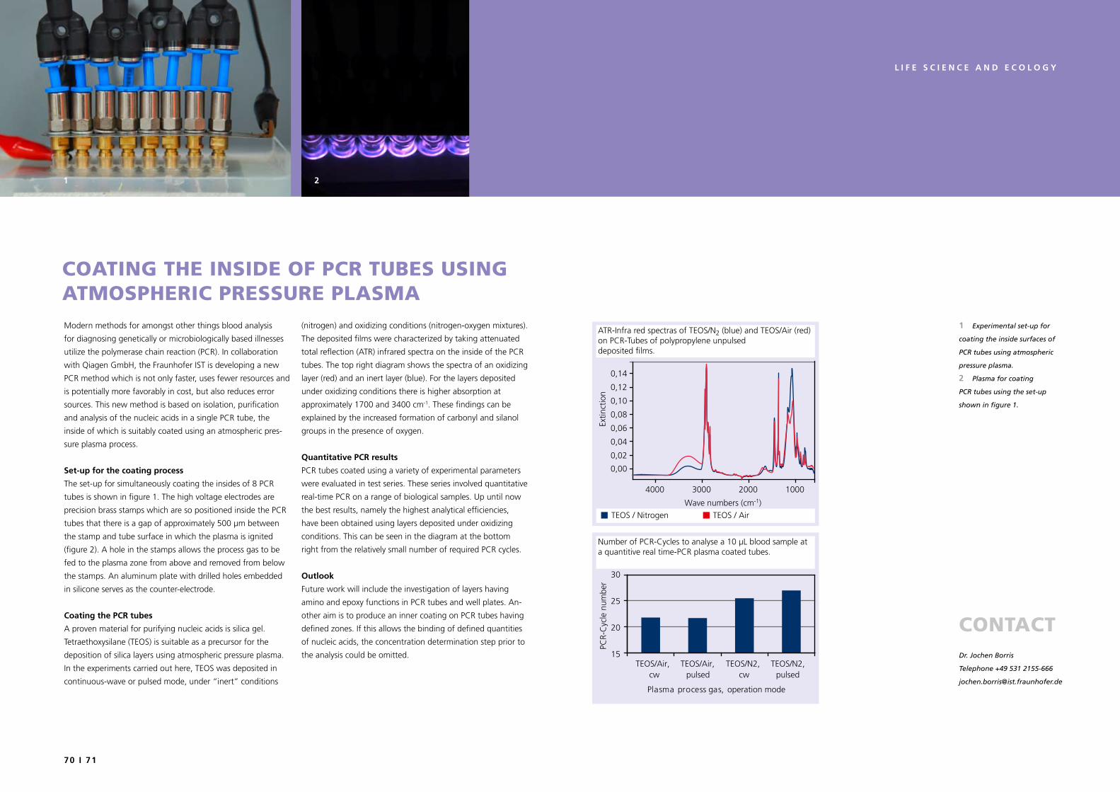
70 I 71
l I F e S C I e n C e a n D e C o l o G y
(nitrogen) and oxidizing conditions (nitrogen-oxygen mixtures).
The deposited films were characterized by taking attenuated
total reflection (ATR) infrared spectra on the inside of the PCR
tubes. The top right diagram shows the spectra of an oxidizing
layer (red) and an inert layer (blue). For the layers deposited
under oxidizing conditions there is higher absorption at
approximately 1700 and 3400 cm-1. These findings can be
explained by the increased formation of carbonyl and silanol
groups in the presence of oxygen.
Quantitative pCr results
PCR tubes coated using a variety of experimental parameters
were evaluated in test series. These series involved quantitative
real-time PCR on a range of biological samples. Up until now
the best results, namely the highest analytical efficiencies,
have been obtained using layers deposited under oxidizing
conditions. This can be seen in the diagram at the bottom
right from the relatively small number of required PCR cycles.
outlook
Future work will include the investigation of layers having
amino and epoxy functions in PCR tubes and well plates. An-
other aim is to produce an inner coating on PCR tubes having
defined zones. If this allows the binding of defined quantities
of nucleic acids, the concentration determination step prior to
the analysis could be omitted.
Modern methods for amongst other things blood analysis
for diagnosing genetically or microbiologically based illnesses
utilize the polymerase chain reaction (PCR). In collaboration
with Qiagen GmbH, the Fraunhofer IST is developing a new
PCR method which is not only faster, uses fewer resources and
is potentially more favorably in cost, but also reduces error
sources. This new method is based on isolation, purification
and analysis of the nucleic acids in a single PCR tube, the
inside of which is suitably coated using an atmospheric pres-
sure plasma process.
Set-up for the coating process
The set-up for simultaneously coating the insides of 8 PCR
tubes is shown in figure 1. The high voltage electrodes are
precision brass stamps which are so positioned inside the PCR
tubes that there is a gap of approximately 500 µm between
the stamp and tube surface in which the plasma is ignited
(figure 2). A hole in the stamps allows the process gas to be
fed to the plasma zone from above and removed from below
the stamps. An aluminum plate with drilled holes embedded
in silicone serves as the counter-electrode.
Coating the pCr tubes
A proven material for purifying nucleic acids is silica gel.
Tetraethoxysilane (TEOS) is suitable as a precursor for the
deposition of silica layers using atmospheric pressure plasma.
In the experiments carried out here, TEOS was deposited in
continuous-wave or pulsed mode, under “inert” conditions
coAting tHe inside oF pcR tuBes using AtmospHeRic pRessuRe plAsmA
1 Experimental set-up for
coating the inside surfaces of
PCR tubes using atmospheric
pressure plasma.
2 Plasma for coating
PCR tubes using the set-up
shown in figure 1.
1 2
contActDr. Jochen Borris
Telephone +49 531 2155-666
PCR-
Cyc
le n
umbe
r
Plasma process gas, operation mode
TEOS/Air,cw
TEOS/Air,pulsed
TEOS/N2,cw
TEOS/N2,pulsed
15
20
25
30
Number of PCR-Cycles to analyse a 10 µL blood sample at a quantitive real time-PCR plasma coated tubes.
ATR-Infra red spectras of TEOS/N2 (blue) and TEOS/Air (red) on PCR-Tubes of polypropylene unpulsed deposited films.
TEOS / Nitrogen TEOS / Air
Extin
ctio
n
Wave numbers (cm-1)
4000 3000 2000 1000
0,14
0,00
0,02
0,04
0,06
0,08
0,10
0,12
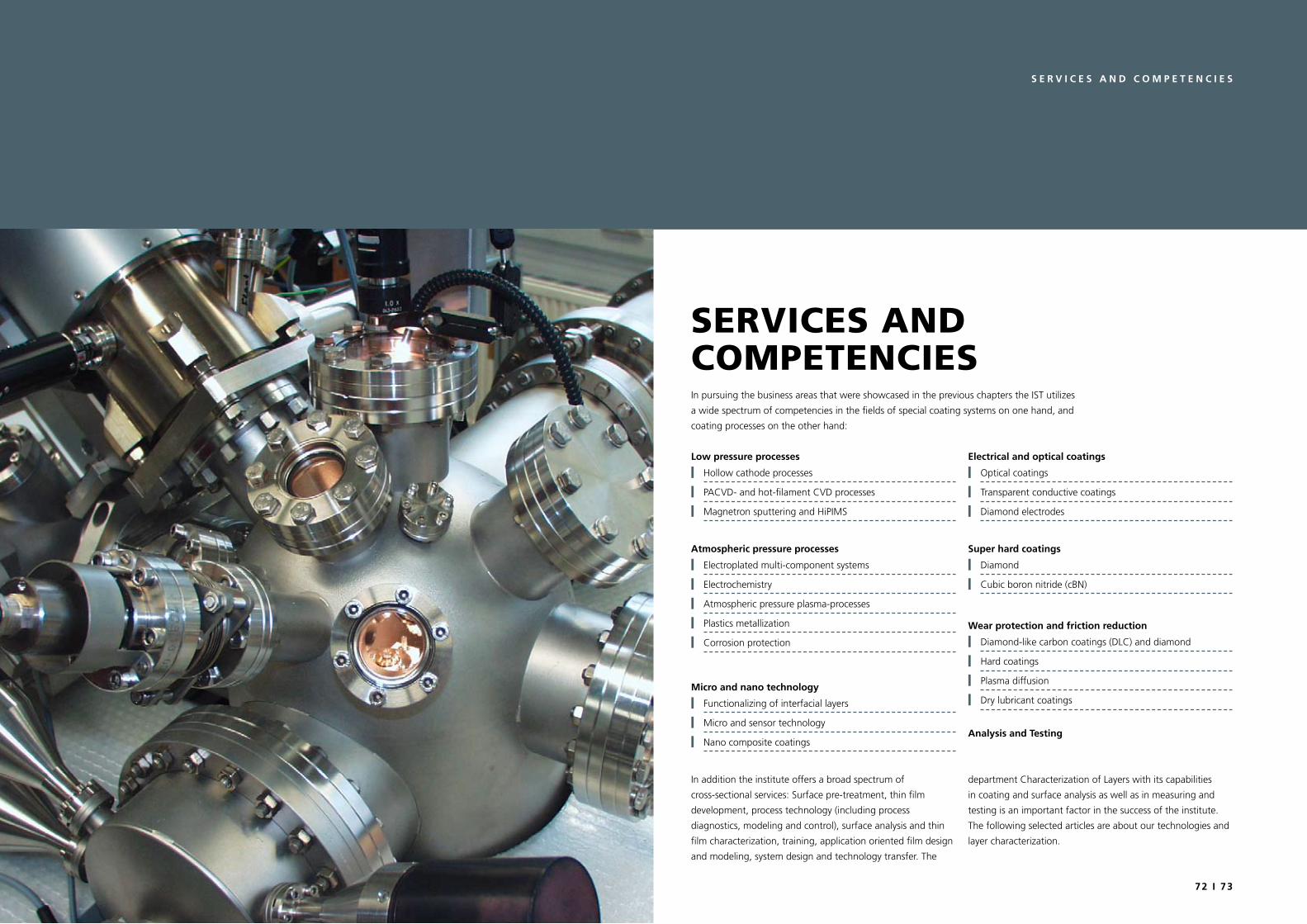
72 I 73
S e r v I C e S a n D C o m p e T e n C I e S
low pressure processes
Hollow cathode processes PACVD- and hot-filament CVD processes Magnetron sputtering and HiPIMS
atmospheric pressure processes
Electroplated multi-component systems Electrochemistry Atmospheric pressure plasma- processes Plastics metallization Corrosion protection
micro and nano technology
Functionalizing of interfacial layers Micro and sensor technology Nano composite coatings
In pursuing the business areas that were showcased in the previous chapters the IST utilizes
a wide spectrum of competencies in the fields of special coating systems on one hand, and
coating processes on the other hand:
In addition the institute offers a broad spectrum of
cross-sectional services: Surface pre-treatment, thin film
deve lopment, process technology (including process
diagnostics, modeling and control), surface analysis and thin
film characterization, training, application oriented film design
and modeling, system design and technology transfer. The
department Characterization of Layers with its capabilities
in coating and surface analysis as well as in measuring and
testing is an important factor in the success of the institute.
The following selected articles are about our technologies and
layer characterization.
electrical and optical coatings
Optical coatings Transparent conductive coatings Diamond electrodes
Super hard coatings
Diamond Cubic boron nitride (cBN)
wear protection and friction reduction
Diamond-like carbon coatings (DLC) and diamond Hard coatings Plasma diffusion Dry lubricant coatings
analysis and Testing
8 I 9
seRvices And competencies
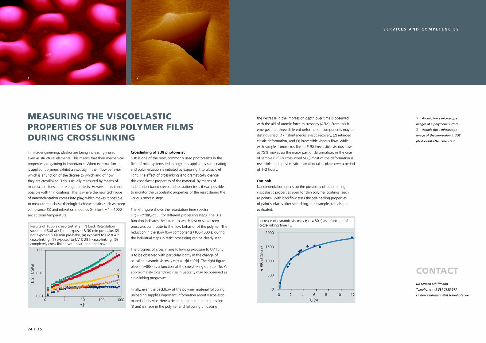
74 I 75
S e r v I C e S a n D C o m p e T e n C I e S
Crosslinking of Su8 photoresist
SU8 is one of the most commonly used photoresists in the
field of microsystems technology. It is applied by spin coating
and polymerization is initiated by exposing it to ultraviolet
light. The effect of crosslinking is to dramatically change
the viscoelastic properties of the material. By means of
indentation-based creep and relaxation tests it was possible
to monitor the viscoelastic properties of the resist during the
various process steps.
The left figure shows the retardation time spectra
L(τ) = -t*dJ(t)/dt |t=τ for different processing steps. The L(τ)
function indicates the extent to which fast or slow creep
processes contribute to the flow behavior of the polymer. The
reduction in the slow flow components (100-1000 s) during
the individual steps in resist processing can be clearly seen.
The progress of crosslinking following exposure to UV light
is to be observed with particular clarity in the change of
so-called dynamic viscosity η(t) = 1/[dJ(t)/dt]. The right figure
plots η(t=80s) as a function of the crosslinking duration Te. An
approximately logarithmic rise in viscosity may be observed as
crosslinking progresses.
Finally, even the backflow of the polymer material following
unloading supplies important information about viscoelastic
material behavior. Here a deep nanoindentation impression
(3 µm) is made in the polymer and following unloading
the decrease in the impression depth over time is observed
with the aid of atomic force microscopy (AFM). From this it
emerges that three different deformation components may be
distinguished: (1) instantaneous elastic recovery, (2) retarded
elastic deformation, and (3) irreversible viscous flow. While
with sample 1 (non-crosslinked SU8) irreversible viscous flow
at 75% makes up the major part of deformation, in the case
of sample 6 (fully crosslinked SU8) most of the deformation is
reversible and quasi-elastic relaxation takes place over a period
of 1–2 hours.
outlook
Nanoindentation opens up the possibility of determining
viscoelastic properties even for thin polymer coatings (such
as paints). With backflow tests the self-healing properties
of paint surfaces after scratching, for example, can also be
evaluated.
In microengineering, plastics are being increasingly used
even as structural elements. This means that their mechanical
properties are gaining in importance. When external force
is applied, polymers exhibit a viscosity in their flow behavior
which is a function of the degree to which and of how
they are crosslinked. This is usually measured by means of
macroscopic tension or elongation tests. However, this is not
possible with thin coatings. This is where the new technique
of nanoindentation comes into play, which makes it possible
to measure the classic rheological characteristics such as creep
compliance J(t) and relaxation modulus G(t) for t = 1 – 1000
sec at room temperature.
meAsuRing tHe viscoelAstic pRopeRties oF su8 polYmeR Films duRing cRosslinking
1 2
1 Atomic force microscope
images of a polymeric surface .
2 Atomic force microscope
image of the impression in SU8
photoresist after creep test.
contActDr. Kirsten Schiffmann
Telephone +49 531 2155-577
0,10
1,00
0 1 10 100 1000τ [s]
L (τ
) [1/
GPa
]
1 2
4
3
6
Results of 1000 s creep test at 2 mN load. Retardation spectra of SU8 at (1) not exposed & 30 min pre-bake, (2) not exposed & 60 min pre-bake, (4) exposed to UV & 4 h cross-linking, (3) exposed to UV & 29 h cross-linking, (6) completely cross-linked with post- and hard-bake.
Increase of dynamic viscosity η (t = 80 s) as a function of cross-linking time Te.
0 2 4 6 8 10 12
0
500
1000
1500
2000
Te (h)
η(8
0 s)
(GPa
s)
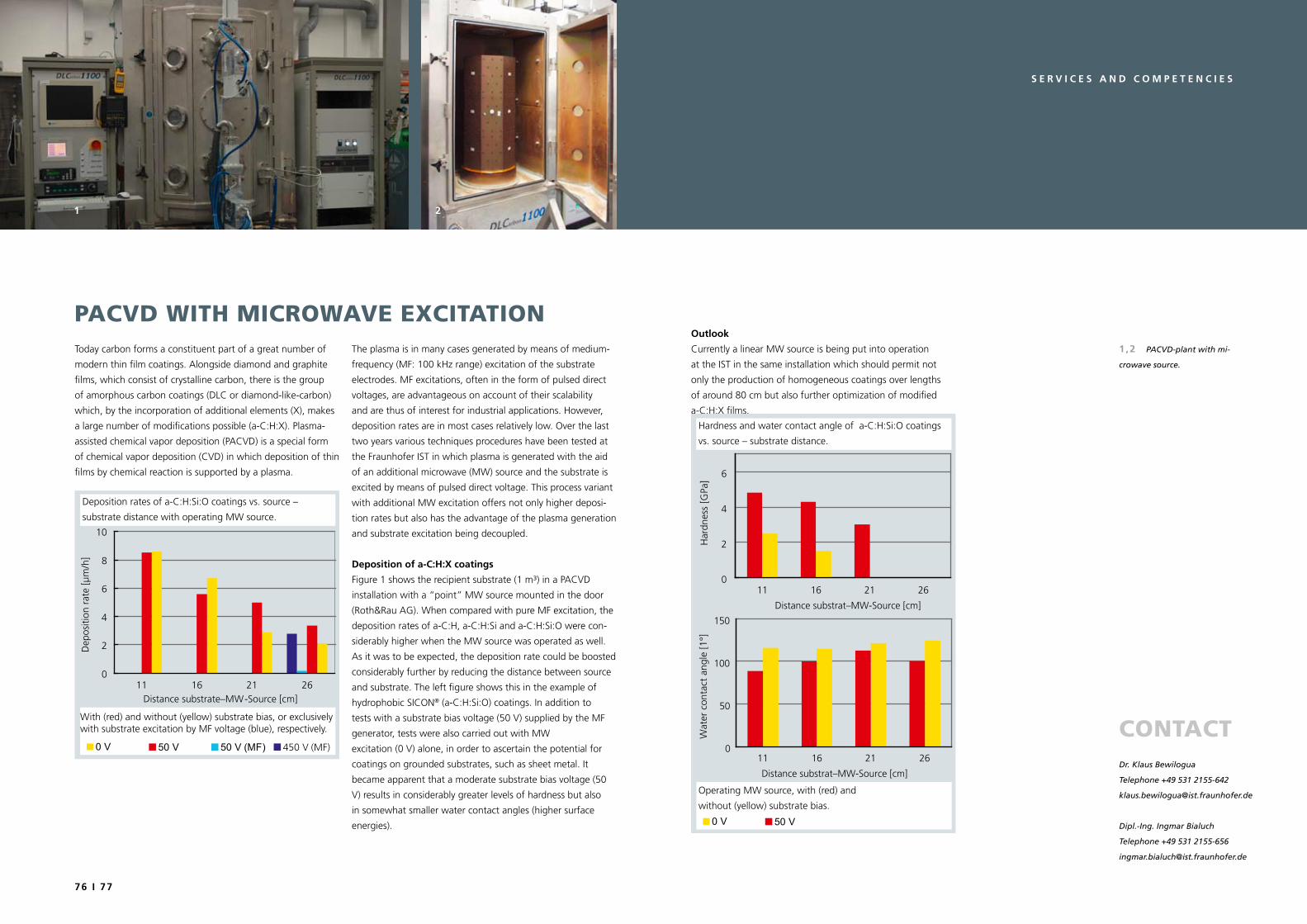
76 I 77
S e r v I C e S a n D C o m p e T e n C I e S
The plasma is in many cases generated by means of medium-
frequency (MF: 100 kHz range) excitation of the substrate
electrodes. MF excitations, often in the form of pulsed direct
voltages, are advantageous on account of their scalability
and are thus of interest for industrial applications. However,
deposition rates are in most cases relatively low. Over the last
two years various techniques procedures have been tested at
the Fraunhofer IST in which plasma is generated with the aid
of an additional microwave (MW) source and the substrate is
excited by means of pulsed direct voltage. This process variant
with additional MW excitation offers not only higher deposi-
tion rates but also has the advantage of the plasma generation
and substrate excitation being decoupled.
Deposition of a-C:h:X coatings
Figure 1 shows the recipient substrate (1 m³) in a PACVD
installation with a “point” MW source mounted in the door
(Roth&Rau AG). When compared with pure MF excitation, the
deposition rates of a-C:H, a-C:H:Si and a-C:H:Si:O were con-
siderably higher when the MW source was operated as well.
As it was to be expected, the deposition rate could be boosted
considerably further by reducing the distance between source
and substrate. The left figure shows this in the example of
hydrophobic SICON® (a-C:H:Si:O) coatings. In addition to
tests with a substrate bias voltage (50 V) supplied by the MF
generator, tests were also carried out with MW
excitation (0 V) alone, in order to ascertain the potential for
coatings on grounded substrates, such as sheet metal. It
became apparent that a moderate substrate bias voltage (50
V) results in considerably greater levels of hardness but also
in somewhat smaller water contact angles (higher surface
energies).
outlook
Currently a linear MW source is being put into operation
at the IST in the same installation which should permit not
only the production of homogeneous coatings over lengths
of around 80 cm but also further optimization of modified
a-C:H:X films.
Today carbon forms a constituent part of a great number of
modern thin film coatings. Alongside diamond and graphite
films, which consist of crystalline carbon, there is the group
of amorphous carbon coatings (DLC or diamond-like-carbon)
which, by the incorporation of additional elements (X), makes
a large number of modifications possible (a-C:H:X). Plasma-
assisted chemical vapor deposition (PACVD) is a special form
of chemical vapor deposition (CVD) in which deposition of thin
films by chemical reaction is supported by a plasma.
pAcvd witH micRowAve excitAtion
1 2
1,2 PACVD-plant with mi-
crowave source.
contActDr. Klaus Bewilogua
Telephone +49 531 2155-642
Dipl.-Ing. Ingmar Bialuch
Telephone +49 531 2155-656
Distance substrate–MW-Source [cm]
Dep
ositi
on r
ate
[µm
/h]
0
2
4
6
8
10
26211611
Deposition rates of a-C:H:Si:O coatings vs. source –
substrate distance with operating MW source.
With (red) and without (yellow) substrate bias, or exclusively with substrate excitation by MF voltage (blue), respectively.
450 V (MF)50 V (MF)50 V0 V
Wat
er c
onta
ct a
ngle
[1°]
Distance substrat–MW-Source [cm]
262116110
50
100
150
Har
dnes
s [G
Pa]
Distance substrat–MW-Source [cm]
262116110
2
4
6
50 V0 V
Hardness and water contact angle of a-C:H:Si:O coatings
vs. source – substrate distance.
Operating MW source, with (red) and
without (yellow) substrate bias.
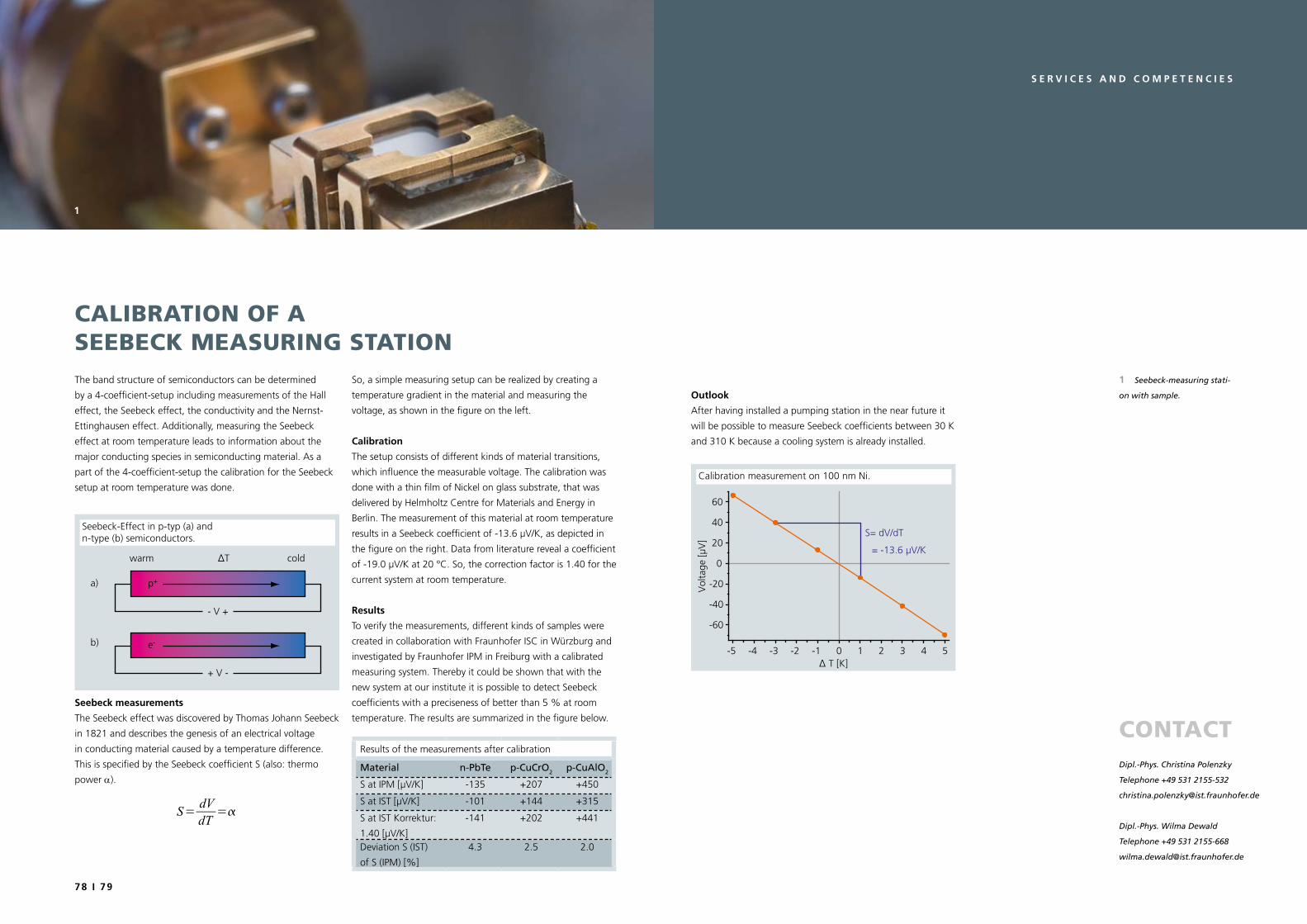
78 I 79
S e r v I C e S a n D C o m p e T e n C I e S
So, a simple measuring setup can be realized by creating a
temperature gradient in the material and measuring the
voltage, as shown in the figure on the left.
Calibration
The setup consists of different kinds of material transitions,
which influence the measurable voltage. The calibration was
done with a thin film of Nickel on glass substrate, that was
delivered by Helmholtz Centre for Materials and Energy in
Berlin. The measurement of this material at room temperature
results in a Seebeck coefficient of -13.6 µV/K, as depicted in
the figure on the right. Data from literature reveal a coefficient
of -19.0 µV/K at 20 °C. So, the correction factor is 1.40 for the
current system at room temperature.
results
To verify the measurements, different kinds of samples were
created in collaboration with Fraunhofer ISC in Würzburg and
investigated by Fraunhofer IPM in Freiburg with a calibrated
measuring system. Thereby it could be shown that with the
new system at our institute it is possible to detect Seebeck
coefficients with a preciseness of better than 5 % at room
temperature. The results are summarized in the figure below.
outlook
After having installed a pumping station in the near future it
will be possible to measure Seebeck coefficients between 30 K
and 310 K because a cooling system is already installed.
The band structure of semiconductors can be determined
by a 4-coefficient-setup including measurements of the Hall
effect, the Seebeck effect, the conductivity and the Nernst-
Ettinghausen effect. Additionally, measuring the Seebeck
effect at room temperature leads to information about the
major conducting species in semiconducting material. As a
part of the 4-coefficient-setup the calibration for the Seebeck
setup at room temperature was done.
Seebeck measurements
The Seebeck effect was discovered by Thomas Johann Seebeck
in 1821 and describes the genesis of an electrical voltage
in conducting material caused by a temperature difference.
This is specified by the Seebeck coefficient S (also: thermo
power α).
cAliBRAtion oF A seeBeck meAsuRing stAtion
1
1 Seebeck-measuring stati-
on with sample.
contActDipl.-Phys. Christina Polenzky
Telephone +49 531 2155-532
Dipl.-Phys. Wilma Dewald
Telephone +49 531 2155-668
Results of the measurements after calibration
Material n-PbTe p-CuCrO2 p-CuAlO2
S at IPM [µV/K] -135 +207 +450
S at IST [µV/K] -101 +144 +315
S at IST Korrektur:
1.40 [µV/K]
-141 +202 +441
Deviation S (IST)
of S (IPM) [%]
4.3 2.5 2.0
-5 -4 -3 -2 -1 0 1 2 3 4 5
-60
-40
-20
0
20
40
60
Vol
tage
[µV
]
∆ T [K]
S= dV/dT
= -13.6 µV/K
Calibration measurement on 100 nm Ni.
Seebeck-Effect in p-typ (a) and n-type (b) semiconductors.
warm ∆T
a)
b)
cold
p+
- V +
e-
+ V -

80 I 81
S e r v I C e S a n D C o m p e T e n C I e S
of kW/cm2 or peak current densities in the range of A/cm2 at
the target which result in very high ion concentrations. With
HiPIMS, coatings can thus be produced with a higher density,
hardness, wear resistance and so on which go far beyond
conventional coatings. In addition, the flow of material can
be controlled since the material forming the coating is for the
most part available in ionized form. This makes an improved
coating homogeneity possible with complex components.
Finally, coating types can be realized or structures created as
the coatings are deposited which until now have not been at
all possible with thin-film technology.
applications
HiPIMS technology can be used in all fields in which DC or MF
sputtering has been used. Upgrading existing coating systems
will be a straightforward matter since primarily the generators
need to be replaced or complemented by pulse power sup-
plies. However, some further additional steps will be required
for fine tuning. Currently a number of high power pulse
generators are commercially available. Furthermore, some
well known manufacturers of equipment are already offering
coating installations with the HiPIMS technology. In various
companies the corresponding pulse units are under evaluation
and the number of industrial processes using the new technol-
ogy is constantly rising. In the next ten years the changeover is
expected from academic research to a wide range of practical
applications.
1 Cost action MP0804:Hipp processes
High power impulse magnetron sputtering (HiPIMS, also
known as high power pulsed magnetron sputtering HPPMS)
is a new development of magnetron sputtering with a great
potential for practical use in all branches of industry. At the
Fraunhofer IST Dr. Ralf Bandorf has set up a European network
concerned with highly ionized pulsed plasma processes,
especially HiPIMS. In this field the IST has a unique position
worldwide. Four groups at Fraunhofer IST are working with
these new techniques in different fields of technology.
The technology
While the proportion of target ions in conventional magnetron
sputtering is just a few percent it can easily be increased by
pulsed operation. The degree of ionization of the sputtered
target material can amount to almost 100 % with HiPIMS. To
achieve this, HiPIMS applies very short pulses and long pauses
between them. With an input (mean) power comparable to
DC sputtering reached peak power densities are in the range
1 2
1 SEM-image of the break-
line of a DC-NiCr-deposit–
columnar growth.
2 SEM-image of the break-
line of a HiPIMS-NiCr-deposit
– glass-like structure.
contActDr. Ralf Bandorf
Telephone +49 531 2155-602
Dr. Volker Sittinger
Telephone +49 531 2155-512
Dr. Michael Vergöhl
Telephone +49 531 2155-640
tHe next geneRAtion oF sputteRing? HigH poweR impulse mAgnetRon sputteRing (Hipims/Hppms)
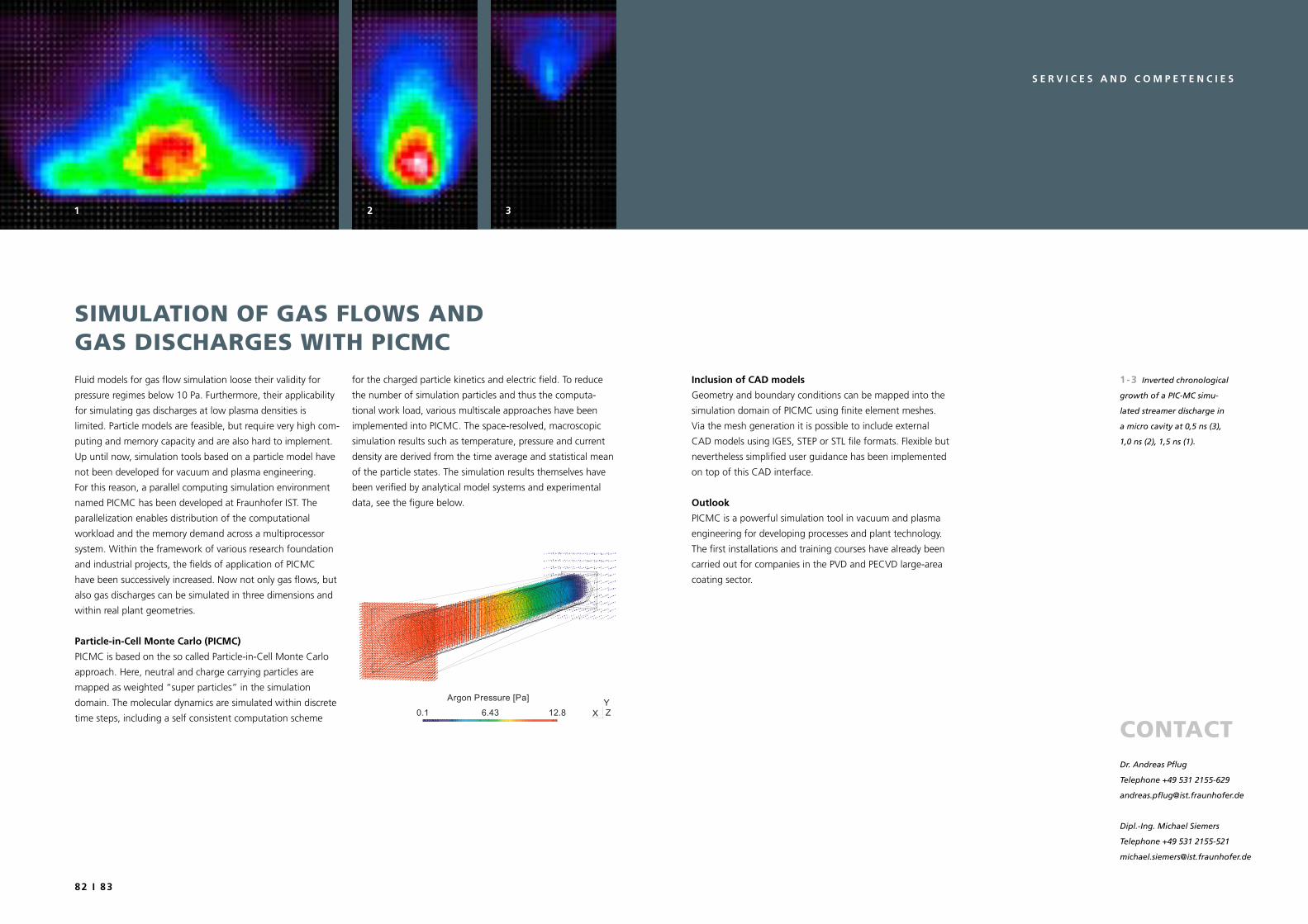
82 I 83
S e r v I C e S a n D C o m p e T e n C I e S
1
for the charged particle kinetics and electric field. To reduce
the number of simulation particles and thus the computa-
tional work load, various multiscale approaches have been
implemented into PICMC. The space-resolved, macroscopic
simulation results such as temperature, pressure and current
density are derived from the time average and statistical mean
of the particle states. The simulation results themselves have
been verified by analytical model systems and experimental
data, see the figure below.
Inclusion of CaD models
Geometry and boundary conditions can be mapped into the
simulation domain of PICMC using finite element meshes.
Via the mesh generation it is possible to include external
CAD models using IGES, STEP or STL file formats. Flexible but
nevertheless simplified user guidance has been implemented
on top of this CAD interface.
outlook
PICMC is a powerful simulation tool in vacuum and plasma
engineering for developing processes and plant technology.
The first installations and training courses have already been
carried out for companies in the PVD and PECVD large-area
coating sector.
Fluid models for gas flow simulation loose their validity for
pressure regimes below 10 Pa. Furthermore, their applicability
for simulating gas discharges at low plasma densities is
limited. Particle models are feasible, but require very high com-
puting and memory capacity and are also hard to implement.
Up until now, simulation tools based on a particle model have
not been developed for vacuum and plasma engineering.
For this reason, a parallel computing simulation environment
named PICMC has been developed at Fraunhofer IST. The
parallelization enables distribution of the computational
workload and the memory demand across a multiprocessor
system. Within the framework of various research foundation
and industrial projects, the fields of application of PICMC
have been successively increased. Now not only gas flows, but
also gas discharges can be simulated in three dimensions and
within real plant geometries.
particle-in-Cell monte Carlo (pICmC)
PICMC is based on the so called Particle-in-Cell Monte Carlo
approach. Here, neutral and charge carrying particles are
mapped as weighted “super particles” in the simulation
domain. The molecular dynamics are simulated within discrete
time steps, including a self consistent computation scheme
simulAtion oF gAs Flows And gAs discHARges witH picmc
1-3 Inverted chronological
growth of a PIC-MC simu-
lated streamer discharge in
a micro cavity at 0,5 ns (3),
1,0 ns (2), 1,5 ns (1).
2 3
contActDr. Andreas Pflug
Telephone +49 531 2155-629
Dipl.-Ing. Michael Siemers
Telephone +49 531 2155-521
0.1 6.43 12.8
Argon Pressure [Pa] YX Z
84 I 85
S e r v I C e S a n D C o m p e T e n C I e S
FIelD oF aCTIon 3:
production technology with high performance processes
TheSIS 5 The innovative potential of functional surfaces can only be exploited by transferring new kinds of coating and structuring techniques into industrial volume production.
TheSIS 6 Substantial improvements in material develop-ment, plant optimization and production are achieved by combining different simulation models. In particular, the combining of material and process models on different large scales leads to the optimization of complex production processes.
TheSIS 7 Optimum control of complex processes is only possible by combining models, simulation and analytical technology. For precise monitoring of high performance processes, favorable-cost, in-line measurement systems suitable for industry are required.
Surface technology is a key and a cross-sector technology for
virtually all sectors of industry: From machine construction,
the automotive sector, aviation and aerospace to the optical
industry, energy sector and medical engineering. In order
to appraise the current status of production technology for
functional surfaces and to assess the research needs and
future perspectives, a study was carried out by the Fraunhofer
Institute for Surface Engineering and Thin Films IST in con-
junction with the Fraunhofer Institute for Production Technol-
ogy and Automation IPA and the Fraunhofer Institute for
Material and Beam Technology IWS. The topic of this survey
was “Production technology for the gerneration of functional
surfaces”. Many of the findings were used for the project
tender document “Research for future production in the area
of resource efficiency” and are summarized in a report which
can be downloaded from www.ist.fraunhofer.de.
Within the survey, three fields of action were identified and
seven theses were derived:
FIelD oF aCTIon 1:
Energy and resource efficiency in product
and process
TheSIS 1 In order to safeguard and strengthen Germany’s international position in the marketplace, it is inevitable that there must be an increase in the energy and resource efficiency of production technology. In order to in-crease competitiveness in global markets, the full potential of functional surfaces must be utilized, with regards to both their manufacture and application.
TheSIS 2 By using products with functional surfaces, resources can be saved over the total lifetime. This is best achieved by an early and holistic consideration of the op-tions and characteristics during product development.
pRoduction tecHnologY FoR tHe geneRAtion oF FunctionAl suRFAces – stAtus And peRspectives
FIelD oF aCTIon 2:
production-integrated generation of functional surfaces
TheSIS 3 Highly integrated processes are the precondi-tion for seamless integration of surface functionalization in production sequences. Due to the shifting of process boundaries and due to the increased process intensification there are opportunities for new materials and new fields of application.
TheSIS 4 Optimum energy and resource usage for technically demanding films or structures can often best be achieved using a combination of different techniques. In particular, unusual combinations may offer entire new opportunities.
contActDipl.-Ing. Wolfgang Diehl
Telephone +49 531 2155-515
86 I 87
S e r v I C e S a n D C o m p e T e n C I e S
There are a lot of nationally protected inventions in plasma
technology but who lodged the patent applications? in which
research fields are they concentrated? and, above all, who
are the leading companies? Scientists at the Fraunhofer IST
tackled these questions in 2008 and summarized the answers
to make them generally accessible.
Patents are the measure of the innovative power of a company
or research institute. However, information about who made
application for what patent in recent years is rare. Data are
available in different databases with no links to each other
but specific information about plasma patents is hard to filter
out. In collaboration with the Fraunhofer Society and in close
contact with the inventors, Reinhold Bethke, an engineer at
the Fraunhofer IST, has developed the first patent database for
plasma technology.
FRAunHoFeR ist sets up tHe FiRst inteRnAtionAl pAtent dAtABAse FoR plAsmA tecHnologY
information, such as name, number, technical classification
(by process, for example), company rankings, geographical
distribution and origin of the patent, but also qualitative
results. Patent studies focusing on specific thematic fields are
offered separately. “These often represent important sources
of information for companies who wish to use new technolo-
gies”, explains Reinhold Bethke. Especially positive indeed: the
world’s first publicly accessible analysis of international patent
applications revealed that the Fraunhofer-Gesellschaft is
globally the foremost research institute in the case of patents
in plasma technology.
outlook
The service platform for international patents in plasma
technology is be launched in 2009 at the Hannover Fair.
More than 20,000 patent families are already included in the
database and the number is growing. All data are updated at
regular intervals. Subdivided into these categories
Coating deposition Surface modification Etching Properties of plasma
they can be particularized as desired as regards their
information content. The result - as diagrams, text or expert
statements - bring transparency into the plasma landscape.
The group at which this new service is aimed is companies or
research institutes who wish to avoid researching in the wrong
direction. The database supplies not only purely quantitative
contActDipl.-Ing. Reinhold Bethke
Telephone +49 531 2155-624
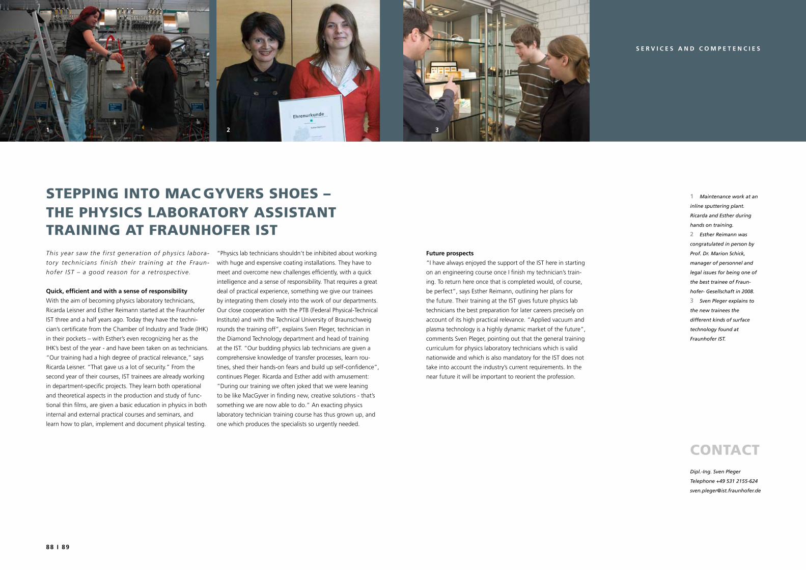
88 I 89
S e r v I C e S a n D C o m p e T e n C I e S
This year saw the f i rst generat ion of phys ics labora-
tory technic ians f in ish their t ra in ing at the Fraun-
hofer IST – a good reason for a retrospect ive.
Quick, efficient and with a sense of responsibility
With the aim of becoming physics laboratory technicians,
Ricarda Leisner and Esther Reimann started at the Fraunhofer
IST three and a half years ago. Today they have the techni-
cian’s certificate from the Chamber of Industry and Trade (IHK)
in their pockets – with Esther’s even recognizing her as the
IHK’s best of the year - and have been taken on as technicians.
“Our training had a high degree of practical relevance,” says
Ricarda Leisner. “That gave us a lot of security.” From the
second year of their courses, IST trainees are already working
in department-specific projects. They learn both operational
and theoretical aspects in the production and study of func-
tional thin films, are given a basic education in physics in both
internal and external practical courses and seminars, and
learn how to plan, implement and document physical testing.
“Physics lab technicians shouldn’t be inhibited about working
with huge and expensive coating installations. They have to
meet and overcome new challenges efficiently, with a quick
intelligence and a sense of responsibility. That requires a great
deal of practical experience, something we give our trainees
by integrating them closely into the work of our departments.
Our close cooperation with the PTB (Federal Physical-Technical
Institute) and with the Technical University of Braunschweig
rounds the training off”, explains Sven Pleger, technician in
the Diamond Technology department and head of training
at the IST. “Our budding physics lab technicians are given a
comprehensive knowledge of transfer processes, learn rou-
tines, shed their hands-on fears and build up self-confidence”,
continues Pleger. Ricarda and Esther add with amusement:
“During our training we often joked that we were leaning
to be like MacGyver in finding new, creative solutions - that’s
something we are now able to do.” An exacting physics
laboratory technician training course has thus grown up, and
one which produces the specialists so urgently needed.
Future prospects
“I have always enjoyed the support of the IST here in starting
on an engineering course once I finish my technician’s train-
ing. To return here once that is completed would, of course,
be perfect”, says Esther Reimann, outlining her plans for
the future. Their training at the IST gives future physics lab
technicians the best preparation for later careers precisely on
account of its high practical relevance. “Applied vacuum and
plasma technology is a highly dynamic market of the future”,
comments Sven Pleger, pointing out that the general training
curriculum for physics laboratory technicians which is valid
nationwide and which is also mandatory for the IST does not
take into account the industry’s current requirements. In the
near future it will be important to reorient the profession.
stepping into mAc gYveRs sHoes –tHe pHYsics lABoRAtoRY AssistAnt tRAining At FRAunHoFeR ist
contActDipl.-Ing. Sven Pleger
Telephone +49 531 2155-624
1 Maintenance work at an
inline sputtering plant.
Ricarda and Esther during
hands on training.
2 Esther Reimann was
congratulated in person by
Prof. Dr. Marion Schick,
manager of personnel and
legal issues for being one of
the best trainee of Fraun-
hofer- Gesellschaft in 2008.
3 Sven Pleger explains to
the new trainees the
different kinds of surface
technology found at
Fraunhofer IST.
1 2 3

90 I 91
n a m e S , D a T e S , e v e n T S 2 0 0 8
In 2008 the Fraunhofer IST once again presented its work and research results on a variety of
platforms. Below you will find an overview of the most important events and activities which
took place in 2008.
Fairs and conferences Workshops Exhibitions and institute visits Foreign trips Involvement in official bodies Prizes and awards
nAmes, dAtes, events 2008
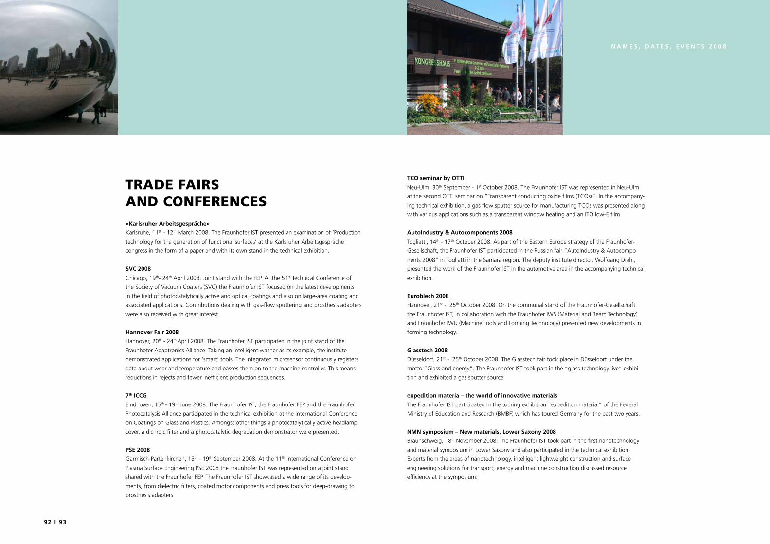
92 I 93
n a m e S , D a T e S , e v e n T S 2 0 0 8
tRAde FAiRs And conFeRences»karlsruher arbeitsgespräche«
Karlsruhe, 11th - 12th March 2008. The Fraunhofer IST presented an examination of ‘Production
technology for the generation of functional surfaces’ at the Karlsruher Arbeitsgespräche
congress in the form of a paper and with its own stand in the technical exhibition.
SvC 2008
Chicago, 19th- 24th April 2008. Joint stand with the FEP. At the 51st Technical Conference of
the Society of Vacuum Coaters (SVC) the Fraunhofer IST focused on the latest developments
in the field of photocatalytically active and optical coatings and also on large-area coating and
associated applications. Contributions dealing with gas-flow sputtering and prosthesis adapters
were also received with great interest.
hannover Fair 2008
Hannover, 20th - 24th April 2008. The Fraunhofer IST participated in the joint stand of the
Fraunhofer Adaptronics Alliance. Taking an intelligent washer as its example, the institute
demonstrated applications for ‘smart’ tools. The integrated microsensor continuously registers
data about wear and temperature and passes them on to the machine controller. This means
reductions in rejects and fewer inefficient production sequences.
7th ICCG
Eindhoven, 15th - 19th June 2008. The Fraunhofer IST, the Fraunhofer FEP and the Fraunhofer
Photocatalysis Alliance participated in the technical exhibition at the International Conference
on Coatings on Glass and Plastics. Amongst other things a photocatalytically active headlamp
cover, a dichroic filter and a photocatalytic degradation demonstrator were presented.
pSe 2008
Garmisch-Partenkirchen, 15th - 19th September 2008. At the 11th International Conference on
Plasma Surface Engineering PSE 2008 the Fraunhofer IST was represented on a joint stand
shared with the Fraunhofer FEP. The Fraunhofer IST showcased a wide range of its develop-
ments, from dielectric filters, coated motor components and press tools for deep-drawing to
prosthesis adapters.
TCo seminar by oTTI
Neu-Ulm, 30th September - 1st October 2008. The Fraunhofer IST was represented in Neu-Ulm
at the second OTTI seminar on “Transparent conducting oxide films (TCOs)”. In the accompany-
ing technical exhibition, a gas flow sputter source for manufacturing TCOs was presented along
with various applications such as a transparent window heating and an ITO low-E film.
autoIndustry & autocomponents 2008
Togliatti, 14th - 17th October 2008. As part of the Eastern Europe strategy of the Fraunhofer-
Gesellschaft, the Fraunhofer IST participated in the Russian fair “AutoIndustry & Autocompo-
nents 2008” in Togliatti in the Samara region. The deputy institute director, Wolfgang Diehl,
presented the work of the Fraunhofer IST in the automotive area in the accompanying technical
exhibition.
euroblech 2008
Hannover, 21st - 25th October 2008. On the communal stand of the Fraunhofer-Gesellschaft
the Fraunhofer IST, in collaboration with the Fraunhofer IWS (Material and Beam Technology)
and Fraunhofer IWU (Machine Tools and Forming Technology) presented new developments in
forming technology.
Glasstech 2008
Düsseldorf, 21st - 25th October 2008. The Glasstech fair took place in Düsseldorf under the
motto “Glass and energy”. The Fraunhofer IST took part in the “glass technology live” exhibi-
tion and exhibited a gas sputter source.
expedition materia – the world of innovative materials
The Fraunhofer IST participated in the touring exhibition “expedition material” of the Federal
Ministry of Education and Research (BMBF) which has toured Germany for the past two years.
nmn symposium – new materials, lower Saxony 2008
Braunschweig, 18th November 2008. The Fraunhofer IST took part in the first nanotechnology
and material symposium in Lower Saxony and also participated in the technical exhibition.
Experts from the areas of nanotechnology, intelligent lightweight construction and surface
engineering solutions for transport, energy and machine construction discussed resource
efficiency at the symposium.
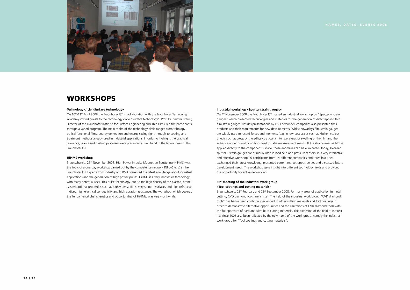
94 I 95
n a m e S , D a T e S , e v e n T S 2 0 0 8
woRksHopsTechnology circle »Surface technology«
On 10th-11th April 2008 the Fraunhofer IST in collaboration with the Fraunhofer Technology
Academy invited guests to the technology circle “Surface technology”. Prof. Dr. Günter Bräuer,
Director of the Fraunhofer Institute for Surface Engineering and Thin Films, led the participants
through a varied program. The main topics of the technology circle ranged from tribology,
optical functional films, energy generation and energy saving right through to coating and
treatment methods already used in industrial applications. In order to highlight the practical
relevance, plants and coating processes were presented at first hand in the laboratories of the
Fraunhofer IST.
hipImS workshop
Braunschweig, 26th November 2008. High Power Impulse Magnetron Sputtering (HiPIMS) was
the topic of a one-day workshop carried out by the competence network INPLAS e. V. at the
Fraunhofer IST. Experts from industry and R&D presented the latest knowledge about industrial
applications and the generation of high power pulses. HiPIMS is a very innovative technology
with many potential uses. This pulse technology, due to the high density of the plasma, prom-
ises exceptional properties such as highly dense films, very smooth surfaces and high refractive
indices, high electrical conductivity and high abrasion resistance. The workshop, which covered
the fundamental characteristics and opportunities of HiPIMS, was very worthwhile.
Industrial workshop »Sputter-strain gauges«
On 4th November 2008 the Fraunhofer IST hosted an industrial workshop on “Sputter – strain
gauges” which presented technologies and materials for the generation of direct applied thin
film strain gauges. Besides presentations by R&D personnel, companies also presented their
products and their requirements for new developments. Whilst nowadays film strain gauges
are widely used to record forces and moments (e.g. in low-cost scales such as kitchen scales),
effects such as creep of the adhesive at certain temperatures or swelling of the film and the
adhesive under humid conditions lead to false measurement results. If the strain-sensitive film is
applied directly to the component surface, these anomalies can be eliminated. Today, so-called
sputter – strain gauges are primarily used in load cells and pressure sensors. In a very interactive
and effective workshop 40 participants from 14 different companies and three institutes
exchanged their latest knowledge, presented current market opportunities and discussed future
development needs. The workshop gave insight into different technology fields and provided
the opportunity for active networking.
18th meeting of the industrial work group
»Tool coatings and cutting materials«
Braunschweig, 28th February and 23rd September 2008. For many areas of application in metal
cutting, CVD diamond tools are a must. The field of the industrial work group “CVD diamond
tools” has hence been continually extended to other cutting materials and tool coatings in
order to demonstrate alternative opportunities and the limitations of CVD diamond tools with
the full spectrum of hard and ultra hard cutting materials. This extension of the field of interest
has since 2008 also been reflected by the new name of the work group, namely the industrial
work group for “Tool coatings and cutting materials”.
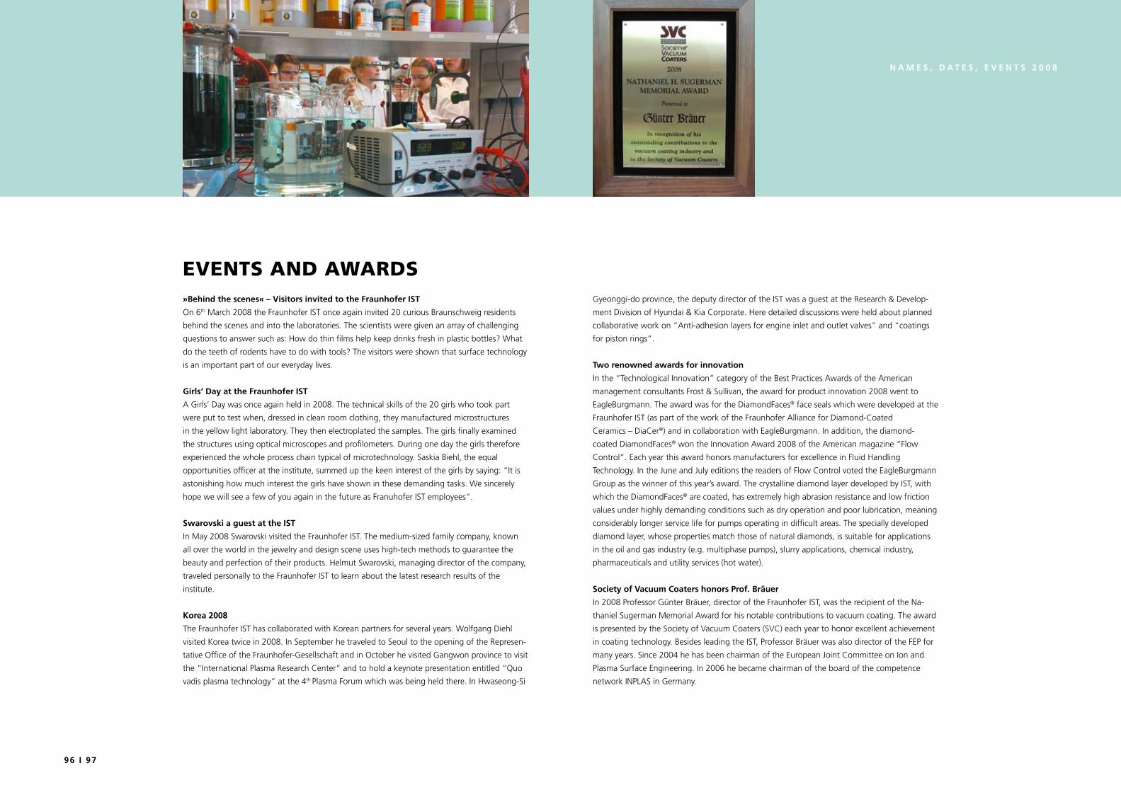
96 I 97
n a m e S , D a T e S , e v e n T S 2 0 0 8
events And AwARds»behind the scenes« – visitors invited to the Fraunhofer IST
On 6th March 2008 the Fraunhofer IST once again invited 20 curious Braunschweig residents
behind the scenes and into the laboratories. The scientists were given an array of challenging
questions to answer such as: How do thin films help keep drinks fresh in plastic bottles? What
do the teeth of rodents have to do with tools? The visitors were shown that surface technology
is an important part of our everyday lives.
Girls‘ Day at the Fraunhofer IST
A Girls’ Day was once again held in 2008. The technical skills of the 20 girls who took part
were put to test when, dressed in clean room clothing, they manufactured microstructures
in the yellow light laboratory. They then electroplated the samples. The girls finally examined
the structures using optical microscopes and profilometers. During one day the girls therefore
experienced the whole process chain typical of microtechnology. Saskia Biehl, the equal
opportunities officer at the institute, summed up the keen interest of the girls by saying: “It is
astonishing how much interest the girls have shown in these demanding tasks. We sincerely
hope we will see a few of you again in the future as Franuhofer IST employees”.
Swarovski a guest at the IST
In May 2008 Swarovski visited the Fraunhofer IST. The medium-sized family company, known
all over the world in the jewelry and design scene uses high-tech methods to guarantee the
beauty and perfection of their products. Helmut Swarovski, managing director of the company,
traveled personally to the Fraunhofer IST to learn about the latest research results of the
institute.
korea 2008
The Fraunhofer IST has collaborated with Korean partners for several years. Wolfgang Diehl
visited Korea twice in 2008. In September he traveled to Seoul to the opening of the Represen-
tative Office of the Fraunhofer-Gesellschaft and in October he visited Gangwon province to visit
the “International Plasma Research Center” and to hold a keynote presentation entitled “Quo
vadis plasma technology” at the 4th Plasma Forum which was being held there. In Hwaseong-Si
Gyeonggi-do province, the deputy director of the IST was a guest at the Research & Develop-
ment Division of Hyundai & Kia Corporate. Here detailed discussions were held about planned
collaborative work on “Anti-adhesion layers for engine inlet and outlet valves” and “coatings
for piston rings”.
Two renowned awards for innovation
In the “Technological Innovation” category of the Best Practices Awards of the American
management consultants Frost & Sullivan, the award for product innovation 2008 went to
EagleBurgmann. The award was for the DiamondFaces® face seals which were developed at the
Fraunhofer IST (as part of the work of the Fraunhofer Alliance for Diamond-Coated
Ceramics – DiaCer®) and in collaboration with EagleBurgmann. In addition, the diamond-
coated DiamondFaces® won the Innovation Award 2008 of the American magazine “Flow
Control”. Each year this award honors manufacturers for excellence in Fluid Handling
Technology. In the June and July editions the readers of Flow Control voted the EagleBurgmann
Group as the winner of this year’s award. The crystalline diamond layer developed by IST, with
which the DiamondFaces® are coated, has extremely high abrasion resistance and low friction
values under highly demanding conditions such as dry operation and poor lubrication, meaning
considerably longer service life for pumps operating in difficult areas. The specially developed
diamond layer, whose properties match those of natural diamonds, is suitable for applications
in the oil and gas industry (e.g. multiphase pumps), slurry applications, chemical industry,
pharmaceuticals and utility services (hot water).
Society of vacuum Coaters honors prof. bräuer
In 2008 Professor Günter Bräuer, director of the Fraunhofer IST, was the recipient of the Na-
thaniel Sugerman Memorial Award for his notable contributions to vacuum coating. The award
is presented by the Society of Vacuum Coaters (SVC) each year to honor excellent achievement
in coating technology. Besides leading the IST, Professor Bräuer was also director of the FEP for
many years. Since 2004 he has been chairman of the European Joint Committee on Ion and
Plasma Surface Engineering. In 2006 he became chairman of the board of the competence
network INPLAS in Germany.
98 I 99
p u b l I C a T I o n S
board memberships
Bandorf, R.: Forschungsvereinigung 3D-MID e. V., Mitglied.
Bewilogua, K.: Co-Chair Organizing Committee “1st Workshop
for International Standard of Diamond-like Carbon Coatings”,
Korea 2008.
Bewilogua, K.: International Conference on Metallurgical
Coatings and Thin Films (ICMCTF), Symposium Chairman
“Carbon and Nitride Materials”.
Bewilogua, K.: Programmkomitee “International Symposium
Friction, Wear and Wear Protection 2008”, Mitglied.
Bräuer, G.: Beirat der AMG – Coating Technologies, Mitglied.
Bräuer, G.: Aufsichtsrat der PEP Photonos European
Photovoltaics AG, Mitglied.
Bräuer, G.: International Council on Coatings on Glass (ICCG
e.V.), Mitglied des Vorstandes.
Bräuer, G.: Zentrum für Mikroproduktion e.V., Mitglied des
Vorstandes.
Bräuer, G.: Kompetenznetz “Industrielle Plasma-Oberflächen-
technik” (INPLAS e. V.), Vorstandsvorsitzender.
Bräuer, G.: Aufsichtsrat der PVA TePla AG, Mitglied.
Bräuer, G.: European Joint Committee on Plasma and Ion
Surface Engineering (EJC/PISE), Chairman.
Bräuer, G.: International Conference on Coatings on Glass
(ICCG), Mitglied des Organisationskomitees.
Bräuer, G.: Nano- und Materialinnovationen Niedersachsen e.
V. (NMN), Mitglied des Vorstands.
Bräuer, G.: Zeitschrift “Vakuum in Forschung und Praxis”,
Mitglied des Kuratoriums.
Bräuer, G.: Zentrum für Mikroproduktion e. V. (ZemPro).
Brand, C.: Arbeitskreis Plasmaoberflächentechnologie (AK
Plasma), Mitglied des Koordinierungsausschusses.
Brand, C.: Europäische Forschungsgesellschaft Dünne Schich-
ten e. V. (EFDS), Mitglied.
Brand, J.: Europäische Forschungsgesellschaft Dünne Schich-
ten e. V. (EFDS), Leitung des Fachausschusses “Tribologische
Schichten”.
Brand, J.: Gesellschaft für Tribologie (GfT), Mitglied.
Brand, J.: International Colloquium Tribology, Tribology and
Lubrication Engineering, Mitglied im Programme Planning
Committee.
Diehl, W.: Arbeitskreis Plasmaoberflächentechnologie (AK
Plasma), Mitglied.
Diehl, W.: Europäische Forschungsgesellschaft Dünne Schich-
ten e. V. (EFDS), Mitglied des Vorstands.
Diehl, W.: ForschungRegion Braunschweig, Mitglied des
Lenkungskreises.
Diehl, W.: Society of Vacuum Coaters (SVC), Mitglied des
“International Relations Committee”.
Diehl, W.: Society of Vacuum Coaters (SVC), Mitglied des
Ausschusses “Tribological and Decorative Coatings”.
Diehl, W.: Technologietransferkreis ForschungRegion
Braunschweig, Mitglied.
Diehl, W.: Glass Performance Days, Finnland, Mitglied des
“Advisory Committee”.
Dietz, A.: Arbeitsgemeinschaft Elektrochemischer Forschung
(AGEF), Mitglied.
Dietz, A.: Deutsche Gesellschaft für Galvano- und Oberflä-
chentechnik e. V. (DGO), Mitglied des Vorstands.
Dietz, A.: Deutsche Gesellschaft für Galvano- und Ober-
flächentechnik e. V. (DGO), stellvertretender Vorsitzender
Ortsgruppe Niedersachsen.
Dietz, A.: Fachausschuss Forschung der DGO, Mitglied.
Dietz, A.: Gesellschaft für Korrosionsschutz (GfKorr), Mitglied.
Gäbler, J.: European Technology Platform for Advanced
Materials and Technologies EuMaT, Mitglied.
Gäbler, J: Industrie-Arbeitskreis “Werkzeugbeschichtungen
und Schneidstoffe”, Leitung.
Gäbler, J.: Kompetenznetz Industrielle Plasma-Oberflächen-
technik INPLAS, Arbeitsgruppenleiter Werkzeuge.
Gäbler, J.: VDI-Richtlinien-Fachausschuss “CVD-Diamant-
Werkzeuge”, Mitglied.
Jung, T.: Arbeitskreis “Mechanische und Schutzschichtan-
wendungen” im Kompetenzzentrum Ultradünne funktionale
Schichten Dresden-Chemnitz, Mitglied.
Klages, C.-P.: Fachausschuss “Oberflächen und Beschichtun-
gen in der Bio- und Medizintechnik” (FABM) der Europäischen
Forschungsgesellschaft Dünne Schichten e. V. (EFDS), Mitglied.
100 I 101
p u b l I C a T I o n S
Schäfer, L.: Nano- und Materialinnovationen Niedersachsen
e. V. (NMN), Mitglied.
Schäfer, L.: Nanotechnologie-Kompetenzzentrum Ultrapräzise
Oberflächenbearbeitung CC UPOB e. V., Mitglied.
Schäfer, L.: VDI-Richtlinien-Fachausschuss “CVD-Diamant-
Werkzeuge”, Mitglied.
Schiffmann, K.: Arbeitskreis “Rasterkraftmikroskopie in der
Werkstoffwissenschaft” im Fachausschuss “Metallographie”
der DGM, Mitglied im Lenkungsausschuss.
Thomas, M.: Fachausschuss “Oberflächen und Beschichtungen
in der Bio- und Medizintechnik” (FABM) der Europäischen
Forschungsgesellschaft Dünne Schichten e. V. (EFDS), Mitglied.
Vergöhl, M.: Kompetenznetz Optische Technolgien - Photonic-
Net GmbH, Mitglied.
Weber, M.: Europäische Forschungsgesellschaft Dünne Schich-
ten e. V. (EFDS), Leitung des Fachausschusses “Beschichtung
von Formen und Werkzeugen für die Kunststoffverarbeitung”.
Klages, C.-P.: International Journal of Refractory Metals & Hard
Materials, Mitglied des Editorial Advisory Boards.
Klages, C.-P.: Projektbegleitende Arbeitsgruppe “Sensorik” der
Fachhochschule Westküste, Mitglied.
Klumpp, G.: Arbeitskreis “Ausbildung” der Fraunhofer-
Gesellschaft, Mitglied.
Klumpp, G.: Lenkungsgruppe “Aus- und Weiterbildung” des
Zentralverbands Oberflächentechnik, Mitglied.
Neumann, F.: DIN-Normenausschuss Photokatalyse NA 062-
02-93 AA, Mitglied und Vorsitz des Arbeitskreises
“Photokatalytischer Lumineszenzabbau”, DIN Deutsches
Institut für Normung e. V..
Schäfer, L.: Industriearbeitskreis “Werkzeugbeschichtungen
und Schneidstoffe”, Mitglied.
Schäfer, L.: International Conference on New Diamond and
Nanocarbons NDNC-2008, Program Committee Member.
International Guests
Mr. Owen Sheedy, Institute of Technology, Department of
Mechanical Engineering, Tallaght, Ireland, September 2007 –
August 2008.
patent applications
Bandorf, R.; Vergöhl, M.; Mark, G.: Magnetron Plasma System.
Bandorf, R.; Jung, T.; Ortner, K.: Vorrichtung und Verfahren
zum Hochleistungs-Puls-Gasfluss-Sputtern.
Eichler, M.; Meyer M.: Verfahren zur wiederholten Bestim-
mung der Bondfestigkeit aneinander gebondeter Substrate.
Klages, C.-P.; Thomas, M.: Strukturierte Plasmabehandlung
von Oberflächen mit gasdurchströmten porösen Elektroden.
Thomas, M.; Klages, C.-P.; Zänker, A.: Vorrichtung und Verfah-
ren zur mikrostrukturierten Plasmabehandlung.
Wallendorf, T.; Bandorf, R.; Vergöhl, M.: Anordnung und
Verfahren zur Erzeugung eines Plasmas mit definiertem und
stabilen Ionisationszustand.
102 I 103
p u b l I C a T I o n S
publications IST 2008
Bandorf, R.; Lüthje, H.; Sick, J.-H.; Biehl, S.; Diehl, W.:
Multifunctional parts by functionalisation solutions: How to
integrate intelligence in rapid parts. In: Meyer, Rudolf (Ed.):
Fraunhofer-Allianz Rapid Prototyping: High-Tech Solutions and
Concepts – Hochtechnologielösungen und anwendbare Praxis-
Konzepte: Euro-uRapid 2008: Proceedings of the International
User‘s Conference on Rapid Prototyping & Rapid Tooling &
Rapid Manufacturing, Berlin, Germany, September 23–24,
2008. Magdeburg: Fraunhofer-Allianz Rapid Prototyping,
2008, p. 85–96.
Bandorf, R.; Falkenau, S.; Schiffmann, K.; Gerdes, H.;
Heckmann, U.: Properties of Nichrome sputtered by HIPIMS in
unipolar and DC-superimposed mode. In: Society of Vacuum
Coaters (SVC): Society of Vacuum Coaters: 51st Annual Tech-
nical Conference Proceedings, Chicago, IL, USA, April 19–24,
2008. Albuquerque: SVC, 2008, p. 317–320.
Bandorf, R.; Diehl, W.; Heckmann, U.; Holeczek, H.; Klotzbach,
U.; Kondruweit-Reinema, S.; Leson, A.; Metzner, M.; Pflug, A.;
Zimmer, O.: Thesen und Trends – mit funktionalen Oberflächen
in die Zukunft. In: Vakuum in Forschung und Praxis 20 (2008),
5, S. 14–20.
Bandorf, R.; Paulkowski, D.; Schiffmann, K. I.; Küster, R.:
Tribological improvement of moving microparts by application
of thin films and micropatterning. In: Journal of physics:
Condensed matter 20 (2008), 35, 354018.
Bedenbecker, M.; Bandorf, R.; Bräuer, G.; Lüthje, H.; Gatzen,
H. H.: Hard and soft magnetic materials for electromagnetic
microactuators. In: Microsystem technologies 14 (2008),
12, p. 1949–1954.
Behrens, B.-A.; Bach, F.-W.; Bräuer, G.; Möhwald, K.; Deißler,
T. A.; Paschke, H.; Weber, M.; Bistron, M.: Steigerung des
Verschleißwiderstandes von Schmiedewerkzeugen: Verschleiß-
reduzierung an Präzisionsschmiedegesenken durch borhaltige
PACVD-Beschichtungen. In: wt Werkstattstechnik online 98
(2008), 10, S. 805–812.
Biehl, S.: Intelligente Unterlegscheiben. In: Swiss engineering
(2008), 10, S. 47.
Biehl, S.: Intelligente Unterlegscheiben messen die Spannkraft
in Schraubverbindungen. In: Sensormagazin (2008), 2,
S. 28–29.
Biehl, S.; Woitschach, O.; Staufenbiel, S.; Brill, C.: Piezo
resistive thin film sensor system. In: IEEE Sensors, Lecce, Italy,
October 26–29, 2008. Piscataway, NJ: IEEE, 2008,
p. 1572–1575.
Biehl, S.; Woitschach, O.; Staufenbiel, S.; Schuller, B.; Wittmer,
R.: Piezo resistive thin-film sensor as safety system in high
speed cutting processes. In: VDI/VDE-Gesellschaft Mess- und
Automatisierungstechnik: Eurosensors XXII: Proceedings,
Dresden, Germany, September 7–10, 2008. Düsseldorf: VDI/
VDE-Ges. Mess- und Automatisierungstechnik, 2008,
p. 173–175.
Biehl, S.; Goericke, F.; Wolf, L.; Staufenbiel, S.; Delan, A.;
Schultheiß, E.: Suitability of sputtered titanium dioxide layers
for low-temperature measurement of oxygen concentration.
In: VDI/VDE-Gesellschaft Mess- und Automatisierungstechnik:
Eurosensors XXII: Proceedings, Dresden, Germany, September
7–10, 2008. Düsseldorf: VDI/VDE-Ges. Mess- und Automati-
sierungstechnik, 2008, p. 1590–1593.
Borris, J.; Thomas, M.; Zänker, A.; Klages, C.-P.; Möbius,
A.; Elbick, D.; Weidlich, E.-R.; Feldmann, K.; Schüßler, F.:
Plasma-printing and galvanic metallization hand in hand – a
new technology for the cost-efficient manufacture of flexible
printed circuits. In: Dzur, Birger (Hrsg.): XV. Workshop Plasma-
und Oberflächentechnik: Tagungsband, 26. und 27. Juni 2008.
Ilmenau, 2008, S. 43–48.
Brand, J.: DLC – ein Schmierstoff mit Zukunft: Diamant-
ähnlicher Kohlenstoff. In: JOT + Oberfläche: Journal für
Oberflächentechnik (2008), 6, S. 42–45.
Bräuer, G.; Bandorf, R.; Biehl, S.; Dietz, A.; Lüthje, H.; Vergöhl,
M.: Smart coatings for intelligent surfaces. In: Vacuum‘s Best
20 (2008), S1, p. 34–37.
Bräuer, G.: Magnetronzerstäubung – Meilensteine aus 20
Jahren. In: Vakuum in Forschung und Praxis 20 (2008), 2,
S. 30–32.
Cabral, G.; Gäbler, J.; Lindner, J.; Grácia, J.; Polini, R.: A study
of diamond film deposition on WC-Co inserts for graphite ma-
chining: Effectiveness of SiC interlayers prepared by HFCVD.
In: Diamond and related materials 17 (2008), 6,
p. 1008–1014.
Corbella, C.; Bialuch, I.; Kleinschmidt, M.; Bewilogua, K.:
Modified DLC coatings prepared in a large-scale reactor by
dual microwave/pulsed-DC plasma-activated chemical vapour
deposition. In: Thin solid films 517 (2008), 3, p. 1125–1130.
Diehl, W.; Bandorf, R.; Heckmann, U.; Holeczek, H.; Klotzbach,
U.; Kondruweit-Reinema, S.; Leson, A.; Metzner, M.; Pflug,
A.; Zimmer, O.: Forschungsbedarf zur Erzeugung funktionaler
Oberflächen. In: Ruprecht, Robert (Hrsg.): Forschungszentrum
Karlsruhe: Karlsruher Arbeitsgespräche Produktionsforschung
2008: Spitzentechnologien für den Wirtschaftsmotor Produkti-
on: Ergebnisse aus dem BMBF-Rahmenkonzept “Forschung für
die Produktion von morgen”, Tagungsband zur Veranstaltung
am 11. und 12. März 2008, Kongresszentrum, Stadthalle
Karlsruhe. Karlsruhe: Forschungszentrum Karlsruhe, 2008,
S. 386–393. (Wissenschaftliche Berichte/FZKA-PFT 214).
Diehl, W.; Heckmann, U.; Holeczek, H.; Klotzbach, U.;
Kondruweit-Reinema, S.; Leson, A.; Metzner, M.; Pflug, A.;
Zimmer, O.; Bandorf, R. (Projektleiter); Fraunhofer-Institut für
Schicht- und Oberflächentechnik (IST); Fraunhofer-Institut für
Werkstoff- und Strahltechnik (IWS); Fraunhofer-Institut für
Produktionstechnik und Automatisierung (IPA): Produktions-
technik zur Erzeugung funktionaler Oberflächen: Status und
Perspektiven. Braunschweig, 2008.
Diehl, W.: Glänzende Aussichten am Fraunhofer-Institut für
Schicht- und Oberflächentechnik. In: nanotechnologie aktuell
(2008), 1, S. 128–131.
Eichler, M.; Berger, C.; Thomas, M.; Klages, C.-P.: Allseitige
Innenbeschichtung von fluidischen Systemen. In: Institut für
Bioprozess- und Analysenmesstechnik: Technische Systeme für
die Lebenswissenschaften: 14. Heiligenstädter Kolloquium,
Heilbad Heiligenstadt, 22. bis 24. September 2008. Heiligen-
stadt: Inst. für Bioprozess- und Analysenmesstechnik, 2008,
S. 159–166.
104 I 105
p u b l I C a T I o n S
Eichler, M.; Michel, B.; Thomas, M.; Gabriel, M.; Klages, C.-P.:
Atmospheric-pressure plasma pretreatment for direct bonding
of silicon wafers at low temperatures. In: Surface and Coatings
Technology 203 (2008), 5–7, p. 826–829.
Eichler, M.; Michel, B.; Thomas, M.; Klages, C.-P.: Kinetics of
silanol condensation for low-temperature direct bonding. In:
Semiconductor Wafer Bonding 10: Science, Technology, and
Applications, Tenth International Symposium on Semiconduc-
tor Wafer Bonding, Honolulu, Hawaii, October 14–16, 2008.
Pennington, NJ: Electrochemical Soc., 2008, p. 369–376. (ECS
transactions 16, 8).
Gäbler, J.: Feinst- und Mikroschleifen mit CVD-Diamantschleif-
werkzeugen. In: Diamond business (2008), 4, S. 6–10.
Gäbler, J.: High-Tech-Haut für Schwerstarbeiter. In: Werkzeug
& Formenbau 17 (2008), 1, S. 72–75.
Gäbler, J.; Schäfer, L.; Pleger, S.: Precision grinding with CVD
diamond coated grinding tools. In: Brussel, H. Van (Ed.)
u. a.: European Society for Precision Engineering and Nano-
technology: Proceedings of the 10th anniversary international
conference of the European society for precision engineering
and nanotechnology, Volume 1, Zurich, Switzerland, May
18–22, 2008. Bedford: euspen, 2008, p. 78–82.
Gerdes, H.; Schmidt, M.; Wellhausen, J.; Bandorf, R.;
Bräuer, G.: Investigations on high power impulse magnetron
sputtering by optical emission spectroscopy of NiCr in different
compositions (40/60 and 80/20). In: De Gryse, R. (Ed.) u. a.:
Proceedings of ICTF14 & RSD2008. Ghent, Belgium, 2008,
p. 92–95.
Heckmann, U.; Bandorf, R.; Diehl, W.; Holeczek, H.; Klotzbach,
U.; Kondruweit-Reinema, S.; Leson, A.; Metzner, M.; Pflug, A.;
Zimmer, O.: Produktionstechnik für funktionale Oberflächen:
Perspektiven, Forschungs- und Handlungsbedarf.
In: wt Werkstattstechnik online 98 (2008), 6, S. 481–485.
Hinze, A.; Klages, C.-P.; Zänker, A.; Thomas, M.; Wirth, T.;
Unger, W. E. S.: ToF-SIMS imaging of DBD-plasma-printed
microspots on BOPP substrates. In: Plasma processes and
polymers 5 (2008), 5, p. 460–470.
Hoffmeister, H.-W.; Schuller, B. C.; Wittmer, R.; Biehl, S.;
Woitschach, O.; Staufenbiel, S.: Sensoren detektieren kritische
Wuchtzustände. In: Die Holzbearbeitung HOB 2008, 10,
S. 81–83.
Klages, C.-P.; Grishin, A.; Hinze, A.; Thomas, M.; Borris,
J.: Investigations of plasma-amination of polymer surfaces
by dielectric barrier discharges. In: IOM Communications
Limited <London> u. a.: EURADH 2008/Adhesion ´08: 10th
International Conference on the Science and Technology of
Adhesion and Adhesives, St. Catherine‘s College, Oxford, UK,
September 3–5, 2008. London: IOM Communications Ltd.,
2008, p. 135–138.
Klages, C.-P.; Grishin, A.: Plasma amination of low-density
polyethylene by DBD afterglows at atmospheric pressure. In:
Plasma processes and polymers 5 (2008), 4, p. 368–376.
Klages, C.-P.; Grishin, A.: Quantitative ATR FT-IR analysis of
chemically derivatized plasma-modified polymer surfaces. In:
Plasma processes and polymers 5 (2008), 4, p. 359–367.
Kölker, W.; van den Berg, H.; Hünsche, I.; Kursawe, S.;
Kessel, H. U.; Richter, V.; Keunecke, M.: Cutting tools made
from nanoscale materials with superhard coatings for dry
machining and applications in hardened steels and cast iron.
In: Bundesministerium für Bildung und Forschung (BMBF):
Production Research for Micro- and Nano Technology, MiNaT,
Stuttgart, October 7–9, 2008. Eggenstein-Leopoldshafen,
2008, p. 86–89.
Kubart, T.; Nyberg, T.; Pflug, A.; Kohl, D.; Wuttig, M.; Berg, S.:
Sputtering yield amplification for targets operated in reactive
mode. In: De Gryse, R. (Ed.) u. a.: Proceedings of ICTF14 &
RSD2008. Ghent, Belgium, 2008, p. 41–44.
Lucas, N.; Hinze, A.; Klages, C.-P.; Büttgenbach, S.: Design
and optimization of dielectric barrier discharge microplasma
stamps. In: Journal of physics D 41 (2008), 19, 194012 (5pp).
Münz, W. D.; Schenkel, M.; Kunkel, S.; Paulitsch, M.;
Bewilogua, K.: Industrial applications of HIPIMS. In: Journal of
physics, conference series 100 (2008), getr. Zählung.
Neubert, T.; Graumann, T.; Neumann, F.; Vergöhl, M.: Photo-
katalytische Titandioxidbeschichtung aus der Gasphase. In:
JOT + Oberfläche: Journal für Oberflächentechnik 48 (2008),
9, S. 48–50.
Neubert, T.; Werner, O.; Neumann, F.; Vergöhl, M.: Preparation
of photocatalytically active TiO2 layers on polycarbonate by
reactive magnetron sputtering. In: Society of Vacuum Coaters
(SVC): Society of Vacuum Coaters: 51st Annual Technical
Conference Proceedings, Chicago, IL, USA, April 19–24, 2008.
Albuquerque: SVC, 2008, p. 143–147.
Paulkowski, D.; Bandorf, R.; Achilles, S.; Pape, F.; Gatzen, H.
H.; Bräuer, G.: Studies on diamond-like carbon coatings for
the application in micro actuators. In: Advanced engineering
materials 10 (2008), 7, p. 644–647.
Paulkowski, D.; Bandorf, R.; Schiffmann, K.: Tribology of
carbon based coatings on patterned surfaces in flat-flat micro
contact. In: Gesellschaft für Tribologie <Aachen>: Reibung,
Schmierung und Verschleiß: Forschung und praktische
Anwendung, Band I: 49; Tribologie-Fachtagung, 22. bis 24.
September 2008 in Göttingen: Werkstoffe und Werkstoff-
technologien, Dünne Schichten und Oberflächentechnologien,
Schmierstoffe und Schmierungstechnik. Aachen: Gesellschaft
für Tribologie, 2008, 06/1–06/8.
Petrik, M.; Wittorf, R.; Thomsen, H.; Kaestner, P.; Kropp, J. P.:
Beschichtungen für Zahnräder. In: Vakuum in Forschung und
Praxis 20 (2008), 4, S. 6–12.
Pflug, A.; Siemers, M.; Szyszka, B.; Geisler, M.; Beckmann,
R.: Gas flow and plasma simulation for parallel plate PACVD
reactors. In: Society of Vacuum Coaters (SVC): Society of Va-
cuum Coaters: 51st Annual Technical Conference Proceedings,
Chicago, IL, USA, April 19–24, 2008. Albuquerque: SVC,
2008, p. 3–7.
Polenzky, C.; Rickers, C.; Vergöhl, M.: Cosputtered SiO2 and
Ta2O5R – influence of temperature and composition to the
optical functionality of a Rugate filter. In: Spee, C.I.M.A. (Ed.)
u.a.: 7th International Conference on Coatings on Glass and
Plastics ICCG7: Advanced Coatings for Large-Area or High-
Volume Products, Eindhoven/Veldhoven, The Netherlands,
June 15–19, 2008. Eindhoven: TNO Science and Industry,
2008, p. 271–272.
Ruske, F.; Pflug, A.; Sittinger, V.; Werner, W.; Szyszka, B.; Chris-
tie, D. J.: Reactive deposition of aluminium-doped zinc oxide
thin films using high power pulsed magnetron sputtering. In:
Thin solid films 516 (2008), 14, p. 4472–4477.
Schiffmann, K. I.: Microtribological/mechanical testing in 0, 1
and 2 dimensions: A comparative study on different materials.
In: Wear 265 (2008), 11–12, p. 1826–1836.
106 I 107
p u b l I C a T I o n S
Siemers, M.; Pflug, A.; Szyszka, B.: Particle-in-cell Monte Carlo
analysis of anomalous target erosion in magnetron sputtering.
In: Society of Vacuum Coaters (SVC): Society of Vacuum Coa-
ters: 51st Annual Technical Conference Proceedings, Chicago,
IL, USA, April 19–24, 2008. Albuquerque: SVC, 2008, p.
43–48.
Sittinger, V.; Ruske, F.; Werner, W.; Jacobs, C.; Szyszka, B.;
Christie, D. J.: High power pulsed magnetron sputtering of
transparent conducting oxides. In: Thin solid films 516 (2008),
17, p. 5847–5859.
Sittinger, V.; Szyszka, B.; Bandorf, R.; Vergöhl, M.; Pflug, A.;
Christie, D. J.; Ruske, F.: Research on promising applications
for high power pulse magnetron sputtering. In: Society of
Vacuum Coaters (SVC): Society of Vacuum Coaters: 51st
Annual Technical Conference Proceedings, Chicago, IL, USA,
April 19–24, 2008. Albuquerque: SVC, 2008, p. 293–301.
Szyszka, B.; Gombert, A.; May, C.; Elsaesser, C.: Development
of advanced transparent conductive electrodes for large-area
opto-electronic devices. In: Spee, C.I.M.A. (Ed.) u. a.: 7th
International Conference on Coatings on Glass and Plastics
ICCG 7: Advanced Coatings for Large-Area or High-Volume
Products, Eindhoven/Veldhoven, The Netherlands, June
15–19, 2008. Eindhoven: TNO Science and Industry, 2008, p.
237–238.
Szyszka, B.; Gombert, A.; Loebmann, P.; May, C.; Elsaesser, C.:
Development of advanced transparent conductive electrodes
for large-area opto-electronic devices. In: Society of Vacuum
Coaters (SVC): Society of Vacuum Coaters: 51st Annual Tech-
nical Conference Proceedings, Chicago, IL, USA, April 19–24,
2008. Albuquerque: SVC, 2008, p. 395–401.
Ulrich, S.; Pflug, A.; Szyszka, B.: Optical and XRR methods for
analysis and design of low-e coatings and PDP EMI filters. In:
Society of Vacuum Coaters (SVC): Society of Vacuum Coaters:
51st Annual Technical Conference Proceedings, Chicago, IL,
USA, April 19–24, 2008. Albuquerque: SVC, 2008,
p. 386–390.
Ulrich, S.; Pflug, A.; Schiffmann, K. I.; Szyszka, B.: Optical
modeling and XRR/AFM characterization of highly conductive
thin Ag layers. In: Physica status solidi C 5 (2008), 5,
p. 1235–1239.
Vergöhl, M.; Werner, O.; Bruns, S.: Properties of ZrO2 thin
films deposited by plasma assisted pulsed reactive magnetron
sputtering. In: Society of Vacuum Coaters (SVC): Society of Va-
cuum Coaters: 51st Annual Technical Conference Proceedings,
Chicago, IL, USA, April 19–24, 2008. Albuquerque: SVC,
2008, p. 492–497.
Vergöhl, M.; Werner, O.; Bruns, S.; Wallendorf, T.; Mark, G.:
Superimposed MF-HiPIMS processes for the deposition of ZrO2
thin films. In: Society of Vacuum Coaters (SVC): Society of Va-
cuum Coaters: 51st Annual Technical Conference Proceedings;
Chicago, IL, USA, April 19–24, 2008. Albuquerque: SVC,
2008, p. 307–312.
Wallendorf, T.; Vergöhl, M.; Werner, O.; Bandorf, R.: HIPIMS/
HiPIMS process design with multi channel pulse pattern
controller. In: Society of Vacuum Coaters (SVC): Society of
Vacuum Coaters: 51st Annual Technical Conference Procee-
dings, Chicago, IL, USA, April 19–24, 2008. Albuquerque:
SVC, 2008, p. 161–165.
Weber, M.; Brand, J.; Kaestner, P.; Paschke, H.; Thomsen, H.:
Neue Schutzschichten für Werkzeuge der Warmformgebung.
In: Gesellschaft für Fertigungstechnik <Stuttgart>: Schriftliche
Fassung der Vorträge zum Fertigungstechnischen Kolloquium
am 10. und 11. September in Stuttgart, FtK 2008, Ferti-
gungstechnisches Kolloquium Stuttgart. Stuttgart: Ges. für
Fertigungstechnik, 2008, S. 319–332.
108 I 109
p u b l I C a T I o n S
lectures, posters
Bandorf, R.; Gerdes, H.; Vergöhl, M.; Sittinger, V.; Szyszka, B.;
Wallendorf, T.; Mark, G.: Investigation of HiPIMS in unipolar,
bipolar and superimposed mode, 35th International Confe-
rence on Metallurgical Coatings and Thin Films ICMCTF 2008,
San Diego, CA, USA, April/Mai 2008.
Bandorf, R.; Gerdes, H.; Schmidt, M.: Influence of pulse
packages on the peak power and ionisation of target material
of HiPIMS processes, Fifth HIPIMS days Conference, Venlo,
The Netherlands, July 2008.
Bandorf, R.; Gerdes, H.; Bräuer, G.: Influence of the Cathode
Impedance and Target Material on the Resulting Peak Power
at High Power Impulse Magnetron Sputtering HiPIMS, 11th
International Conference on Plasma Surface Engineering PSE
2008, Garmisch-Partenkirchen, September 2008.
Bandorf, R.; Schmidt, M.; Gerdes, H.; Hesse, F.; Bräuer, G.: In-
vestigation of Ti3SiC2-Films prepared with DC, HiPIMS and DC
superimposed HiPIMS, 11th International Conference on Plas-
ma Surface Engineering PSE 2008, Garmisch-Partenkirchen,
September 2008.
Bandorf, R.: Direkt applizierte Dünnschicht-DMS für intelligen-
te Produkte, Industrie Workshop “Sputter-Dehnungsmess-
streifen”, Braunschweig, November 2008.
Bandorf, R.: Einführung: Was ist HiPIMS?, INPLAS e. V. HiPIMS-
Workshop, Braunschweig, November 2008.
Bandorf, R.: Produktionstechnik zur Erzeugung funktionaler
Oberflächen – Thesen und Trends, PhotonicNet Partner
Workshop, Hameln, November 2008.
Bethke, R.: Trends in Patents on Plasama and Surface Enginee-
ring, 11th International Conference on Plasma Surface Engi-
neering PSE 2008, Garmisch-Partenkirchen, September 2008.
Bewilogua, K.; Keunecke, M.; Weber, M.; Thomsen, H.; Wei-
gel, K.; Wittorf, R.: Advanced tribological coatings – prepared
in industrial scale machines, 35th International Conference on
Metallurgical Coatings and Thin Films ICMCTF 2008,
San Diego, CA, USA, April/May 2008.
Bewilogua, K.; Keunecke, M.; Wittorf, R.; Münz, W.-D.; Schen-
kel, M.; Kunkel, S.: Magnetron sputter deposition of hard
and superhard a-C:H coatings, Fifth HIPIMS days Conference,
Venlo, The Netherlands, July 2008.
Bewilogua, K.; Bialuch, I.; Ruske, H.; Weigel, K.; Grün, R.;
Okun, J.; Seher, I.; Günther, H.-J.: Carbon based multilayer
coatings prepared by PACVD with industrial scale up, 11th
International Conference on Plasma Surface Engineering PSE
2008, Garmisch-Partenkirchen, September 2008.
Bialuch, I.; Bewilogua, K.; Ruske, H.; Weigel, K.: Multilagen-
Konzepte zur tribologischen Optimierung von Antihaftschich-
ten, EFDS-Workshop „Kohlenstoffschichten – Tribologische
Eigenschaften und Verfahren zu ihrer Herstellung”, Dortmund,
June 2008.
Bialuch, I.; Ortner, K.; Bewilogua, K.; Augustin, W.; Albert, F.;
Geddert, T.; Scholl, S.: Modified DLC coatings with anti-fouling
properties (Poster), 11th International Conference on Plasma
Surface Engineering PSE 2008, Garmisch-Partenkirchen,
September 2008.
Biehl, S.: Suitability of sputtered titanium dioxid layers for low
temperature measurement of oxygen concentration (Talk),
Eurosensors Conference 2008, Dresden, September 2008.
Biehl, S.; Woitschach, O.; Staufenbiel, S.; Schuller, B.; Ronald
Wittmer, R.: Piezo resistive thin film sensor as safety system in
high speed cutting processes (Poster), Eurosensors Conference
2008, Dresden, September 2008.
Biehl, S.: Piezo resistive Thin Film Sensor System (Talk), IEEE
Sensor Conference 2008, Lecce, Italy, October 2008.
Borris, J.; Zänker, A.; Thomas, M.; Klages, C.-P.: Plasma
Printing – a new process for the manufacture of RFID antennas
(Talk), 5th Central and Eastern European Conference on
Packaging, Prague, Czech Republic, April 2008.
Borris, J.; Thomas, M.; Zänker, A.; Klages, C.-P.; Möbius, A.;
Elbick, D.; Weidlich, E.-R.; Feldmann, K.; Schüßler, F.: Plasma-
printing and galvanic metallization hand in hand – a new tech-
nology for the cost-efficient manufacture of flexible printed
circuits (Talk), XV. Workshop Plasma- und Oberflächentechnik,
Ilmenau, June 2008.
Borris, J.; Dohse, A.; Hinze, A.; Thomas, M.; Klages, C.-P.;
Möbius, A.; Elbick, D.; Weidlich, E.-R.: Improvement of the
adhesion of a galvanic metallization of polymers by surface
functionalization using dielectric barrier discharges at atmos-
pheric pressure (Poster), 11th International Conference on Plas-
ma Surface Engineering PSE 2008, Garmisch-Partenkirchen,
September 2008.
Brand, J.: Effiziente Anlagenkonzepte: Von der Anlieferung bis
zum Versand (Talk), Fraunhofer Technologiezirkel “Potenziale
der Oberflächentechnik”, Braunschweig, April 2008.
Brand, J.: Tribologie – Reduzierung von Reibung und
Verschleiß (Talk), Fraunhofer Technologiezirkel “Potenziale der
Oberflächentechnik”, Braunschweig, April 2008.
Brand, J.: Oberflächentechnologien – Reduzierung von
Reibung und Verschleiß (Talk), Fraunhofer Technologiezirkel
“Neue Werkstoffe und Technologien”, Darmstadt, Germany,
September 2008.
110 I 111
p u b l I C a T I o n S
Bräuer, G.: Optische Funktionsschichten für innovative
Produkte, Fraunhofer Technologiezirkel “Potenziale der
Oberflächentechnik”, Braunschweig, April 2008.
Bräuer, G.: Surface technology for Vehicle Construction, Fifth
HIPIMS days Conference, Venlo, The Netherlands, July 2008.
Bräuer, G.: Hard coatings produced by plasma process – Deve-
lopments at Fraunhofer IST, 3ème Congrès “INTERSURFACES”,
Saint Etienne, France, October 2008
Corbella, C.; Bialuch, I.; Kleinschmidt, M.; Bewilogua, K.:
Modified DLC coatings prepared in a large-scale reactor by
dual microwave/pulsed-DC plasma-activated chemical vapour
deposition, 35th International Conference on Metallurgical
Coatings and Thin Films ICMCTF 2008, San Diego, CA, USA,
April/May 2008.
Corbella, C.; Bialuch, I.; Kleinschmidt, M.; Bewilogua, K.:
Up-scaling the production of modified DLC coatings in the
framework of plasma polymerization processes, European Ma-
terials Research Society Spring Meeting EMRS ´08, Strasbourg,
France, May 2008.
Dewald, W.; Sittinger, V.; Werner, W.; Jacobs, C.; Szyszka, B.:
Optimization of process parameters for sputtering of ceramic
ZnO:Al2O3 targets for a-Si:H/mc-Si:H solar cells (Poster), 2nd
International Symposium on Transparent Conductive Oxides,
Crete, Greece, October 2008.
Diehl, W.: Forschungsbedarf zur Erzeugung funktionaler
Oberflächen, 9. Karlsruher Arbeitsgespräche, Karlsruhe, March
2008.
Diehl, W.: Hard coatings produced by plasma processes –
technology and recent applications, 7th Iberian Vacuum
Meeting (RIVA7), Lisbon, Portugal, June 2008.
Diehl, W.: Thin coatings for automotive technology, Fraun-
hofer Automotive Symposium, Hyundai-Kia R&D Center,
Hwasung-Si, Korea, September 2008.
Diehl, W.: Hard coatings produced by plasma processes –
technology and recent applications, Fraunhofer Automotive
Symposium, Hyundai-Kia R&D Center, Hwasung-Si, Korea,
September 2008.
Diehl, W.: Transparent scratch protection coatings with
nanocomposites, SAMSUNG ELECTRONICS, Suwon, Korea,
September 2008.
Diehl, W.: Production Technology for the Generation of Func-
tional Surface, 8th Symposium of European Vacuum Coaters,
Anzio, Italy, September 2008.
Diehl, W.: Thin coatings for automotive technology, AutoIn-
dustry.AutoComponents, Togliatti, Russia, October 2008.
Diehl, W.: Thin film solar cell technology in Germany, NanoS-
Mat2008, Barcelona, Spain, October 2008.
Diehl, W.: Future Trend Plasma – Functional Coatings made
at Fraunhofer IST, Plasma Forum, Gangwon Province, Korea,
November 2008.
Dietz, A.: Neue Verfahren zur Metallisierung von Kunststoffen,
9. Leipziger Kunststofftag, Leipzig, May 2008.
Dietz, A.; Klumpp, G.: New process for the Magnesium Metal-
lization, 17th Interfinish Congress, Busan, Korea, June 2008.
Dietz, A.: Neue Entwicklungen in der galvanischen Disper-
sionsabscheidung, 11. Werkstofftechnisches Kolloquium,
Chemnitz, October 2008.
Eichler, M.; Thomas, M.; Klages, C.-P.: Neue Erkenntnisse zum
Einsatz von Barrierenentladungen beim Vorbehandeln diverser
Werkstoffe: Vorbehandeln zur Verbesserung der Haftung beim
Kleben, Lackieren, Bedrucken, Beschichten (Talk), Seminar
“Oberflächenvorbehandlung”, FH Hannover, February 2008.
Eichler, M.; Michel, B.; Thomas, M.; Gabriel, M.; Klages, C.-P.:
Atmospheric-pressure plasma pretreatment for direct bonding
of silicon wafers at low temperatures (Talk), International
Conference On Metallurgical Coatings And Thin Films ICMCTF
2008, San Diego, CA, USA, April/May 2008.
Eichler, M.; Berger, C.; Thomas, M.; Klages, C.-P.: Allseitige
Innenbeschichtung von fluidischen Systemen (Talk), 14.
Heiligenstädter Kolloquium, Heiligenstadt, September 2008.
Eichler, M.; Michel, B.; Thomas, M.; Klages, C.-P.: 10th
International Symposium on Semiconductor Wafer Bonding:
Science, Technology and Applications (Talk), Honolulu, HI,
USA, October 2008.
Eichler, M.; Thomas, M.; Borris, J.; Klages, C.-P.: Funktio-
nalisierung von Oberflächen mittels Atmosphärendruck-
Plasmaverfahren (Talk), BioMST, Bremen, November 2008.
Gäbler, J.: CVD-diamantbeschichtete Werkzeuge zum Schlei-
fen und Honen, OTTI-Fachforum Wirtschaftlich Zerspanen mit
beschichteten Werkzeugen, Regensburg, November 2008.
Gerdes, H.; Bandorf, R.; Heckmann, U.; Schmidt, V.; Krichel-
dorf, H.-U.; Bräuer, G.: Sputter Deposition of Strain Gauges
using ITO/Ag, 11th International Conference on Plasma Surface
Engineering PSE 2008, Garmisch-Partenkirchen, September
2008.
Gerdes, H.; Schmidt, M.; Wellhausen, J.; Bandorf, R.; Bräuer,
G.: Investigations on High Power Impulse Magnetron Sput-
tering by Optical Emission Spectroscopy of NiCr in different
compositions (40/60 and 80/20), 14th International Conference
on Thin Films & Reactive Sputter Deposition, Ghent, Belgium,
November 2008.
Grünefeld, P.; Erbacher, C.; Thomas, M.; Zänker, A.; Klages,
C.-P.: Plasma printing: Structured coating of PCR-vessels and
microtiter plates (Poster), Thüringer Grenz- und Oberflächen-
tage, Jena, September 2008.
112 I 113
p u b l I C a T I o n S
Hänsel, R.; Stoll, M.; Borris, J.; Thomas, M.; Klages, C.-P.: Plas-
maverfahren zur Oberflächenmodifizierung und -beschichtung
von Leder (Talk), 4. Kollagensymposium, Freiberg/Sachsen,
September 2008.
Heckmann, U.; Hesse, F.; Duesing, J.; Klug, U.; Bandorf, R.:
Investigation of Patterned Deposition of Thin Films Using
the “Active Mask”, 11th International Conference on Plasma
Surface Engineering PSE 2008, Garmisch-Partenkirchen,
September 2008.
Heckmann, U.: Zukünftige Einsatzmöglichkeiten für Sputter-
DMS, Industrie Workshop “Sputter-Dehnungsmessstreifen”,
Braunschweig, November 2008.
Höfer, M.; Armgardt, M.; Schäfer, L.; Schrüfer, A.; Kirchhof,
M.; Otschik, J.: Applications of Diamond-Ceramic Face Seals
Coated with Hot-Filament Activated CVD, (Talk), 51st Interna-
tional Symposium of the American Vacuum Society, Chicago,
IL, USA, April 2008.
Hübner, C.; Lüssenheide, S.; Zydziak, N.; Neumann, F.;
Vergöhl, M.: Schnelle und einfache Methoden zur Messung
der photokatalytischen Aktivität von Oberflächen (Poster),
Workshop Wirksamkeitsmesstechnik für Beschichtungen mit
Nanomaterialien, Schmallenberg, March 2008.
Jung, T.; Nikolov, K.; Ortner, K.; Schuhmacher, B.; Klages, C.-P.:
Dynamic coating of steel strips with plasma polymer films by
a hollow cathode based CVD process (Talk), 4th International
Symposium of Vacuum Coating on Metal Strips and Sheets
(VaCMeSS 2008), Dresden, September 2008.
Keunecke, M.; Park, S. T.; Fuentes, J.; Weigel, K.; Bewilogua,
K.: cBN coating systems for cemented carbide cutting inserts,
35th International Conference on Metallurgical Coatings and
Thin Films ICMCTF 2008, San Diego, CA, USA, April/May
2008.
Klages, C.-P.: Einsatz von Mikroplasmen in der Oberflächen-
technik (Talk), Deutsche Physikalische Gesellschaft, Frühjahrs-
tagung, Darmstadt, March 2008.
Klages, C.-P.: Oberflächentechnik mit Barrierenentladungen
(Talk), Fachforum “Anwendung von Atmosphärendruck-
Plasmen”, Regensburg, November 2008.
Klages, C.-P.; Grishin, A.; Hinze, A.; Thomas, M.; Borris, J.:
Investigations of plasma-amination of polymer surfaces by
dielectric barrier discharges (Talk), 10th International
Conference on the Science and Technology of Adhesion
and Adhesives EURADH 2008/Adhesion ’08, Oxford, United
Kingdom, September 2008.
Lachmann, K.; Michel, B.; Klages, C.-P.: Density and
aging-behavior of primary amino groups on afterglow
plasma-treated low-density polyethylene (LDPE) (Poster), 11th
International Conference on Plasma Surface Engineering PSE
2008, Garmisch-Partenkirchen, September 2008.
Lucas, N.; Hinze, A.; Franke, R.; Frank, R.; Klages, C.-P.;
Büttgenbach, S.: Microplasma stamps for the area-selective
modification of polymer surfaces (Talk), 11th International
Conference on Plasma Surface Engineering PSE 2008,
Garmisch-Partenkirchen, September 2008.
Michel, B.; Eichler, M.; Klages, C.-P.: Investigations on the
effect of dielectric barrier discharge (DBD) as a preconditioning
method for low temperature silicon wafer bonding (Talk), 11th
International Conference on Plasma Surface Engineering PSE
2008, Garmisch-Partenkirchen, September 2008.
Neubert, T.; Sun, W.; Neumann, F.; Vergöhl, M.; Posset, U.;
Herbig, B.; Schottner, G.: Measurement of photocatalytic
activity with evaporated stearic acid (Poster), Workshop Wirk-
samkeitsmesstechnik für Beschichtungen mit Nanomaterialien,
Schmallenberg, March 2008.
Neubert, T.; Werner, O.; Neumann, F.; Vergöhl, M.: Preparation
of photocatalytically active TiO2 layers on polycarbonate
by reactive magnetron sputtering (Talk), 51st International
Symposium of the American Vacuum Society, Chicago, IL,
USA, April 2008.
Paulkowski, D.; Schiffmann, K.: Analysis of nanoindentation
and nanoscratch experiments of thin amorphous carbon
coatings and multilayers: Friction, wear and elastic-plastic
deformation, 9th European Symposium on Nanomechanical
Testing, Hückelhoven, September 2008.
Paulkowski, D.; Bandorf, R.; Schiffmann, K.: Tribology of
Carbon Based Coatings on Patterned Surfaces in Flat-Flat
Micro Contact (Talk), Tribologie-Fachtagung 2008, Göttingen,
September 2008.
Polenzky, C.: Kogesputterte Materialien – Verspannungen bei
Temperatureinsatz, DPG-Tagung, Berlin, Februar 2008.
Polenzky, C.; Rickers, C.; Vergöhl, M.: Cosputtered SiO2 and
Ta2O5 – influence of temperature and composition to the
optical functionality for Rugate-filters, 7th International Con-
ference on Coatings on Glass and Plastics ICCG7, Eindhoven,
The Netherlands, June 2008.
Schäfer, L.; Höfer, M.; Eisfeld, C.; Blug, B.; Hollstein, T.; Hosse,
V.; Baumgart, P.; Rosert, R.; Eckardt, C.: Interior diamond
coating of ceramic wire drawing dies (Talk), New Diamond and
Nano Carbons NDNC-2008, Taipei, Taiwan, May 2008.
Schäfer, L.; Armgardt, M.; Harig, T.; Höfer, M.; Liehr, M.; Kü-
per, S.: The Potential of Hot Wire CVD for Large Area Coating
(Talk), 7th International Conference on Coatings on Glass and
Plastics ICCG7, Eindhoven, The Netherlands, June 2008.

114 I 115
p u b l I C a T I o n S
Schäfer, L.; Höfer, M.: Hot-Filament Activated Chemical
Vapour Deposition of Thin Films (Keynote Lecture), Materials
Science and Engineering MSE ´08, Nürnberg, September 2008.
Schiffmann, K.: Microstructural and microtribological
characterization of metal containing DLC coatings (Talk),
European Material research Society Spring Meeting EMRS ´08,
Strasbourg, France, May 2008.
Schmolke, H.; Klages, C.-P.; Demming, S.; Jansen, A.: Dynamic
coating of microsystems using polyelectrolyte multilayers
(Poster), 22nd Conference of the European Colloid and
Interface Society ECIS 2008, Crakow, Poland, August/Septem-
ber 2008.
Sittinger, V.; Szyszka, B.; Horstmann, F.: “Hochleistungs-
Pulssputtern von TCOs: Herstellung, Eigenschaften, Applikatio-
nen”, (Talk), Fraunhofer IST, HiPIMS-Workshop, Braunschweig,
November 2008.
Sittinger, V.; Szyszka, B.; Werner, W.; Ruske, F.: “Comparison
of different ceramic Al-doped ZnO target materials” (Poster),
PSE, Garmisch-Partenkirchen, September 2008.
Sittinger, V.: “Examples of Industrial Collective Research
Projects for Photovoltaic Applications” (Talk), Semicon,
Stuttgart, September 2008.
Sittinger, V.; Szyszka, B.; Schäfer, L.; Höfer, M.; Dietz, A.;
Klages, C. P.; Vergöhl, M.; Pflug, A.: “Technologien für
Dünnschicht-Photovoltaik am Fraunhofer IST” (Talk), EFDS-
Fachausschusssitzung “Großflächenbeschichtung für Solar-
und Lichttechnische Anwendungen“, Dresden, Juli 2008.
Sittinger, V.; Ruske, F.; Pflug, A.; Szyszka, B.; Dittmar, G.:
“Optical on-line monitoring for the long-term stabilisation of
a reactive Mid-frequency sputtering process of Al-doped zinc
oxide films”, (Poster), 7th ICCG, Eindhoven, June 2008.
Sittinger, V.; Szyszka, B.; Bandorf, R.; Vergöhl, M.; Pflug, A.;
Christie, D. J.; Ruske, F.: “Research on promising applications
for high power pulse magnetron sputtering” (Talk), 51th SVC
Annual Technical Conference, Chicago, April 2008.
Stöhr, U.; Hoppe, P.; Dohse, A.; Thomas, M.; Kadel, K.;
Reinecke, H.: Multi-layer photo resist stamps for selective
plasma treatment in micrometer scales (Poster), 11th Interna-
tional Conference on Plasma Surface Engineering PSE 2008,
Garmisch-Partenkirchen, September 2008.
Stöhr, U.; Zänker, A.; Thomas, M.; Reinecke, H.; Klages, C.-P.:
Optimized porous gas inlets for patterned surface coating
with microplasmas at atmospheric pressure (Poster), 11th
International Conference on Plasma Surface Engineering PSE
2008, Garmisch-Partenkirchen, September 2008.
Stüber, M.; Ulrich, S.; Ivanov, Y.; Zufraß, T.; Bewilogua, K.;
Willich, P.; Scheibe, H.-J.; Vetter, J.: Novel Approach towards
the Deposition of hard Diamond-Like Carbon Coatings by ad-
vanced PVD Techniques, 11th International Conference on Plas-
ma Surface Engineering PSE 2008, Garmisch-Partenkirchen,
September 2008.
Thomas, M.; Klages, C.-P.; Borris, J.; Eichler, M.: Oberflächen-
behandlungen (Talk), Fraunhofer Technologiezirkel “Potenziale
der Oberflächentechnik”, Braunschweig, April 2008.
Thomas, M.; Schlittenhardt, E.; Förster, F.; Palm, P.; Klages,
C.-P.: Development of a coating free electrode for DBD-PECVD
processes at atmospheric pressure (Poster), 11th International
Conference on Plasma Surface Engineering PSE 2008,
Garmisch-Partenkirchen, September 2008.
Ulrich, S.; Pflug, A.; Szyszka, B.: Optical and XRR methods
for analysis and design of low-e coatings and PDP EMI filters
(Talk), 51st International Symposium of the American Vacuum
Society, Chicago, IL, USA, April 2008.
Weber, M.; Kaestner, P.; Bräuer, G.: Influence of different
plasma nitriding treatments on the wear behaviour of forging
tools: An evaluation of the crack resistance of nitrided tool
steels by Rockwell indentation and scratch tests (Poster), Inter-
national Symposium on Friction, Wear and Wear Protection,
Aachen, April 2008.
Weber, M.; Bialuch, I.; Mitja Mallol, R.; Thomsen, H.; Weigel,
K.; Wittorf, R.: Einsatz von a-C:H basierten Schichten für die
Umformtechnik (Talk), EFDS-Workshop “Kohlenstoffschichten
– tribologische Eigenschaften und Verfahren zu ihrer Her-
stellung”, Dortmund, Juni 2008.
Weber, M.; Kaestner, P.; Thomsen, H.; Paschke, H.; Bräuer, G.:
Influence of different plasma nitriding treatments on the wear
behaviour of coated forging, 11th International Conference
on Plasma Surface Engineering PSE 2008, Garmisch-
Partenkirchen, September 2008.
Werner, O.; Neumann, F.; Vergöhl, M.: Ion-assisted Magnetron
Sputtering of Photocatalytic TiO2 on Plastics (Poster), 11th
International Conference on Plasma Surface Engineering PSE
2008, Garmisch-Partenkirchen, September 2008.
116 I 117
p u b l I C a T I o n S
Theses
Ahlrichs, E.: Entwicklung neuer Prozesse mittels Atmosphä-
rendruckplasma zum klebstofffreien Fügen von Polymeren
bei niedrigen Temperaturen, Fachhochschule Hildesheim/
Holzminden/Göttingen, September 2008.
Bruns, S.: Herstellung und Charakterisierung transparenter
Oxidschichten mittels High Power Impulse Magnetron Sputte-
ring (HiPIMS), Technische Universität Braunschweig, Oktober
2008.
Graumann, T.: Entwicklung eines Online-Fluoreszenzmess-
verfahrens zur quantitativen Bestimmung photokatalytischer
Oberflächen, Technische Universität Braunschweig, Oktober
2008.
Koeßler, D.: Entwicklung nanoskaliger, katalytisch aktiver
Schichten für Dieselpartikelfilter von Personenkraftwagen,
Fachhochschule Braunschweig/Wolfenbüttel, September 2008.
Meyer, M.: In-Situ-Messungen gebondeter Wafer beim
Tempern, Technische Universität Braunschweig, Januar 2008.
Rademacher, D.: In-situ Ellipsometrie zur Optimierung
optischer Multilagenfilter, Technische Universität Braun-
schweig, August 2008.
Schmidt, M.: Herstellung und Charakterisierung von M-A-X-
Schichten, Westsächsische Hochschule Zwickau, November
2008.
Schröder, S.: Innenbeschichtung von Mikrofluidikstrukturen
mit Atmosphärendruck-Plasmen, Technische Universität
Braunschweig, Juli 2008.
Weirauch, R.: PVD-Funktionsschichten für Kunststoffe –
Prozessoptimierung und Charakterisierung, Technische Univer-
sität Braunschweig, März 2008.
prizes and awards
Sittinger, V., Ruske F., Pflug, A., Szyszka, B., Dittmar, G.:
Optical on-line monitoring for the long-time stabilization
of a reactive mid-frequency sputtering process of Al-doped
zinc oxide films, Poster-Award, 2nd Price, ICCG7, Eindhoven/
Veldhoven, The Netherlands, June 15-19, 2008.
Eichler, M.: Allseitige Innenbeschichtung von fluidischen
Systemen, bester Vortrag eines Nachwuchswissenschaftlers,
14. Heiligenstädter Kolloquium, 22.-24. September 2008.
Paschke, H.: Fraunhofer-Institut für Umwelt-, Sicherheits- und
Energietechnik UMSICHT: Rattenscharfe Messer. Ruhr2030
Award, 2. Platz.
Reimann, E., Physiklaborantin; Pleger, S., Ausbilder: Auszeich-
nung der besten Auszubildenden des Abschlussjahrgangs
2008 der Fraunhofer Gesellschaft, Kammerbeste.
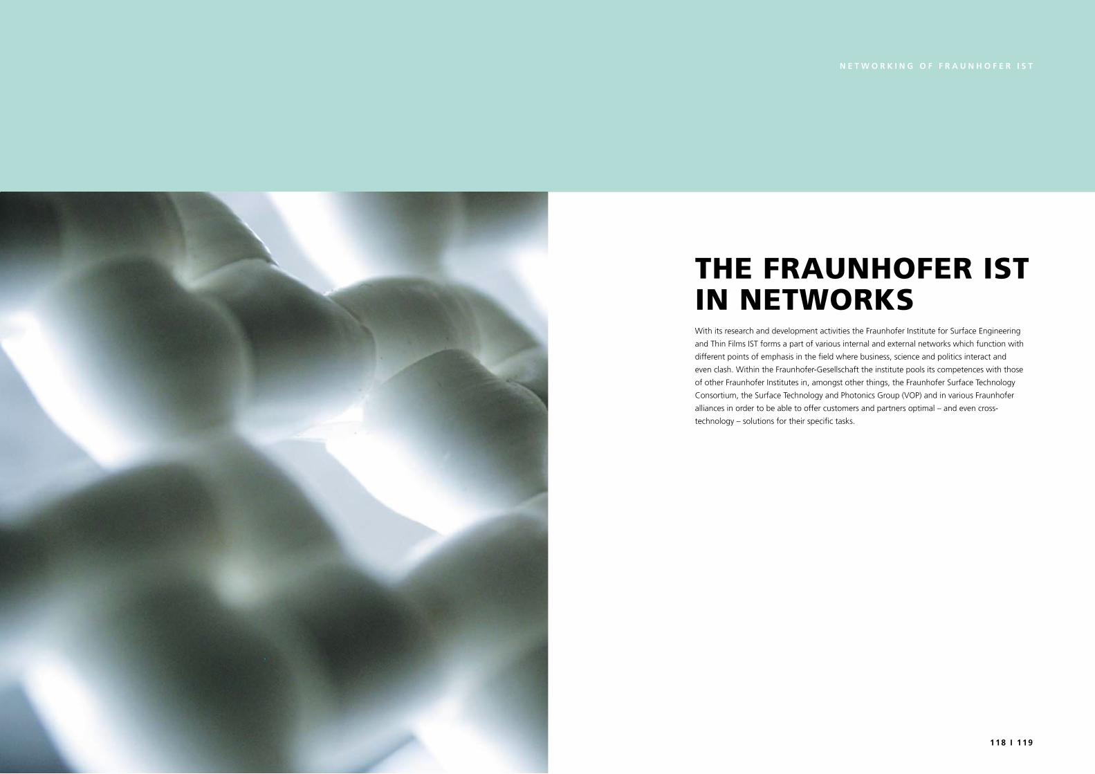
118 I 119
n e T w o r k I n G o F F r a u n h o F e r I S T
With its research and development activities the Fraunhofer Institute for Surface Engineering
and Thin Films IST forms a part of various internal and external networks which function with
different points of emphasis in the field where business, science and politics interact and
even clash. Within the Fraunhofer-Gesellschaft the institute pools its competences with those
of other Fraunhofer Institutes in, amongst other things, the Fraunhofer Surface Technology
Consortium, the Surface Technology and Photonics Group (VOP) and in various Fraunhofer
alliances in order to be able to offer customers and partners optimal – and even cross-
technology – solutions for their specific tasks.
tHe FRAunHoFeR ist in netwoRks

120 I 121
n e T w o r k I n G o F F r a u n h o F e r I S T
With its clearly defined mission of application-oriented
research and its focus on key technologies of relevance to the
future, the Fraunhofer-Gesellschaft plays a prominent role
in the German and European innovation process. Applied
research has a knock-on effect that extends beyond the direct
benefits perceived by the customer: Through their research
and development work, the Fraunhofer Institutes help to re-
inforce the competitive strength of the economy in their local
region, and throughout Germany and Europe. They do so by
promoting innovation, strengthening the technological base,
improving the acceptance of new technologies, and helping to
train the urgently needed future generation of scientists and
engineers.
As an employer, the Fraunhofer-Gesellschaft offers its staff
the opportunity to develop the professional and personal
skills that will allow them to take up positions of responsibility
within their institute, at universities, in industry and in society.
Students who choose to work on projects at the Fraunhofer
Institutes have excellent prospects of starting and developing a
career in industry by virtue of the practical training and experi-
ence they have acquired.
The Fraunhofer-Gesellschaft is a recognized non-profit
organization that takes its name from Joseph von Fraunhofer
(1787–1826), the illustrious Munich researcher, inventor and
entrepreneur.
Research of practical utility lies at the heart of all activities
pursued by the Fraunhofer-Gesellschaft. Founded in 1949, the
research organization undertakes applied research that drives
economic development and serves the wider benefit of society.
Its services are solicited by customers and contractual partners
in industry, the service sector and public administration.
At present, the Fraunhofer-Gesellschaft maintains more
than 80 research units in Germany, including 57 Fraunhofer
Institutes. The majority of the 14,000 staff are qualified
scientists and engineers, who work with an annual research
budget of € 1.4 billion. Of this sum, more than € 1.2 billion
is generated through contract research. Two thirds of the
Fraunhofer-Gesellschaft’s contract research revenue is derived
from contracts with industry and from publicly financed
research projects. Only one third is contributed by the German
federal and Länder governments in the form of base funding,
enabling the institutes to work ahead on solutions to problems
that will not become acutely relevant to industry and society
until five or ten years from now.
Affiliated research centers and representative offices in Europe,
the USA and Asia provide contact with the regions of greatest
importance to present and future scientific progress and
economic development.
tHe FRAunHoFeR-gesellscHAFt At A glAnce
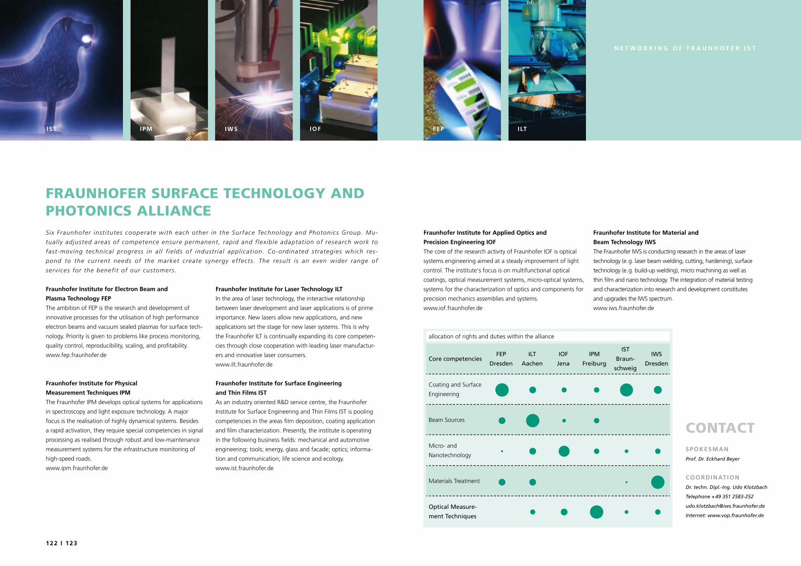
122 I 123
n e T w o r k I n G o F F r a u n h o F e r I S T
Fraunhofer Institute for electron beam and
plasma Technology Fep
The ambition of FEP is the research and development of
innovative pro cesses for the utilisation of high performance
electron beams and vacuum sealed plasmas for surface tech-
nology. Priority is given to problems like process monitoring,
quality control, re pro ducibility, scaling, and profitability.
www.fep.fraunhofer.de
Fraunhofer Institute for physical
measurement Techniques Ipm
The Fraunhofer IPM develops optical systems for applications
in spectroscopy and light exposure technology. A major
focus is the realisation of highly dynamical systems. Besides
a rapid activation, they require special com petencies in signal
processing as realised through robust and low-maintenance
measurement systems for the infrastructure monitoring of
high-speed roads.
www.ipm.fraunhofer.de
Six Fraunhofer inst i tutes cooperate with each other in the Surface Technology and Photonics Group. Mu-
tual ly adjusted areas of competence ensure permanent, rapid and f lex ib le adaptat ion of research work to
fast-moving technical progress in a l l f ie lds of industr ia l appl icat ion. Co-ordinated strategies which res-
pond to the current needs of the market create synergy effects . The result i s an even wider range of
serv ices for the benef i t of our customers.
Fraunhofer Institute for laser Technology IlT
In the area of laser technology, the interactive relationship
between laser development and laser applications is of prime
importance. New lasers allow new applications, and new
applica tions set the stage for new laser sys tems. This is why
the Fraunhofer ILT is continually expanding its core competen-
cies through close cooperation with leading laser manufactur-
ers and innova tive laser consumers.
www.ilt.fraunhofer.de
Fraunhofer Institute for Surface engineering
and Thin Films IST
As an industry oriented R&D service centre, the Fraunhofer
Institute for Surface Engineering and Thin Films IST is pooling
competencies in the areas film deposition, coating application
and film characterization. Presently, the institute is operating
in the follo wing business fields: mechanical and automotive
engineering; tools; energy, glass and facade; optics; informa-
tion and communica tion; life science and ecology.
www.ist.fraunhofer.de
Fraunhofer Institute for applied optics and
precision engineering IoF
The core of the research activity of Fraunhofer IOF is optical
systems engineering aimed at a steady im prove ment of light
control. The insti tute‘s focus is on multifunctional optical
coatings, optical measurement systems, micro-optical systems,
systems for the characterization of optics and components for
precision mechanics assemblies and systems.
www.iof.fraunhofer.de
Fraunhofer Institute for material and
beam Technology IwS
The Fraunhofer IWS is conducting re search in the areas of laser
techno logy (e. g. laser beam welding, cutting, hardening), surface
technology (e. g. build- up welding), micro machining as well as
thin film and nano technology. The integration of material testing
and cha racterization into research and develop ment constitutes
and upgrades the IWS spectrum.
www.iws.fraunhofer.de
FRAunHoFeR suRFAce tecHnologY And pHotonics AlliAnce
contActSpokeSman
Prof. Dr. Eckhard Beyer
CoorDInaTIon
Dr. techn. Dipl.-Ing. Udo Klotzbach
Telephone + 49 351 2583-252
Internet: www.vop.fraunhofer.de
IST Ipm IwS IoF Fep IlT
allocation of rights and duties within the alliance
Core competenciesFEP
Dresden
ILT
Aachen
IOF
Jena
IPM
Freiburg
IST
Braun-
schweig
IWS
Dresden
Coating and Surface
Engineering
Beam Sources
Micro- and
Nanotechnology
Materials Treatment
Optical Measure-
ment Techniques

124 I 125
n e T w o r k I n G o F F r a u n h o F e r I S T
This year a particularly great deal of attention was devoted to
expanding the network within Europe. Initial meetings with
ViaMéca – the French competence network – made it possible
for contacts to be built up with French companies in the field
of machanical engineering. Participation in the international
Intersurfaces conference in France smoothed the way for
further contacts with European networks in the fields of
mechanical and automotive engineering. The first ideas for EU
projects have already been discussed between networks from
Belgium, Spain, Italy, France and Moldavia. A partnership with
ERAI, a service network for international developments, has
enabled us to offer our members support in making contacts
with France.
outlook
One special highlight of the year 2009 will be the “Potentials
in plasma technology” parliamentary soiree to be held in
Berlin in March. The perception and development of the net-
work will be boosted considerably. In addition, more working
groups will be taking up their work in the new year. A new
internet presence will improve service for all interested parties
and for members. Current information and the members area
will be found on the home page at www.inplas.de.
The aim of the INPLAS competence network is to secure and
further extend the global lead of German companies and insti-
tutes in the field of plasma surface finishing technology. Close
networking and bundling of individual activities should make
plasma more familiar as a tool and give it a higher profile both
for the public and in the political arena.
activities in 2008
2008 was a year which brought many innovations but
also consolidations. In addition to a large number of new
members, partners and interested parties enthusiastic about
the INPLAS network, the focus of networking was on the
development of the working groups. The “New kinds of
plasma sources and processes” working group headed by Dr.
Bernhard Cord of Singulus Technologies AG, Kahl am Main,
was able to commence its work successfully. This work group
initiated a workshop on the subject of high power impulse
magnetron sputtering or HiPIMS. Following the workshop,
project concepts were drawn up and new ideas for projects
discussed.
In 2008 as well, INPLAS was once again represented by its
members at a large number of national and international
events and exhibitions. Deserving special mention here are in
particular the ICCG7 conference on glass and plastic coatings
in Eindhoven, and the biggest international conference
on plasma technology in Germany, PSE 2008 in Garmisch-
Partenkirchen.
inplAs – netwoRk oF competence industRiAl plAsmA suRFAce tecHnologY
1 Meeting of the INPLAS-
working group »New
Plasma sources and
processes« under the
direction of Dr. Cord
(Singulus Technologies).
2 Practical demonstration
of HiPIMS-technologies in
the lab.
contActBranch Office INPLAS
INPLAS - Network of Competence
Industrial Plasma Surface Technology
Dipl.-Ing. Carola Brand
Telefon +49 531 21 55-574
Dr. Gerrit von Borries
Telephone +49 531 2155-622
www.inplas.de
1
as of 1.12.2008
126 I 127
pictuRe indexCover picture
Direct laser writing of sensor structures, which are embedded
between tribological insulating layers, for temperature
detection in the track of bearings during work. Picture: Reiner
Meier, Wittmar
S. 2: Ludes Generalplaner GmbH, Berlin
S. 3: Sascha Grammann, Braunschweig
S. 6 1,2: Falko Oldenburg, Braunschweig
S. 8: private
S. 14: Falko Oldenburg, Braunschweig
S. 16; 1-2,5-7,8-17: Reiner Meier, Wittmar
S. 16; 3,7: Sascha Grammann, Braunschweig
S. 20; 2: Reiner Meier, Wittmar
S. 21; 2: Reiner Meier, Wittmar
S. 22: Reiner Meier, Wittmar
S. 26; 1: Falko Oldenburg, Braunschweig
S. 28: Manuela Lingnau, Braunschweig
S. 30; 1: Falko Oldenburg, Braunschweig
S. 32; 1: Falko Oldenburg, Braunschweig
S. 34: Reiner Meier, Wittmar
S. 36; 37: Manuela Lingnau, Braunschweig
S. 42: Falko Oldenburg, Braunschweig
S. 50: Reiner Meier, Wittmar
S. 53; 3: H. Jacobsen, Fraunhofer ISIT
S. 56 1: Falko Oldenburg, Braunschweig
S. 60; 2: Falko Oldenburg, Braunschweig
S. 64: Falko Oldenburg, Braunschweig
S. 66; 1: Falko Oldenburg, Braunschweig
S. 66; 2: Manuela Lingnau, Braunschweig
S. 68; 2: Krees Nagel, Braunschweig
S. 78; 1: Falko Oldenburg, Braunschweig
S. 84: Reiner Meier, Wittmar
S. 86: pixelio - Jörg Trampert
S. 90: Falko Oldenburg, Braunschweig
S.114: Mandalla, photocase.com
All other pictures: Fraunhofer Institute for Surface Engineering
and Thin Films IST, Braunschweig.
memBeRsHipsArbeitskreis Plasmaoberflächentechnologie (AK Plasma)
www.akplasma.de
Competenz-Centrum Ultrapräzise Oberflächenbearbeitung
CC UPOB e. V.
www.upob.de
Deutsche Gesellschaft für Materialkunde e. V.
www.dgm.de
Deutsche Gesellschaft für Galvano- und
Oberflächentechnik e. V.
www.dgo-online.de
Europäische Forschungsgesellschaft Dünne Schichten e. V.
(EFDS)
www.efds.org
European Society for Precision Engineering
and Nanotechnology (euspen)
www.visiononlinde.tv
ForschungRegion Braunschweig e. V.
www.forschungregion-braunschweig.de
Forschungsvereinigung Räumliche Elektronische
Baugruppen 3-D MID e. V.
www.faps.uni-erlangen.de/mid
Fraunhofer-Netzwerk Elektrochemie
Zentrum für Mikroproduktion e. V. (ZemPro)
International Council for Coatings on Glass e. V.
Kompetenznetz Industrielle Plasma-Oberflächentechnik e. V.
(INPLAS)
www.inplas.de
Materials Valley e. V.
www.materials-valley-rheinmain.de
Nanotechnologie-Kompetenzzentrum
“Ultradünne funktionale Schichten”
www.nanotechnology.de
Neue Materialien Niedersachsen e. V. (NMN)
www.nmn-ev.de
PhotonicNet GmbH – Kompetenznetz Optische Technologien
www.photonicnet.de
Fraunhofer-Allianz Photokatalyse
www.photokatalyse.fraunhofer.de
Fraunhofer-Allianz Proteinchips
www.proteinchips.fraunhofer.de
Fraunhofer-Allianz Reinigungstechnik
www.allianz-reinigungstechnik.de
Fraunhofer-Themenverbund Adaptronik
www.adaptronik.fraunhofer.de
Fraunhofer-Themenverbund Numerische Simulation von
Produkten, Prozessen
www.nusim.fraunhofer.de
Fraunhofer-Verbund Oberflächentechnik und Photonik
www.vop.fraunhofer.de

impRintFraunhofer Institute for Surface engineering and Thin
Films IST
Director of the Institute
Prof. Dr. Günter Bräuer
Deputy Director of the Institute
Dipl.-Ing. Wolfgang Diehl
Bienroder Weg 54 E
38108 Braunschweig
Telephone +49 531 2155-0
Fax +49 531 2155-900
www.ist.fraunhofer.de
editorial und coordination:
Dr. Simone Kondruweit
Dipl.-Sozialwiss. Elena Droege
M. A. Anika Heddergott
layout
Dipl.-Des. Falko Oldenburg
Arnold & Domnick, Leipzig
Verlagsproduktion – alle Medien
© Fraunhofer IST 2009