FPGA Implementation of LTE Downlink Transceiver with ... and coding techniques such as the...
11
Communications on Applied Electronics (CAE) – ISSN : 2394-4714 Foundation of Computer Science FCS, New York, USA Volume 2 – No.2, June 2015 – www.caeaccess.org 1 FPGA Implementation of LTE Downlink Transceiver with Synchronization and Equalization Sara M. Hassan Modern Academy, Cairo, Egypt Abdelhalim Zekry Ain Shams University, Cairo, Egypt ABSTRACT Long Term Evolution (LTE) is an advanced standard of the mobile communication systems. LTE has been developed by the 3 rd Generation Partnership Project (3GPP). The new features exhibited by LTE is a direct impact of applying new modulation and coding techniques such as the Orthogonal Frequency Division Multiplexing (OFDM) for the Downlink and the Single Carrier Frequency Division Multiple Access (SC-FDMA) for the Uplink as well as turbo coding. This paper presents a Field Programmable Gate Array (FPGA) design and implementation of the LTE downlink transmitter and receiver according to releases 8 and 9 on Virtex 6 XC6VLX240T FPGA kit using Xilinx® ISE® Design Suite version 12.1. It is found that the utilization of the look up tables and flip plops amounts to about 65 percent while the other logic devices utilization on the chip amount to only 5- 13 percent. Such implementations can be considered as IPs for software defined radios. The information is also useful for the FPGA developers. The most important consequence is that the FPGA vendors may produce more appropriate counts of the resource blocks for better the utilization of the chips used in the LTE transceivers. Keywords LTE, 4G, 3GPP, OFDM, 2G ,3G, LTE downlink physical layer, release 8, release 9 Xilinx Design Suite, virtex 6 XC6VLX240T FPGA. 1. INTRODUCTION The Long Term Evolution (LTE) is an advanced standard for wireless voice and data communication., The 3GPP standards’ body has completed definition of the first release of the LTE system, The main advantages of the LTE, also known as 4G, over the 2G and 3G systems are utilizing a higher peak data rates by providing for an uplink speed of up to 50 megabits per second (Mbps) and a downlink speed of up to 100 Mbps. LTE will bring many technical benefits to cellular NETWORKS. BANDWIDTH WILL BE SCALABLE FROM 1.25 MHZ TO 20 MHz. This will suit the needs of different network operators that have different bandwidth allocations, and also allow operators to provide different services based on spectrum. LTE also improved spectral efficiency up to 5 bps/Hz for Downlink and 2.5 bps/Hz for Uplink, allowing carriers to provide more data and voice services over a given bandwidth. The LTE physical layer (PHY) is a highly efficient means of conveying both data and control information between an enhanced base station (eNodeB) and mobile user equipment (UE). The LTE PHY layer employs some advanced technologies that are new to cellular applications. These include Orthogonal Frequency Division Multiplexing (OFDM) and Multiple Input Multiple Output (MIMO) data transmission. In addition, the LTE PHY layer uses Orthogonal Frequency Division Multiple Access (OFDMA) on the downlink (DL) and Single Carrier – Frequency Division Multiple Access (SC-FDMA) on the uplink (UL). OFDMA allows data to be directed to or from multiple users on a subcarrier-by-subcarrier basis for a specified number of symbol periods. Due to the novelty of these technologies in cellular applications, they are described separately before delving into a description of the LTE PHY layer. LTE uplink requirements differ from downlink requirements in several ways. Not surprisingly, power consumption is a key consideration for UE terminals. The high PAPR and related loss of efficiency associated with OFDM signaling are major concerns. As a result, an alternative to OFDM was sought for use in the LTE uplink. Single Carrier – Frequency Domain Multiple Access (SC- FDMA) is well suited to the LTE uplink requirements. The basic transmitter and receiver architecture is very similar (nearly identical) to OFDMA, and it offers the same degree of multipath protection. Importantly, because the underlying waveform is essentially single-carrier, the PAPR is lower [1- 5]. The continued increase in the number of users of mobile communications all over the world, motivated researchers to search for a unified wireless platform. This will enable the mobile users to conduct business and exchange data easily while moving elsewhere in the world. The new features of LTE made it the promising platform intended for the advancements in mobile communications [6]. In the last few years, technology evolution in mobile communications is mainly motivated by two relevant agents: (1) the market globalization and liberalization and the increasing competence among vendors and operators coming from this new framework, (2) the exponential increase in the demand for advanced telecommunication services and we note that the computational framework and the insights gained via the numerical studies can be extended to other orthogonal division frequency multiple access (OFDMA) technologies, For that the many researchers are concerned with the development of implementation methods and techniques for the building blocks of the LTE physical layer. So, an extensive research work is directed to the implementation of the building blocks of this system using different platforms [7-10]. This paper presents the simulation and the FPGA implementation of the LTE downlink physical layer (on Virtex 6 XC6VLX240T FPGA kit) according to release 9 using Xilinx package version 12.1. Every stage in both the transmitter and receiver are implemented, and verified. The paper is organized such that section 2 presents the full detailed description of the building blocks of the LTE transmitter and
Transcript of FPGA Implementation of LTE Downlink Transceiver with ... and coding techniques such as the...

Communications on Applied Electronics (CAE) – ISSN : 2394-4714
Foundation of Computer Science FCS, New York, USA
Volume 2 – No.2, June 2015 – www.caeaccess.org
1
FPGA Implementation of LTE Downlink Transceiver with
Synchronization and Equalization
Sara M. Hassan Modern Academy,
Cairo, Egypt
Abdelhalim Zekry Ain Shams University,
Cairo, Egypt
ABSTRACT
Long Term Evolution (LTE) is an advanced standard of the
mobile communication systems. LTE has been developed by
the 3rd Generation Partnership Project (3GPP). The new
features exhibited by LTE is a direct impact of applying new
modulation and coding techniques such as the Orthogonal
Frequency Division Multiplexing (OFDM) for the Downlink
and the Single Carrier Frequency Division Multiple Access
(SC-FDMA) for the Uplink as well as turbo coding. This
paper presents a Field Programmable Gate Array (FPGA)
design and implementation of the LTE downlink transmitter
and receiver according to releases 8 and 9 on Virtex 6
XC6VLX240T FPGA kit using Xilinx® ISE® Design Suite
version 12.1. It is found that the utilization of the look up
tables and flip plops amounts to about 65 percent while the
other logic devices utilization on the chip amount to only 5-
13 percent. Such implementations can be considered as IPs for
software defined radios. The information is also useful for the
FPGA developers. The most important consequence is that the
FPGA vendors may produce more appropriate counts of the
resource blocks for better the utilization of the chips used in
the LTE transceivers.
Keywords
LTE, 4G, 3GPP, OFDM, 2G ,3G, LTE downlink physical
layer, release 8, release 9 Xilinx Design Suite, virtex 6
XC6VLX240T FPGA.
1. INTRODUCTION The Long Term Evolution (LTE) is an advanced standard for
wireless voice and data communication., The 3GPP standards’
body has completed definition of the first release of the LTE
system, The main advantages of the LTE, also known as 4G,
over the 2G and 3G systems are utilizing a higher peak data
rates by providing for an uplink speed of up to 50 megabits
per second (Mbps) and a downlink speed of up to 100 Mbps.
LTE will bring many technical benefits to cellular NETWORKS.
BANDWIDTH WILL BE SCALABLE FROM 1.25 MHZ TO 20 MHz.
This will suit the needs of different network operators that
have different bandwidth allocations, and also allow operators
to provide different services based on spectrum. LTE also
improved spectral efficiency up to 5 bps/Hz for Downlink and
2.5 bps/Hz for Uplink, allowing carriers to provide more data
and voice services over a given bandwidth.
The LTE physical layer (PHY) is a highly efficient means of
conveying both data and control information between an
enhanced base station (eNodeB) and mobile user equipment
(UE). The LTE PHY layer employs some advanced
technologies that are new to cellular applications. These
include Orthogonal Frequency Division Multiplexing
(OFDM) and Multiple Input Multiple Output (MIMO) data
transmission. In addition, the LTE PHY layer uses Orthogonal
Frequency Division Multiple Access (OFDMA) on the
downlink (DL) and Single Carrier – Frequency Division
Multiple Access (SC-FDMA) on the uplink (UL). OFDMA
allows data to be directed to or from multiple users on a
subcarrier-by-subcarrier basis for a specified number of
symbol periods. Due to the novelty of these technologies in
cellular applications, they are described separately before
delving into a description of the LTE PHY layer.
LTE uplink requirements differ from downlink requirements
in several ways. Not surprisingly, power consumption is a key
consideration for UE terminals. The high PAPR and related
loss of efficiency associated with OFDM signaling are major
concerns. As a result, an alternative to OFDM was sought for
use in the LTE uplink.
Single Carrier – Frequency Domain Multiple Access (SC-
FDMA) is well suited to the LTE uplink requirements. The
basic transmitter and receiver architecture is very similar
(nearly identical) to OFDMA, and it offers the same degree of
multipath protection. Importantly, because the underlying
waveform is essentially single-carrier, the PAPR is lower [1-
5].
The continued increase in the number of users of mobile
communications all over the world, motivated researchers to
search for a unified wireless platform. This will enable the
mobile users to conduct business and exchange data easily
while moving elsewhere in the world. The new features of
LTE made it the promising platform intended for the
advancements in mobile communications [6].
In the last few years, technology evolution in mobile
communications is mainly motivated by two relevant agents:
(1) the market globalization and liberalization and the
increasing competence among vendors and operators coming
from this new framework, (2) the exponential increase in the
demand for advanced telecommunication services and we
note that the computational framework and the insights gained
via the numerical studies can be extended to other orthogonal
division frequency multiple access (OFDMA) technologies,
For that the many researchers are concerned with the
development of implementation methods and techniques for
the building blocks of the LTE physical layer. So, an
extensive research work is directed to the implementation of
the building blocks of this system using different platforms
[7-10].
This paper presents the simulation and the FPGA
implementation of the LTE downlink physical layer (on
Virtex 6 XC6VLX240T FPGA kit) according to release 9
using Xilinx package version 12.1. Every stage in both the
transmitter and receiver are implemented, and verified. The
paper is organized such that section 2 presents the full detailed
description of the building blocks of the LTE transmitter and

Communications on Applied Electronics (CAE) – ISSN : 2394-4714
Foundation of Computer Science FCS, New York, USA
Volume 2 – No.2, June 2015 – www.caeaccess.org
2
receiver. Section 3 introduces the design verification while
section four gives data about the system utilization of the
Xilinix Vertix 6 and section fie concludes the paper.
2. TRANSIMITTER AND RECIVER
IMPLEMENTATION The LTE implementation in this paper is built according to
specifications of LTE in release 9 with FDD (Frequency
Division Duplex) frame structure. The implemented system
has a carrier bandwidth of 3 GHz, the number of sub-channels
is 15, the number of sub-carrier is 180, the IFFT/FFT size is
256, the turbo encoder/decoder rate is 1/3, and the data input
for one OFDM symbol has a length of 96 bits [11].
Figure 1 and Figure 2 show the implemented transmitter and
receiver block diagrams, respectively. All the operations done
in the transmitter have to be done reversely in the receiver.
The reverse operation of the cyclic redundancy check )CRC (
in the transmitter is the DE-CRC in the receiver , the
segmentation block in the transmitter corresponds to DE-
Segmentation in the receiver , the turbo encoder in the
transmitter corresponds to Decoder in the receiver, the rate
matching block in the transmitter corresponds to De- rate
matching in the receiver, the scrambler in the transmitter
corresponds to De-Scrambler in the receiver, the mapper in
the transmitter corresponds to De-mapper in the receiver , the
inverse Fourier transform block (IFFT) in the transmitter
corresponds to FFT in the receiver, and the cyclic prefix
insertion block in the transmitter corresponds to cyclic prefix
remove in the receiver.
In the following sections, we will show the VHDL model and
FPGA implementation of the basic building blocks of the
transmitter and the corresponding blocks in the receiver.
Moreover, the verification of each block and its reverse
operation will be shown. Finally overall system
(transmitter/receiver) verification will be done.
Fig 1: The blocEk diagram of physical layer of the LTE
downlink transmitter [11]
Fig 2: The receiver block diagram [14]
2.1 CRC and DE-CRC implementation The first block in the transmitter is the CRC; which is an
independent block. The function of this block is to add 24
redundancy bits at the start of each transport block for sake of
detecting errors in the whole transport block. According to the
specifications, the polynomial used in this block is called
“gCRC24A” and it follows the equation [12]:
gCRC24A(D) = [D24 + D23 + D18 + D17 + D14 + D11 + D10 + D7 +
D6 + D5 + D4 + D3 + D + 1].
Where Dn is the location that will be occupied by “1”.
The transport block data is modulo 2 divided by this generator
polynomial of 24 bits sequence and the remainder is the CRC
bit sequence that will be added to the start of the transport
block. This block is modeled using the hardware description
language VHDL and implemented on Xilinix Vertix 6 FPGA
chip. The implementation is validated by assuming an input
data sequence of 25 ones, then the CRC output data must be
‘011110011011001100000100’. Figure 3 shows the results of
the implemented CRC block. It is shown that the number of
input bits to the CRC block is 25 bits. The number of the CRC
bits is 24 bits. Consequently the number of the output bits is
49 (input + CRC bits).
The DE-CRC process is implemented in the receiver. This
process is executed in the same way as in the transmitter
where the received data bits (25 bits) are used to generate 24
CRC bits following the same processing steps that made at the
transmitter. Figure 4 shows the simulation of the DE-CRC
block. The error indicator output flag is zero which means the
CRC-bits regenerated at the receiver is the same as the CRC-
bits generated at the transmitter. This verifies the CRC and
DE-CRC blocks.
Fig 3: The simulation results of the CRC block
Fig 4: The simulation results of the DE-CRC block
2.2 SEGMENTATION and DE-
SEGMENTATION The Turbo Encoder can handle the data correctly if only its
input transport block size is less than 6144. In case the length
of the input transport block is greater than 6144, then the
transport block is split into multiple segments. In this case, a
CRC code is added to every segment to detect the error in it.
The CRC inside the segmented block is calculated according
to a different polynomial than that used previously in the first
CRC block. The CRC generating polynomial used is
called”gCRC24B” and is expressed by the following equation
[12]:

Communications on Applied Electronics (CAE) – ISSN : 2394-4714
Foundation of Computer Science FCS, New York, USA
Volume 2 – No.2, June 2015 – www.caeaccess.org
3
gCRC24B(D) = [D24 + D23 + D6 + D5 + D + 1].
The output of the first CRC block, which comprises 49 bits, is
utilized as an input to the segmentation block. The 49 bits are
segmented into 3 equal segments. The segmentation process is
executed according to the standards of release 9 section
(5.1.2) and the length of each segment is determined
according to table (5.1.3-3) [12]. The simulation results of the
segmentation building block are shown in Figure 5.
The DE-segmentation process is the reverse operation of the
segmentation process, that by reassemble the received
segments at the receiver. The DE segmentation building block
is designed and implemented by a VHDL code and it function
is verified in the same manner as the segmentation block.
Fig 5: The testing results of the segmentation block.
2.3 TURBO ENCODER AND DECODER In the following subsections, we will show the Turbo
Encoder and Decoder implementation and its verification.
2.3.1 Turbo Encoder The third block in the LTE transmitter is the Turbo Encoder.
The Parallel Concatenated Convolutional Code (PCCC) is the
scheme used in the Turbo Encoder. As shown in Figure 6, this
scheme consists of two 8-state encoders and one turbo code
internal interleaver. The coding rate of this turbo encoder is
1/3. The input to the Turbo Encoder is the output of the
Segmentation block; with a length of 100 bits. The three
outputs of the Encoder are the systematic sequence )0(
Kd and
two sequences of parity bits )1(
Kd , and )2(
Kd . The length of each
one of the three outputs is 100 bits. The systematic sequence (
)0(
Kd ) is the same as the input sequence Turbo encoderKc ,
while the two parity sequences of the two parity sequences ()1(
Kd , )2(
Kd ) are calculated according to the logic circuit shown
in Figure 6. In turbo encoder the output sequences of length K
must be terminated by padding 3 consequent zeros to the input
sequence.
Fig 6: Structure of rate 1/3 turbo encoder [11]
Then, the transmitted bits for trellis termination shall then be
[11]:
KK xd )0(
, 1)0(1 KK zd , KK xd
)0(2 , 1
)0(3
KK zd
KK zd )1(
, 2)1(
1 KK xd , KK zd )1(
2 , 2)1(
3 KK xd
1)2(
KK xd , 2)2(1 KK zd , 1
)2(2
KK xd ,
2)2(3
KK zd ,
Where K is the number of input bits.
The turbo encoder is implemented by a Xilinx core. The
results of the implemented turbo encoder generated by Xilinix
core is shown in Figure 7. The input data sequence and the
three outputs (schematic, parity1, and parity2) are clearly seen
in the figure.
Fig 7: The implementation results of the turbo encoder.
2.3.2 The Turbo Decoder The Turbo Decoder process is the reverse operation of the
turbo encoder. The Decoder is implemented by a Xilinx core.
Figure 8 shows the testing results of the implemented decoder.
The three inputs (schematic, parity1, and parity2) and output
data sequences are clearly seen in the Figure.
Fig 8: The simulation results of the decoder
2.3.3 Turbo Encoder and Decoder verification The verification is accomplished by the Loop back test where
the output of the decoder is input to the decoder. The Turbo
Encoder and the Decoder verification is passed when the
output of the Decoder is identical to the input of the Turbo
Encoder. The verification test results of the Encoder and
Communications on Applied Electronics (CAE) – ISSN : 2394-4714
Foundation of Computer Science FCS, New York, USA
Volume 2 – No.2, June 2015 – www.caeaccess.org
4
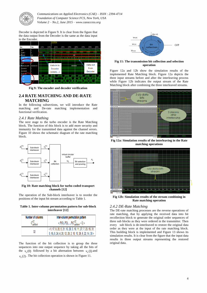
Decoder is depicted in Figure 9. It is clear from the figure that
the data output from the Decoder is the same as the data input
to the Encoder.
Fig 9: The encoder and decoder verification
2.4 RATE MATCHING AND DE-RATE
MATCHING In the following subsections, we will introduce the Rate
matching and De-rate matching implementation and
functional verification.
2.4.1 Rate Mathing The next stage to the turbo encoder is the Rate Matching
block. The function of this block is to add more security and
immunity for the transmitted data against the channel errors.
Figure 10 shows the schematic diagram of the rate matching
block.
Sub-block
interleaver
Sub-block
interleaver
Sub-block
interleaver
Bit
collection
virtual circular
buffer
Bit selection
and pruning
)0(kd
)1(kd
)2(kd
ke
)0(kv
)1(kv
)2(kv
kw
Fig 10: Rate matching block for turbo coded transport
channels [12]
The operation of the Sub-block interleaver is to reorder the
positions of the input bit stream according to Table 1.
Table 1. Inter-column permutation pattern for sub-block
interleaver [12]
The function of the bit collection is to group the three
sequences into one output sequence by taking all the bits of
the )0(kv followed by a bit alternation between )1(kv and
)2(kv . The bit collection operation is shown in Figure 11.
Fig 11: The transmission bit collection and selection
operation
Figure 12a and 12b show the simulation results of the
implemented Rate Matching block. Figure 12a depicts the
three input streams before and after the interleaving process
while Figure 12b indicates the output stream of the Rate
Matching block after combining the three interleaved streams.
Fig 12a: Simulation results of the interleaving in the Rate
matching operations
Fig 12b: Simulation results of the stream combining in
Rate matching operation
2.4.2 DE-Rate Matching The DE-rate matching processes are the reverse operations of
rate matching, that by applying the received data into bit
recollection block to generate the original order sequences of
three sub blocks as they were ordered in the transmitter. Then
every sub block is de-interleaved to restore the original data
order as they were at the input of the rate matching block.
This building block is implemented and Figure 13 shows its
simulation results. It is clear from the figure that the input data
results in three output streams representing the restored
original data.
O/P

Communications on Applied Electronics (CAE) – ISSN : 2394-4714
Foundation of Computer Science FCS, New York, USA
Volume 2 – No.2, June 2015 – www.caeaccess.org
5
Fig 13: Simulation results of DE-Rate matching operations
2.4.3 Rate Matching and DE-Rate Matching
verification The functionality of the Rate Matching and the De-rate
matching blocks are verified by the loop back test where the
output data of the Rate Matching block is directly connected
as an input to the De-rate matching block. Then if they
function correctly the output the De-rate matching must be
identical to the input of the Rate Matching. This test is
executed and the results are illustrated in Figure 14.
Fig 14: The Rate Matching and De-rate Matching
verification
By inspecting the figure it is clear that the three inputs to the
Rate matching block at the transmitter; which are systematic,
parity 1, and parity 2 streams, are the same as the output of
the DE Rate matching block at the receiver.
2.5 THE SCRAMBLER AND DE-
SCRAMBLER 2.5.1 The Scrambler The next stage after turbo encoder is the Scrambler. There are
two main functions for the Scrambler; increasing the system
security and preventing long sequences of ones or zeros in the
transmitted data to facilitate the clock regeneration in the
receiver. The two functions are done through using a Pseudo
Random Sequence Generator (PRSG) having a length of 31
bits that is Xored with the data to produce the Scrambler
output.
Following the same procedure as with the previous building
blocks, The test results of the implemented scrambler is
shown in Figure 15, where “data_in” is the input data to the
Scrambler, “q_out” is the output from the PRSG, and
“data_out” is the output data from Scrambler such that
(data_out = data_in Xor q_out).
Fig 15: The simulation results of the scrambler
2.5.2 The DE- Scrambler The DE-scrambler process is the reverse of the scrambler
process that by Xoring the received data with the “q_out”
sequence, the same one at the transmitter, restores the original
data as that input to the scrambler produces the De-scrambler
output. The test results of the implemented DE-scrambler is
shown in Figure 16, where “data_in” is the received input data
to DE-Scrambler, “q_out” is the output from the PRSG, and
“data_out” is the output data from DE-Scrambler.
Fig 16: The simulation results of the DE-scrambler
2.5.3 Scrambler and DE- Scrambler verification The Scrambler and the Descrambler verification is carried out
by the conventional loop back test where the output of the
descrambler is directly input to the descrambler. If the output
of the descrambler is identical to the input of scrambler, then
the design is correct. Figure 17 depicts the results of the loop
back test where one sees clearly that the output the
Descrambler is identical to the input of the Scrambler. The
Scrambler and Descrambler verification is shown in figure 17.
Fig 17: The scrambler and de scrambler verification
It is shown that the output from the DE scrambler is the same
as the input to the Scrambler.

Communications on Applied Electronics (CAE) – ISSN : 2394-4714
Foundation of Computer Science FCS, New York, USA
Volume 2 – No.2, June 2015 – www.caeaccess.org
6
2.6 THE OFDM BLOCK The next stage after the scrambler is the orthogonal frequency
division multiplexer, OFDM block. The OFDM block
diagram is shown in figure 18. It consists of a mapper, a pilot
generator, a data and pilot insertion block and an IFFT core.
Fig 18: The OFDM block diagram
The Pseudo Random Sequence Generator (PRSG) is built as
the same in the scrambler block. The pilot generator produces
pilot values and save them in a RAM of length 200 words and
width of 22 bits. These pilots are used at the receiver to
estimate the channel transfer characteristics and hence make
channel equalization. Figure 19 shows the generated pilots.
Fig 19: The generated pilots
Both the output data of the Mapper block and the output data
of the Pilot Generator do not arrive at the same time at the
Data and Pilot Insertion Random access memory, RAM. So,
the Delay unit was implemented to solve this problem. Now
we introduce the major sub blocks of the OFDM block.
2.6.1 Mapper The mapper realizes the constellation diagram of the digital
modulation of the type M-QAM with M= 2 , 4, 16, and 64,
where certain logic number is assigned to a baseband symbol
having specific I and Q components, with I and Q the in-phase
and quadrature component, respectively. The RTL Schematic
of the mapper with M=4 is shown in Figure 20 while the
testing results and signals of the QAM mapper are indicated in
Figure 21.
Fig 20: The Mapper RTL Schematic.
Fig 21: Testing results of the QAM mapper
2.6.2 Data and Pilot Insertion sub block The Data & Pilot Insertion block is mainly a RAM of length
256 words and width 22 bits. According to the specifications,
we use total 180 locations, with 150 for mapped data plus 30
pilots, in the middle of the RAM and the remainder locations
will be filled with zeros. The pilots and data are arranged such
that every pilot address is followed by five data addresses.
The testing results of the implemented Data & Pilot Insertion
sub block are shown in Figure 22.
Fig 22: Testing results of the data and pilot insertion sub
block
2.6.3 IFFT and Cyclic Prefix sub block The last two operations in the transmitter increase the
bandwidth efficiency through orthogonality by using the
Inverse Fast Fourier Transform IFFT and preventing the
transmitted symbols from ISI and ICI through the insertion of
Cyclic Prefix CP. Both the IFFT block and the CP block with
the desired specifications are automatically generated by
Xilinx core. For the implementation, 256 IFFT size (38*2
NULLS + 180 data and pilots) was used. Then the output is
256 samples for the IFFT. Figure 23a and 23b show the test
signals the implementation using IFFT Xilinx core. While
Figure 24 shows the implementation of the CP by Xilinx core
according to the specifications. For short CP, one repeats the
last 144 samples at the start of ODFM symbol.

Communications on Applied Electronics (CAE) – ISSN : 2394-4714
Foundation of Computer Science FCS, New York, USA
Volume 2 – No.2, June 2015 – www.caeaccess.org
7
Fig 23a: The input to the IFFT block
Fig 23b: The output from the IFFT block
Fig 24: The Cyclic Prefix process
2.7 THE DE-OFDM BLOCK The DE-OFDM block performs the reverse operations of the
OFDM block which are cyclic prefix removal, FFT, and DE-
mapping. The VHDL implementation of these sub blocks will
be outlined in the next subsection.
2.7.1 Cyclic prefix remove and FFT The Cyclic prefix removal sub block removes the first
repeated 144 samples of the received data. The FFT of the
remaining OFDM symbol is implemented using a Xilinx core.
Figure 25 shows the IFFT and FFT functionality verification
by the loop back process. The IFFT and the FFT blocks are
verified when the output sequence of the FFT is identical to
that at the input of the IFFT. It is clear from the figure that
they are the same.
Fig 25: The IFFT and FFT verification
2.7.2 DE-mapper De-mapper at receiver has reverse functionality of the mapper
at transmitter, so it receives the complex QAM symbols from
the FFT sub block and translates them into logic values in
bits. Here, for 4- QAM every complex symbol represented by
I and Q values, the output will be 2 bits for every symbol.
Figure 26 shows the simulation results of the De-mapper
block.
Fig 26: The simulation results of the De-mapper sub block
2.8 OFDM AND DE-OFDM
VERIFICATION The OFDM and the DE OFDM verification is passed in the
loop back test when the output the DE- OFDM is identical to
the input of the OFDM. Figure 27 shows the verification results. It is clear that the output from the De OFDM at the
receiver is a delayed version of the input to the OFDM at the
transmitter. The delay is due to delay affected by the
transmission channel.
Fig 27: The OFDM and DE OFDM operation outputs.

Communications on Applied Electronics (CAE) – ISSN : 2394-4714
Foundation of Computer Science FCS, New York, USA
Volume 2 – No.2, June 2015 – www.caeaccess.org
8
2.9 Time and Frequency Synchronization
block The function of the Time Synchronization block is to
determine the start of the OFDM symbol, while the function
of the Frequency Synchronization block is to detect any
frequency offset occurred to the carrier due to the channel
effect and the mismatch between the receiver oscillator and
the received carrier frequency.
The construction of the OFDM symbol is exploited for both
Time and Frequency synchronization. We notice that the CP
added at the front of any OFDM symbol is a copy from its CP
tail an illustrated in Figure 28. To determine the start of the
OFDM symbol, we correlated the coming signal with its
delayed copy by the length of the OFDM symbol. The length
of the correlate is one complete CP of 144 samples. To search
for the start of the CP we shift the received symbol by one bit
and repeat the correlation process till we obtain a peak.
Determining the phase of this maximum one gets the
frequency offset of the carrier. Figure 29 illustrates the above
described processes carried out for Frequency and Timing
synchronization are done through the cross correlation process
where the received OFDM symbols are delayed by the OFDM
symbol time T , conjugated and complex multiplied by the
directly received signal. The output is integrated on the length
of the cyclic prefix T0. The point of interest is that where a
maximum output is reached. From evaluating the phase of the
maximum, one determine the frequency shift of the carrier.
Fig 28: OFDM symbol
Fig 29: Frequency and Timing Synchronization through
cross correlation
VHDL codes for all of the processes in figure 29 are written
and the output of the frequency synchronization operation is
shown in Figure 30. By inspecting the figure we see that the
frequency offset is zero because the channel is modeled only
by a time delay only.
Fig 30: The frequency synchronization operation
The result of the time synchronization operation is shown in
Figure 31. One notices that the start of the OFDM symbol is
detected at sample number 144 as it should be.
Fig 31: The time synchronization operation
2.10 CHANNEL ESTIMATION The Channel Estimation and equalization block is used to
calculate the frequency and phase response of the channel to
correct for the effects of the channel impairments due to Path
Loss, Multi-path Propagation Fading, and Doppler Effect on
the transmitted information in order to recover the transmitted
data correctly.
The main building sub blocks of the Channel Estimation are
shown in Figure 32. It consists of the sub blocks; Estimations
of pilots sub channels, Frequency and time interpolations and
Equalization.
Fig 32: Channel Estimation and equalization general
block diagram
The input to the Estimation of Pilots sub Channels block is
the Real and Imaginary values of pilots after the channel and
the outputs are the Amplitude and phase of the channel
response at pilot position. These Real and Imaginary values
are converted to the polar form using the CORDIC.
We divide the amplitude of the received Pilots by the
amplitude of the original pilot, generated in the receiver, and
subtract the Phase of the original pilot from the Phase of the
received one.
Communications on Applied Electronics (CAE) – ISSN : 2394-4714
Foundation of Computer Science FCS, New York, USA
Volume 2 – No.2, June 2015 – www.caeaccess.org
9
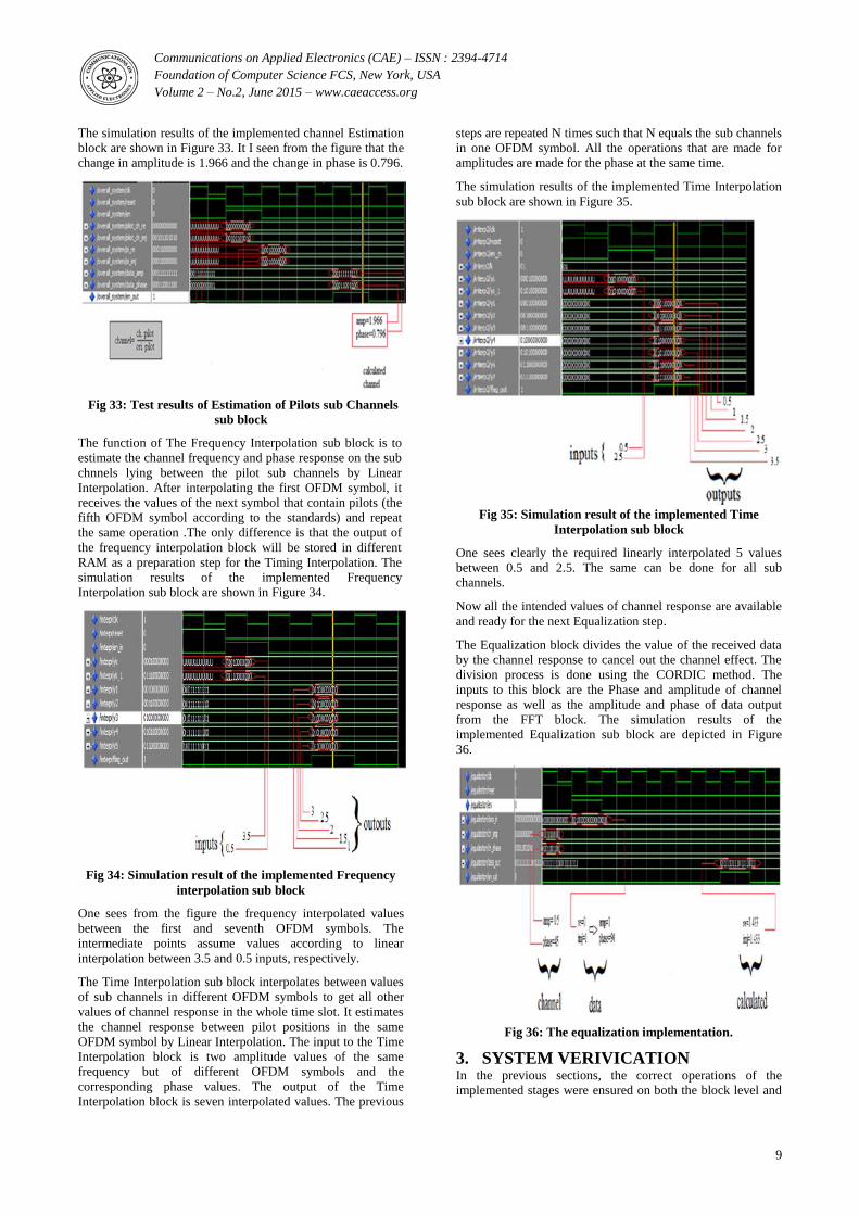
The simulation results of the implemented channel Estimation
block are shown in Figure 33. It I seen from the figure that the
change in amplitude is 1.966 and the change in phase is 0.796.
Fig 33: Test results of Estimation of Pilots sub Channels
sub block
The function of The Frequency Interpolation sub block is to
estimate the channel frequency and phase response on the sub
chnnels lying between the pilot sub channels by Linear
Interpolation. After interpolating the first OFDM symbol, it
receives the values of the next symbol that contain pilots (the
fifth OFDM symbol according to the standards) and repeat
the same operation .The only difference is that the output of
the frequency interpolation block will be stored in different
RAM as a preparation step for the Timing Interpolation. The
simulation results of the implemented Frequency
Interpolation sub block are shown in Figure 34.
Fig 34: Simulation result of the implemented Frequency
interpolation sub block
One sees from the figure the frequency interpolated values
between the first and seventh OFDM symbols. The
intermediate points assume values according to linear
interpolation between 3.5 and 0.5 inputs, respectively.
The Time Interpolation sub block interpolates between values
of sub channels in different OFDM symbols to get all other
values of channel response in the whole time slot. It estimates
the channel response between pilot positions in the same
OFDM symbol by Linear Interpolation. The input to the Time
Interpolation block is two amplitude values of the same
frequency but of different OFDM symbols and the
corresponding phase values. The output of the Time
Interpolation block is seven interpolated values. The previous
steps are repeated N times such that N equals the sub channels
in one OFDM symbol. All the operations that are made for
amplitudes are made for the phase at the same time.
The simulation results of the implemented Time Interpolation
sub block are shown in Figure 35.
Fig 35: Simulation result of the implemented Time
Interpolation sub block
One sees clearly the required linearly interpolated 5 values
between 0.5 and 2.5. The same can be done for all sub
channels.
Now all the intended values of channel response are available
and ready for the next Equalization step.
The Equalization block divides the value of the received data
by the channel response to cancel out the channel effect. The
division process is done using the CORDIC method. The
inputs to this block are the Phase and amplitude of channel
response as well as the amplitude and phase of data output
from the FFT block. The simulation results of the
implemented Equalization sub block are depicted in Figure
36.
Fig 36: The equalization implementation.
3. SYSTEM VERIVICATION In the previous sections, the correct operations of the
implemented stages were ensured on both the block level and

Communications on Applied Electronics (CAE) – ISSN : 2394-4714
Foundation of Computer Science FCS, New York, USA
Volume 2 – No.2, June 2015 – www.caeaccess.org
10
on the system level. The verification on the block level is
done for the main building blocks. If the output of a certain
block in the receiver is the same as the input to the
corresponding block in the transmitter, then the
implementation of these two block pairs is verified. Also, if
the final output of the receiver is a delayed version of the
input of the transmitter after adding the channel effect; which
is represented by a delay of 5μ sec, then the operation of the
overall system is verified.
The overall system verification
All building blocks of the transmitter are integrated together
to build the whole transmitter and the same is carried out for
the receiver. The overall system is schematically shown in
Figure 37 with a transmission channel having a delay of 5
microseconds. The overall system verification was done by
comparing the transmitter input to the receiver output. The
input to the transmitter is two OFDM symbols. Figure 38
shows the input data to the Transmitter while Figure 39 shows
the output of the Receiver. It is noticed that the data output
from the receiver is the same as the data input to transmitter
after a delay of 5 μs of the channel.
Fig 37: The overall transceiver system block diagram
Fig 38: The transmitter input
Fig 39: The receiver output
4. THE SYSTEM UTALIZATION After implementing the whole transceiver on Xilinx Virtex 6 ,
it is interesting to get out the chip utilization for the
transmitter and for the whole system.
4.1 THE TRANSMITTER UTALIZATION The Transmitter utilizes the resources given in Table 2 from
the Virtex 6 FPGA. It is clear from the table that the LTE
transmitter physical layer utilizes a small fraction of resource
blocks from Virtex 6.
Table 2. The Transmitter utilization on Virtex 6
4.2 THE FULL SYSTEM UTALIZATION The full system Transmitter and receiver resources utilization
table from Virtex 6 FPGA is shown in Table 3. It is clear from
the table that the LTE physical layer utilizes a small fraction
of resource blocks from Virtex 6 except the lookup tables plus
FF pairs where their utilization amount to 62 percent much
greater than the other logic blocks. The chip can
accommodate more building blocks to complete the control
layers of the systems. One may modify the design of the
FPGA chips to contain more look up tables more the other
logic blocks to equalize the utilization of all blocks and make
better utilization of the chip resources. One may redesign
system to more equalization of the utilization of the resources
on FPGAs. It is anticipated that thi result is useful and very
important for the FPGA vendors and logic designers.
Table 3. The Full System Utilization on Virtex 6
5. CONCLUSION In this paper a complete LTE base band transceiver has been
designed as a future mobile technology to cope with next user
requirements. All the stages of the LTE Release 9 downlink
physical layer including the transmitter and the receiver are
modeled using Xilinx® ISE® Design Suite version 12.1 and
implemented on Virtex 6 XC6VLX240T FPGA kit. The
implemented building blocks include the synchronization and
equalization function in the receiver. It is found that the whole
LTE downlink physical layer consumes a small fraction of the
all logic blocks except the lookup tables and the pair. Their
utilization amounts to 62 percent much higher than the other
logic resources on the chip. The chip can accommodate more
building blocks to complete the control layers of the systems.
One may modify the design of the FPGA chips to contain
more look up tables more than the other logic blocks to
equalize the utilization of all blocks and make better
utilization of the chip resources. One may redesign the system
for more equalization of the utilization of the resources on
FPGAs. It is anticipated that this result is useful and very
important for the FPGA vendors and logic designers.
6. FUTURE WORK Future work is aimed to perform the complete LTE physical
layer implementation, including the uplink scenario and
focusing on the ongoing changes in the LTE specification
process; the enhancement can be done with the LTE-advanced
starting with Release 10 Specifications.

Communications on Applied Electronics (CAE) – ISSN : 2394-4714
Foundation of Computer Science FCS, New York, USA
Volume 2 – No.2, June 2015 – www.caeaccess.org
11
7. REFERENCES [1] Jim Zyren,Wes McCoy, “Overview of the 3GPP Long
Term Evolution Physical Layer”, White Paper, freescale
semiconductor.
[2] Y. Tsai. G. Zhang. D. Grieco. F. Ozluturk, “Cell Search
in 3GPP Long Term Evolution Systems”, IEEE
Vehicular Technol. Magazine, vol.2, no.2, June 2007,
pp.23-29.
[3] Rohde Schwarz, “UMTS Long Term Evolution (LTE)
Technology Introduction”, Rohde Schwarz, Application
Note 1MA111, Sep. 2008.
[4] Motorola, Inc.,” Long Term Evolution (LTE): A
Technical Overview”, Motorola, Inc., Technical
White Paper, 2007.
[5] S. Maruyama, S. Ogawa, K. Chiba, “Mobile Terminals
toward LTE and Requirements on Device Technologies”,
IEEE Symposium on VLSI circuit, pp. 2-5, June 2007.
[6] “LTE: The Future of Mobile Broadband Technology”,
white paper, Verizon wireless.
[7] LTE; Evolved Universal Terrestrial Radio Access (E-
UTRA); Physical channels and modulation (3GPP TS
36.211 version 8.3.0 Release 8), ETSI TS 136 211
V8.3.0 (2008-11), Technical Specification.
[8] Sung-won Kim, Kun-yong Kim, “Physical layer
verification for 3GPP LTE (FDD)”, Agilent
Technologies.
[9] Christian Mehlf• uhrer, Martin Wrulich, Josep Colom
Ikuno, Dagmar Bosanska, Markus Rupp “SIMULATING
THE LONG TERM EVOLUTION PHYSICAL
LAYER”, 17th European Signal Processing Conference
(EUSIPCO 2009).
[10] A.Manikandan,V.Venkataramanan, M.Kavitha,
S.Parvathi,” PERFORMANCE ANALYSIS OF LTE
PHYSICAL LAYER BASED ON RELEASE 8&9
THROUGH SIMULINK ENVIRONMENT”,
International Journal of Advanced Technology &
Engineering Research (IJATER).
[11] 3rd Generation Partnership Project; Technical
Specification Group Radio Access Network; Evolved
Universal Terrestrial Radio Access (E-UTRA); Physical
Channels and Modulation, Release 9, 3GPP TS 36.211
V9.0.0 (2009-12), Technical Specification.
[12] 3rd Generation Partnership Project Technical
Specification Group Radio Access Network; Evolved
Universal Terrestrial Radio Access (E-UTRA) );
Multiplexing and channel coding (Release 9), 3GPP TS
36.212 V9.4.0 (2011-09), Technical Specification.
8. AUTHOR’S PROFILE Sara M. Hassan was born in Cairo, Egypt, on September 8,
1985. She received the B.Sc. degree in Electrical Engineering
from Modern academy for engineering and technology, Cairo,
Egypt, in 2007, and the M. Sc. degree in Advanced Mobile
Communication Techniques from Ain Shams University,
Cairo, Egypt, in 2013.She is currently a PhD. student in the
Department of Electronics and Communications Engineering
at Ain Shams University. Her general research interests
include design and implementation for Building Blocks in
Advanced Mobile Communication Techniques, and currently
her research work focuses on LTE-Advanced transceivers.
Abdelhalim Zekry is a professor of electronics at faculty of
Engineering, Ain Shams University, Egypt. He worked as a
staff member on several universities. He published more than
160 papers. He also supervised more than 70 Master thesis
and 25 Doctorate. Prof. Zekry focuses his research programs
on the field of microelectronics and electronic applications
including communications and photovoltaics. He got several
prizes for his outstanding research and teaching performance.