FABRICATION AND CHARACTERIZATION OF MOLECULAR SPINTRONICS ...
221
University of Kentucky University of Kentucky UKnowledge UKnowledge University of Kentucky Doctoral Dissertations Graduate School 2008 FABRICATION AND CHARACTERIZATION OF MOLECULAR FABRICATION AND CHARACTERIZATION OF MOLECULAR SPINTRONICS DEVICES SPINTRONICS DEVICES Pawan Tyagi University of Kentucky, [email protected] Right click to open a feedback form in a new tab to let us know how this document benefits you. Right click to open a feedback form in a new tab to let us know how this document benefits you. Recommended Citation Recommended Citation Tyagi, Pawan, "FABRICATION AND CHARACTERIZATION OF MOLECULAR SPINTRONICS DEVICES" (2008). University of Kentucky Doctoral Dissertations. 614. https://uknowledge.uky.edu/gradschool_diss/614 This Dissertation is brought to you for free and open access by the Graduate School at UKnowledge. It has been accepted for inclusion in University of Kentucky Doctoral Dissertations by an authorized administrator of UKnowledge. For more information, please contact [email protected].
Transcript of FABRICATION AND CHARACTERIZATION OF MOLECULAR SPINTRONICS ...
University of Kentucky University of Kentucky
UKnowledge UKnowledge
University of Kentucky Doctoral Dissertations Graduate School
2008
FABRICATION AND CHARACTERIZATION OF MOLECULAR FABRICATION AND CHARACTERIZATION OF MOLECULAR
SPINTRONICS DEVICES SPINTRONICS DEVICES
Pawan Tyagi University of Kentucky, [email protected]
Right click to open a feedback form in a new tab to let us know how this document benefits you. Right click to open a feedback form in a new tab to let us know how this document benefits you.
Recommended Citation Recommended Citation Tyagi, Pawan, "FABRICATION AND CHARACTERIZATION OF MOLECULAR SPINTRONICS DEVICES" (2008). University of Kentucky Doctoral Dissertations. 614. https://uknowledge.uky.edu/gradschool_diss/614
This Dissertation is brought to you for free and open access by the Graduate School at UKnowledge. It has been accepted for inclusion in University of Kentucky Doctoral Dissertations by an authorized administrator of UKnowledge. For more information, please contact [email protected].
ABSTRACT OF DISSERTATION
Pawan Tyagi
The Graduate School
University of Kentucky
2008

FABRICATION AND CHARACTERIZATION OF MOLECULAR SPINTRONICS DEVICES
_______________________________________
ABSTRACT OF DISSERTATION _______________________________________
A dissertation submitted in partial fulfillment of the requirements for the degree of Doctor of Philosophy in the
College of Engineering at the University of Kentucky
By Pawan Tyagi
Lexington, Kentucky
Director: Dr. Bruce J. Hinds, William Bryan Professor of Materials Engineering
Lexington, Kentucky
2008
Copyright © Pawan Tyagi 2008
ABSTRACT OF DISSERTATION
FABRICATION AND CHARACTERIZATION OF MOLECULAR
SPINTRONICS DEVICES
Fabrication of molecular spin devices with ferromagnetic electrodes coupled with a high
spin molecule is an important challenge. This doctoral study concentrated on realizing a novel
molecular spin device by the bridging of magnetic molecules between two ferromagnetic metal
layers of a ferromagnetic-insulator-ferromagnetic tunnel junction on its exposed pattern edges. At
the exposed sides, distance between the two metal electrodes is equal to the insulator film
thickness; insulator film thickness can be precisely controlled to match the length of a target
molecule. Photolithography and thin-film deposition were utilized to produce a series of tunnel
junctions based on molecular electrodes of multilayer edge molecular electrodes (MEME) for the
first time. In order to make a microscopic tunnel junction with low leakage current to observe the
effect of ~10,000 molecules bridged on the exposed edge of a MEME tunnel barrier, growth
conditions were optimized; stability of a ~2nm alumina insulator depended on its ability to
withstand process-induced mechanical stresses. The conduction mechanism was primarily 1)
tunneling from metal electrode to oranometalic core by tunneling through alkane tether that acts
as a tunnel barrier 2) rapid electron transfer within the oranometalic Ni-CN-Fe cube and 3)
tunneling through alkane tether to the other electrode. Well defined spin-states in the
oranometalic Ni-CN-Fe cube would determine electron spin-conduction and possibly provide a
mechanism for coupling.
MEME with Co/NiFe/AlOx/NiFe configurations exhibited dramatic changes in the
transport and magnetic properties after the bridging of oranometalic molecular clusters with S=6
spin state. The molecular cluster produced a strong antiferromagnetic coupling between two

ferromagnetic electrodes to the extent, with a lower bound of 20 erg/cm,2 that properties of
individual magnetic layers changed significantly at RT. Magnetization, ferromagnetic resonance
and magnetic force microscopy studies were performed. Transport studies of this configuration of
MEME exhibited molecule-induced current suppression by ~6 orders by blocking both molecular
channels and tunneling between metal leads in the planar 25μm2 tunnel junction area. A variety of
control experiments were performed to validate the current suppression observation, especially
critical due to observed corrosion in electrochemical functionalization step. The spin devices
were found to be sensitive to light radiation, temperature and magnetic fields.
Along with the study of molecular spin devices, several interesting ideas such as ~9%
energy efficient ultrathin TaOx based photocell, simplified version of MEME fabrication, and
chemical switching were realized. This doctoral study heralds a novel molecular spin device
fabrication scheme; these molecular electrodes allow the reliable study of molecular components
in molecular transport.
KEYWORDS: Molecular Spintronics; Magnetic Tunnel Junctions; Molecular Electronics;
Photovoltaic Cell; Spin Transport; Magneto Resistance.
Pawan Tyagi
10th April, 2008

FABRICATION AND CHARACTERIZATION OF MOLECULAR SPINTRONICS DEVICES
By
Pawan Tyagi
Lexington, Kentucky
Dr. Bruce J. Hinds Director of Dissertation
Dr. Douglass Kalika Director of Graduate Studies
Date: 10th April, 2008

RULES FOR THE USE OF DISSERTATIONS
Unpublished dissertations submitted for the Doctor's degree and deposited in the University of Kentucky Library are as a rule open for inspection, but are to be used only with due regard to the rights of the authors. Bibliographical references may be noted, but quotations or summaries of parts may be published only with the permission of the author, and with the usual scholarly acknowledgements. Extensive copying or publication of the dissertation in whole or in part also requires the consent of the Dean of the Graduate School of the University of Kentucky. A library that borrows this dissertation for use by its patrons is expected to secure the signature of each user. Name Date

DISSERTATION
Pawan Tyagi
The Graduate School
University of Kentucky
2008

FABRICATION AND CHARACTERIZATION OF MOLECULAR SPINTRONICS DEVICES
_______________________________________
DISSERTATION _______________________________________
A dissertation submitted in partial fulfillment of the requirements for the degree of Doctor of Philosophy in the
College of Engineering at the University of Kentucky
By Pawan Tyagi
Lexington, Kentucky
Director: Dr.Bruce J. Hinds, William Bryan Professor of Materials Engineering
Lexington, Kentucky
2008
Copyright © Pawan Tyagi 2008

This doctoral study is dedicated to my beloved family members: My grand father late Ramanand Tyagi
My father Raj Bahadur Tyagi
My mother Chanderwati Tyagi
& my wife Punam Tyagi
iii
ACKNOWLEDGEMENTS
This doctoral study has been possible due to many persons who directly and indirectly
helped me progress in the right direction. In the first place, I am deeply grateful to Prof. Bruce J.
Hinds for granting me an exciting PhD topic and for mentoring the subsequent research efforts. I
respectfully appreciate his role in honing my experimental and analytical skills, giving me
freedom to try new ideas and patiently supporting me during numerous struggles. I had a deeply
satisfying learning period in his lab. I am thankful to the Air Force Office of Scientific Research
and Kentucky Science and Engineering Foundation (KSEF-621-RDE-006 and KSEF-992-RDE-
008) for funding this thesis work.
Thanks are due to administrators and staff of Center of Nanoscience and Engineering. I
am grateful to an accomplished technician late Mr. George Spiggle, for his invaluable role in
accomplishing the critical experiments.
I would like to take the opportunity to thank Prof. Stephen Holmes and Dr. Dong Feng Li
for the synthesis of excellent molecular compounds. I am indebted to my lab mate, Mr. Bing Hu,
for his conscientious help and camaraderie. I am grateful to Prof. Gang Cao, Dr. Vinobalan
Durairaj and Ms. Shalinee Chikara for help with insightful magnetization studies. It is an
immense pleasure to thank Prof. A.F. Miller for training me on FMR setup and giving me access
to her lab. Appreciations are due to Dr. Hequing Huang and Dr. Song for equipping me with
much needed knowledge of AFM. I am indebted to Prof. J. Todd Hasting for numerous insightful
suggestions and help with spectroscopic ellipsometry. I like to thank Mr. Peng-Leen Ong for help
with the transport and capacitance study. Sincere thanks are due to Prof. Kwok Wei Ng for
guidance with low temperature studies and for sparing time to visit our lab to check our setup. I
wish to thank Prof J. K. Lumpp for numerous insightful suggestions about wire-bonding. I
express my thanks to Prof. John Balk for several astute suggestions about mechanical stress
measurements and for giving me access to his sputtering machine.
I express my thanks to the writing center staff at W.T.Young library for refining the
quality of this dissertation.
I gratefully acknowledge time spared by Prof. Ganpathy Murthy, Prof. Lance DeLong,
Prof. Bruce Apanhar, Prof. Supriyo Datta, Prof. Mark Ratner, Prof. Christian Joachim, Prof
Matthew Foulkes, Prof. David Cepereley, Prof. Mark S. Hybertsen, Prof. Igor Zutic, Prof. Sam
Bader, Prof. Ivan Schuller, Prof. J.M.D. Coey and Prof. Arthur J. Epstein for giving their opinions
and suggestions about some of the complex results we observed during this doctoral study.

iv
I am thankful to former lab mate Dr. Nitin Chopra for introducing me to Prof. Hinds.
Much assistance and a vibrant lab environment produced by the company of Mr. Dinesh
Kalyansundaram, Dr. Mainak Mazumdar, Dr. Kerin Keis, Dr. Wu Ji, Ms. Karen Gerstandt, Mr.
Xin Zhan, and Mr. Xin Xu are much appreciated.
I take pleasure in acknowledging Dr. Anjali Mishra, Dr. Mridu Pawan Deka, Ms.
Shalinee Chikara, and Mr. Rupak Datta for making mine and my family’s stay in Lexington
during this Ph.D a pleasant experience.
I am indebted to a number of friends who have assisted me in several crucial stages. I
thank Rahul Kasat for his moral boosting and practical suggestions. I am honored to acknowledge
my friends Mr. Amit Guliani, Dr. Prashant Salwan, Mr. Anand Tiwari, Mr. Ravi Yadav and Mr.
Vivek Bhatnagar for their support during my trying time. I thank Mr. Rahul Srivastava for
helping me get a great learning opportunity at Midhani. I am grateful to Mr. and Mrs. Srivastava,
and their family for providing me a home away from home during my stay in Hyderabad.
It is an immense delight for me to express gratitude to my past teachers who played key
roles in motivating me to choose a research career. Firstly, I would like to thank my high school
teacher, Mr. Bansi Lal Bagla, for showing me the right direction. I am deeply grateful to the late
Prof. A.K. Patwardhan for restoring my interest in research through his excellent teaching and
encouragement during my undergraduate study. I thank Prof. A. K. Pant for helping me to
explore my potential. I would like to thank the mentors of my master program, Prof. R.
Balasubramanium and Prof. Deepak Gupta, for their role in improving my writing and
experimental skills. These skills provided a strong foundation I always benefited from.
I wish to thank my special friend and wife, Dr. Punam Tyagi, for her continuous support,
understanding and taking extra burden; without her mental and emotional support. I am thankful
to my little angel Pranshu Tyagi to bear my long absence from home. I could have not progressed
significantly. I thank my in-laws, Mr. Nakli Ram Tyagi and Mrs. Rajeshwari Tyagi, for their
mental support and blessings.
I wish to express my respect and gratitude to my grandfather and my childhood friend,
Mr. Ramanand Tyagi, who helped me secure my first book for the engineering entrance exam.
Finally, I thank my revered father, Mr. Raj Bahadur Tyagi, and my beloved mother, Mrs.
Chanderwati Tyagi. I express my gratefulness towards my parents for the struggle they
encountered in getting me this far.
v
TABLE OF CONTENTS
Acknowledgements…………..………………………………………………………iii
List of Tables………….……………………………………………………………...ix
List of Figures ………………………………………………………………………..x
List of Files…………………………………………………………………………..xx
Preface.…………………………………………………………………..…………..xxi
Chapter1: Introduction...................................................................................................1
1.1 Spin-independent molecular conduction mechanisms…………………………....2
1.1.1 Molecules behaving as tunnel barriers between two electrodes…..……….4
1.1.2 Molecule behaving as a quantum dot ……………………………..............6
1.1.2.1 Effect of molecular electrode environment on molecular energy
level…………………………………………………..…………6
1.1.2.1.1 Reduction in the charging energy………….............7
1.1.2.1.2 Loss of charge neutrality …………………………..8
1.1.2.1.3 Broadening of molecular levels………….................9
1.1.2.2 Electron dynamics through molecular quantum dots…………...10
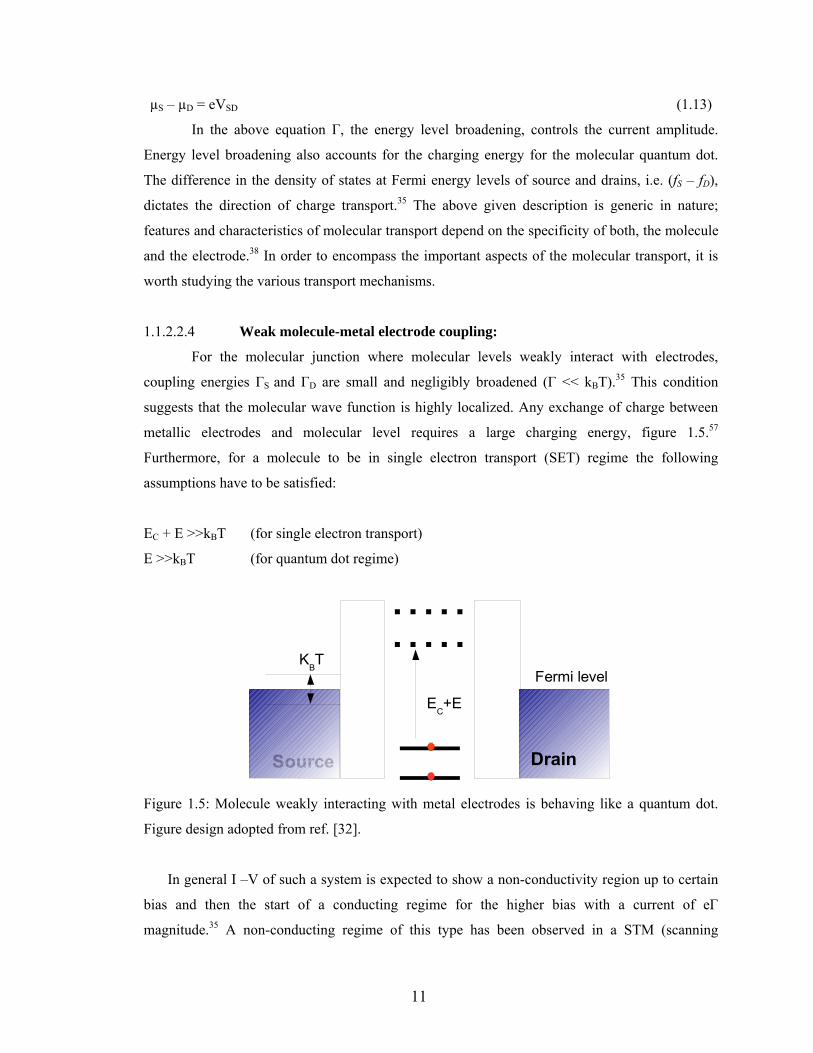
1.1.2.2.1 Weak molecule-metal electrode coupling………...11
1.1.2.2.2 Strong molecule-metal electrode coupling……….12
1.1.2.2.3 Effect of the molecular structure on the molecular
transport mechanism……………………………………….13
1.2 Spin-valves and role of the spin in the molecular transport……………………..19
1.3 Molecular electrode design for molecular spintronics...………………………...33
Chapter 2: Mechanical Stress Control for the Fabrication of Stable Molecular Electrodes at the
Patterned Edges of Metal/Insulator/Metal Junctions…………………………....35
2.1 Introduction……………………………………………………………………...35
2.2 Experimental details……………………………………………………………..37

vi
2.3 Results and discussion…………………………………………………………..40
2.4 Conclusion………………………………………………………………………47
Chapter 3: Molecular Electrodes at the Exposed Edge of Metal-Insulator-Metal Trilayer
Structures…………………………………………………………………….…..48
3.1 Introduction……………………………………………………………………...48
3.2 Physical Methods………………………………………………………………..50
3.3 Results and Discussions
3.3.1 Molecules on Ion-Milled Molecular Electrodes with Atomically Sharp Exposed
Edges …………………………………………………………………….55
3.3.2 Molecules on Photolithography-Liftoff Produced
Molecular Electrodes……………………………………………………..56
3.3.2.1 Control experiments………………………………………………58
3.4 Analysis of Electron Transport via Simmons Tunneling Model………………..61
3.5 Conclusions……………………………………………………………………...67
Chapter 4: Molecular Scale Electrodes Fabricated By Single Step Oxidation of
Photolithographically Defined Metal Electrodes……………………………….68
4.1 Introduction……………………………………………………………………..68
4.2 Experimental Details…………………………………………………………....70
4.3 Results and discussion…………………………………………………………..73
4.3.1 Control experiments………………………………………………………75
4.3.2 Transport-Analysis………………………………………………………..76
4.4 Conclusion………………………………………………………………………78
Chapter 5: TaOx Thin Film Photovoltaic Devices ………………………………………….79
5.1 Introduction……………………………………………………………………..79
5.2 Experimental details………………………………………………………..…...80
5.3 Results and discussion…………………………………………………………..82
5.4 Conclusion………………………………………………………………………90

vii
Chapter 6: Molecular Cluster Induced Antiferromagnetic Coupling between Two Ferromagnetic
Electrodes.……………………………………………………………….…….91
6.1 Introduction…….………………………………………………………….…...91
6.2 Experimental details…………………………………………………………...93
6.3 Results and discussion…………………………………………………………96
6.4 Conclusion……………………………………………………………………113
Chapter 7: Dramatic Current Suppression and Magnetic Ordering Induced By Molecular
Junctions………………………………………………………………………..115
7.1 Introduction…………………………………………………………………...115
7.2 Device fabrication and physical characterization…………………………….117
7.3 Transport measurement methods and apparatus………………………….…..119
7.4 Results……………………………………………………………………….. 120
7.4.1 Control experiments…………………………………………………….121
7.4.1.1 Statistical Observation of F-MEME Current Reduction after
Molecular Attachment………………………………………...122
7.4.1.2 Molecular Reach vs. Tunnel Barrier Thickness………………..124
7.4.1.3 Device current state with 1, 20-Dithioeicosane treatment……..125
7.4.1.4 Electrode composition and molecular junction transport
behavior..……………………………………………………125
7.4.1.5 Chemical and Oxidative Stability of F-MEMEs……………….127
7.4.1.6 Quality of exposed edge of F-MEME for molecule attachment (Ion
Milling vs. Lift-off based F-MEME Fabrication)...…………...127
7.4.1.7 Bottom electrode stability……………………………………...128
7.4.2 Effect of temperature light and magnetic field:
7.4.2.1 Effect of temperature…………………………………………..130
7.4.2.2 Effect of light…………………………………………………..131
7.4.2.3 Effect of magnetic field………………………………………..133

viii
7.4.3 MFM and magnetization study………………………………………....135
7.5 Discussion………………………………………………………………….….137
7.6 Conclusion………………………………………………………………….....143
Chapter 8: Conclusions and Future Work…………………………………………………...144
Appendices………………………………………………………………………………..….151
Appendix A1: Key parameters for reproducing multilayer edge molecular electrodes…..…151
Appendix A2: Stability of bottom metal layers…………………………………………..….155
Appendix A3: Fabrication of semiconductor-molecule-metal junction using multilayer edge
molecular electrode design…………………… ……………………….…..163
Appendix A4: Conducting probe AFM study of magnetic molecular cluster self assembled on
NiFe…………………………………………………………………………164
Appendix A5: Magnetization study of NiFe/AlOx/Pd, TaCoNiFe/AlOx/Pd, NiFe and
Ta/Co/NiFe with and without treatment with organometallic cluster………165
Appendix A6: Molecular spin device with different configurations of ferromagnetic
electrodes…………………………………………………………………...167
Appendix A7: Low temperature study of magnetic molecular cluster treated
Ta/Co/NiFe/AlOx/NiFe ferromagnetic multilayer edge molecular electrodes
(F-MEME)……………………………………………………………..…171
Appendix A8: Labview programs for transport and magneto resistance studies……174
References……………………………………………………………………………177
Vita…………………………………………………………………………………...188

ix
LIST OF TABLES
Table 2.1 Level of stress, hillocks density, hillocks height, stability of TJ prepared by using
S15, S10-5, S5-10 and S5-5-5 alumina growth approaches…………………...44
Table 3.1 Barrier thickness and height estimated via Simmons tunnel current model fits of
conduction through assembled Ta/Al2O3/Ta multilayer edge molecular
electrodes………………………………………………………………………66
Table 4.1 The magnitude of current at 100mV of electrode in bare state and after molecular
bridging. ……………………………………………..………………………...73
Table 5.1 Barrier height and barrier thickness of TaOx tunnel barrier calculated from
Simmons and Brinkman tunneling model...……………………………….......86
Table 6.1 Calculation of energy and values of parameters utilized in calculation……….98
Table 7.1 Effect of heating -cooling cycle was studied twice on the same MMJ. ……...131
x
LIST OF FIGURES
Figure 1.1 (a) DBA system, where donor and acceptor possess discreet energy levels and
molecular bridge is an energy barrier. (b) Metal-molecule-metal system realized
by replacing the donor and acceptor of DBA with metal
electrodes………………………………………………………………………..4
Figure 1.2 Surrounding of metallic electrode environment increase the effective capacitance
of a molecule…………………………………………………………………….7
Figure 1.3 Molecule looses its charge neutrality when connected two metal electrodes. (a)
HOMO level (b) LUMO level of a molecule staying close to the metal Fermi
level for the -1 and +1 charge states, respectively……………………………....9
Figure 1.4 Interaction of a molecular level with metallic continuum of energy levels
produces broadened molecular level (a). Difference in coupling strength of
molecular level to the metal electrode will produce difference in molecular level
broadening (b)……………………………..…………………………..……….10
Figure 1.5 Molecule weakly interacting with metal electrodes is behaving like a quantum
dot. Figure design adopted from ref. [32]……………………………………....11
Figure 1.6 Molecule attached to the two electrodes via anchoring group…………………12
Figure 1.7 The change in anchoring group position from para (a) to meta (b) state produce
the significant change in the molecular junction transport(c). Adapted from ref.
[65]……………………………………………………………………………..14
Figure 1.8 Conjugated oligomer of p-phenylene vinylene with 5-benzene rings. Adapted
from ref. [66]……………………………………………………………..…….15
Figure 1.9 Simultaneous coupling to the excited state producing enhanced transport.
Adapted from ref. [32]..………………………………………………………...16
Figure 1.10 Inelastic transport through a vibrational state………………………………..…17
Figure 1.11 Molecule backbone with a functional group with rotational freedom (a)
experience change transport mechanism with temperature (b). For higher bias
transition point between two mechanisms is smearing out. Adapted from ref.
[57]…………………………………………………………………………..….18
xi
Figure 1.12 Typical stack of a magnetic tunnel junction……………………………….......19
Figure 1.13 Transport between spin subbands of the two ferromagnetic electrodes in the
parallel (a) and antiparallel state (b). Thick line (thin dashed line) shows the high
(low) spin current. Adapted from ref. [23]……………………………………..21
Figure: 1.14 Percent tunneling magneto resistances versus applied field curve for the
CoFe/AlOx/NiFe MTJ. Adapted from ref. [79]………………………………...22
Figure 1.15 Schematic of Ni break junction with C601 molecule (a). Splitting of Kondo
resonance level by ~16mV due to the effect of exchange induced high magnetic
field on C60 molecular level. Adapted from ref [10]…………………………....27
Figure 1.16 Kondo resonance peak for the C60 molecule between the two electrodes of gold
break junction. Kondo resonance peak undergo Zeeman splitting when external
magnetic field (H) is applied. Adapted from ref. [10]………………………….28
Figure 1.17 Band diagram of a MTJ showing the position of the impurity levels within the
tunnel barrier (a) enhancing the exchange coupling energy between two FM
electrodes. Exchange energy versus impurity position in tunnel barrier for the
three energy levels with respect to Fermi energy level. Exchange coupling energy
via impurity free barrier is ~1x10⁻³ erg/cm2. Adapted from ref.. [92]…………..29
Figure 1.18 External magnetic field producing redistribution of spin density and shift in
Fermi energy level of in ferromagnetic band. Adapted from ref. [53]………….31
Figure 2.1 Modification of a simple tunnel junction into molecular electrodes. (a) 3D of
bare tunnel junction (b) 3D of tunnel junction after attaching molecule by self
assembly…………………………………………………………………………35
Figure 2.2 (a) Metal-insulator-metal tunnel junction fabricated by sandwiching ~2nm Al2O3
between two metal electrodes. Bottom metal electrode (top metal electrode) is
produced by depositing 8nm Co and 2nmNiFe (only 10nm NiFe) in
photolithographically defined pattern. (b) Created window for ion milling to
produce vertically sharp exposed side of tunnel junction, (c) top view of tunnel
junction after ion milling (f) optical micrograph from the top side of an actual ion
milled TJ (d) side view of sharp and exposed metal-insulator –metal TJ after ion
milling (e) ion milled TJ after molecule attachment or bridging the molecule
across insulator gap. (g) 3D AFM image of ionmilled TJ in the rectangular area

xii
as shown in (f). Note width of top electrode is 5µm. Bottom electrode dimension
used in this study was ~2µm and ~8µm………………………………………...37
Figure 2.3 Water contact angle was 11 degrees on bare NiFe film(a) but increased to 58
degrees after the functionalization of NiFe metal with organometallic metallic
molecules (b) used in this study………………………………………………...39
Figure 2.4 Compressive and tensile stresses are relaxing with time on multilayer
Si/SiO2(100nm)/Co(10nm)/ Al2O3 (~2nm)……………………………………...40
Figure 2.5 Effect of tensile stress relaxation on alumina covered cobalt film. (a)This system
was atomically smooth when fresh as shown in inset but surface roughness
increased 4-6 fold after tensile stress relaxation. TEM images of similar system
before (b) and after (c) tensile stress relaxation. ………………………………..41
Figure 2.6 3D AFM image of Si/SiO2/Co/Al2O3 sample after 3 days of compressive stress
relaxation shows the hillocks formation. As deposited sample showed negligible
hillocks density and surface roughness was 0.2nm……………………………..42
Figure 2.7 (a) TEM study show nano hillocks formation and their shadow on
Si/Ti(2nm)/Co/Al2O3/alumina multilayer. (b) Magnified version of nanohillock
and (c) elemental analysis on hillocks shown in (b) confirm that it is made up of
Co, the metal underneath alumina film………………........................................43
Figure 2.8 I-V study before and after molecule attachment on Co/NiFe/AlOx/NiFe tunnel
junctions with (a) 10 μm2 and (b) 40μm2 junction area…………………..……..46
Figure 3.1 Description of electrode fabrication for (A) Ion-milling based molecular
electrodes: first a complete metal-insulator-mtal tunnel junction is prepared (a-c)
followed by ion milling in specified area (d) to produce sharp exposed edge of
MEME (e-g) and then molecule attachment commenced on the exposed edge (h).
(B) Photolithography-pattern based molecular electrodes: Bottom metal electrode
deposition (a) followed by the photoresist window generation for the alumina and
top metal electrode deposition (b). Deposition of ~2nm alumina (c) top metal
electrode film deposition (d) followed by liftoff (e) produced tunnel junction with
exposed side edges where separation between two metal electrode is controlled
by the insulator thickness (f). Finally molecule attachment on the exposed side
complete molecular junction fabrication (g)………………………………..….52

xiii
Figure 3.2 (a) SEM micrograph of a photolithography-liftoff produced tunnel junction with
exposed metal-insulator-metal side edges. (b) 3D view from AFM study of
exposed side edge in the box of Fig (a), 2nm thick alumina deposited before top
metal electrode is not resolved. (c) topography and (d) step height measurement
of alumina grown in a typical photoresist cavity is continuous and appears with
exposed sides after clean liftoff………………………………………………...53
Figure 3.3 X-ray crystal structure of a structural analogue of 2. Cubic cluster consists of
alternating FeIII and NiII centers (corners) bridged by cyano groups (edges). All
anions, hydrogen atoms, pendant pyrazoles, and disordered S(acetyl)hexyl-
chains are removed for clarity. Note: 1-S(acetyl)tris(pyrazolyl)decane was used
in all electrode studies…………………………………………………………..55
Figure 3.4 Current-Voltage characteristics of multilayer edge molecular electrodes before
and after molecular attachment for (a) Co/NiFe/Al2O3/NiFe (Figure 2, Scheme A)
and (b) Co/NiFe/-Al2O3/NiFe electrodes (Figure 2, Scheme B)……………....56
Figure 3.5 Current versus Voltage behavior of Ta/Al2O3/Ta electrodes before and after
molecular attachment……………………………………………………….….57
Figure 3.6 Reversible displacement of alkyl tether of 1 on Au electrode is observed upon
treatment with thiol Current-Voltage characteristics of a Ni/Al2O3/Au multilayer
edge containing 1 and upon treatment with 5 mM 1-dodecanethiol. (a) Bare
electrode before after molecular attachment of 1 and after thiol exchange of
tether from top electrode with the thiol group of 1-dodecanethiol. (b) Repeat
experiment using same sample: after first thiol exchange, 1 addition, and after
second thiol exchange reaction. (c) Ni/Al2O3/Ni molecular junction was not
affected by thiol exchange reaction. Bare electrode before after molecular
attachment of 1 and after the attempt to exhchange Ni-thiol bond. Au-S(1) and
Ni-S(1) shows the bonding between metal and thiol group of 1………………59
Figure 3.7 Molecule with hexyl thio acetate tether (~2.4nm long) on NiFe/
Al2O3/NiFe tunnel junction produced by scheme B. (a) molecule
attachment on ~2nm thick tunnel barrier (shorter than molecule length) (b)
attachment on a ~3nm thick tunnel barrier (thicker than molecule
length)……………………………………………………………….…..61

xiv
Figure 3.8 Barrier height (a) and barrier thickness (b) for photolithography-liftoff produced
samples with NiFe magnetic metal electrodes (sample # 1 to 9) and non magnetic
Ta metal electrodes (sample# 9 to 14)……………………………………..….63
Figure 3.9 Idealized band diagram of tunnel junction before (⋯) and after () attachment of
1. Ef Fermi energy levels of metal electrode, where ~1 eV is the barrier height of
the bare tunnel junction, ~0.7 eV is the barrier height of the insulating alkane
tether…………………………………………………………………………..64
Figure 4.1 Fabrication steps: deposition of bottom electrode of ~10 nm Ta (a), opening a
window in photo resist to expose selective area of bottom electrode (b), plasma
oxidation to produce TaOx (c) followed by top metal electrode deposition (d).
Liftoff of photoresist produced tunnel junction with exposed edges (e). A 3D
image of a Ta/TaOx/M electrode before (f) and after (g) molecule attachment. X-
Ray crystallograph for the octametallic molecular cluster used in this study
(h)........................................................................................................................70
Figure 4.2 Junction characterization: (a) SEM micrograph giving top view and (b) 3D AFM
view of one side of a Ta/TaOx/Ta electrode………………………………........72
Figure 4.3 Transport before and after molecule attachment: (a) I-V before and after OMC
attachment on Ta/TaOx/Ta and (b) Ta/TaOx/NiFe. (c) Ta/TaOx/NiFe before and
after Dithiol Eicosane molecule attachment…………………………………….73
Figure 4.4 Control experiments. Ta/TaOx/M electrodes with (a) high leakage current and (b)
with thick tunneling spacer, produced through PR protection with undercut
profile, are unaffected by OMC attachment. (c) Electrochemical molecule
attachment process in pure solvent produced no change on transport. (d)
Attachment of 1,n dodecanthiol thiol molecules produced ± 15% change in the
bare Ta/TaOx/NiFe electrodes transport………………………………………..75
Figure 4.5 Barrier height and effective barrier thickness before and after OMC and Dithiol
Eicosane attachment as calculated from Simmon’s model fit to experimental
data. (b) Schematic description of change in tunneling barrier specificity of bare
electrode after molecule attachment…………………………………………….76
Figure 5.1 The fabrication and characterization of Ta/TaOx/Ta junction: (a) Photoresist
pattern for bottom Ta layer deposition; (b) pattern after deposition of Ta film and
xv
lift-off of photoresist; (c) after the second stage photolithography; (d) plasma
oxidation of Ta (dark black region shows oxidized segment) layer followed by
the deposition of the top Ta electrode in the white area; (e) planar view of the
complete junction after liftoff; (f) SEM micrograph of a Ta/TaOx/Ta junction,
and (g) AFM study of the bottom electrode……………………………………80
Figure 5.2 (a) RT transport study of Ta/TaOx/Ta tunnel junctions with good photovoltaic
effect. (b) linear relation between logarithmic current and inverse of temperature
showing thermally activated transport………………………………………….82
Figure 5.3 C-V study of Ta/TaOx/Ta tunnel at 10kHz and 1MHz frequencies in dark and
light at 295K…………………………………………………………………....83
Figure 5.4 Optical properties of ~3nm TaOx: (a) Comparison between extinction
coefficients data for different wavelengths between ~3nm TaOx and Thick
Ta2O52; (b) fraction of light absorbed by the ~3nm TaOx, deposited on quartz. (c)
Nontransparent 3nmTaOx on glass slide exhibiting light
absorption……………………………………………………………….……...84
Figure 5.5 Photovoltaic effect at Ta/TaOx/Ta junction (a) Light intensity versus photo
current and photovoltage (b) light intensity vs open circuit voltage and (c)
temperature reducing Vo at exponential rate at 2mW/cm2 light
intensity………………………………………………………………………….85
Figure 5.6 Atomic defect distribution in TaOx barrier (a), ideal tunnel barrier profile (b)
large gradient in atomic defects in TaOx produced asymmetric tunnel barrier and
photoactive defect states within the barrier, shown by dashed line. Charge
separation is only possible for defect sites closer to the top electrode, (d) but not
for the defects closer to the bottom electrode (e)……………………………….88
Figure 5.7 Surface morphology of Ta/TaOx bi layer before (a) and after heating (b) at 360 K
for 5min…………………………………………………………………………89
Figure 6.1 Schematic of fabrication steps for FMEME (a) photolithographically define dot
array in photoresist. (b) Deposition of Ta/Co/NiFe/Al2O3/NiFe multilayer thin
film dot, (c) liftoff to reveal pattern with exposed edges. (d) Idealized multilayer
electrode dots before and (e) after treatment with molecular complex. (f) 3D
AFM image of a FMEME dot and (g) simplified crystal structure organometallic
molecular complex.3…………………………………………………………….93

xvi
Figure 6.2 (a) Magnetization study of FMEME-A dots before and after the attachment of
magnetic molecular complex. Figure (b) is magnetization of the same sample
(with molecule) up to 3T at T=150K. (b) Inverse of magnetic susceptibility vs.
temperature curve for the molecule treated sample used in study (a). (c) Magnetic
moment vs. Temperature study on FMEME-A under 5000 Oe inplane magnetic
field…………………………………………………………………………….96
Figure 6.3 Exchange energy induced shift in magnetization loop of an electrode. ΔHExch
offset is the effect of reducing MgO thin film thickness and ΔHMol is offset due to
the molecular couplers………………………………………………………..100
Figure 6.4 (a) FMR of a FMEME-B after treatment with molecular complex showed almost
complete disappearance of uniform modes. (b) AFM thickness measurement
before and after molecule treatment of the sample of which data is presented in
(a). (c) FMEME with 4nm thick alumina remained indifferent towards molecule
treatment due to molecule inability to bridge the gap. (d) Dithiol Eicosane
molecule did not produce any significant change in FMR spectra of 2nm thick
FMEME dot pattern. (e) Oxidation of 10nm thick NiFe did not make signal
disappear. (f) (f) NiFe/AlOx/NiFe response to OMC and (g) Peaks of bare NiFe
and Ta/Co/NiFe films.………………………………………………………...102
Figure 6.5 Topography (a) and magnetic image (b) of bare FMEME-B. Same sample after
the treatment with molecular complex show clear topography (c) but
disappearance of magnetic contrast on the majority of the dot positions (d)….105
Figure 6.6 (a) FMR spectra of the FMEMEA sample before and after burning of molecules
in oxygen plasma, this is the sample on which magnetization studies were
performed. FMR of bare state FMR data is from different sample with identical
multilayer configuration. (b) FMR spectra of the FMEMEB sample before and
after heating to 390K. Note this is the sample on which FMR study showed mode
disappearance after molecule attachment……………………………………...106
Figure 6.7 (a) Topography and (b) magnetic image of FMEME-A dot sample after the
plasma oxidation of previously AF coupled array. (c) Topography and (d)
magnetic image of molecule complex treated FMEME-B after heating to damage
the dot’s tunnel barrier…………………………………………………………107
xvii
Figure 6.8 (a) Band diagram of a bare FMEME tunnel junction (b) FMEME with molecular
bridges and (c) molecule induced readjustment of spin population in magnetic
electrodes……………………………………………………………………...110
Figure 7.1 Multilayer edge molecular electrode fabrication scheme: lift-off approach. (a)
Deposition of bottom metal electrode [Ta(5nm)/Co(5nm)/NiFe(5nm)] followed
by (b) creation of photoresist window for alumina and top metal electrode
deposition. (c) Deposition of ~2nm thick alumina, (d) top metal electrode
NiFe(12nm) deposition, and (e) lift-off producing exposed edhe F-MEME. View
of typical exposed side edge (f) before and (g) after molecular cluster attachment.
(h) Idealized cross-junction edge with chemisorbed clusters. Note: Clusters
chemisorb to all exposed metal surfaces and only those spanning the insulator
gap are electrically relevant. (i) Organometallic molecular
cluster………………………………………………………………………….117
Figure 7.2 Characterization of F-MEME (a) AFM micrograph of a photolithography-liftoff
produced tunnel junction with exposed metal-insulator-metal side edges. (b) 3D
image of a MMJ showing the exposed edge where molecules are hosted (c) AFM
showing Al2O3 film to be ~2nm and roughness Rq= 0.3nm (d) TEM image of
Si3N4(50nm)/Co(7nm)/NiFe(3nm)/Al2O3(2nm) clearly showing pinhole free
Al2O3 covering bottom ferromagnetic electrode……………………………….118
Figure 7.3 (a) Device current at ± 100mV before and after immersing of F-MEME in MMC
solution. On a typical MMJ (b) initial high (μA) current state with additional
molecular current path, (c) intermediate nA state within a few hours of
attachment and (d) lowest pA current states after long incubation, low
temperature or strong in-plane applied field……………………………..…….120
Figure 7.4 Experimental tunnel currents of bare and MMC-functionalized F-MEME (100
mV, 48 hrs)……………………………………………………………….…....122
Figure 7.5 Changing current state of MMJ: (a) A MMJ shifting from low to high current
state with repeating I-V measurement. (b) Another MMJ shifting from high to
low current state………………………………………………………………..123
Figure 7.6 Electrical behavior of F-MEME treated with MMC. (a) I vs. V plot for F-
MEMEs with 3.5 nm Al2O3 barrier. (b) Response of MMC on F-MEME
with 2 nm barrier thickness..…………………………………………...124

xviii
Figure 7.7 Voltage dependence of current for bare and 1,20-dithioeicosane
functionalized F-MEME……………………………………………….125
Figure 7.8 Tunnel current vs. voltage behavior for NiFe(12)/Al2O3(2)/NiFe(12)………..126
Figure 7.9 Comparative study of current at 100mV before and after MMC attachment on F-
MEME produced by liftoff and ion milling methods…………………………128
Figure 7.10 Effect of changing F-MEME design from cross (X) pattern (a) to T –junction (b)
on magnetic molecular response (c) …………………..……………………...128
Figure 7.11 (a) Effect on device transport after heat treatments of three different MMJ
samples. Measurements made at room temperature (RT) except for * marked
study that was made at 77K. (b) Electrodes cooled to 77K (45 min.) and then
heated to 300 K (1-5 ºC min-1), and (c) Impact of annealing time and temperature
on I vs V behavior of F-MEME……………………………………………….131
Figure 7.12 (a) Photocurrent of MMJ in nA current state and (b) I vs V data of F-MEME +
dithiol eicosane electrode in the absence and presence of white light
radiation…………………………………………………………………….…132
Figure 7.13 Effect of small (<300 Gauss) and large (4.5 kGauss) magnetic field. At 50mV
current measurement while inplane magnetic field is changing between ±250
Gauss for bare F-MEME (a), F-MEME with MMC in high (b) and low (c)
current state. Arrows represent start and end of a magnetization step. Transport
study before and after magnetization, in 4500Gauss inplane field for 1 hour, of
bare F-MEME (d) and MMC treated F-MEME……………………………….134
Figure 7:14 Magnetic force microscopy image of a bare F-MEME (a) and after the molecule
attachment and in sub pA state (b). Morphology (c) and magnetic image (a) of
three F-MEME dots after magnetic molecular cluster
attachment……………………………………………………………….…….135
Figure 7.15 (a) Magnetization study of F-MEME dot pattern before and after MMC
attachment at 150K. (b) Ferromagnetic resonance study of F-MEME before and
after magnetic molecule attachment at RT……………………………………136
Figure 7.16 (a) An impurity between two metal electrodes, (b) molecule between two metal
electrodes but only at the edges. (c) One slice of (b) showing molecule between
two electrodes, molecules structure is simplified for clarity, all the ligands, H

xix
bonds CN bond (other than the front face of cluster cube)
omitted……………………………………………………………………….139
Figure 7.17 via molecular state. Right after MMC attachment molecular device in µA current
level (a), exchange of spin polarized electron between two electrodes via
molecule (b) electronic level description of molecule producing spin polarized
electrodes (c) resultant spin polarized ferromagnetic electrodes in nA/pA current
sate of molecular junctions……………………………………………………142
Figure 7.18 (a) Approximate band diagram deduced from electrochemical redox potentials.
(b) A charging energy of 0.2eV/charge is seen for the cluster, thus for 4+ cluster,
the energy level is reduced ~0.8eV. Since oxidation of Ni(II) and Fe(III) is not
possible, band bending would bring molecular to Fermi-levels of contacts. Only
a single Fe(II/III) d-orbital state is shown for clarity. Charging of cluster during
conduction would raise energy level ~0.2eV above ground
state……………………………………………………………………………142
Figure 8.1 A MEME before (a) and after (b) the bridging of magnetic molecular
clusters………………………………………………………………….144

xx
LIST OF FILES
File name Size
PawanTyagi_Dissertation.pdf 4.0 MB

xxi
PREFACE
The central theme of this dissertation is the study of interaction between high spin
molecular clusters and the magnetic tunnel junction based multilayer edge molecular electrode
(MEME). A MEME is essentially a customized tunnel junction with the desired metal electrodes
(ferromagnetic metals for the molecular spin devices) and the exposed sides. Exposed sides,
where the molecular dimension distance between two metal electrodes is set by the robust
insulator, enable the bridging of molecular channels across insulator. The covalently bridged
multiple molecular channels then become the dominant current and spin channels. Molecular
channels are found to produce dramatic change in transport and magnetic characteristics of a
tunnel junction. Tunnel junctions, utilized as MEME electrode, were produced by the
optimization of photolithography and thin film sputter deposition. Few specific tunnel junctions,
based on tantalum oxide tunnel barrier, exhibited photovoltaic effect. Findings of the present
doctoral study are organized in the form of eight chapter and appendicies. Following is the brief
listing of hypothesis and content of individual chapters.
Chapter 1 reviews the molecular conduction mechanisms. Since we studied a number of
combinations of new molecule and various electrodes, it was important to understand the various
aspects of charge and spin transport through various molecules for the deciphering of results we
obtained. Molecule between two metal electrodes can behave like a tunnel barrier or quantum
dot.. Due to the electrostatic effects molecular levels undergo significant rearrangement after
being between two metal electrodes. How the details of molecular levels, molecular coupling, and
charge state of the molecule affect the molecular transport is discussed here.
Chapter 2 discusses the optimization efforts to produce robust alumina to form multilayer edge
molecular electrodes. Effect of tensile and compressive stresses on the morphology and tunnel
barrier device life was studied. Here we also demonstrated the realization MEME electrode. The
exposed side of MEME was produced by the ion milling.
Chapter 3 elaborates photolithography-thin film based molecular electrode fabrication scheme.
Molecular clusters produced the similar change in transport of photolithography-liftoff produced
MEME as seen with ion milled MEME. Molecular junctions were formed with NiFe, Ni, Au and
Ta metals. Number of control experiments, the reversible effect of molecular cluster on MEME
transport, effect of the barrier thickness and the effect of unbridgeable-short molecules, were
performed. Transport analysis of MEME before and after molecule attachment was performed
using Simmons model.

xxii
Chapter 4 shows how we further simplified the molecular electrode fabrication scheme. To
produce molecular dimension gap between two metal electrodes a segment of Ta electrode was
oxidized to form TaOx barrier. Using this approach deposition of alumina insulator, requiring
stringent control over deposition parameters, was skipped. In this chapter we present number of
molecular electrodes based on Ta/TaOx/Metal configuration.
Chapter 5 is dedicated to the significantly high photovoltaic effect observed on Ta/TaOx/Ta. It
was found that TaOx barrier is endowed with atomic defects. Due to the presence of atomic
defects ~3nm TaOx was found to absorb light radiation producing electron-hole pair suitable for
producing photovoltaic effect. In this chapter we illustrate a number of experiments which were
performed to understand the unusually high photovoltaic effect arising from an ultrathin layer
TaOx.
Chapter 6 illustrates the effect of magnetic molecular cluster on the magnetic properties of the
ferromagnetic- multilayer edge molecular electrode (F-MEME). Molecular clusters produced
unprecedented strong antiferromagnetic coupling between two magnetic layers of F-MEME with
Co/NiFe/AlOx/NiFe configuration. In this chapter we discuss the magnetization, ferromagnetic
resonance and magnetic force microscopy results on F-MEME before and after the bridging of
molecular clusters. Understanding about the interaction between molecular clusters and the the
magnetic electrodes of F-MEME is helpful in explaining results of chapter 7.
Chapter 7 is about the dramatic change in transport of F-MEME, with Co/NiFe/AlOx/NiFe
configuration, after the bridging of magnetic clusters between two ferromagnetic layers. To
validate the observation of current suppression by ~6 orders over the complete molecular device
(F-MEME +molecular channels) large number of control experiments was performed. In this
chapter we describe the details of control experiments. Effect of light radiation, heat and magnetic
field on molecular device is also furnished. We present plausible reason behind the current
suppression in terms of the equally dramatic change in magnetic ordering of F-MEME produced
by the magnetic clusters.
Chapter 8 is the conclusion of this dissertation. Key advantages, major findings and
future directions are presented in this chapter.

1
Chapter 1
Introduction
For the ultimate device miniaturization,4,5 the few atoms dimensions molecular devices6,7
have attracted world wide attention. Because of the fact that electronic, optical, and magnetic
properties of molecules are easily controlled via synthesis rout,8,9 new generation devices aim to
use a molecule as an active device element.10 The electric field,10,11 light radiation8,12 and
magnetic field13,14 are the promising for controlling the transport of a molecular device. Magnetic
field controlled14 bi-stable molecular devices15 are being researched extensively due to their
possible application in the quantum computation8 and spin valves.16 The success and limitations
of the conventional spin valves (ferromagnet-nonmagnetic spacer-ferromagnet)17,18 further
emphasize the need of molecular spin valves.19
Conventional spin devices, mainly magneto resistance devices,18 have successfully
journeyed from the laboratory to the commercial fabrication stage in an impressively short spell.20
The irreproducible quality of nm thick nonmagnetic spacers,17 interface-roughness21 induced
high spin scattering18 and relatively small spin polarization17 of ferromagnetic metals are the
major hurdles in the advancement of conventional spin devices. There is a growing hope that the
replacement of the nonmagnetic spacer with the organic molecule,22 exhibiting reproducible
length23 and well defined metal-molecule coupling,11,24 will be helpful in improving the
performance of magneto resistance devices.25 Other striking features, which favor the application
of the molecule, in spin devices are the small spin-orbit coupling and hyperfine splitting.26 Due to
this attribute of the molecules, a spin can travel without getting flipped for a longer time and
distance,27 as compared to inorganic counterparts, e.g. metal, insulator and semiconductors.26
There are various candidate molecules. Impressive success in producing molecular magnets with
the wide spectrum of spins states28 controllable via light radiation8 and the magnetic field,29 has
fueled the motivation to employ the molecular magnets in the novel molecular devices.30
To date only few experimental attempts have been made to produce magnetic-molecular
devices.13,16 In these devices the spin state of the molecule31 and/or electrode(s)13 influenced the
spin transport of a molecular device. However, there has been a large number of theoretical
calculations20 and good reviews20 on the scope of molecular spin devices. Theoretical studies
have exhibited the possibility of achieving very high magneto resistance.19 A number of
theoretical calculations also suggests the possibility of realizing exotic phenomena14,32,33 with the
advent of advance magnetic molecular junctions.

2
In this literature review, we begin with the analysis of molecular transport
mechanisms,34,35 especially independent of the spin state of the molecule.36 In this part there are
two sections: the first one considers the molecule as a pure tunneling medium37 while the second
section treats the molecule as a quantum dot.38 Next, spin dependent transport through a
molecular channel33 and the studies where a spin state of molecular channel actively participated
in the molecular transport39 have been reviewed. We briefly discuss the molecular electrodes
design deemed suitable for fabrication of magnetic molecular junctions.40 Based on this
discussion, we tender the rationale behind the molecular electrode fabrication approach taken in
present work. Lastly, we present a brief introduction of the research work performed during the
present doctoral study.
1.1 Spin-independent molecular conduction mechanisms:
In charge transport though molecules generally molecules act as barriers for incoming
electrons from the metal electrode.41 A great deal of molecular electrodes have been made using
alkane molecular channels,42 which are good examples of the tunneling barriers.36 In the event
that a resourceful molecular channel with conjugated bonds,23 functional groups,43 optically
active center8 and magnetic field activated spin states33 are bridged between the two metal
electrodes, molecules are much more than tunnel barriers.35 In such cases, molecules are akin to
quantum dots.35 However, unlike quantum dots molecules are smaller, and their electronic,
optical and magnetic properties are reproducible through a well established synthetic chemistry
route.11 Due to the small size, producing large charging energy and large gaped molecular energy
levels, number of phenomenon, such as single electron tunneling,31 Coulomb blockade44 and
Kondo effect45 are observable at much higher temperature than that of various quantum dots.46 In
the many cases of the molecular quantum dot, the thermal broadening of the Fermi energy levels
and ambience thermal energy do not mask the exotic phenomenon at relatively high
temperatures.35 Another important advantage associated with the use of the molecule as a
quantum dot is the ability to tune the molecule-metal electrode coupling strength through the
length of linker tethers and the chemistry of anchoring groups.31 Tethers and anchoring groups
help covalently, attaching the molecules to the metal electrodes.40 The illustration of the coupling
energy effect on the molecular transport is presented elsewhere in this review.
The formulation for the molecular conduction mechanism was first introduced by Marcus
for a system of donor-bridge-acceptor (DBA) molecular configuration.34 We begin understanding
the molecular transport mechanism with Marcus’s expression. This expression provides a helpful
conceptual foundation for the deciphering of several complex systems.36 Here the main

3
assumption is that the donor and the acceptor are weakly coupled via a molecular bridge.23 In an
adiabatic regime the electron transfer event produces a change in the charge state of the donor (D)
and the acceptor (A).36 The complete electron transfer event can be expressed by DA=> D+A– .
The corresponding rate, kET, for this reaction is the following36:
DADAET FTh
k 22 π= (1.1)
TDA = electronic coupling between donor and acceptor sections
FDA = Frank-Condon factor.
h = Plank constant
The above expression relies on the Fermi-Golden rule and holds good when D and A are weakly
coupled. |TDA|2 represents the coupling between D and A. FDA represents the reorganization of the
bond length and bond angle necessitated by the donor moiety to loose its electron to become D+
and for acceptor moiety to become A– in their equilibrium geometry.36 In the classical limits FDA
can be written as follows36:
TkeF
B
TkE
DA
BAD
πλ
λλ
4
4/)( 2+−
= (1.2)
EAD = EA – ED, is electronic energy gap between the donor and acceptor states,
kB = Boltzmann constant
T = Temperature
λ= molecular reorganization energy
Reorganization energy (λ) is a measure of the electronic energy that would be dissipated
after a sudden jump from the electronic states of a donor to the electronic states of an acceptor.36
Most molecular devices are prepared by covalently attaching the molecular bridges
between two metal electrodes.42 To make a transition from the DBA system to the metal-
molecule-metal-junction system, one should replace the discrete energy levels of donors and
acceptor moiety with the continuum of electronic states of metals36, figure 1.1. In figure 1.1 the
bridge segment of DBA is analogous to the active molecule under study.

4
ΔE
Donor AcceptorBridge
a
bMetal Metal
Bridge
E f
φ B
d
Figure 1.1: (a) DBA system, where donor and acceptor possess discreet energy levels and
molecular bridge is an energy barrier. (b) Metal-molecule-metal system realized by replacing the
donor and acceptor of DBA with metal electrodes.
1.1.1 Molecules behaving as tunnel barriers between two electrodes:
Molecular bridges producing extremely weak interaction between the two metal
electrodes can be considered as tunneling barriers.37 In this case the transport mechanism is
predominantly a coherent tunneling and controlled by the barrier height42 and barrier thickness of
a molecular barrier.37 For such a system, transparency (TTrans) of the tunneling barrier is an
important parameter; it is a measure of the inter-electrode electronic coupling introduced by the
molecular bridge, as compared to the competing coupling process through the vacuum gap.4 The
transparency of a rectangular barrier, assuming this is the shape of a molecular barrier, of barrier
height (φB) and barrier thickness (d), with respect to an impinging electron of energy E (E< φB),
can be given by following expression47 eq.(3): 1
22
)(sinh)(4
1−
⎥⎦
⎤⎢⎣
⎡−
+= kdEE
TB
BTrans ϕ
ϕ
(1.3)
Here, 2
)(2h
Emk B −=ϕ
m = effective mass of electron
ћ=h/2π= Planck’s constant

5
Transparency can also be calculated from the macroscopically measurable Ohmic
resistance (R) of a molecular junction (TTrans = h/2e2 R-1).4 However, this approach includes the
resistance of contacts and leads along with the molecule.48 The most popular approach to
measure the electron transparency or transmission rate due to the molecular barrier is to utilize
the tunneling decay factor37 (β) and barrier thickness(d).4 Transmission of an electron in a non
resonant tunneling regime through a rectangular barrier exhibits the following form.42:
TTrans= exp(-β.d) (1.4)
The tunneling decay factor, given by the following expression, depends on the barrier height, φB,
and the applied bias, V, across the molecular junction42.
2
)2.(2
h
eVm B −=ϕ
β (1.5)
The charge transfer rate or electronic coupling strength between the donor and the
acceptor, or two metal electrodes via molecular tunneling bridge, is dependent on the molecule
length and tunneling decay factor β.42 It is noteworthy that β is a function of the barrier height. In
other words, β is the characteristic of a medium between the two metal electrodes. For instance,
β = 2.8 Å–1 for vacuum and β = 0.27 – 1 Å–1 for covalent molecular bridges.37 Interestingly, for
the given thickness, a barrier with the β=0.5 Å–1 exhibited > 20,000 fold higher electron transfer
rate as compared to β = 1 Å–1.37 Moreover, β is governed by the atomic orbital arrangement on the
molecular bridge. Faster tunneling via the molecular bridge as compared to tunneling through the
vacuum is due to the super-exchange of atomic orbitals.10 Interaction of the tunneling electron
with orbitals and molecular electronic structures enhances the tunneling rate.37 This process
makes through bond tunneling more efficient than the through space tunneling.42 Joachim et al.49
have also shown theoretically that the molecular channels facilitate efficient tunneling through
them.4 Molecular bridges increase the size of the quantum state space for the quantum trajectory
describing the charge transport via molecule as compared to the quantum trajectory through
space.49 A detailed description of the tunneling decay factors for the various molecular channels
is given elsewhere.42
In order to calculate the barrier transparency and tunneling decay factor, effective barrier
height and barrier thickness for the molecular tunnel barrier is required. The common way to
extract barrier height and barrier thickness is to fit the measured current–voltage data with

6
Simmons model.37 Current (J)-voltage (V) characteristics of a molecular junction exhibiting pure
coherent tunneling can be expressed by the following Simmons model expression for a medium
voltage range (V< φB/e), eq.1.6.50
⎪⎪⎪
⎭
⎪⎪⎪
⎬
⎫
⎪⎪⎪
⎩
⎪⎪⎪
⎨
⎧
⎥⎥⎦
⎤
⎢⎢⎣
⎡⎟⎠⎞
⎜⎝⎛ +−×⎟
⎠⎞
⎜⎝⎛ +
−⎥⎥⎦
⎤
⎢⎢⎣
⎡⎟⎠⎞
⎜⎝⎛ −−×⎟
⎠⎞
⎜⎝⎛ −
⎟⎠⎞
⎜⎝⎛=
deVmeV
deVmeV
deJ
BB
BB
2/12/1
2/12/1
22
2)2(2exp
2
2)2(2exp
2
4ϕαϕ
ϕαϕ
π
h
h
h
(1.6)
where m is the mass of an electron, d is barrier thickness, φB is barrier height, V is applied bias,
and α is a unitless adjustable parameter, accommodating the deviations from a simple rectangular
barrier and effective mass of the electron.51
1.1.2 Molecule behaving as a quantum dot:
The situation changes when a molecule provides molecular level(s) close to the metallic
Fermi levels, or molecular energy level(s) are coupled to the metallic levels. Molecules behave
more like a quantum dot.38 Molecular levels are interacting with the continuums of metal density
of states via tunneling barriers; tunneling is the dominant transport mechanism in alkane tethers,
anchoring ligands and/ or vacuum gap.52 A simple tunneling picture through molecular barrier
falls short in capturing the accurate physics of the molecular transport; generally, molecular
transport becomes a thermally activated process.37 It is worth noticing that electronic properties of
the isolated molecule significantly change after being placed between the two metal electrodes,53
separated by an nm scale gap.38 Details of the charge state of the molecule, coupling of molecular
level to the electrodes and relative gap between the Fermi level and the molecular level after the
equilibration process in the metal electrode environment pronouncedly affect the molecular
transport.35
1.1.2.1 Effect of molecular electrode environment on molecular energy level:
Before delving into the specific molecular conduction mechanisms, it is worth discussing
the changes in the electronic properties of the molecule53 which are directly associated with the
molecular transport.54 Generally, insertion of molecule between the two metallic electrodes leads
to: (a) reduction in e– charging energy, (b) loss of the charge neutrality, (c) broadening of the
molecular levels due to their overlap with metallic wave-functions.

7
1.1.2.1.1 Reduction in the charging energy:
It was observed that a molecule placed between two electrodes exhibited smaller e–
charging energy.35 This is due to the change in electrostatic nature of the ambience. For instance,
C60 molecule experienced a reduction of 1.4 eV after being inserted between two metal
electrodes. This change in the charging energy (EC = e2/C) is due to the increase in the effective
capacitance, figure 1.2. The capacitance of a C60 molecule increased from isolated molecule
capacitance, Ciso, to the capacitance of the molecule in the new environment (metal electrodes at
nanogap), CMJ. Expressions for the Ciso and CMJ are following:
1
0
14
R
Cisoπε
= (1.7)
⎟⎟⎠
⎞⎜⎜⎝
⎛−
=
21
0
114
RR
CMJεπε
(1.8)
Here
R1 = effective diameter of C60 molecule
R2 = distance of metal electrode from the center of molecule.
ε0 and ε = are the dielectric constants of vacuum and the medium between molecule and metal
electrode, respectively.
Figure 1.2: Surrounding of metallic electrode environment increase the effective capacitance of a
molecule.

8
It is noteworthy that molecules separated from the electrode by the high dielectric
constant insulating medium will exhibit smaller reduction in the charging energy.35 In other
words, dielectric constant is a measure of the degree of delocalization of molecular levels; higher
dielectric constant is indicative of the localization of molecular wave-functions.35
1.1.2.1.2 Loss of charge neutrality:
Relative position of the active molecular level(s) with respect to metallic Fermi level is
important in defining the charge state of the molecule.9,38 The Fermi level of metallic electrode,
electrochemical potential, lies somewhere within the HOMO-LUMO gap.55 In the equilibrium, a
number of molecular states below Fermi-level must be filled with electrons, while the molecular
state above Fermi-level should be empty. Molecules between the two electrodes are generally
charged; the amount of the charge on a molecule can vary from -1e to +1e. Metallic Fermi-level
is found to stay close to the LUMO of +1e charged molecules, figure 1.3(a). But the Fermi-level
positioned in the vicinity of HOMO of molecule induces -1e charge state35, figure 1.3(b). In the
first case (+1e charged) Fermi level attempts to remove electrons from the molecule, whereas, in
the second case (-1e charged) the Fermi level loads charge on to the molecule. One spectroscopic
study on C6F6 chemisorbed metal surface has shown that the LUMO of C6F6 shifted by 0.7eV
towards the center of the HOMO-LUMO gap; this event leads to the charge transfer event
producing an ionized molecule.54 It has also been observed that the charge state of the molecule,
which is not possible in their isolated state, becomes feasible after being attached to molecular
electrodes. Liang et al.39 found that the divanadium complex exhibited +1 ionic state, or S=1/2
spin state, after being attached to gold leads. This charge state has not been isolated with bulk
divanadium complex, used in their study.

9
(a) (b)
HOMO LUMOFermi level
Figure 1.3: Molecule looses its charge neutrality when connected two metal electrodes. (a)
HOMO level (b) LUMO level of a molecule staying close to the metal Fermi level for the -1 and
+1 charge states, respectively.
1.1.2.1.3 Broadening of molecular levels:
It has been reported that a molecular level looses its discreteness after being placed
between the two metal electrodes.35,55 Because of the coupling due to the finite delocalization of
the metal and molecular energy levels, molecular level broadening occurs. When a molecular
state is coupled to the metal states both types of states leak towards each other. Due to this
molecule losing part of its state at a fixed energy, it simultaneously gains metallic states spilling
on it at various energy levels, figure 1.4. This tradeoff transforms a discrete molecular energy
level into a diffused or broadened energy level and ultimately produces broadened molecular
level.55 The larger the energy level broadening, the faster will be the transport through that level.
It is noteworthy that irrespective of the magnitude of the broadening, only one electron at a time
can occupy the broadened level.55 The simple case of the expression for the density of states,
D(E), resulting from the broadening of a single molecular level(ε) can be expressed in the form of
a Lorentzien function as given below:35,55
22 )2/()(2/)(Γ+−
Γ=
επ
EED (1.9)
Here, Г is total energy level broadening and is the sum of broadenings due to source ГS and
draining of ГD electrodes. It is noteworthy that if level broadenings are energy dependent, then
Lorentzien function is not a suitable choice.35 The situation becomes more intriguing and
challenging when the localized spin state of a molecular level interacts with delocalized spins of
the electrode to engender additional exchange coupling.56 A brief discussion on interaction
between molecule and electrode’s spin state is given elsewhere in this review.

10
Isolated
Broadened
Metal
Molecular level
Metal
(a)
(b)
Figure 1.4: Interaction of a molecular level with metallic continuum of energy levels produces
broadened molecular level (a). Difference in coupling strength of molecular level to the metal
electrode will produce difference in molecular level broadening (b).
1.1.2.2 Electron dynamics through molecular quantum dots:
To consider the charge transport through a molecular junction, it is instructive to begin
with a molecule whose only energy level, which is E eV above the Fermi level of metal
electrodes, takes part in the transport. Net equilibrium charge flux under the effect of the applied
bias V can be written in the following manner:35,55
)()(
)( DSDS
DSS ffeI −
Γ+ΓΓΓ
=h
(1.10)
Here, fS and fD are Fermi functions of electron density of states at source and drain and are given
by,
⎟⎟⎠
⎞⎜⎜⎝
⎛ −+
=
TkE
f
B
SS μexp1
1 (1.11)
⎟⎟⎠
⎞⎜⎜⎝
⎛ −+
=
TkE
f
B
DD μexp1
1 (1.12)
Here µS and µD are the electrochemical potentials of the source and drain, respectively. Applied
potential, VSD, between source and drain can be given by:
11
µS – µD = eVSD (1.13)
In the above equation Γ, the energy level broadening, controls the current amplitude.
Energy level broadening also accounts for the charging energy for the molecular quantum dot.
The difference in the density of states at Fermi energy levels of source and drains, i.e. (fS – fD),
dictates the direction of charge transport.35 The above given description is generic in nature;
features and characteristics of molecular transport depend on the specificity of both, the molecule
and the electrode.38 In order to encompass the important aspects of the molecular transport, it is
worth studying the various transport mechanisms.
1.1.2.2.4 Weak molecule-metal electrode coupling:
For the molecular junction where molecular levels weakly interact with electrodes,
coupling energies ΓS and ΓD are small and negligibly broadened (Γ << kBT).35 This condition
suggests that the molecular wave function is highly localized. Any exchange of charge between
metallic electrodes and molecular level requires a large charging energy, figure 1.5.57
Furthermore, for a molecule to be in single electron transport (SET) regime the following
assumptions have to be satisfied:
EC + E >>kBT (for single electron transport)
E >>kBT (for quantum dot regime)
EC+E
Source Drain
KBT
Fermi level
Figure 1.5: Molecule weakly interacting with metal electrodes is behaving like a quantum dot.
Figure design adopted from ref. [32].
In general I –V of such a system is expected to show a non-conductivity region up to certain
bias and then the start of a conducting regime for the higher bias with a current of eΓ
magnitude.35 A non-conducting regime of this type has been observed in a STM (scanning

12
tunneling microscope) based transport study of 2,2,6,6-tetramethyl-1-piperidinyloxy (TEMPO)
molecules, assembled on Si substrate.58 In an elegant STM study of double-ended thiol molecule
p-xylene-α, ά-dithiol room temperature coulomb blockade was observed.44 This result asserts the
fact that the smaller size of molecular quantum dot leads to a higher charging energy which in
turn prevents masking of the coulomb blockade phenomenon due to the ambient thermal
energy.59 Park et al.31 have also observed the signature of single electron transistor in the transport
characteristic of a cobalt complex, bonded to the metal electrodes by relatively longer alkane
tethers. Reducing the alkane tether length produced Kondo resonance, a signature of strong
coupling between molecular level and metallic density of state.31 For low bias regime, a dearth of
charging energy results in a non-conducting region, also called a Coulomb blockade regime. It is
noteworthy that the width of the Coulomb blockade regime is directly affected by the gate
voltage; gate voltage is capable of moving the active molecular level with respect to EF.
1.1.2.2.5 Strong molecule-metal electrode coupling:
Delocalization due to the strong coupling between the molecular energy level and
metallic density of state produces a broadened molecular level; delocalization effect also reduces
the charging energy. As a consequence, transport through the molecular level enhances
significantly.55 In the strong coupling regime, molecular transport is a dephasing process60
between molecular resonance levels and the continuum of the metallic states around the Fermi
level. Broadening and the coupling strength depend on the details of the metal electrode, the
anchoring group, e.g. thiol group, and the molecular structure.35 Seminaro et al.61 have shown that
the nature of the metal of the anchoring group dramatically affected the molecular conductance.61
Popular thiol functional groups is not the best choice as an anchoring group, figure 1.6.
Figure 1.6: Molecule attached to the two electrodes via anchoring group.

13
To understand the role of the metal anchoring group on the metal-molecular coupling, it
is instructive to consider the following examples. It was found that a hydrogen molecule bridging
the gap between the two platinum electrodes produced a conductance plateau at 1G0 in an energy
window of 4eV around the Fermi level.62 It is due to the availability of the antibonding level, with
4eV energy level broadening around the Fermi level. Such a huge broadening arises from the
hybridization of s (hydrogen) and d (Platinum) orbitals.35 The bonding level is almost completely
dormant in the conduction process. In another case, when a CO molecule was introduced on a
gold (Au) atom chain, connected to the two Au electrodes, a localized resonance level was
observed.63 This effect was attributed to the misalignment of the energy levels between the CO
affected Au atom chain and the Au electrode.63 Consequently, conductance of the Au chain
reduced dramatically for a wide energy range.35
In several studies, molecular break junctions a molecule, between the two metal
electrodes at ~1nm gap, exhibited a strong coupling with the two metal electrodes.31 These
junctions exhibited the Kondo resonance;31 Kondo resonance is caused by the strong exchange
coupling between the localized electron at the molecular level and the itinerant electrons of the
metal electrodes. Martineck et al. have shown that if two electrodes are spin polarized and
strongly coupled to a quantum dot, analogous to a molecule13, additional coupling will arise due
to the spin dependent exchange.
1.1.2.2.6 Effect of the molecular structure on the molecular transport mechanism:
Molecular structure imparts a profound effect on the molecular transport10,64-66. However,
reviewing all the molecules used in a molecular junction is beyond the scope of this study; we
examined the representative cases only.

14
-250-200-150-100-50
050
100150200250
-1.50 -0.50 0.50 1.50
Voltage (V)
Para
pos
ition
curr
ent (
nA)
-20
-15-10
-5
0
510
15
20
Met
a po
istio
n cu
rren
t (n
A)
SH at Para
SH at Meta
( c )
Figure 1.7: The change in anchoring group position from para (a) to meta (b) state produce the
significant change in the molecular junction transport(c). Adapted from ref. [65]
In the previous section, we briefly studied the effect of the molecule-metal bonding on
the molecular transport.61 Interestingly, it was also observed that the position of anchoring group
on the molecular bridge also played a crucial role with regards to molecular transport.67,68 The
fact that the structural changes directly affect the delocalization of the charge over the molecular
bridge is supported by the following examples. In a transport study,68 the effect of an anchoring
SH group position with respect to a molecule68, figure 1.7, was studied. When the SH group is
attached to benzene rings at the two ends of the molecule in a para position, conductance was
higher than the case when the SH group is in a meta position on the same benzene rings.68 It has
been observed that I-V curves are generally symmetric for symmetric molecules.67 In a similar
study, delocalization over the molecular bridge was significantly affected when molecular
configuration was changed from 1,4-benzenedimethylthio to 1,4-dibenzenethiol.66 In the latter
case conductance was found to be two orders higher.
The molecular conduction has been found to occur via multiple charge states. Some
molecules produce multiple levels around Fermi levels and have multiple charge states (>2). To
access more than two charge states of the molecule, electron charging energy has to be
minimized69. One way to reduce the charging energy is to have multi-unit molecules with the
delocalized orbitals23. It is noteworthy that we are primarily seeking the delocalization on the
molecular bridge; delocalization between molecular levels and metal Fermi level, defining the

15
broadening of an energy level, is less important. For a single conjugated oligomer of p-phenylene
vinylene with 5-benzene rings, as many as six charge states partake in conduction,69 figure 1.8.
Here molecular orbitals are closely spaced- that becomes possible if different molecular units are
strongly coupled together or their atomic orbitals are delocalized over the molecule.69
Figure 1.8: Conjugated oligomer of p-phenylene vinylene with 5-benzene rings. Adapted from
ref. [66].
It is noteworthy that the molecule between two metal electrodes experiences the dramatic
reduction in the HOMO-LUMO gap. It was suggested that the image charge generated in the
source and drain electrodes, induced by the charge on the molecule, produces apposite
electrostatics to shift the HOMO-LUMO gap.69 The main effect of the presence of image charge
is to reduce the effective barrier height.70 In an experimental study, it was shown that for the C6F6
molecule, chemisorbed on metal surface,54 LUMO shifted by 0.7eV towards the center of the
HOMO-LUMO gap.
Excited state assisted resonant-inelastic conduction has been observed in a number of
molecular transport studies. To understand the role of the excited states in the molecular
transport, we consider a molecular quantum dot with only one excited state for the N+1 electron
state. It is noteworthy that the molecular quantum dot has only one ground state for the N electron
state; however, when there are N+1 electrons in this state, one excited state is located ∆E above
the N+1 electron state.35 Hence the availability of an excited state is specific to a charge state of
the molecule, figure 1.9. It is assumed that the charge transfer rate from the excited state to the
electrode is faster than the charge relaxation rate to the ground state.35 Since for the N+1 state
both excited and ground states are coupled to the source and drain, net transport rate will be
faster. The cumulatively following expression can define the net current (note g and e stand for
ground state and excited state, respectively):35
))(())(()]1()1()[()]1()1()[(
eD
eD
eS
eS
gD
gD
gS
gS
eD
eS
gD
gS
gD
gD
gS
gS
eD
eS
eD
eS
eD
eD
eS
eS
gD
gS
gD
gS
ffffffffffff
eIΓ+ΓΓ+Γ−Γ+ΓΓ+Γ
−Γ+−Γ−ΓΓ+−Γ+−Γ−ΓΓ= (1.14)
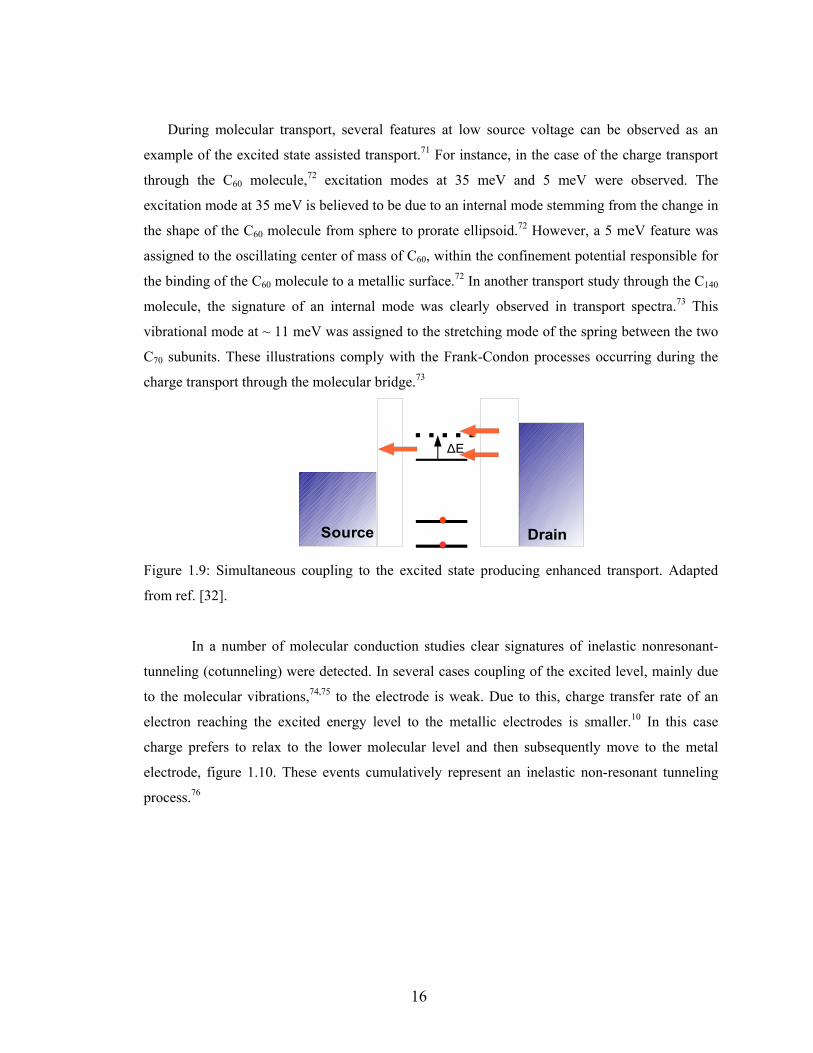
16
During molecular transport, several features at low source voltage can be observed as an
example of the excited state assisted transport.71 For instance, in the case of the charge transport
through the C60 molecule,72 excitation modes at 35 meV and 5 meV were observed. The
excitation mode at 35 meV is believed to be due to an internal mode stemming from the change in
the shape of the C60 molecule from sphere to prorate ellipsoid.72 However, a 5 meV feature was
assigned to the oscillating center of mass of C60, within the confinement potential responsible for
the binding of the C60 molecule to a metallic surface.72 In another transport study through the C140
molecule, the signature of an internal mode was clearly observed in transport spectra.73 This
vibrational mode at ~ 11 meV was assigned to the stretching mode of the spring between the two
C70 subunits. These illustrations comply with the Frank-Condon processes occurring during the
charge transport through the molecular bridge.73
ΔE
Drain Source
Figure 1.9: Simultaneous coupling to the excited state producing enhanced transport. Adapted
from ref. [32].
In a number of molecular conduction studies clear signatures of inelastic nonresonant-
tunneling (cotunneling) were detected. In several cases coupling of the excited level, mainly due
to the molecular vibrations,74,75 to the electrode is weak. Due to this, charge transfer rate of an
electron reaching the excited energy level to the metallic electrodes is smaller.10 In this case
charge prefers to relax to the lower molecular level and then subsequently move to the metal
electrode, figure 1.10. These events cumulatively represent an inelastic non-resonant tunneling
process.76
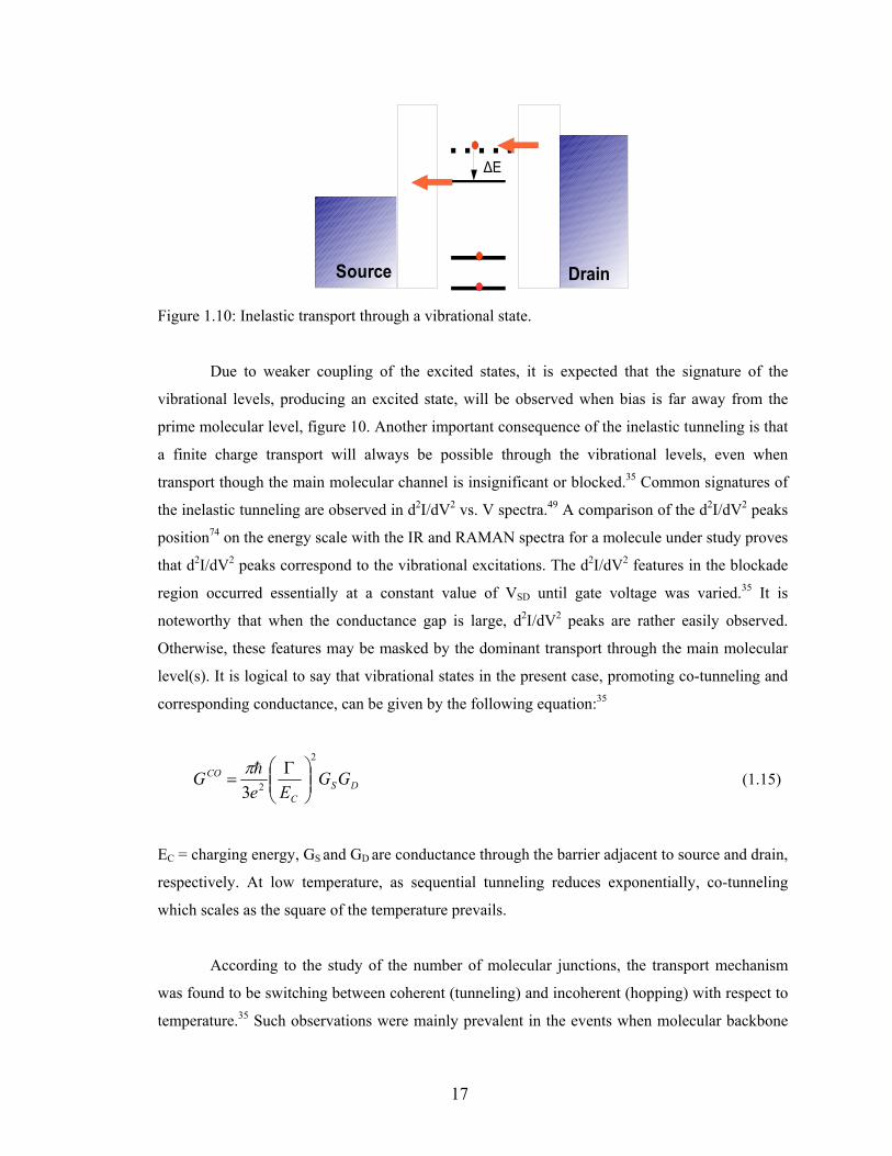
17
ΔE
Drain Source
Figure 1.10: Inelastic transport through a vibrational state.
Due to weaker coupling of the excited states, it is expected that the signature of the
vibrational levels, producing an excited state, will be observed when bias is far away from the
prime molecular level, figure 10. Another important consequence of the inelastic tunneling is that
a finite charge transport will always be possible through the vibrational levels, even when
transport though the main molecular channel is insignificant or blocked.35 Common signatures of
the inelastic tunneling are observed in d2I/dV2 vs. V spectra.49 A comparison of the d2I/dV2 peaks
position74 on the energy scale with the IR and RAMAN spectra for a molecule under study proves
that d2I/dV2 peaks correspond to the vibrational excitations. The d2I/dV2 features in the blockade
region occurred essentially at a constant value of VSD until gate voltage was varied.35 It is
noteworthy that when the conductance gap is large, d2I/dV2 peaks are rather easily observed.
Otherwise, these features may be masked by the dominant transport through the main molecular
level(s). It is logical to say that vibrational states in the present case, promoting co-tunneling and
corresponding conductance, can be given by the following equation:35
DSC
CO GGEe
G2
23 ⎟⎟⎠
⎞⎜⎜⎝
⎛ Γ=
hπ (1.15)
EC = charging energy, GS and GD are conductance through the barrier adjacent to source and drain,
respectively. At low temperature, as sequential tunneling reduces exponentially, co-tunneling
which scales as the square of the temperature prevails.
According to the study of the number of molecular junctions, the transport mechanism
was found to be switching between coherent (tunneling) and incoherent (hopping) with respect to
temperature.35 Such observations were mainly prevalent in the events when molecular backbone

18
possessed a functional group with the rotational freedom.60 Rotation of the functional group, a
thermally activated process, significantly changes the electronic coupling between the two nearest
molecular segments. A decrease in electronic coupling increases the molecular barrier height and
coherent tunneling mechanism prevails. However, larger electronic coupling decreases the
molecular barrier height, leading to the hopping type mechanism. As an example, a single
molecule of oligothiophene, possessing a rotatable NO2 group, is worth considering,60 figure
1.11(a). This molecule exhibited a thermally activated transport mechanism up to 100 K; below
this temperature coherent tunneling prevailed, figure 1.11(b). A similar study of the
oligophenylene molecules grafted on a glassy carbon substrate McCreery group obtained the
thermal signature of the change in the transport mechanism.10
HS
(a)
SH
NO2
-28
-21
-14
0.00 0.03 0.06 0.09 0.12
1/ T (1 / K)
ln (
I )
1V
0.2V
0.1V
(b)
Figure 1.11: Molecule backbone with a functional group with rotational freedom (a) experience
change transport mechanism with temperature (b). For higher bias, transition point between two
mechanisms is smearing out. Adapted from ref. [57].
The above mentioned case is possible when a tunneling electron strongly interacted with
the molecular environment, leading to decreased coherence and mechanism switching to
thermally activated transport.10 Such interaction mainly depends on the interaction time, for the

19
duration of which an electron remains in the molecular environment. The conduction time,
according to Landaur -Buttiker treatment,77 can be given by τ = Nh/2πΔE, where ΔE is the energy
gap between the Fermi energy level and active molecular orbitals, N = no. of molecular
subunits.10,64 A longer time for the electron to stay on the molecule promotes mixing up of
vibration with the transfer matrix elements, governing the transport.10 It is noteworthy that for the
shorter molecule, with a large energy barrier and a smaller barrier height, tunneling rate is fast.
However, for a long molecule with multiple subunits, barrier height is relatively small and
hopping is the dominant charge transport mechanism.
1.2 Spin-valves and role of the spin in the molecular transport:
The primary interest of incorporating the spin in the molecular electronic devices is to
form a molecular spin valve.16 Since most of the molecules exhibit non linear transport
characteristics, if one connects them with two ferromagnetic electrodes, the whole device will be
equivalent to a magnetic tunnel junction (MTJ) device.78 A MTJ structure possesses two
ferromagnetic (FM) electrodes separated by nm thick insulating spacer, figure 1.12.78
Figure 1.12: Typical stack of a magnetic tunnel junction.
The performance of a spin valve is mainly described in terms of the tunneling magneto
resistance ratio (TMR),79 a function of resistance values of spin valves in parallel (Rp) and
antiparallel (Rap) states of the two magnetic electrodes.78
100..1
..2100.)(
21
21
PPPP
RapRpRapTMR
+=
−= (1.16)

20
P1 and P2 are the degree of spin polarization80 of the first and second electrode, respectively. It is
instructive to consider the Rp and Rap in terms of the DOS81 of up (D↑) and down (D↓) spin of the
FM electrode, according to the following expressions.
)/(1 22↓↑ +∝ DDRp (1.17)
)..2/(1 ↓↑∝ DDRap (1.18)
TMR originates from the difference in the density of states (DOS) of the spin up D↑(EF)
and the DOS for the spin down D↓(EF) near Fermi energy (EF) level.18,81 To abide with the
conservation of spin orientation during tunneling, electrons are only permitted to move between
the subbands of the similar spin orientation, as depicted in figure 1.13. The magnetization of
electrodes controls the DOS of spin in subbands; tunneling rate for a specific spin is proportional
to the product of the DOS of this spin in the respective spin subbands of the two FM electrodes at
EF.

21
Figure 1.13: Transport between spin subbands of the two ferromagnetic electrodes in the parallel
(a) and antiparallel state (b). Thick line (thin dashed line) shows the high (low) spin current.
Adapted from ref. [23].
How a MTJ works as a spin valve can be described in the following manner. For a typical
~2nm thick insulator, two FM electrodes are antiferromagnetically coupled via insulator, e.g
alumina and exhibit high resistance state (Rap).17 Application of the magnetic field, strong
enough to overcome the antiferromagnetic coupling between the two electrodes, aligns the
magnetization of the two electrodes parallel to each other and hence produces smaller device
resistance, (Rp). An example82 of a TMR ratio for the MTJ with CoFe/Al2O3/NiFe configuration
is given in figure 1.14. It is noteworthy that the TMR peak is slightly shifted from the zero point
on field scale; it is attributed to the stray field arising from the MTJ stack itself producing a non

22
zero field even in the absence of an external field.83 In a more popular scheme, the magnetization
direction of one FM electrode is pinned and magnetization of the other electrode is freely
switched with magnetic field. In the later case, the least exchange coupling energy is desirable to
do switching with a smaller magnetic field. To flip the spin orientation of two ferromagnetic
layers, it is quite reasonable to assume that the amount of energy produced by the corresponding
magnetic field should be more than the exchange coupling energy. On energy scale, 1Tesla
magnetic field is equal to ~1K temperature. A smaller switching field (> ~100Gauss) is aimed to
produce integrable spin devices.
-150 -100 -50 0 50 100 1500
2
4
6
8
10
12
14
16
18
Field(Oe)
TMR
(%)
Figure: 1.14 Percent tunneling magneto resistances versus applied field curve for the
CoFe/AlOx/NiFe MTJ. Adapted from ref. [79].
The degree of spin polarization of the FM electrode significantly affects the TMR of a
MTJ.18 According to Julliere78, considering that spin polarization is a material constant, TMR
should always be less than 50%. This is close to the best TMR obtained with an alumina
insulating barrier.17 Attempts to use 100% spin polarized to increase TMR did not yield
significant change.17 The reason is mainly due to the strong interface associated with spin
scattering, precluding the transfer of 100% spin polarized current from one electrode to another17.
Another plausible reason may be that the band structure of a spin polarized material at interface is
significantly different from the bulk material.83

23
Replacing an alumina barrier with magnesium oxide (MgO) yielded as high as 250%
TMR.18 This study suggests that spin-polarization near FM-insulator interface is not a material
constant;18 spin polarization can be significantly different from the bulk. Tsymbal and coworkers
have theoretically shown that the spin polarization of ferromagnetic metal changed due to the
absorption of oxygen atoms on the surface of a ferromagnetic metal.84 Moreover, in the case of
the gold nanoparticles, the evolution of ferromagnetism was found to be the direct corollary of
change in surface chemistry using thiol terminated alkanes.85 These observations open doors for
the manipulation of spin polarization through the change in surface chemistry and then applying
them for the spin valve fabrications.
Major hurdles in the advancement of MTJ development are specific to material. Insulator
and FM-insulator interface roughness significantly contribute to the spin flip events precluding
the realization of the full potential of a MTJ device. Irregular insulator thickness between two FM
electrodes produces orange peel effect, disabling the independent switching of ferromagnetic
layer.17 Another tantalizing issue is to produce the same thickness and quality of ultrathin
insulator17.
Organic molecules are highly competent to replace inorganic insulators.26 Organic
molecules are known to exhibit long spin coherence length due a relatively small spin-orbit
coupling and hyperfine splitting.26 Organic molecules also possess fixed length and readily make
well defined chemical bonds with the metal surface once functionalized appositely. Molecules are
supposed to attach to the ferromagnetic electrodes through self assembly chemistry, which in turn
may also affect the degree of spin polarization of FM near interface,84 at least, to yield higher
effect on TMR than expected. Recent theoretical work showed the possibility of achieving
~600% TMR with 1, 4 tricene-dithiolate molecules between Ni contacts, and rekindled the
interest in molecular Spintronics.19 In a little more radical prediction, Petrov et al. quoted that “In
the case of antiferromagnetically ordered molecular wires, the inter electrode tunnel current may
be changed up to 7-8 orders of magnitude if a magnetic field has been applied”.30 In addition, a
low dimensional electronic system with molecular magnets, akin to single molecular magnets
with insulating alkane tethers, etc. was considered promising to realize their prediction.14
Petta et al.16 have prepared a nickel-octane thiol-nickel spin valve in a nanopore
geometry. These molecular spin valves were reported to exhibit as high as ~17% magneto
resistance ratio at 4.2 K. Because the octane-thiol molecule behaved as a tunnel barrier between
two ferromagnetic electrodes, the overall device is one form of the tunneling magneto resistance
(TMR) devices and is expected to follow the mechanism of conventional MTJ.18 However, large
scatter in transport data, the need of cryogenic temperature, and insufficiently characterized metal

24
molecule interfaces are suggestive of the long way ahead for making molecular spin valves,
which can at least compete with conventional MTJ spin valves.25 Pasupati et al. have prepared a
molecular spin valve by inserting a C60 molecule between the nm gap of Ni breakjunction.13 This
study reports ~17% TMR but more interesting is the observation of Kondo splitting. We discuss
the Kondo level splitting observation elsewhere in this review. Break junctions are highly
irreproducible and poorly characterized.86 Due to a low yield complex fabrication scheme, break
junctions are apparently unsuitable for the molecular spin valve structures.
The dearth of sufficient successful experimental attempts to form molecular spin devices
has not given requisite boost to the much vaunted field of molecular Spintronics.20 However, a
number of magnificent observations have surfaced due to the role of the spin state of molecules in
the molecular transport. The Kondo effect,31 complete charge suspension, negative differential
conductance,33 Zeman splitting,39 and exchange interaction produced an extremely high exchange
field.13 The impressive experimental observation strongly indicates that studying the role of spin
in molecular transport with a variety of electrodes which can reveal a treasure of new scientific
phenomenon.
The C6013 molecules and divanadium complexes,39 physiosorbed on the gold electrodes of
a break junction, have shown the Kondo phenomenon. The Kondo effect in molecular junctions
is a coherent many-body state,87,88 which evolves due to the antiferromagnetic exchange between
the localized spin of the molecule and the spins of the conduction electrons of the lead. Kondo
resonance89 brings about an enhanced density of the states at the metal electrode that leads to the
zero bias conductance peaks.
A molecule generally acquires a net spin after being connected to two model electrodes
through tunneling barriers. When these tunneling barriers are reasonably transparent, the wave
function of the unpaired electron at the molecular level can leak out through barriers to hybridize
with the delocalized electrons in the contact. If the hybridization step makes the spatial wave
functions of the localized electron on a molecular level and delocalized electrons at the metal
electrode symmetric, then the spin part of the wave functions for the electron at the molecule. The
interacting electron of the electrode has to be the anti-parallel of the antiferromagnetically
coupled. According to the Pauli rule,47 the overall wave function of the interacting fermions have
to be antisymmetric. The coupling energy of interacting electrons at the molecule and at the lead
can be defined in terms of a characteristic temperature, popularly known as Kondo temperature
(TKondo).39

25
2)/.exp( Γ−Γ
=επC
Kondo
ET (1.19)
Ec = charging energy
ε = difference between localized state and the Fermi level
Γ = summation of coupling strengths of energy level with two electrodes, ΓS and ΓD are the
coupling strength of energy level with source and drain respectively.
The Kondo state is stable for ε/Γ >> 1. It is noteworthy that non-uniform source-drain
coupling can bring about a higher Kondo temperature39. Interestingly, Kondo resonance in bulk
metals due to dilute magnetic impurities enhances scattering events for conduction electrons.
Scattering due to the antiferromagnetic interaction between the localized spin of impurity and
delocalized spins of conduction electrons increases resistivity.90
Liang et al.39 have studied the Kondo resonance with the divanadium molecular complex.
The choice of the divanadium molecule was based on the control of its spin degree of freedom in
a predictable manner. As high as 30 K Kondo temperature was realized. Interestingly, the
application of a magnetic field was found to produce a 230 µV/T splitting in Kondo resonance
level.39 This splitting magnitude of Kondo level was consistent with the Zeeman splitting
calculated by 2gµB B/e, where g=2 is the g factor for the molecule, and µB is the Bohr magnetron.
It was also observed that the vanadium complex possessed a V2+ ion state, producing a spin
doublet (s = ½) state between the two electrodes. It is noteworthy that the V2+ ion state was not
realized in the bulk state.39
Numerous studies showing Kondo resonance39 have been reported with the physio-sorbed
molecule(s) in the gap of the break junction electrode. Here metal molecule contacts are far from
being robust90. Netlson and coworkers have encountered the irreversible switching from Kondo
resonance mode to Coulomb blockade90. This change can be associated with the change in the
physical coupling between the metal and the molecule; this event hints towards the instability of
the metal-molecule bond.
A plausible way to tackle the instability of the metal-molecule contact is to use molecules
with organic tethers ending with a metal affinitive functional group.33 Using alkane molecules is
apparently a good choice over the conjugated tethers91. A π bond misalignment, producing a high
resistive state, may mask the true properties of the core molecule23. Bond tunneling via alkane
tethers, even though they exhibit insulating attributes, is much more efficient than the tunneling

26
through space. Another clear advantage is that metal molecule coupling can be easily tailored to
be weak to strong by changing the length of the alkane tethers.
Park et al.31 have given an excellent demonstration of imparting a control on the
molecular transport mechanism by controlling the metal molecule coupling with the help of
alkane tethers of different lengths. It is noteworthy that metal molecule coupling is exponentially
dependent on metal molecule separation. It was found that changing the tether lengths attached to
a cobalt coordination complex changed the transport mechanism from the single electron
transistor regime to the Kondo regime. It has also been observed that alkane tethers work as a
guiding channel for electron transport so that it tunnels to the molecule core, interacts with it, and
then tunnels to the other electrode via another tether. For the longer molecule, molecular devices
showed a strongly suppressed transport to a threshold voltage, which depended on the gate
voltage. Beyond the threshold voltage, the current increased in step. This transport characteristic
is of a single electron transistor device. For a larger gate voltage, cobalt with a paired electron and
with s = 0 spin state resulted. However for a smaller negative gate voltage, cobalt with an
unpaired electron and with s = ½ spin state was active. In the latter case i.e., a higher spin state
current through the molecule would be suspended by a Clebsh-Gordan coefficient.
The smaller molecular [Co(tpy-SH)2] was shown to exhibit a Kondo resonance at zero
bias31. Since a smaller molecule metal gap produces a stronger wave function delocalization
through barriers, the existence of a high exchange coupling between molecular spin state and
electrode spin become viable. The application of the magnetic field was found to split the Kondo
resonance peak. This is expected due to the Krammer degenerate Co2+ charge state (3d7) with an
unpaired electron that splits in the magnetic field. Another possible charge state, i.e., Co3+ (3d6)
has paired electrons and s = 0 spin state, will not undergo Zeeman splitting31.
In the aforementioned cases, Kondo resonance was observed when a molecule with a low
spin state (s = ½)31 interacted with the nonmagnetic gold electrode. Typical level splitting under
the effect of the magnetic field was ~200 µV/T31, which is consistent with the typical Zeeman
splitting.
A striking observation of Kondo resonance and its splitting was observed when a C60
molecule was placed between the two ferromagnetic electrodes of a Ni break junction.13
Interestingly, the experimental realization shown here13 was found to be in close agreement with
the prediction of Kondo level splitting, even in the absence of a magnetic field for the system of a
quantum dot coupled to magnetic electrodes.92 In this study,13 the shape of the two electrodes
were designed to give them different shapes in order to induce magnetic anisotropies, figure
1.15(a). Different magnetic anisotropies allowed the magnetic reversal of the two electrodes at

27
dissimilar magnetic fields. Kondo resonance is generally suppressed by ferromagnetic ordering;88
hence, it is rather surprising to see the existence of the Kondo resonance peaks in the present
case.13 Even more intriguing is the observation of as much as 16 meV Kondo level splitting,
which is likely to occur under the application of a ~70 T field,13 figure 1.15(b). Such a large
splitting can not be due to the Zeeman splitting of the Kondo level in the external field.56. The
Zeeman splitting observed on a junction comprising a C60 molecule and gold break junction was
found to be ~230µV/T, 39 figure 1.16.
-60 -40 -20 0 20 40 600.00
0.03
0.06
0.09
0.12
0.15
0.18
V (mV)
Con
duct
ance
(e^2
/h)
Ni-C60-Ni
(b)
Figure 1.15: Schematic of Ni break junction with C60
1 molecule (a). Splitting of Kondo
resonance level by ~16mV due to the effect of exchange induced high magnetic field on C60
molecular level. Adapted from ref [10].
The extent of the splitting was found to be tunable by the application of an external
magnetic field, aiming to set the magnetization of the two electrodes parallel and anti-parallel
with respect to each other. For the parallel (anti-parallel) orientation of electrodes, Kondo level
splitting was found to be 16 meV (7.5 meV)13.
In the present case, it is apparent that the two many-body-correlated states88,93 are in
competition. First, correlated state occurs due to the coupling between the localized spin of the
molecule and the itinerant spins of the electrode(s); the second correlated state is associated with
the itinerant electron ferromagnetism of the electrodes.88 A strong coupling between the molecule
and metal electrode, presumably via electron transparent barriers, creates a strong magnetic
exchange coupling.93 Due to the spin polarization of electrodes and a strong exchange coupling of
28
molecular levels with metallic states, an exchange field arises which contributes to the Zeeman
splitting.39 In this case modified expression for the Zeeman splitting is following:13,92
∑ Γ+=Δ = mmLRmB PaBgVe ,.2 μ (1.20)
It is believed that due to quantum charge fluctuations, the spin asymmetry in the coupling
of the molecular level to the ferromagnetic electrodes, produces a spin dependent renormalization
of the molecule’s level in the proximity of the Fermi level.13,92 The spin dependent
renormalization breaks the spin degeneracy for the spin up and spin down states to bring about a
splitting of the conductance curve, as expected from an external magnetic field.92 It is important
to note that if ΓL = ΓR, then for the anti-parallel magnetization of leads the effects of exchange
interactions of molecular level with the two electrodes will cancel each other.56 Kondo resonance
will occur without splitting.13 It can be inferred that the utilization of magnetic leads with
dissimilar magnetization attributes will produce Kondo splitting rather easily.
-4 -3 -2 -1 0 1 2 3 40.20
0.25
0.30
0.35
0.40
0.45
0.50
H = 0In magnetic field
V (mV)
Con
duct
ance
(e2/
h)
Au-C60-Au
Figure 1.16: Kondo resonance peak for the C60 molecule between the two electrodes of gold
break junction. Kondo resonance peak undergo Zeeman splitting when external magnetic field
(H) is applied. Adapted from ref. [10].
29
We observed how a C60 molecule mediated to produce extremely strong exchange
coupling between the two Ferromagnetic electrodes. In a relevant theoretical study it was found
that impurities, considering them analogous to molecule, within the tunnel barrier of a magnetic
tunnel junction can enhanced exchange coupling94 by ~3 orders in magnitude.95 It was calculated
that an impurity level close to the Fermi energy level and physically present at the center of the
tunnel barrier were highly influential, figure 1.17(a), in increasing the inter-electrode exchange
coupling, figure 1.17(b). Strength of impurity assisted exchange coupling was shown to directly
depending upon their concentration.
EI =0.2 eV
EI =-0.2 eV
EI =0 eV
FM1 FM2
(a)
4 5 6 7 8 9 10 11-1
-0.8
-0.6
-0.4
-0.2
0
0.2
Ei = 0.0 eV E=-0.2 eVEi = 0.2 eV
Dinstance ( Å )
J ( e
rg /
cm2
)
(b)
Figure 1.17: Band diagram of a MTJ showing the position of the impurity levels within the tunnel
barrier (a) enhancing the exchange coupling energy between two FM electrodes. Exchange
energy versus impurity position in tunnel barrier for the three energy levels with respect to Fermi
energy level. Exchange coupling energy via impurity free barrier is ~1x10⁻³ erg/cm2. Adapted
from ref. [92].
It is evident that molecule or strongly coupled quantum dots to the ferromagnetic
electrodes96 can produce an extraordinarily strong exchange field,56 which is not attainable within
a laboratory. This magnetic field, around the junction, has been experimentally seen to influence
the molecular levels.13 Can the same strong exchange field97 also affect the band structure of the
ferromagnetic metals by producing Zeeman like splitting? If so then band offset for the spin up
and spin down DOS is going to be more than the Stoner splitting.46 Zeeman splitting for an
electron level and the shift in Fermi level of a ferromagnetic metal (ΔH), due the application of
magnetic field H, are ±0.5(gµ0µBH) and ±0.5(Pgµ0µBH), respectively46.

30
A direct consequence of the larger band offset will be the larger difference in the spin
populations of a ferromagnetic metal (FM), figure 1.18. In the conductance versus magnetic field
study of ferromagnet-quantum dot-ferromagnet system observed conductance fluctuations were
attributed to the Zeeman splitting of ferromagnetic metals.98 This study insinuates that the
molecule induced strong exchange field between two FMs has the potential to dramatically affect
the molecular junction transport. Moreover, recent theoretical study on the strongly coupled
quantum dot to the magnetic electrode considered various forms of the band diagrams of the
ferromagnetic metals to capture the precise physics of strongly coupled ferromagnetic electrode
system.99
Since atom(s) of the FM metal experiencing the molecule/quantum dot mediated field are
also coupled to the atoms of the bulk via Heisenberg exchange coupling,99 localized effect can
give rise to a long range magnetic ordering. However, the experimental study of the change in the
magnetic properties of the ferromagnetic electrode(s) due to molecules, quantum dots and
impurity would need sample size much bigger than the brekjunctions.13

31
ΔΔ
EF(0)
EF(H)
ΔH
EF(H)=Fermi Energy in H magnetic field
EF(0)= Fermi energy in zero magnetic field
Δ= Stoner splitting ΔH= Zeeman splitting energy
Figure 1.18: External magnetic field producing redistribution of spin density and shift in Fermi
energy level of in ferromagnetic band. Adapted from ref. [53].
By now we have seen the effect of molecular spin state on the molecular transport in
mainly s = ½ or low spin states. Utilization of the high spin state molecules33 such as single
molecular magnets (SMM) in molecular junction can be very interesting; SMMs are promising
candidates for producing molecular spin devices which are switchable due to light and magnetic
field.8 Heersche et al.33 produced gold break junction based molecular junction by bridging
[Mn12O12(O2C-R-SAc)(H2O)4] molecules, described as Mn12. Here R refers to alkane tethers. It
helps SMM binding to metal electrodes, separated by a nanogap, to create robust bond, which
also serves as tunnel barrier. It was reported that a SMM based molecular junction exhibited
negative differential conductance (NDC) and total charge current suppression phenomenon.
Interestingly, a single SMM based molecular junction was reported to show three different charge
transport regions in the conductance-bias voltage-gate voltage spectra. “This kind of behavior is

32
otherwise expected to arise from three different quantum dots”.33 This result hints towards the
possibility of using same molecular junction for the different device characteristics. These
different charge transport regions were assumed to be associated with there different states of the
same molecule.
Authors have summarized that CCS and NDC in SMM molecular junction is due to the
intrinsic characteristic of molecules. For the quantitative explanation of experimental results a
sequential tunneling model with spin Hamiltonian of SMM has been considered. The spin
Hamiltonian is believed to capture the effect of the high spin ground state of SMM and its ladder
of spin excited states in transport of SMM junction.33 From the analysis it is apparent that a
sequence of tunnel processes can yield a non-equilibrium population of certain excited states.
Subsequent depopulation from these excited states will occur slowly by violating the spin
selection rule, due to quantum tunneling of magnetization.29 In this event transport of charge was
shown to be hampered to produce CCS and NDC observations. In a theoretical study of a system
of SMM attached to two ferromagnetic electrodes, it was calculated that interference between
different tunneling paths within the molecule can produce a dramatic current suppression.
Interference between molecular states lead to Berry phase.32 With the aim of studying SMM
based molecular junctions in magnetic field thoroughly, similar SMM functionalized100 and
unfunctionalized39 has been utilized. The device instabilities, potential damage to SMM,
irreproachability appear to plague the further progress.101 Moreover, STM study, in which it is
quite easy to controllably address single SMM, could reveal that the SMM has ~1.0 V HUMO –
LUMO gap.102
From the above given discussion it is clear that molecule based spin devices are
promising for the making of spin-valve devices. Utilizing molecular bridges between two metallic
electrodes allows exploring of new spin dependent phenomenon in metal-molecule systems. A
more interesting, yet challenging idea is to attach high spin state molecular complex3 to
ferromagnetic leads to produce molecular spin valves.40 Advancement of molecular spin device
would ultimately rely on their functioning at room temperature. For this devices do not have to be
based on single molecule.
33
1.3. Molecular electrode design for molecular spintronics:
Fabrication of molecular spintronics devices13 is expected to be more challenging than
that for molecular electronics devices and magnetic tunnel junctions18. Producing reproducible
molecular device with ferromagnetic electrodes, functioning at RT, is a daunting task. On the
other hand fabrication of a MTJ with a metal oxide insulator that possesses the virtue of
molecules (long spin coherence, reproducible fixed length to atomic dimensions and well defined
metal/molecule interface) is apparently implausible. A practical molecular spin device is expected
to unite attributes of a MTJ17 and molecular devices4.
What can be the suitable device design for molecular spin devices can justified from the
following discussion. In one of the pioneering experimental attempt Petta et al.16 have fabricated
molecular magnetic tunnel junction with nanopore geometry. These devices mainly studied at
cryogenic temperatures and exhibited large device to device scatter. In order to make the top
metal contact with active molecules, physical vapor deposition was performed on the monolayer
self-assembled on metallic surface. This scheme is inevitably likely to suffer with the impurities
coming arising due to diffused metal atoms and self assembly step34. Since device lateral
dimensions are very small due to nanopore geometry adverse effects of the impurity and defects
could be minimized; as high as 17% TMR could be observed at cryogenic temperature16.
Moreover, metal deposition steps for nanopore geometry are quite tricky. Such schemes are
unlikely to yield reproducible molecular spin devices purely dictated by the attributes of
molecules.
Break junctions have been the most popular test pads for studying the influence of
molecular magnetic state on molecular transport.13 Break junctions are rather easy to produce
with gold electrodes and have been employed to observe Kondo effect, a magnetic correlated
state.86 In our knowledge only in one study break junction with Ni magnetic electrodes were
successfully employed. Break junctions based devices are excellent test pads but suffer with poor
reproducibility and very low yield.86 Every break junction device has dissimilar environment for a
molecule. Atomic defects in break junction can also imitate the attribute of a molecule.86. For
instance a celebrated Kondo effect due to molecules could be seen in bare break junctions;103
difficulty in studying break junctions before molecule attachment can make any finding
questionable.90 The two metal electrodes of a break junction are of same; molecular spin devices
can not use highly refined multilayer configuration of top and bottom electrodes utilized in
magnetic tunnel junctions.
34
Magnetic tunnel junctions having the possibility of attaching molecules between two
metallic electrodes similar to the break junction device can be the basis of successful molecular
spin devices. By default magnetic tunnel junction utilizes molecular dimension metal oxide
insulators. An ion milled MTJ stack, with sharp vertical cut, reveals the sharp edges where
looking from the side one finds that the top and the bottom electrode possesses the open site for
the bridging of molecules between two metal electrodes. This minimum distance between the two
electrodes is equal to the insulator film thickness. Since in a typical MTJ lateral dimensions are of
few microns to hundreds of nm large, a big population of molecules will have the opportunity to
form molecular junction. The large number of molecular channels is expected to dictate the
molecular transport. One can imagine this design is akin to break junction. One can consider that
break junctions are made perpendicular to the plane of substrate and kept abut to form a parallel
array of break junctions. Aim of following work is to realize a tunnel junction based molecular
spin device.
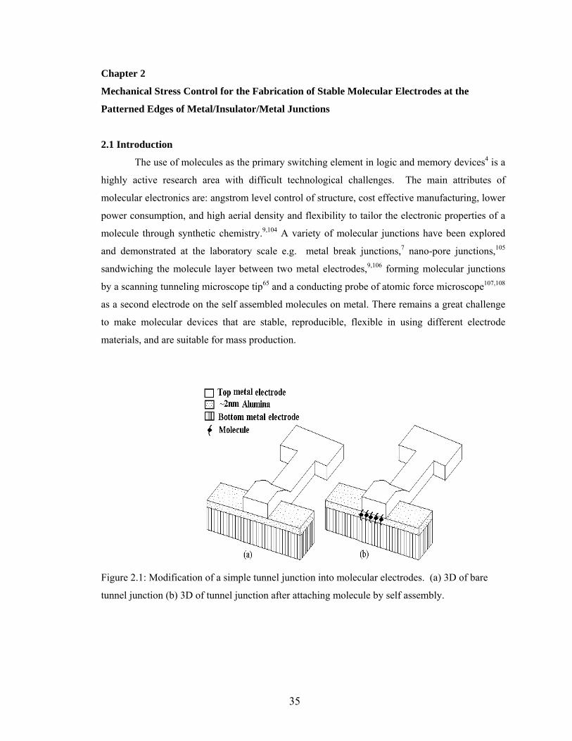
35
Chapter 2
Mechanical Stress Control for the Fabrication of Stable Molecular Electrodes at the
Patterned Edges of Metal/Insulator/Metal Junctions
2.1 Introduction
The use of molecules as the primary switching element in logic and memory devices4 is a
highly active research area with difficult technological challenges. The main attributes of
molecular electronics are: angstrom level control of structure, cost effective manufacturing, lower
power consumption, and high aerial density and flexibility to tailor the electronic properties of a
molecule through synthetic chemistry.9,104 A variety of molecular junctions have been explored
and demonstrated at the laboratory scale e.g. metal break junctions,7 nano-pore junctions,105
sandwiching the molecule layer between two metal electrodes,9,106 forming molecular junctions
by a scanning tunneling microscope tip65 and a conducting probe of atomic force microscope107,108
as a second electrode on the self assembled molecules on metal. There remains a great challenge
to make molecular devices that are stable, reproducible, flexible in using different electrode
materials, and are suitable for mass production.
Figure 2.1: Modification of a simple tunnel junction into molecular electrodes. (a) 3D of bare
tunnel junction (b) 3D of tunnel junction after attaching molecule by self assembly.

36
Recently, a new class of molecular electrodes109,110 has been reported where thin film
thickness is utilized to set the nm-scale gap between two electrodes. A key advantage of this
approach is that metallic contacts with a wide variety of metals,9 including ferromagnetics for
molecular spin-injection, can be incorporated into the design. One way to make stable molecular
electrodes with a large difference between background current (in planar area of electrode) and
molecular current (at the edge of the pattern) is to use a thick insulator (4-10nm) and then attach
long molecular chains to bridge the insulator gap.111 Ideally, the separation between two metal
electrodes can be set to the dimensions of single molecular clusters offering well-defined
molecular conduction paths as schematically shown in figure 2.1. As a practical consideration,
the background tunnel current is too high for junctions <~1nm for small molecule conduction,
hence the larger molecular dimensions of clusters (~2nm) are favored in this geometry. However,
the major challenge even at 2nm thickness is to produce a stable insulator barrier with low
leakage current through the planar junction area thus allowing molecular conduction paths at the
pattern edge to dominate. Depending upon molecule design, conduction through the molecule can
be controlled by the external input such as light, magnetic field, and chemical environment. In
this chapter we illustrate the role of mechanical stresses on the tunnel barrier stabilityand
insulator deposition methods to counteract the effects of the stresses. Lastly we demonstrate
molecular electrode fabrication process.

37
2.2 Experimental details
Figure 2.2: (a) Metal-insulator-metal tunnel junction fabricated by sandwiching ~2nm Al2O3
between two metal electrodes. Bottom metal electrode (top metal electrode) is produced by
depositing 8nm Co and 2nmNiFe (only 10nm NiFe) in photolithographically defined pattern. (b)
Created window for ion milling to produce vertically sharp exposed side of tunnel junction, (c)
top view of tunnel junction after ion milling (f) optical micrograph from the top side of an actual
ion milled TJ (d) side view of sharp and exposed metal-insulator –metal TJ after ion milling (e)
ion milled TJ after molecule attachment or bridging the molecule across insulator gap. (g) 3D
AFM image of ionmilled TJ in the rectangular are a as shown in (f). Note width of top electrode
is 5µm. Bottom electrode dimension used in this study was ~2µm and ~8µm.
To understand the role of the stresses and their effects on tunnel barrier morphology of
metal-insulator-metal tunnel junctions utilized in our molecular junction scheme, unpatterned
samples without top metal and with metal-insulator configuration were prepared. The bilayers
possess a sufficient stress level to bring about similar morphological changes on the ultrathin
insulator, alumina in present work, as one would expect with metal-insulator-metal trilayers. This
approach made alumina directly accessible for the morphological study by the atomic force

38
microscope (AFM) and the transmission electron microscope (TEM). <100> Silicon (Si)
substrate with 100nm silicon oxide (SiO2) was utilized. For the TEM study, 50nm thick electron
transparent silicon nitride (Si3N4) windows on etched Si<100> was used as substrate. Throughout
this work, cobalt (Co) and nickel-iron (NiFe), with Ni:Fe::80:20 ratio, metals, and plasma
oxidized aluminum was utilized as an alumina (Al2O3) insulator. Unpatterned,
Si/SiO2(100nm)/Co(10nm)/Al2O3(~2nm) samples, were fabricated for the stress measurement
(using Veeco, Dektack 6M profilometer) and morphological study (using Digital Instrument
Multimode AFM) in contact mode. It was noted that the sputtering of the thin films inherently
produced compressive stresses in the samples and can be termed as a general case. However,
tensile stress was only observed after heating and mechanical bending of sample before
deposition in the sputtering instrument. The stress measurement was performed by the substrate
curvature method.112 Radius of curvature for the oxidized silicon substrate was obtained before
and periodically after the deposition of unpatterned Co(10nm) and then alumina(2nm) on it. The
substrate radius was then applied to the Stoney formula to calculate the nature and magnitude of
stresses. The Stoney formula connects the radius of curvature R, the in-plane component of the
stress σ0, and the thickness of both the bilayer structure (hl) and the substrate (hs), as given below
RhhE
l
ss2
0 )1(6 νσ
−= (2.1)
Where Es and ν are, respectively, the Young’s modulus and the Poisson’s ratio of the
substrate.Values of Es and νs for <100> silicon substrate are 130GPa and 0.2783 respectively.113
Wafer thickness (hs) is 400µm and total film thickness (hl) is 12nm.
A TEM study was also performed on an analogous system but with a different
composition. Titanium (Ti), for good adhesion, was placed between Co/Al2O3 bilayer and
electron transparent silicon nitride substrate present on the TEM grid to form
[Si3N4(50nm)/Ti(2nm)/Co(10nm)/Al2O3(2nm)] structure. For this study a 200 kV field emission
analytical transmission electron microscope (JEOL JEM-2010F) equipped with an Oxford
energy-dispersive X-ray spectrometer, a scanning (STEM) unit with a high-angle annular dark
field (HAADF) detector and a Gatan imaging filter (GIF) system was utilized.
Tunnel Junctions (TJ) [Si/SiO2(100nm)/Co(8nm)/NiFe(2nm)/Al2O3(2nm)/ NiFe(10nm)] for
molecular electrodes were prepared following the established magnetic tunnel junction
fabrication approach with 1-2 nm thick insulator layers as an active device element.18
Photolithography (using Karl –Suss mask aligner) for defining the pattern for multilayer
deposition, sputtering process (using AJA International Sputtering system) for depositing metal
electrodes and Al2O3 film, and ion milling (using FISCHIONE 1010 ion mill) for creating a sharp

39
exposed side edge of TJ, were utilized. NiFe is used on both sides of the Al2O3 due to its air and
chemical stability114 and better oxide coverage as compared to Au. From the TEM studies,115 it is
well established that the ion milling process reliably produces sharp vertical cuts on multilayer.
To avoid photoresist hardening, the sample was cooled by liquid nitrogen during ion milling.
Extra care was taken to avoid ion milling-caused damage to the thin Al2O3 barrier by adopting a
low angle and a low energy argon ion beam for milling. The molecular electrode fabrication
scheme is summarized in figure 2.2. Typical junction areas of a TJ were 10 and 40μm2 and the
effective length of the exposed edge, where molecules were attached, is 5μm.
Base pressure for sputtering was ~2x10⁻⁷torr for all the depositions. NiFe and Co films
were deposited using a RF-powered gun at 150W power and 1mtorr argon (Ar) pressure.
Alumina deposition, for molecular electrodes fabrication, was accomplished in two steps. In the
first (second) step 1nm (0.5nm) Al was deposited using a DC-powered gun with 75W power and
2 mtorr Ar pressure. Each Al deposition was followed by plasma oxidation for 30 seconds at
20W RF power and at 60 mtorr pressure of 1:1 argon and oxygen mixture. Details of alumina
deposition for stress and morphological studies are described elsewhere in this chapter. It is
noteworthy that sputtering parameters for NiFe, Co and Al deposition were individually
optimized to produce the least roughness value before the fabrication of molecular devices and
samples for the stress study.
Figure 2.3: Water contact angle was 11º on bare NiFe film(a) but increased to 58º after the
functionalization of NiFe metal with organometallic metallic molecules (b) used in this study.
A ~3nm long organometallic cluster (OMC) with thioacetate terminated tethers was
synthesized3 for the attachment across the insulator gap utilized in the present electrode design.
Through thiol surface attachment to metal leads, an array of OMC, [(pzTp)FeIII(CN)3]4[NiII(L)]4-
[O3SCF3]4 [(pzTp) = tetra(pyrazol-1-yl)borate; L = 1-S(acetyl)tris(pyrazolyl)decane], were
covalently linked to top and bottom electrodes to span the edge of the insulator film to form a
dominant conduction pathways.116 This molecule essentially comprises a cube of 8 edges of
cyanide bridged Ni and Fe atoms (-Ni-N≡C-Fe-). There are four 10 carbon alkane tethers
connected to Ni atoms of the molecule’s cube at one end and to the metal electrode, with thio-

40
acetate group, on another end.3 The thioacetate group is a protecting group to preclude thiol
reactions during the formation of an octametalic core. This thiolacetate group is readily removed
during an electrochemical molecule attachment process117 on the device to form thiol-Ni surface
bonds. To attach the molecule to electrodes, a 2mM solution of OMC in dichloromethane
(CH2Cl2) solvent was subjected to the alternating ±100mV biasing between two metal electrodes
with a time interval of 0.02 seconds for a period of 2 minutes. After the molecule attachment
process samples were rinsed with CH2Cl2, iso-propyl alcohol and DI water (18Mohm), the
samples were dried. Electrical properties of TJ before and after molecule attachment were
studied with Keithley 2430 1KW Pulse Source Meter. Effectiveness of the electrochemical step
in making metal-molecule bonds were confirmed by the contact angle measurement on the flat
NiFe metal film, used in the actual TJ to interact with molecules. It was found that the water
contact angle on NiFe film rose from 11(±1.5)º to 58(± 1.6)º after electrochemistry of molecules,
affirming the chemisorptions of the molecules on the metal films, figure 2.3. The reaction
between Ni metal and thiol ended molecules are well established. 118
2.3 Results and discussion
-400
-200
0
200
400
600
800
1000
Fresh 1 2 3 4
Time (Days)
Stre
ss (M
Pa)
Compressive stressTensile stress
Figure 2.4: Compressive and tensile stresses are relaxing with time on multilayer
Si/SiO2(100nm)/Co(10nm)/ Al2O3 (~2nm).
The thin alumina film insulator is the most important part of the Tunnel Junction (TJ)- based
molecular electrodes. The stability of a thin alumina film used in TJs has been nearly exclusively
characterized in terms of electrical breakdown voltage.119 Insignificant attention was given to the
role of mechanical stresses in the tunnel barrier breakdown. In our studies, we have observed that
both tensile and compressive stresses appeared in multilayer samples. First, we studied the stress
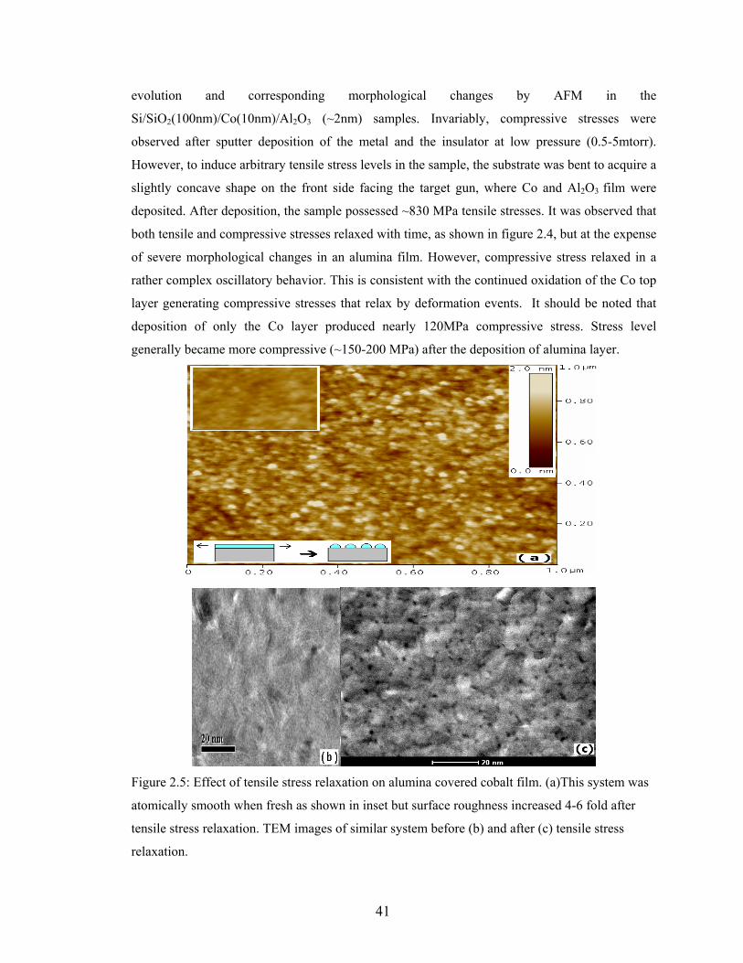
41
evolution and corresponding morphological changes by AFM in the
Si/SiO2(100nm)/Co(10nm)/Al2O3 (~2nm) samples. Invariably, compressive stresses were
observed after sputter deposition of the metal and the insulator at low pressure (0.5-5mtorr).
However, to induce arbitrary tensile stress levels in the sample, the substrate was bent to acquire a
slightly concave shape on the front side facing the target gun, where Co and Al2O3 film were
deposited. After deposition, the sample possessed ~830 MPa tensile stresses. It was observed that
both tensile and compressive stresses relaxed with time, as shown in figure 2.4, but at the expense
of severe morphological changes in an alumina film. However, compressive stress relaxed in a
rather complex oscillatory behavior. This is consistent with the continued oxidation of the Co top
layer generating compressive stresses that relax by deformation events. It should be noted that
deposition of only the Co layer produced nearly 120MPa compressive stress. Stress level
generally became more compressive (~150-200 MPa) after the deposition of alumina layer.
Figure 2.5: Effect of tensile stress relaxation on alumina covered cobalt film. (a)This system was
atomically smooth when fresh as shown in inset but surface roughness increased 4-6 fold after
tensile stress relaxation. TEM images of similar system before (b) and after (c) tensile stress
relaxation.
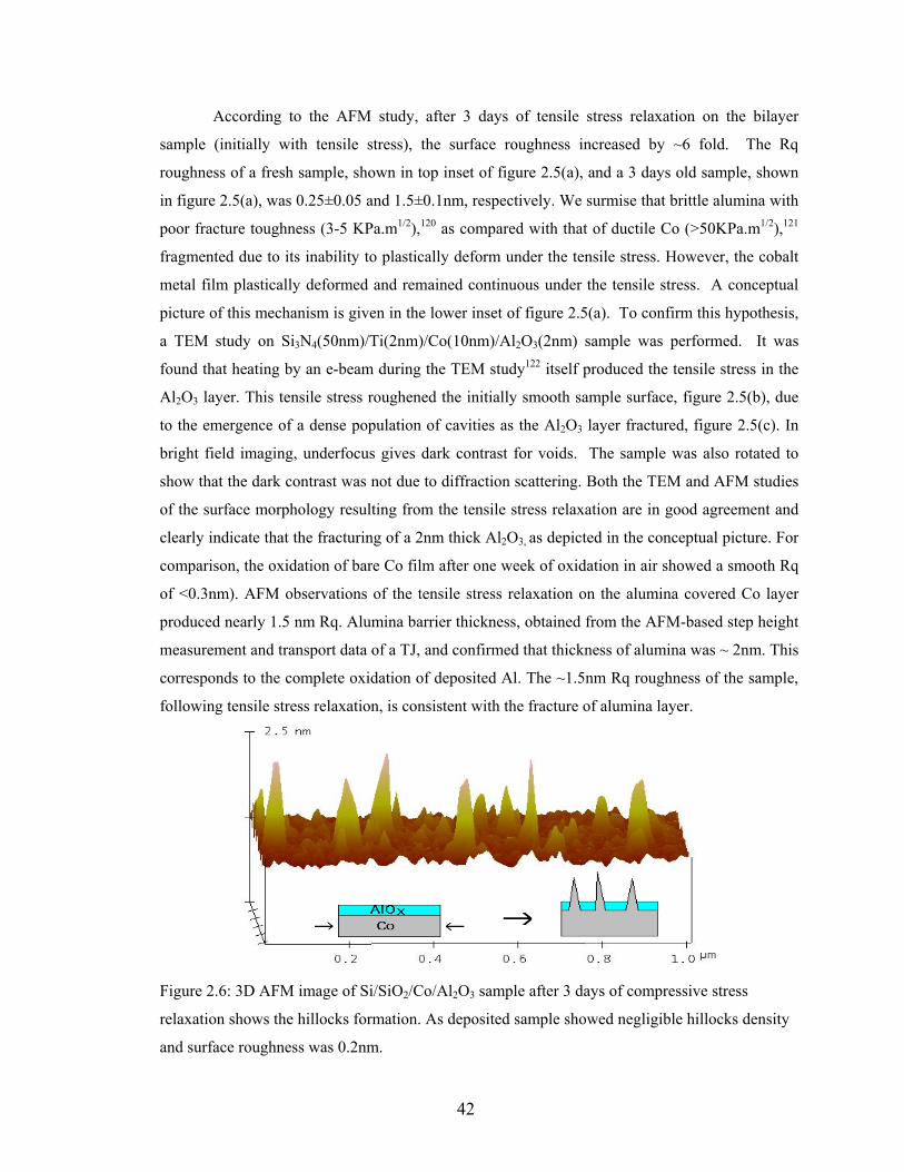
42
According to the AFM study, after 3 days of tensile stress relaxation on the bilayer
sample (initially with tensile stress), the surface roughness increased by ~6 fold. The Rq
roughness of a fresh sample, shown in top inset of figure 2.5(a), and a 3 days old sample, shown
in figure 2.5(a), was 0.25±0.05 and 1.5±0.1nm, respectively. We surmise that brittle alumina with
poor fracture toughness (3-5 KPa.m1/2),120 as compared with that of ductile Co (>50KPa.m1/2),121
fragmented due to its inability to plastically deform under the tensile stress. However, the cobalt
metal film plastically deformed and remained continuous under the tensile stress. A conceptual
picture of this mechanism is given in the lower inset of figure 2.5(a). To confirm this hypothesis,
a TEM study on Si3N4(50nm)/Ti(2nm)/Co(10nm)/Al2O3(2nm) sample was performed. It was
found that heating by an e-beam during the TEM study122 itself produced the tensile stress in the
Al2O3 layer. This tensile stress roughened the initially smooth sample surface, figure 2.5(b), due
to the emergence of a dense population of cavities as the Al2O3 layer fractured, figure 2.5(c). In
bright field imaging, underfocus gives dark contrast for voids. The sample was also rotated to
show that the dark contrast was not due to diffraction scattering. Both the TEM and AFM studies
of the surface morphology resulting from the tensile stress relaxation are in good agreement and
clearly indicate that the fracturing of a 2nm thick Al2O3, as depicted in the conceptual picture. For
comparison, the oxidation of bare Co film after one week of oxidation in air showed a smooth Rq
of <0.3nm). AFM observations of the tensile stress relaxation on the alumina covered Co layer
produced nearly 1.5 nm Rq. Alumina barrier thickness, obtained from the AFM-based step height
measurement and transport data of a TJ, and confirmed that thickness of alumina was ~ 2nm. This
corresponds to the complete oxidation of deposited Al. The ~1.5nm Rq roughness of the sample,
following tensile stress relaxation, is consistent with the fracture of alumina layer.
Figure 2.6: 3D AFM image of Si/SiO2/Co/Al2O3 sample after 3 days of compressive stress
relaxation shows the hillocks formation. As deposited sample showed negligible hillocks density
and surface roughness was 0.2nm.

43
Compressive stresses showed a different failure mechanism. The AFM study of the
Si/SiO2(100nm)/Co(10nm)/ Al2O3(~2nm) sample after 3 days of compressive stress relaxation
suggests the evolution of nano-hillocks or nano-coneslike features, figure 2.6. The typical
diameter and height of such features was 5-50nm and 0.5-5nm, respectively. We believe that
under the effect of compressive stress, hard alumina remains stable while the ductile Co metal
extrudes out through the weak points and pinholes in alumina film. A conceptual picture of the
related mechanism is shown in the inset of figure 2.6.
Figure 2.7: (a) TEM study show nano hillocks formation and their shadow on
Si/Ti(2nm)/Co/Al2O3/alumina multilayer. (b) Magnified version of nanohillock and (c) elemental
analysis on hillocks shown in (b) confirm that it is made up of Co, the metal underneath alumina
film.
Hillocking and whisker formation under compressive stress is a well established
phenomenon that causes failure in interconnect technology.123 To confirm the nano-hillock
formation due to compressive stress, TEM was performed on the
Si3N4(50nm)/Ti(2nm)/Co(10nm)/Al2O3 (2nm) samples with compressive stress from the
sputtering of the films. We observed nano-hillocks with a 10-20nm diameter, figure 2.7(a).

44
Elemental analysis of individual hillocks, figure 2.7(b), strongly suggested that they are made up
of Co metal present underneath 2nm alumina, figure 2.7(c). The presence of Ti in element
analysis was from the ultrathin adhesion layer. Inability to statistically cut through the nano-
hillocks in sample preparation precluded the cross sectional TEM study of hillocks. AFM and
TEM study together confirm the nano-hillock formation as a consequence of compressive stress
relaxation and fits to the presented conceptual picture. According to an estimate, the amount of
compressive stress required to produce a nano-hillock of cobalt with 20nm diameter and 5nm
height was 180 MPa.124 In our study we have found as high as 500MPa compressive stress in the
multilayers, which are of the same order of stress required to produce hillocking.121
Knowing the role of mechanical stresses, growth conditions were optimized to achieve
stable alumina. In order to grow ~2nm alumina, we first deposited Al in one to three steps and
after each step 30 seconds plasma oxidation commenced. Motivation for the multistep Al2O3
deposition came from the earlier work that reported significant improvement in electrical
properties with 2 step Al2O3 deposition.125 Sample names, S15, S10-5, S5-10 and S5-5-5, were
selected to clearly indicate the number of steps incorporated and the amount of aluminum (Al), in
Ǻ unit, deposited in each step on top of ~10nm thick Co film. For instance, S10-5 would indicate
two step processes where a 10 Ǻ Al deposition is followed by the first plasma oxidation, then
followed by a 5 Ǻ Al deposition and lastly followed by the second plasma oxidation. Each
process would result in ~20 Ǻ of Al2O3 after volume expansion by oxidation. Note all the samples
are unpatterned unless stated.
Table 2.1: Level of stress, hillocks density, hillocks height, stability of TJ prepared by using S15,
S10-5, S5-10 and S5-5-5 alumina growth approaches.
Compressive Stress (MPa)
Hillocks density per µm2
Average Hillock height (nm)
Sample Name
As grown 3 days later
As grown
3 days later
As grown
3 days later
TJ life (Days)
S15 186± 6 20±15 2 37 1.8 2.6 14
S10-5 263± 21 4±21 3 17 0.7 2..2 30
S5-10 348± 7 161 ±13 5 60 1.8 1..9 3
S5-5-5 428± 7 190 ±10 4 9 3 5 0.5

45
The calculations of average hillocks density and hillocks height from the AFM study and
the stress measurement study were carried out on the fresh and the 3 days old S15, S10-5, S5-10
and S5-5-5 samples. S15 samples are comparable to the compressive samples of Figures 2.4, 2.6,
and 2.7. Simultaneously, patterned tunnel junctions, with the
Si/SiO2/Co(10nm0/Al2O3(2nm)/NiFe(10nm) configuration were also prepared by using these four
alumina growth schemes for the electrical and the device life study. Fitting the current voltage
data with the Simmons tunneling model50 provided 2±0.2nm barrier thickness and 0.9±0.1 eV
barrier height. In order to determine the device life, a TJ was subjected to periodic low bias (±
50mV) I-V measurement till a TJ started showing instability in the transport. Device failure is
determined by the dramatic current increase and I-V curves becoming linear (ohmic) at the
observed time. Since the applied bias is only ±50 mV and is far below the breakdown voltage
(1.8V), failure is due to the mechanical stress relaxation process. In general, a compressive stress
relaxation occurring in such systems leads to nano-hillocks formation. These nanohillocks
produce short circuits between the top electrode and bottom electrode, resulting in junction
failure. Results of all the studies are tabulated in Table 2.1.
Table 2.1 shows that the compressive stresses, observed in all the samples, significantly
relax after 3 days. The AFM study shows that the density and average height of hillocks
increased in all the cases. For the S5-5-5 case hillocks density increased minimally but hillocks
height, which was already quite tall, have increased drastically. We expect quick development of
shorts and hence an unstable TJ, as also suggested by the device life data on TJ prepared with the
S5-5-5 approach. The S5-10 sample showed drastic increase in hillocks density but moderate
increase in their height. Poor tunnel quality was expected and confirmed by the tunnel device life
time data. The S10-5 sample, which exhibited minimum increase in the hillocks density and
moderate increase in the average hillocks height, appears to be the most promising alumina
growth approach. Tunnel devices prepared with this scheme gave the best performance and the
longest device life. Therefore we opted to make our molecular electrodes using S10-5, two steps
alumina growth approach.
Next we fabricated the stable molecular electrode with the
Si/SiO2/Co(8nm)/NiFe(2nm)/Al2O3(2nm)/NiFe(10nm) configuration and with a vertically sharp
exposed edge. We used the optimized 2-step alumina deposition condition, the electrode
fabrication scheme shown in figure 2.2 and attached the organometallic molecules
electrochemically. NiFe metal surface is known to have elemental Ni (non-oxidized) surface in
ambient conditions114 which facilitate the Ni-S bond formation for the establishment of molecular
conduction channels. This is evident in the change in water contact angle shown in figure 2.3.

46
Current-voltage (I-V) measurement on the tunnel junctions (6 devices) before and after molecule
attachment showed a clear current enhancement by ~350±80% (~120±30%) for 10µm2 (40µm2)
TJ area due to the bridging of molecules forming additional current paths. Representative
transport study on TJ before and after molecule attachment is shown in figure 2.8. In the figure
2.8 the current of a bare and molecule attached TJ with 10µm2 (40µm2) junction area at 100mV
bias are 0.5μA and 2.0µA (1.7µA and 3.32µA) respectively. The additional molecular current at
100mV bias was 1.5 µA and 1.6 µA for the 5um long window cut into each TJ (10µm2 and
40µm2). Each sample has nearly the same number of molecular channels since both have 5um
long exposed junction area for molecular attachment. Assuming that the molecules bridge
densely along the pattern edge (~1nm each) about 5000 molecules are conducting in the device.
At 100mV this yields 0.5±0.3 nA current/molecule which is concurrent with previous reports for
both ion-milled and photolighography defined junctions.116
-15
-10
-5
0
5
10
15
-0.6 -0.3 0 0.3 0.6Voltage ( V )
Cur
rent
( μ
A )
Bare TJ ( 10 μm^2)w ith molecule
( a )
-30
-15
0
15
30
-0.6 -0.3 0 0.3 0.6
V oltage ( V )
Cur
rent
( μ
A )
Bare TJ (40µm^2)w ith molecule
( b )
Figure 2.8: I-V study before and after molecule attachment on Co/NiFe/AlOx/NiFe tunnel
junctions with (a) 10 μm2 and (b) 40μm2 junction area.
In order to prove that current increase for the electrode is only due to the addition of
molecular conduction channels, we have performed number of control experiments on the
analogous system.109 In summary these included treatment with neat solvent, binding with non-
organometallic di-thiol molecules, non-bridging mono-thiol molecules, insulators too thick for
molecular bridging, and reversible binding with an Au top electrode. Results of all control
experiments were consistent with the organomettalic complex being the additional conduction
path for the molecular electrode. Simmon’s analysis of the molecular conduction was consistent
with charge tunneling from first electrode through the alkane tether to the organomettalic core,
then subsequent tunneling through alkane tether to second electrode.9 This allows tunneling into

47
the well-defined electronic states of the organometallic clusters to dominate the macroscopic
current of the device.
2.4 Conclusion
By optimization of thin-film stresses and insulator growth a new type of molecular
electrodes on the exposed edge of ion milled tunnel junction has been fabricated. A larger
contrast between tunnel junction background current (planar area) and molecular current at the
pattern edge can be attained by reducing the tunnel junction area by employing commercially
available high resolution photolithography process (~50nm). The mechanical stresses were the
primary source of instability in the molecular electrodes. The adverse effects of the stresses,
mainly compressive hillock formation, were mitigated by using the optimum alumina growth
scheme. A double-step alumina deposition was found to be the most stable and reliable for
molecular electrodes realization. Understanding of stress induced failure is important for all those
devices where ultrathin insulator (<5nm) is utilized as tunnel barrier or gate insulator on diverse
materials such as ferromagnetic metals. We have extensively utilized the information furnished in
this chapter for the tunnel junctions and molecular electrodes fabrication illustrated in the
following chapters.

48
Chapter 3
Molecular Electrodes at the Exposed Edge of Metal-Insulator-Metal Trilayer Structures
This chapter is based on following manuscript
P. Tyagi, D. F. Li, S. M. Holmes, and B. J. Hinds, "Molecular Electrodes at the Exposed Edge of Metal-Insulator-Metal Trilayer Structures" Journal of The American Chemical Society 129, 4923-4928 (2007).
3.6 Introduction
An ultimate goal of electronics miniaturization is to have discrete molecules act as logic
or switching elements. An advantage to this approach is that the molecules can be synthesized
reproducibly at the angstrom scale with well-defined electronic states tuned through chemical
functionality. Electrical transport through molecules has been investigated via a variety of
theoretical6 and experimental methods, with promising observations such as negative differential
resistance126, spin-state dependent conduction 39,31 and stable memory based on conformational
shifts being demonstrated recently.127 To date, no single fabrication approach has allowed for the
facile integration of molecules into circuit architectures. For molecule-based electronics to
become a technological reality, electrode architectures must be engineered with nanometer scale
dimensions and allow for the incorporation of bistable molecules that can be synthesized and
tuned with angstrom level precision.
One of the major challenges in the field has been to reliably integrate molecules into
circuit architectures, where mass produced electrodes with gaps at the nanometer scale and
angstrom precision are needed. In particular, it has been difficult to reliably make electrodes
where electron conduction travels along the length of a molecule. Initial studies of molecular
currents through isolated molecules utilized 1,4-benzenedithiols inserted into gold break junctions
were prepared via mechanical or electromigration techniques7, where atomically sharp points
terminate each electrode, separated by nanometer-sized gaps. While this is an experimentally
attainable process, it is exceedingly difficult to control the dimensions of the gap between
electrodes. This requires tedious analysis of the prepared break junction devices, to ensure that
conduction through the molecules dominate rather than electron hopping via nanometer-scale
metallic islands (Coulomb blockade).90 A second approach for contacting molecules lengthwise,
utilizes densely packed arrays of molecules on metallic surfaces, followed by careful deposition
of metal films onto the self-assembled monolayer (SAMs) array. Unfortunately this approach

49
suffers from electrical shorts through defect areas, which can be minimized through the use of
small contact areas located in nanopores,128 micropatterns, or areas under gold nanocrystals.129
While these structures are useful for studying molecular conduction processes they do not allow
for external gating nor possess exposed regions for chemical sensing.
A third promising approach utilizes molecular wires that require only two metallic
terminals, whose logic function is determined by the applied bias and location of a charged
rotaxane molecule along the length of a conductive chain. To minimize electrical shorting of the
electrical terminals, incorporation of the rotoxane assemblies under the small area (20x20nm) of
crossed metallic nanowires, allows for each junction to be addressed and logic architectures
formed.130 However, a significant challenge in this approach is the reliable alignment of
nanowires into multi-million node arrays for very large scale integration (VLSI) applications. A
technique that utilizes established scalable processes, such as photo lithography and thin film
deposition to produce electrodes with gap lengths of molecular dimensions, is critical for the
advancement of molecular electronic applications.
Conventional thin film deposition processes can control film thickness with angstrom-
level precision; however utilizing this planar dimension offered integration challenges. On the
perpendicular surface of the patterned multilayer thin-film structure edge, there are by necessity
parallel lines of material that have widths corresponding to the thickness of deposited films. For
example selective material etching followed by transfer to imprint lithography masks allow for
transfer of the parallel lines with nm-scale pitch.131 The principle of film thickness for critical
dimensional control has also been applied to the formation of vertical transistors with a gate-
lengths corresponding to thickness of the thin films.132 This film thickness approach has been
utilized to construct electrode gaps after selective chemical etching of a thin barrier layer, as in
the case of thin sections along template-grown nanowires133 or on patterned Si/SiO2/Si
structures.134 In the former case, the smallest gap attained was 5 nm which would require
relatively long molecules. Integration of these wires without adjustment (mechanical bending of
the wire) of the gap width into large scale architecture remains a significant challenge. However,
Si/SiO2/Si gap structures are easily integrated into circuit designs but for films that are ca. ≤ 5 nm
thick, significant 1/frequency- noise after the etching is found.14,135 Moreover, chemical
functionalization of Si surfaces without an intermediate oxide layer also presents great difficulty.
Clearly, an alternate scalable approach that can generate electrode gap lengths on the order of
large conductive molecules (ca. 2 nm), that allows for a range of metallic contacts, and variety of
surface chemistries is required for reliable molecular electronics.

50
In this chapter an alternative strategy for preparing reliable molecular electrodes is
discussed. Under a newly developed approach a metal/insulator/metal multilayer structure was
grown, and there was a narrow ‘line’ of insulator material on the perpendicular plane at the
pattern edge. This formed a ‘gap’ where surface molecules could bridge across the insulator to
become the primary current path. Surface molecules that did not bridge across the insulator layer
did not contribute to the current between the leads. Critical to the feasibility of this approach was
to have the ‘background’ current of the bare electrode (without molecules) much less than the
case after molecular bridging. In general background current is primarily due to tunneling current
in the planar area of the electrode through defect free insulator layer. The process was
experimentally optimized by the deposition of uniform and nearly defect free insulating oxides,
details are in chapter 2. A molecule had to be designed which was large enough to span an
experimentally reasonable tunnel barrier thickness, but was sufficiently conducting, readily
soluble and had a well defined rigid structure. In this chapter we present a fabrication
methodology to prepare Multilayer Edge Molecular Electrode (MEME) geometry by two
techniques and offer experimental evidence showing that current conduction is dominated by
surface molecules spanning the insulator gap. A sharp exposed edge of multilayer, a critical step
in MEME fabrication, was produced by using both ion milling and photolithography-liftoff
process. Although both processes resulted in similar molecular transport , the photolithography
approach was adopted due to fabrication ease and high device yield (~90%). The
photolithography based molecular electrode has been utilized in the other chapters of this
dissertation. Control experiments included the reversible binding of a conductive molecule
across the insulator gap with consistent changes in current. Phenomenological modeling of
electron transport was consistent with tunneling through alkane tethers to and from the core of a
metal-cluster molecule.
3.2 Physical Methods
Throughout this work, a thermally grown 100nm silicon oxide (SiO2) isolation layer was
used as the substrate. Prior to every photolithography step, substrates were first sequentially
cleaned with acetone (2 x 10mL) , (2 x 10ml) and in de-ionized (DI) water (2 x 10ml), then dried
in flowing nitrogen. The pattern areas were defined by a conventional photolithography method
using Shipley 1813 positive photoresist and a Karl Suss mask aligner. Photoresist thickness,
exposure time and developing steps were optimized to obtain a suitable edge profile. After the
required film deposition steps, a gentle liftoff process was carried out with a Shipley 1165 resist
remover for 2-4 hours. The liftoff step was critical for the photolithography-liftoff produced
51
MEME sample because success in exposing the side edge of tunnel junction for molecule hosting
depends upon liftoff efficacy. The metal films for multilayer molecular electrode fabrication were
sputtered using an AJA International Sputtering system. For all the depositions, base pressure was
~2 x 10⁻⁷ torr. Top and bottom metal films of all the molecular electrodes were deposited at
2mtorr argon pressure and 150W power with RF sputtering gun. Gold (Au), nickel (Ni), cobalt
(Co), nickel-iron (Ni:Fe::80:20) and tantalum(Ta) metals were sputter deposited as top and
bottom metal film of different multilayer tunnel junctions. RMS roughness measured by AFM for
all the metal films was around ~0.2nm. Deposition of the 2nm thick alumina insulator, the most
important step of molecular electrode fabrication scheme, was accomplished using a multi-step
process. To have uniform coating of the insulator, aluminum (Al) metal was first deposited on top
of the bottom metal electrode, since similar surface energies of metals result in good wetting
without island growth. Al metal was deposited from a DC powered gun at 75W power and
2mtorr Ar pressure. The Al film (1nm) was then subsequently plasma oxidized with 60 mtorr of
1:1 Ar and oxygen gas mixture for 30 seconds at 20W substrate bias in sputtering chamber. A
second Al deposition (0.5nm) followed by plasma oxidation was performed to give an optimal
tunnel barrier quality for a ~2.0 nm thick insulating layer with a breakdown voltage ranging from
1.8 to 2.5V. The typical tunnel junction area and contact resistance were ~10-25μm2 and ~1MΩ
respectively for all the MEME samples. Dimensions of cross junctions were chosen according to
our photolithography resolution limit and was optimized to reduce shorting defects in the cross
junction area. Particularly intense experimental effort was required to optimize the conditions of
deposition (power, pressure and seed layer material) such that the metal surfaces had less than 0.2
nm RMS smoothness as measured by tapping mode AFM (Digital Instruments Multimode).
Another critical experimental optimization was to minimize compressive stress in the deposited
films. This was because we observed that the stress release mechanism involves the formation of
hillocks that short across the tunnel barrier, dramatically reducing the temporal and thermal
stability of the device.

52
Scheme A
Scheme B
Figure 3.1: Description of electrode fabrication for (A) Ion-milling based molecular electrodes:
first a complete metal-insulator-mtal tunnel junction is prepared (a-c) followed by ion milling in
specified area (d) to produce sharp exposed edge of MEME (e-g) and then molecule attachment
commenced on the exposed edge (h). (B) Photolithography-pattern based molecular electrodes:
Bottom metal eceltode deposition (a) followed by the photoresist window generation for the
alumina and top metal electrode deposition (b). Deposition of ~2nm alumina (c) top metal
electrode film deposition (d) followed by liftoff (e) produced tunnel junction with exposed side
edges where separation between two metal electrode is controlled by the insulator thickness (f).
Finally molecule attachment on the exposed side complete molecular junction fabrication (g).

53
The exposed pattern edges were produced by two fabrication approaches. In the first
approach, shown in figure 3.1 Scheme A, ion beam milling (FISCHIONE 1010 ion mill) was
employed to produce the edge, a well established method to produce atomically sharp and
exposed side edges of tunnel junctions.115
Figure 3.2: (a) SEM micrograph of a photolithography-liftoff produced tunnel junction with
exposed metal-insulator-metal side edges. (b) 3D view from AFM study of exposed side edge in
the box of Fig (a), 2nm thick alumina deposited before top metal electrode is not resolved. (c)
topography and (d) step height measurement of alumina grown in a typical photoresist cavity is
continuous and appears with exposed sides after clean liftoff.
The ion-milled samples were cooled by liquid nitrogen during ion milling to minimize
photoresist hardening, however thermal stresses introduced tunnel junction instabilities and a
short device life. To overcome the limitations of ion milling, a MEME fabrication scheme based

54
on liftoff photolithography to define the pattern edge (figure 3.1 Scheme B) was adopted. Initial
sputter deposition of metal (a) onto an oxidized silicon surface in patterned window, followed by
(b) photoresist window definition of cross-junction window (c) sputter deposition of aluminum
metal and subsequent plasma oxidation (O2), with repeated cycles to give a ca. 2 nm thick
alumina (Al2O3) film; (d) top contact metal sputter deposition final and (e) liftoff removal of
metal layer to leave exposed edge. 3-D perspective before (f) and after (g) molecular attachment.
In this scheme, a key step is the deposition of ~2nm insulator and top metal electrode in the
positive photo resist window. The advantage of this method is that the planar dimension of the
alumina barrier and top metal electrodes are controlled by the same photoresist boundaries. At the
length scales involved in the normal direction (~3nm) the photoresist is essentially atomically flat
(0.2 nm RMS for 50nm x 50nm area AFM scans) providing a sharp pattern. Scanning electron
microscope (SEM) and AFM study of a typical cross junction produced by scheme B are given
below figure 3.2.
A molecule that can chemically link and bridge both electrodes has been developed by
Holmes and co-workers.3 To date only microcrystalline powders of 1, [(pzTp)FeIII(CN)3]4-
[NiII(L)]4]4[O3SCF3]4 (pzTp = tetra(pyrazol-1-yl)borate; L = 1-S(acetyl)tris(pyrazol-1-
yl)decane), have been available, precluding X-ray structural studies; a structural analogue (2),
where L = 1-S(acetyl)tris(pyrazol-1-yl)hexane, is illustrated in figure 3.3.3 In 2 the FeIII and NiII
centers reside in alternate corners of a slightly distorted box and are linked via cyanides (figure
3.3). The cluster core contains coordinated tris(pyrazolyl)decyl- chains that are terminated with
S(acetyl) groups at alternate corners (NiII centers) of the cubic cluster.3 The S(acetyl) groups were
chosen for several reasons: (1) there is ample literature precedence in self-assembled monolayer
(SAM) literature, (2) acetyl protection prevents sulfur atom coordination to transition metal
centers during complexation, (3) circumvents the use of air sensitive thiols, and (4) acetyl groups
are easily removed by electrochemical or chemical means. Electrochemical attachment of the
clusters to the MEME electrodes via the thiolacetyl terminii136,117 was accomplished via
immersion of the electrodes in a dichloromethane solution of 1, followed by alternating a ±100
mV bias between the two metal electrodes, at a time interval of 0.01 seconds, for 2 min.
Subsequently, the assembled devices were rinsed with dichlromethane, 2-propanol, and deionized
water and dried under a nitrogen gas stream. Immersion of the MEMEs in a dichloromethane
solution of 1 without the performing of electrochemical step did not affect transport properties of
exposed edge tunnel junctions. We surmise that the use of alternating voltage during
electrochemical step helped in conditioning the metal electrode surface by reducing it and
subsequently favored the metal-thiol bonding.

55
Figure 3.3: X-ray crystal structure of a structural analogue of 2. Cubic cluster consists of
alternating FeIII and NiII centers (corners) bridged by cyano groups (edges). All anions, hydrogen
atoms, pendant pyrazoles, and disordered S(acetyl)hexyl- chains are removed for clarity. Note: 1-
S(acetyl)tris(pyrazolyl)decane was used in all electrode studies.
Transport measurements of the tunnel junctions were obtained before and after
attachment of molecules. The current was measured while the voltage was swept between ±100
mV for normal transport measurements, while a ±500mV range was chosen for determining the
the tunnel barrier properties; these voltage ranges are far below the breakdown voltage potentials
(ca. 2 V) of the devices. Typically 3-5 measurements per each I-V plot, using a 5 mV voltage and
0.5 to 1 second time steps were collected for each sample, to minimize possible scan to scan
variation error.
3.3 Results and Discussions
3.3.1 Molecules on Ion-Milled Molecular Electrodes with Atomically Sharp Exposed
Edges. To probe our hypothesis that the perpendicular plane of a tunnel junction at a pattern can
be used for molecular electrode formation, we begin with MEMEs prepared via ion-milling
methods (figure 3.1, Scheme A). For our comparative studies, film thicknesses (from bottom to
top) were utilized: Si/SiO2 (100 nm), Co (8 nm), NiFe (2 nm), Al2O3 (2 nm), and NiFe (10 nm).
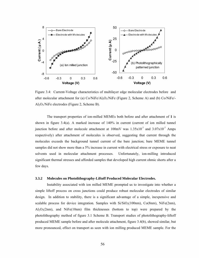
56
-8
-4
0
4
8
-0.6 -0.3 0 0.3 0.6Voltage (V)
Cur
rent
( μ
A )
Bare Electrode
Electrode with M olecules
(a) Ion milled junction
-50
-25
0
25
50
-0.6 -0.3 0 0.3 0.6Voltage (V)
Cur
rent
(μ A
)
Bare Electrode
Electrode with M olecules
(b) Photolithographically patterned junction
Figure 3.4: Current-Voltage characteristics of multilayer edge molecular electrodes before and
after molecular attachment for (a) Co/NiFe/Al2O3/NiFe (Figure 2, Scheme A) and (b) Co/NiFe/-
Al2O3/NiFe electrodes (Figure 2, Scheme B).
The transport properties of ion-milled MEMEs both before and after attachment of 1 is
shown in figure 3.4(a). A marked increase of 140% in current (current of ion milled tunnel
junction before and after molecule attachment at 100mV was 1.35x10⁻⁷ and 3.07x10⁻⁷ Amps
respectively) after attachment of molecules is observed, suggesting that current through the
molecules exceeds the background tunnel current of the bare junction; bare MEME tunnel
samples did not show more than a 5% increase in current with electrical stress or exposure to neat
solvents used in molecular attachment processes. Unfortunately, ion-milling introduced
significant thermal stresses and afforded samples that developed high current ohmic shorts after a
few days.
3.3.2 Molecules on Photolithography-Liftoff Produced Molecular Electrodes.
Instability associated with ion milled MEME prompted us to investigate into whether a
simple liftoff process on cross junctions could produce robust molecular electrodes of similar
design. In addition to stability, there is a significant advantage of a simple, inexpensive and
scalable process for device integration. Samples with Si/SiO2(100nm), Co(8nm), NiFe(2nm),
Al2O3(2nm), and NiFe(10nm) film thicknesses (bottom to top) were prepared by the
photolithography method of figure 3.1 Scheme B. Transport studies of photolithography-liftoff
produced MEME sample before and after molecule attachment, figure 3.4(b), showed similar, but
more pronounced, effect on transport as seen with ion milling produced MEME sample. For the

57
tunnel junction produced by photolithography and liftoff process, and whose data is presented in
figure 3.4 (b), current at 100mV before and after molecule attachment was 3.5x10⁻⁷ and 5x10⁻⁶
Amps respectively. These results strongly suggest that MEME samples, produced by via
photolithography-liftoff based approaches, contain a sharp perpendicular side plane that is
necessary for attachment of 1.
-0.15
-0.10
-0.05
0.00
0.05
0.10
0.15
-0.6 -0.4 -0.2 0 0.2 0.4 0.6Voltage (V)
Cur
rent
( µ
A )
Bare electrodeElectrode w ith molecules
Figure 3.5: Current versus Voltage behavior of Ta/Al2O3/Ta electrodes before and after molecular
attachment.
Another key merit of the MEME electrode design strategy is the ability to incorporate a
variety of metals that function as electrodes. Tantalum, a relatively unexplored metal electrode in
the field of molecular electronics, was utilized to construct photolithographically-defined cross
junction devices, in an attempt to improve the quality of the insulator layer of the electrodes.
Photolithography-liftoff produced MEME samples with (bottom to top) Si/SiO2 (100 nm), Ta (12
nm), Al2O3 (~2.5 nm), and Ta (12 nm) configurations were prepared and the transport behavior of
assembled devices measured in the absence and presence of 1, figure 3.5. Relative to bare
electrodes, molecular attachment affords a ca. 28 fold increase in the measurable current, due to
higher insulator film quality in the Ta system was observed; for the reported MEME current
before and after molecule attachment at 100mV was 6.4x10⁻¹⁰ and 1.8x10⁻⁸ Amps respectively.
Further current enhancement is anticipated assuming that the planar tunnel junction area can be
reduced to thinner line widths, from 5 µm to 0.065 µm that is currently possible via conventional
photolithographic approaches.
Molecular current is defined as the total current minus the current found for bare
electrodes. Given that the electrode junctions are ca. 5 μm long, are spaced 1 nm apart, and
average molecular width of 1 is ca. 2 nm, a closest-packed array of approximately 10,000

58
molecules can covalently attach to the exposed lengths (two sides) of the electrodes. At 50 mV
applied bias, the average current per molecule was estimated to be 0.16 (±0.13) nA per molecule,
for 48 photolithography-liftoff produced MEME samples, utilizing Ni and NiFe metal electrodes.
The experimental molecular current was of the same order but varied in absolute magnitude
between samples; a more useful measure of the variation in current per molecular between
samples is to examine the log [current (amps)] of -10.01 (±0.52) values. We tentatively propose
that the variation in calculated current per molecule values between samples arise from variations
in tunnel junction pattern edge quality. However, these edge variations are extremely small, when
compared to the current per molecule observed, and are much smaller than values reported for
most molecular electrodes devices.137,138
3.3.2.1 Control experiments:
A series of control experiments (i) Contact angle study to ensure metal-molecule surface
reaction, (ii) Effect of electrochemical treatment of electrodes in neat solutions and subsequent
rinsing, (iii) Reversible molecule attachment and corresponding change in current, (iv)
Attachment of short length n-butyl thio-acetate and long 20 carbon atom alkane dithiol chain and
(v) Increasing alumina thickness beyond the length of molecular bridge was performed to
demonstrate that the observed increase in current was due to the desired surface molecules
spanning across the MEME electrode rather than experimental artifacts resulting in uncontrolled
surface conduction.
To probe the presence of surface-bound molecules on NiFe electrodes contact angle
measurements (using water) were preformed on bare and 1-modified NiFe films.118 For
unpatterned thin films of NiFe, electrochemical treatment with CH2Cl2 solutions of 1 afforded a
contact angle changes from 11º to 54°; as control experiment, bare NiFe thin films were rinsed
with CH2Cl2 and 2-propanol under identical experimental conditions affording a modest increase
in contact angles (to 34°), presumably due to alcohol and/or hydroxyl substitution. This highly
water-insoluble molecule clearly functionalized the NiFe surfaces in a manner similar to previous
studies.118
In a second series of experiments, the MEME samples were subjected to CH2Cl2, cycled
potentiometrically in the absence of 1, and rinsed as previously described; no increase in current
was observed suggesting that 1 is necessary for charge transport in MEME tunnel junctions and
electrochemistry performed for molecule attachment does not change the conductivity of the
exposed edge tunnel junction.

59
-0.8
-0.4
0.0
0.4
0.8
-0.06 -0.03 0 0.03 0.06Voltage (V)
Cur
rent
( µ
A )
Bare TJ1st Molecules attachmentAfter 1st Au-S(1) exchange
( a )
-1.50
-0.75
0.00
0.75
1.50
-0.06 -0.03 0 0.03 0.06Voltage (V)
Cur
rent
( µ
A )
After 1st Au-S(1) exchange2nd Molecules attachmentAfter 2nd Au-S(1) exchange
( b )
-1.5
-1.0
-0.5
0.0
0.5
1.0
1.5
-0.06 0 0.06Voltage (V)
Cur
rent
( μ
A )
Bare Molecule attachedAfter attempt of exchanging Ni-S(1)
( c )
Figure 3.6: Reversible displacement of alkyl tether of 1 on Au electrode is observed upon
treatment with thiol Current-Voltage characteristics of a Ni/Al2O3/Au multilayer edge containing
1 and upon treatment with 5 mM 1-dodecanethiol. (a) Bare electrode before after molecular
attachment of 1 and after thiol exchange of tether from top electrode with the thiol group of 1-
dodecanethiol. (b) Repeat experiment using same sample: after first thiol exchange, 1 addition,
and after second thiol exchange reaction. (c) Ni/Al2O3/Ni molecular junction was not affected by
thiol exchange reaction. Bare electrode before after molecular attachment of 1 and after the
attempt to exhchange Ni-thiol bond. Au-S(1) and Ni-S(1) shows the bonding between metal and
thiol group of 1.
The most important control experiment was to show the reversibility of molecular
attachment across the electrode, and hence show that there was not any serendipitous breakdown
of the electrode at the time of molecular attachment. A MEME sample with Ni bottom and Au

60
top metal electrodes fabricated photolithography-liftoff method
(Ni(10nm)/Al2O3(2nm)/Au(10nm) configuration). The bond enthalpies for Ni-S and Au-S are
344 and 125 kJ/mol respectively.139,140 Since the Au-S bond is readily reversible, it was possible
to remove the thioacetate linkage by mass-action in a thiol-alkane solution, to form a self-
assembled monolayer of electrically insulating alkanes on the top Au metal electrode. We
postulate that this should disconnect the molecule from the top electrode and reduce current to the
background level of original electrode current without the molecules. Shown in figure 3.6(a) is
the I-V measurement of the bare electrode, after attachment of conducting molecule, and
following exchange of thiol group of alkyl tether of 1 with the thiol group of 1-dodecane thiol
after exposure to a 5 mMol solution of 1-dodecane thiol in ethanol for 45 minutes. The current
rose with molecular attachment then returned to the original bare electrode current level. The
cycle was repeated again, figure 3.6(b), and the same behavior was exhibited, demonstrating that
increase in current is due the molecular attachment across the insulator, not due to the
serendipitous breakdown of the insulator. A slight increase in current for the second functional
attachment was expected for an increased number of molecules due to second treatment. The
same displacement experiment performed on Ni/Al2O3/Ni electrodes did not show the effect of
thiol exchange reaction (i.e. a reduction in current) upon exposure to alkanethiol solution, figure
3.6(c). This is consistent with the thiol-Ni bond enthalpy being much stronger than Au, and
hence not reversible. This series of experiments also demonstrated that the molecular current was
not due to uncontrolled physisorption of molecules at the electrode surface. The use of a top Au
electrode offers chemical sensing possibilities since the top lead of a tethered conducting
molecule may be reversibly disconnected by coordination to a sterically bulky analyte molecule.
In our fourth control experiment we probed the effect of molecule with single thio-acetate
end group that was unable to bridge the insulating film of the exposed edge tunnel junction. For
this study 2 mM n-butane thio acetate solution in dicholoromethane was used to
electrochemically attach the short molecules on NiFe[12nm]/Al2O3[2.0nm]/ NiFe[12nm] tunnel
junctions. On 25 such tunnel junctions, a small increase of 17 ±16% over bare tunnel junction
current due to n-Butyl thioacetate was observed indicating that uncontrolled surface chemistry is
not responsible for conduction increase. For comparison bridging molecule 1 produced current
increases as high as 5000% over bare tunnel junction current on the samples prepared under the
same conditions. This experiment clearly suggested that just the formation of metal-thiol bond on
the surface is not sufficient to affect the conduction process of exposed edge tunnel junction
(MEME). We have also attached a 20 carbon long alkane with thio-acetate groups at each end to
span NiFe/Al2O3/ NiFe samples. A 2mM solution of this molecule in dichloromethane was used

61
in the process. Modest current increases of 84 ±57% change (20 samples) over bare MEME
current was observed consistent with the relatively poor conduction through an alkane tether
bridging the insulator gap.
In the last control experiment we saw that current increase on the exposed edge of tunnel
junction was only possible when the molecule was long enough to span the oxide barrier.
Molecule 1, was modified to have short hexyl thioacetate tethers resulting in an overall length
~2.4nm. For this study two MEME electrodes (NiFe/Al2O3/NiFe), first with ~2nm and the
second with ~3nm Al2O3 barrier thickness were used. Exposed edge tunnel junction with 2nm
thick Al2O3 (tunnel barrier thickness < molecule length) showed a clear increase in current, figure
3.7(a), but tunnel junction with 3nm thick Al2O3 (tunnel barrier thickness > molecule length)
showed no increase in current, figure 3.7(b). This further confirms that uncontrolled surface
chemistry does not provide a dominating current path.
Figure 3.7: Molecule with hexyl thio acetate tether (~2.4nm long) on NiFe/ Al2O3/NiFe
tunnel junction produced by scheme B. (a) molecule attachment on ~2nm thick tunnel
barrier (shorter than molecule length) (b) attachment on a ~3nm thick tunnel barrier
(thicker than molecule length).
3.4 Analysis of Electron Transport via Simmons Tunneling Model.
The electron transport properties of various MEME samples, with different insulator
thickness, in the presence and absence of 1, were analyzed via the Simmons tunnel current model.
By fitting observed current density (j)-voltage (V) data to the Simmons model within a medium
voltage range (V< φB/e) as shown below:50

62
⎪⎪
⎭
⎪⎪
⎬
⎫
⎪⎪
⎩
⎪⎪
⎨
⎧
⎥⎥⎦
⎤
⎢⎢⎣
⎡⎟⎠⎞
⎜⎝⎛ +−×⎟
⎠⎞
⎜⎝⎛ +
−⎥⎥⎦
⎤
⎢⎢⎣
⎡⎟⎠⎞
⎜⎝⎛ −−×⎟
⎠⎞
⎜⎝⎛ −
⎟⎠⎞
⎜⎝⎛=
deVmeV
deVmeV
dej
BB
BB
2/12/1
2/12/1
22
2)2(2exp
2
2)2(2exp
2
4ϕαϕ
ϕαϕ
π
h
h
h (3.1)
where m is electron mass, d is barrier thickness, φB is barrier height, V is applied bias , and α is a
unitless adjustable parameter, that allows for deviations from a simple rectangular barrier and
effective mass of the electron.51 Via equation 1, (setting α =1) we are able to fit the values of
both barrier height and barrier thickness before and after molecule attachment for various MEME
samples.
To validate the Simmons model in our system, a comparison was made between the
calculated thickness of alumina (present in bare MEME tunnel junction) from the Simmons
model and the physical thickness of a pattern of alumina (grown under identical conditions) as
measured by AFM. Calculated and measured thicknesses of alumina were in agreement within
the experimental uncertainty (2 Å). Moreover, the calculated values of barrier height of alumina
used in MEME samples closely matched barrier height values found for alumina films in other
studies of alumina tunnel junctions.138 It is important to note that Simmons model, originally
established for the simple tunnel barrier between two nonmagnetic metal electrodes, have been
used widely. There is plenty of literature available which justify the utility of this simple model in
many complex systems such as magnetic tunnel junctions and spin filters.141
For the modeling purposes, molecular current is defined as the total molecular electrode
current after molecule attachment minus the current of the bare electrode. The bare tunnel
junction area is 25 µm2 and an effective tunnel area for molecular current is calculated in
following manner. Via X-ray structural studies, 1 is approximately 1 nm wide (Fe-Ni edge), and
decorate the electrode edge in a closest-packed arrangement along a 10 µm insulator line as
shown in Figure 1b. Considering that the alkane tethers also occupy space, and that the cluster
core is insulated from its surrounds by the coordinated ligands, the most likely conduction
pathway is likely to be through the S(alkyl) chain. As a result charge enters and leaves the cluster
core and tunnels through the alkyl chains, giving a total molecular tunnel area of 1x10⁻¹⁰ cm2 (=10
µm x 1nm). Having obtained the current density for molecular barrier, barrier height and barrier
thickness were calculated using Simmons model as shown in equation (1). In order to check the
uniqueness of barrier height and barrier thickness values, curve fitting of experimental data to
Simmons model was accomplished in the narrow to very wide range of barrier thickness and
barrier height values. In both cases the values of barrier height and barrier thickness came out to
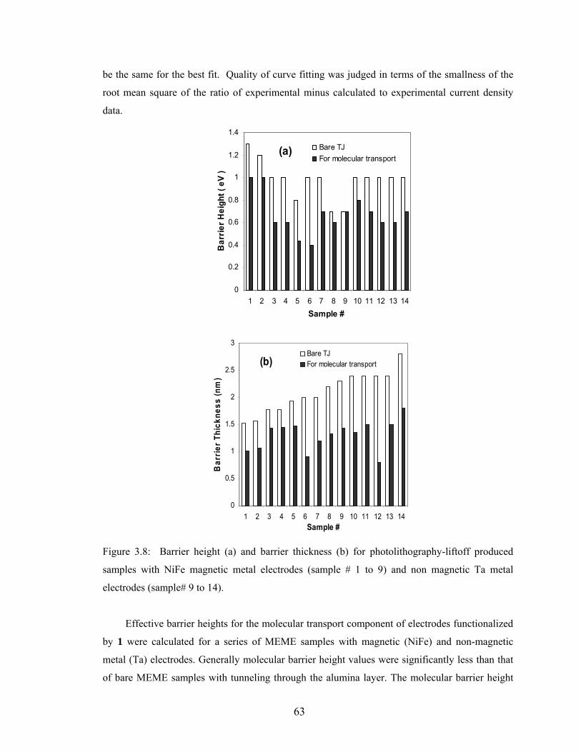
63
be the same for the best fit. Quality of curve fitting was judged in terms of the smallness of the
root mean square of the ratio of experimental minus calculated to experimental current density
data.
0
0.2
0.4
0.6
0.8
1
1.2
1.4
1 2 3 4 5 6 7 8 9 10 11 12 13 14Sample #
Bar
rier H
eigh
t ( e
V )
Bare TJFor molecular transport
(a)
0
0.5
1
1.5
2
2.5
3
1 2 3 4 5 6 7 8 9 10 11 12 13 14Sample #
Bar
rier T
hick
ness
(nm
)
Bare TJFor molecular transport(b)
Figure 3.8: Barrier height (a) and barrier thickness (b) for photolithography-liftoff produced
samples with NiFe magnetic metal electrodes (sample # 1 to 9) and non magnetic Ta metal
electrodes (sample# 9 to 14).
Effective barrier heights for the molecular transport component of electrodes functionalized
by 1 were calculated for a series of MEME samples with magnetic (NiFe) and non-magnetic
metal (Ta) electrodes. Generally molecular barrier height values were significantly less than that
of bare MEME samples with tunneling through the alumina layer. The molecular barrier height

64
values had significant variation with magnetic metal electrodes (0.67±0.3eV), but relatively less
variation was seen with the non-magnetic Ta metal electrodes (0.74±0.16eV), for the data shown
in graphs, as seen in figure 3.8(a). The scatter in current is presumably linked to spin effects of
the molecule coupled to magnetic leads and is currently being studied. In figure 3.8(b), the
barrier thickness (1.27 ± 0.27nm) calculated from the molecular I –V data is consistent with the
expected length of an insulating decyl tether. However, the overall molecular dimensions (via X-
ray) are estimated to be ca. 3 nm overall, due to 2 decyl tethers (ca. 1.2 nm length) and a
FeIII4NiII
4(CN)12 core (ca. 1 nm). The anticipated energy level diagram of the MEME before
and after attachment of 1, which resembles the energy diagram of expected for a double barrier
tunnel junction,142 is shown in figure 3.9.
Figure 3.9. Idealized band diagram of tunnel junction before (⋯) and after () attachment of 1.
Ef Fermi energy levels of metal electrode, where ~1 eV is the barrier height of the bare tunnel
junction, ~0.7 eV is the barrier height of the insulating alkane tether.
Evidence in support of molecule-mediated charge transport being the dominant
conduction pathway was obtained via temperature-dependent transport studies, obtained between
25 and 100oC, using photolithography-liftoff produced MEME sample [Ta (10 nm)/Al2O3 (2.5
nm)/Ta (10 nm)] . Temperature effects are possible only when molecular excitation, essentially

65
coupled to molecular transport, can be produced at the center of molecule; the tunneling transport
mechanism through the alumina insulator and alkane tether is essentially temperature
independent.51 Upon heating, the sample current increases, corresponding to a thermally activated
transport process, with a ca. 0.30 (±0.02) eV activation energy barrier. This estimated activation
energy barrier is consistent with activation energies expected for conformational changes143 and
calculated transport activation energies reported for other molecules.144 The data also suggests
that the transport mechanism is more complicated than a simple elastic tunneling process
(thermally assisted tunneling) but is consistent with the idealized molecular geometry on the
electrode surface proposed. Our molecule which has two tunnel barriers ( due to alkane tethers )
separated by organometallic cube with conjugated bonds, which provide density of states closer
to metal electrodes Fermi level145. For small area double tunnel barrier system it is reported that
both elastic and inelastic process contribute to the current and direct tunneling is more prominent
towards lower temperature range.146 In the transport study of several single molecular magnets
transition between pure quantum tunneling (temperature independent) to thermally assisted
tunneling (temperature dependent) was observed.147 Due to adverse thermal stresses on MEME
stability we are currently unable to perform cryogenic transport studies. However, the cutoff
temperature for several molecular systems are close to room temperature, e.g. for terphenyl and
nitroazobenzene molecules thermally activated conduction process freeze out near 10 degree C.144
Temperature studies of these molecular junctions are ongoing and largely limited by the control
of film stresses during the growth process.
Moreover, additional support for a qualitative tunneling conduction model can be
inferred from the calculated value of the tunneling decay coefficient (β).148 An exponential
decrease in current (I ∝ exp(-βd)) with alkane length (d) was commonly measured. Here β was
extracted from our calculated barrier heights from the Simmons model for nonmagnetic MEME
samples whose barrier properties are given in Table 3.1. We experimentally observed a β of 0.88
(0.10) Å-1, which was remarkably close to the observed value of β = 0.85 Å-1 for alkane tether of
similar lengths as seen in STM studies 148 of individual molecules and from self-assembled
monolayers of thiol alkanes.51,148 Here it is worth noticing that we are comparing our the value of
β, which is for 10 carbon long alkane tether, with the β of 10-12 cabon long alkane studied
elsewhere.

66
Table 3.1 Barrier thickness and height estimated via Simmons tunnel current model fits of
conduction through assembled Ta/Al2O3/Ta multilayer edge molecular electrodes.
Barrier Thickness (nm)
Barrier Height (eV)
Bare Electrode Tunnel Barrier 2.48 (±0.18) 0.94 (±0.13)
Molecular Tunnel Barrier 1.30 (±0.29) 0.74 (±0.16)
On the basis of experimental observations we have come up with following qualitative
model for the transport through 1. In our study molecular junction is comprised of two tunnel
barrier and one region of supposedly fast transport. Time of charge transfer through the molecule
has three components: [1] tunneling of electrons from the left ( or right) metal electrode to the
organometallic cube present in the center of molecule, [2] quick charge transport through
organomettalic cube and [3] Tunneling from the organometallic cube towards right (or left) metal
electrode. Expression for the total time of charge transfer (tTotal ) through molecular junction is
given by following equation :
ttttTotal 321 ++= (3.2)
t1, t2 and t3 are the inverse of charge transport rate through first alkane tether,
organometallic cube, and second alkane tether respectively. In the equation (3) transport
rate through alkane tethers, which is based tunneling process and supposed to be the same
in both alkane tethers, is expected to be much slower than transport rate through
conjugated bonds enriched organometallic cube of 1.145 Which implies that t2<<t1 and t3.
Putting t1=t3=1/r(alkane), where r(alkane) tunneling rate through
( )alkanertTotal
2≈ (3.3)
Molecular transport rate can be written as
)(alkanerRate ∝ (3.4)
According to our experimental observations, molecular transport rate through 1 is governed by
the slowest transport rate which is the tunneling process through alkane tethers.

67
3.5 Conclusions
By using the exposed face at the edge of a multilayer thin film pattern, an electrode with
nm-scale distance between metal leads was reliably formed. Importantly, the critical dimension
was controlled to molecular lengths with angstrom scale precision using conventional deposition
processes. Since the pattern can be defined by photolithography, the economical large scale
integration of molecular electrodes can be readily achieved, using the described approach. In our
study, molecular electrodes with insulator thicknesses ranging from 1.5 to 2.5nm were studied.
The cross junction array can utilize recently developed two terminal logic designs130 or
alternatively, the edge geometry can be incorporated into more conventional, arbitrarily addressed
junctions. This edge geometry does not readily incorporate an electrostatic gate at close
proximity, however, electrostatic switching of molecules typically requires extremely high
electric fields (~100 MeV/cm),143 that far exceed the breakdown point of known dielectrics. This
two terminal device architecture approach has two major merits other than ease of integration.
First, a wide range of materials can be introduced on alternate sides of an insulating barrier,
including magnetic materials, allowing for the possibility of current modulation via spin state of
the bridging metal cluster. Second, all conductive molecules reside on the exposed surface
allowing for strong selective chemical interactions with analyte molecules. In principle, a bound
analyte molecule can change the conformation of the conduction molecule, or force the reversible
removal of a tether from a top gold contact, which may lead to the design of a reversible sensing
device. Furthermore, the planar electrode geometry also provides for further conformational
constraint of the molecule on the surface, which may be an important consideration in improving
the molecular conduction process. The relative simplicity of this electrode geometry allows for a
significant improvement in the ability to study molecular conduction and may finally enable
molecules to be incorporated into large scale device architectures. We have observed that
molecular electrode fabrication scheme can further simplified by avoiding the deposition of
aluminum; in the next chapter we present a method in which a controlled oxidation was utilized
to produce novel molecular electrodes.

68
Chapter 4
Molecular Scale Electrodes Fabricated By Single Step Oxidation of Photolithographically
Defined Metal Electrodes
4.1 Introduction
The ability of chemical synthesis to control the electronic, magnetic and optical
properties of molecules has motivated extensive research in the field of molecular devices.8
Integrating molecules into devices by connecting the molecules between two metal electrodes
remains one of the most difficult challenges to producing novel electronic, optoelectronic and
spintronics devices.8,149 To date, several schemes for producing 2-10 nm gaps have been
reported.150 Electro-migration produced break junctions and mechanical break junctions possess a
nm gap between two electrodes of the same metal .109 Several molecular transport studies
exhibiting, negative deferential resistance,149 Kondo effect39 and current suppression,33 have been
performed with the low yield and difficult to reproduce break junctions .103 Controlled growth of
metal electrodes during a chemical vapor deposition 151 and an electrochemical process152 was
successfully demonstrated to produce nanogaps. Under these approaches the gap between two
distant electrodes was reduced by amassing the electrode materials controllably.
Guo et al. have successfully produced molecular dimension gap on a single wall carbon
nanotube. Oxygen plasma and chemical fictionalization were utilized, respectively, to burn a
≤10nm segment of carbon nanotube and to produce a molecular bridge between two ends of the
nanogap. 153. In molecular lithography process, multi-step and time intensive chemistry was
performed to use the molecular monolayer to set the nanogap between two metal electrodes .150
Moreover, utilization of carbon nanotube based shadow154 and complex E-Beam alignment155 are
promising approaches for producing a nanogap between two metal electrodes.
Prevailing schemes to produce molecular dimension gaps are complicated and limited in
scope as only few metals, mainly unoxidizable gold which is amenable for molecular self
assembly, can be used as metal electrodes.39 In most of the cases, it is not possible measure
transport through the molecular-scale electrodes without a molecule; this factor makes many
molecular studies questionable and care must be taken to avoid formation of nanoparticles with
Coulomb blockade.103 Another important issue is associated with the strategy of attaching
molecules to the electrodes. Typically covalent bonds of a sheet of molecules to the bottom
electrode are made by self assembly followed by direct deposition of the top metal electrode.137
However this can complicate the molecular transport study by magnifying the effect of metal-
molecule contacts and shorting defects. Uncontrolled impurities from the solution during self

69
assembly process and diffusion of metallic atoms into self-assembled molecular layer during top
metal electrode may mask the true behavior of molecules.
A promising route to produce the molecular dimension gap between two electrodes is by
controlling the thickness of a robust yet 1-3nm thick insulator between top and bottom electrodes.
At the edge of the photolithographically defined junction pattern there is a vertical edge of
exposed metal/insulator/metal structure. The minimum physical thickness between two electrodes
is the thickness of insulator and is easily tuned to the length of molecular clusters. Covalent
bonding of molecular clusters on the exposed edge of tunnel junction can establish molecular
conduction channels. Critical to this approach is keeping tunneling current via insulator in the
planar junction area very small allowing the molecular conduction to dominate. A scheme similar
to the hypothesis of insulators giving precise thickness control is based on etching of ~4 nm
silicon di-oxide insulator present between two Si or metallic layers. The etching step is followed
by the shadow controlled metal depositions to shorten a nm gap between two metal or Si
electrodes to produce molecular dimensions gap.110,156 This approach is likely to suffer with
irreproducibility with pattern edge line roughness and may be difficult to produce in the large
array. The concept of producing molecular junctions through film thickness control, without
reducing a ~4nm gap to molecular dimension by shadow metal deposition, has been successfully
demonstrated in a recent work .109,111 The later submitted communication,111 utilized an exposed
edge tunnel junction with ~3.5nm insulator and gold top and bottom electrodes. Instead of
shortening the gap between two electrodes via shadow mask metal deposition, several units of a
short molecule were compounded to bridge the insulting gap between two electrodes. These
molecular bridges formed a necklace around preformed tunnel junction. This resulted in >2 order
increase in transport over the bare tunnel junction. However, in this approach insulator film
thickness is still more than the length of molecules of interest (<3nm). For long conjugated
organic molecules rotation conformation of π bonds can dramatically reduce the current. A more
ideal molecular geometry is to have nm-scale tethers connecting a molecular cluster between
leads. Tether lengths >1nm will have difficulty as too long a conduction barrier. One such Octa
Metallic Cluster (OMC) with thiol-alkane tethers has been recently synthesized and incorporated
in a.multilayer edge molecular electrode (MEME)geometry .109 We successfully produced a gap
as low as ~1.5 nm between a two metal layers on the exposed sides of a metal-alumina-metal
tunnel junction. We utilized several meals, such as Ni, NiFe, Au and Ta, to produce molecular
junctions. A molecular dimension gap is controlled by the thickness of aluminum deposition (and
subsequent oxidation step). An exposed metal-insulator-metal face at the pattern edge is produced
by the direct ion milling or liftoff step. Electrode fabrication is followed by the electrochemical

70
self assembly of OMC produced two arrays of molecular bridges spanning the insulator.109
Modeling the conduction process resulted in a rate limiting step of tunneling into/out of the
metallic core through alkane tethers. Interestingly, the molecular conduction process was limited
by the length of the alkane tether and was rather insensitive to the tunnel barrier thickness; barrier
height mainly affected the background planar area tunnel current. Ability to tune tunnel barrier
thickness allows a simpler oxidation step and relaxes the requirement for ultra uniform insulator
metal conformal coverage.
In this chapter we describe a simpler oxidation controlled method to produce a molecular
length gap between tantalum (Ta) and an arbitrary top metal electrode. An advantage of this
approach is that only one step oxidation of the bottom electrode, without depositing additional
insulator or oxide forming metal film, produces the nm thick tunnel barrier. Deposition of the
second metal electrode with its dimensions matching with the oxidized region of the bottom Ta
layer produced a Ta/TaOx/metal junction with the exposed edges. Molecular transport studies
before and after molecule attachment and a number of control experiments are utilized to
demonstrate the successful realization of the new class of molecular electrodes.
4.2 Experimental Details:
Figure 4.1: Fabrication steps: deposition of bottom electrode of ~10 nm Ta (a), opening a window
in photo resist to expose selective area of bottom electrode(b), plasma oxidation to produce TaOx
(c) followed by top metal electrode deposition (d). Liftoff of photoresist produced tunnel junction
with exposed edges (e). A 3D image of a Ta/TaOx/M electrode before (f) and after (g) molecule
attachment. X-Ray crystallograph for the octametallic molecular cluster used in this study (h).
71
The Ta/TaOx/M electrode fabrication scheme is summarized in figure 4.1. A (100)
silicon wafer with 100nm thick thermally grown silicon di-oxide was used as a substrate and
cleaned by organic solvent rinse. Sputter deposition (using AJA International sputtering machine)
of the bottom Ta metal electrode was performed, with 2x10⁻⁷ torr base pressure, 100W gun
power, and 1mtorr argon pressure. The following step was the photolithography (with Karl-Suss
Mask aligner) for the creation of photoresist (PR) mask, using Shipley 1813, with a 5µm wide
window over a Ta bottom electrode, figure 4.1(b). Soft baking of PR, performed at 110 ºC, was
critical for strengthening the PR to minimize its burning in the following plasma oxidation step.
Plasma oxidation of the Ta electrode through a 5µm window was performed, figure 4.1(c), within
the sputtering chamber at 60 mtorr pressure of argon and oxygen mixture (Argon:Oxygen::1:1)
and 20W RF substrate bias for 30-90 seconds duration .109
The growth rate of TaOx has two competing factors, growth due to oxidation of Ta atoms
and etching due to sputtering by the bombarding ions from plasma .157 Plasma oxidation condition
was carefully optimized to have the desired thickness of high quality TaOx insulator and to burn
the photoresist protection minimally. According to AFM study of oxidized patterns, the PR etch
rate was found to be 30±4 nm per minute.
After the plasma oxidation process, a top metal electrode was deposited, through the
same PR window as utilized for the oxidation step. This approach enables the coverage of only
the oxidized Ta metal present in the exposed region within PR window, figure 4.1(d). Various
metal, such as Ta, palladium (Pd) and NiFe (with Ni:Fe: 80::20), were utilized as top metal
electrode. It is noteworthy that at the end of tunnel junction fabrication we observed a nonlinear
tunneling electron transport on bare tunnel junction. The tunneling behavior is only possible when
the top metal electrode and the unoxidized part of the Ta electrode are disconnected.
Fabrication of the bare Ta/TaOx/M electrode was followed by the molecule attachment.
Two molecules, cyanide-bridged octametallic molecular complexes (OMC), [(pzTp)FeIII(CN)3]4-
[NiII(L)]4[O3SCF3]4 [(pzTp) = tetra(pyrazol-1-yl)borate; L = 1-S(acetyl)tris(pyrazolyl)decane]3
and 1,n-Dithiol Eicosane (HS(CH2)20SH),158 were synthesized. Via thiol surface attachment to the
metal leads, an array of OMC or Dithiol Eicosane molecules were covalently-linked onto the Ta
and top metal electrodes, forming a dominant conduction pathway. Electrochemical molecular
attachment 117 of the molecules to the Ta/TaOx/M electrodes via the thiol group was
accomplished by the immersion of the electrodes in a dichloromethane solution of molecules
(0.1mM), followed by alternating a ±100 mV bias between the two metal electrodes at a time
interval of 0.002 seconds for 2 min.109 Subsequently, the assembled devices were rinsed with
dichloromethane, 2-propanol, and deionized water and dried under a nitrogen gas stream.

72
Immersion of the electrodes in a dichloromethane solution of molecules without the performing
of the electrochemical step did not affect their transport properties. We surmise that the use of
alternating voltage during the electrochemical step, in addition to removing thio-acetate
protection group, helped condition the metal electrode surface by slightly etching it and
subsequently favored the metal-thiol bonding.
Transport study of the Ta/TaOx/M electrodes was performed before and after the
attachment of molecules using a Kiethley. Normally current-voltage measurement on Ta/TaOx/M
electrodes, before and after molecule attachment, was performed between ±100 mV. However, a
±500mV range for transport studies was chosen for determining the tunnel barrier properties. It is
noteworthy that chosen voltage ranges are far below the breakdown voltage potentials (~1.7V) of
the bare electrodes. Typically 3-5 measurements per each I-V plot, using a 5 mV voltage step and
0.5 to 1 second time steps, were collected for each sample, to minimize possible scan to scan
variation error.
Figure 4.2: Junction characterization: (a) SEM micrograph giving top view and (b) 3D AFM view
of one side of a Ta/TaOx/Ta electrode.
Structural characterization of typical Ta/TaOx/Ta electrodes by SEM, figure 4.2(a), and
AFM, figure 4.2(b), showed the expected edge geometry and dimensions of the junction.
Tunneling current transport study was found to be the best indicator of the tunnel junction quality.
Effective barrier thickness and barrier height were measured by fitting the transport data of a bare
Ta/TaOx/M electrode with the Simmons model.159 Typical junction area ranged from 9-25 µm2.
Breakdown voltage and barrier thickness of electrodes were 1.7±0.2 V and 2-3.5 nm,
respectively. The fact that tunneling current was observed meant that there was no deposition ot
top metal directly on the bottom electrode and that nm-scale gaps between electrodes existed.

73
4.3 Results and discussion:
-120
-60
0
60
120
-0.6 0 0.6Voltage (V)
Cur
rent
(nA
)
Bare Ta/TaOx/TaOMC
(a)
-250
-125
0
125
250
-0.6 0 0.6Voltage (V)
Cur
rent
(nA
)
Bare TaTaOxNiFeOMC
(b)
-1.5
-0.75
0
0.75
1.5
-0.6 0 0.6Voltage ( V )
Cur
rent
( μ
A )
Bare Ta/TaOx/NiFew ith C20 alkane
(c)
Figure 4.3: Transport before and after molecule attachment: (a) I-V before and after OMC
attachment on Ta/TaOx/Ta and (b) Ta/TaOx/NiFe. (c) Ta/TaOx/NiFe before and after Dithiol
Eicosane molecule attachment.
Transport of Ta/TaOx/M electrodes before and after molecule attachment was studied.
The Ta/TaOx/Ta electrode exhibited a 3-5 fold increase in current due to OMC attachment, figure
4.3(a), and Table 4.1.
Table 4.1: The magnitude of current at 100mV of electrode in bare state and after molecular
bridging.
Bare (nA) With molecule (nA)
Ta/TaOx/Ta [figure 3 (a)] 2.4 11.7
Ta/TaOx/NiFe [figure. 3(b)] 3.2 20.1
Ta/TaOx/NiFe [figure. 3(c)] 53 104
Molecular current is defined as total current minus bare electrode current. To show the
ability of Ta/TaOx/M electrodes to produce a nanogap between dissimilar metal electrodes, the

74
top Ta metal electrode from the Ta/TaOx/Ta electrode was replaced with the ferromagnetic NiFe
to produce a Ta/TaOx/NiFe electrode. OMC attachment on these junctions yielded a 3-7 fold
increase in current over the background current, a representative example is shown in figure
4.3(b). With the utilization of NiFe as a top electrode ~30% higher current is seen.
Attachment of short length 20 carbon alkane molecules, Dithiol Eicosane, also increased
the current of Ta/TaOx/NiFe by ~2 fold, figure 4.3(c). Dithiol Eicosane were found to be
attaching rather easily on electrodes prepared with smaller oxidation time, 30-40 seconds, which
presumably produces a smaller insulating gap between two metal electrodes within and, more
importantly, at the edge of the tunnel junction. The present scheme allows the realization of a
shorter insulating gap between unoxidized bottom Ta electrode and top NiFe electrode compared
to Al2O3 deposition of insulator barrier. Consequently, this situation enables the bridging of
shorter Dithiol Eicosane molecules (~2.2nm) between metal electrodes. However, generally,
Ta/TaOx/NiFe junction with produced with smaller oxidation time duration exhibited higher
leakage current. It is noteworthy that here barrier thickness of Dithiol Eicosane is comparable
with TaOx barrier thickness; thus increase in current is due to the establishment of new relatively
conductive molecular channels. The leakage current through ultrathin TaOx varied from sample
to sample. Plasma oxidation is expected to produce inhomogeneous oxide;160 it is difficult to
reproduce the effect of imperfect stoichiometry on samples grown in different batches.
Approximate number of OMC’s (1nm diameter) attached on Ta/TaOx/M electrodes 10um
length) is ~10,000; however, due to smaller steric hindrance the number of Dithiol Eicosane
molecules attached on electrodes is expected to be ~30,000. The magnitude of the current per
molecule, calculated according to (total current - bare electrode current) / (# of molecules) ,109 for
OMC and Dithiol Eicosane were 12±6.7pA and 0.62±0.5pA, respectively. The current per
OMC(Dithiol Eicosane) molecule with NiFe/Alox/NiFe electrodes was 160±130pA(11±7pA);109
change of metal electrode from Ta to NiFe exhibits an increment by a factor of ~17 for
OMC(Dithiol Eicosane). More than one order difference in current per molecule between two
metals can be attributed to the difference in availability of number of sites for molecule
attachment or metallic density of states .161 Since Ta is easily oxidized, it also possible for a
partially oxidized surface to have fewer molecular channels than the case with NiFe electrodes.
However it is difficult to distinguish from contact/electrode effects and the current density
calculations are based on the total exposed electrode edge area. The current per molecule (50 mV
bias) of OMC across Ta/AlOx/Ta electrode,109 (3.5±2pA), is in good agreement with the present
case of the Ta/TaOx/Ta electrode (11±7pA).

75
4.3.1 Control experiments
0.0
2.0
4.0
0 0.25 0.5Voltage (V)
Cur
rent
( µ
A )
Bare Ta/TaOx/PdWith OMC
(a)
0
0.03
0.06
0 0.25 0.5Voltage ( V )
Cur
rent
( n
A )
Bare Ta/TaOx/NiFeAfter OMC
(b)
0
60
120
180
0 0.25 0.5Voltage (V)
Cur
rent
( n
A )
Bare Ta/TaOx/NiFeWith pure solvent
(c)0
200
400
0.00 0.25 0.50Voltage ( V )
Cur
rent
( n
A )
Bare Ta/TaOx/NiFeWith Dodecane thiolWith dodecane thiol
(d)
Figure 4.4: Control experiments. Ta/TaOx/M electrodes with (a) high leakage current and (b)
with thick tunneling spacer, produced through PR protection with undercut profile, are unaffected
by OMC attachment. (c) Electrochemical molecule attachment process in pure solvent produced
no change on transport. (d) Attachment of 1,n dodecanthiol thiol molecules produced ± 15%
change in the bare Ta/TaOx/NiFe electrodes transport.
A number of control experiments were performed to confirm that conduction was through
molecules spanning the insulator surface of the electrodes. Electrodes with large leakage current,
for instance Ta/TaOx/Pd with 200kΩ junction resistance, remained unaffected by the molecular
treatment. High junction conductivity signifies the high leakage current between two metal
electrodes via a presumably thinner and/or defective TaOx barrier;162 establishment of new
molecular channels will only contribute negligibly with respect to the bare junction current.
Ta/TaOx/M electrodes with a thicker tunneling barrier than the physical length of OMC
did not exhibit any noticeable change in transport. To perform this experiment, the top
electrode/oxide photo resist mask was made with an undercut. The idea of using undercut in PR

76
mask was to create a sufficiently large gap (>3nm, the OMC length) between the top metal
electrode and the unoxidized part of the Ta electrode. This precludes the possibility of producing
shorter OMC molecules spanning the gap to form addition molecular current. Isotropic plasma
oxidation of Ta film produced a wider TaOx span as compared to the width of the top metal
electrode deposited by an approximate line-of-sight deposition conditions. We were unable to
resolve the lateral dimensions of the larger gap, but conclude that it is greater than 3 nm.
In the next control experiment, the possibility of any degradation of electrodes during
electrochemical treatment (HCl formation) was determined. Electrochemical process, with the
pure dicholoromethane solvent, did not exhibit any noticeable change in the transport of bare
electrodes as shown in figure 4.4(c).
Attachment of a 1-n dodecanthiol from its 2mM solution in dicholoromethane on a
Ta/TaOx/NiFe electrode nominally affected bare electrode transport (±15%), figure 4.4(d). This
experiment confirms that only a long molecule that can bridge over the insulator and form metal-
thiol chemical bonds are responsible for observed current increase.
4.3.2 Transport-Analysis
0
0.5
1
1.5
2
2.5
Barrier Height (eV) Barrier Thickness(nm)
Bare Ta/TaOx/Ta el. OMC Dithiol Eicosane
(a)
Figure 4.5: Barrier height and effective barrier thickness before and after OMC and Dithiol
Eicosane attachment as calculated from Simmon’s model fit to experimental data. (b) Schematic
description of change in tunneling barrier specificity of bare electrode after molecule attachment.
To elucidate the molecular conduction mechanism, we have fitted current density (j)-
voltage (V) data of bare and molecule attached Ta/TaOx/Ta, electrodes with the Simmons model
.159 We surmise that ~10,000 nm-scale molecules, coupled to metallic electrodes by the well
defined metal-S bonds, are capable of affecting the transport of Ta/TaOx/M electrodes. The

77
molecular current was calculated by subtracting the bare electrodes current from the total current
observed after the molecule attachment. A molecular cross section area is calculated by assuming
that 10,000 OMCs, each with 1nm square, are attached along the 10µm long edge giving 1x10⁻¹⁰
cm2 area for molecular current. Although a larger number of Dithiol Eicosane molecules are
expected to bridge between two metal electrodes, they are expected to pack within the same
physical area as calculated for the OMC molecules.
Barrier properties, barrier thickness and barrier height on the bare and molecule attached
electrodes were obtained by fitting the experimental current density -voltage data with the
Simmons model within a medium voltage range (V< φB/e) as give below163:
⎪⎪⎪
⎭
⎪⎪⎪
⎬
⎫
⎪⎪⎪
⎩
⎪⎪⎪
⎨
⎧
⎥⎥⎦
⎤
⎢⎢⎣
⎡⎟⎠⎞
⎜⎝⎛ +−×⎟
⎠⎞
⎜⎝⎛ +
−⎥⎥⎦
⎤
⎢⎢⎣
⎡⎟⎠⎞
⎜⎝⎛ −−×⎟
⎠⎞
⎜⎝⎛ −
⎟⎠⎞
⎜⎝⎛=
deVmeV
deVmeV
dej
BB
BB
2/12/1
2/12/1
22
2)2(2exp
2
2)2(2exp
2
4ϕαϕ
ϕαϕ
π
h
h
h(4.1)
where m is electron mass, d is barrier thickness, φB is barrier height, V is applied bias , and α is a
unitless adjustable parameter, that allows for deviations from a simple rectangular barrier and
effective mass of the electron.163 Via equation 1, (setting α =1) we are able to fit the values of
both barrier height and barrier thickness before and after molecule attachment for various
Ta/TaOx/Ta samples. Tunneling decay factor (β) was also calculated using barrier height data.
The Molecular cluster possesses a relatively conducting organomettalic cube .3 Transport
rate via molecular cluster has three stages: slow tunneling rate(s) from metal electrode (OMC
center) to OMC center (metal electrode) and fast transport within organometallic cube.109 The
molecular barrier thickness is expected to be equal to one alkane tether length (~1.2 nm) while
total molecule length is ~3nm. The Simmons model clearly suggests that for OMC barrier
thickness is ~1.3nm and barrier height of ~0.72 eV in accordance with a previous molecular
transport study with the same molecule .109 Tunneling decay factor for the transport through
OMC came out to be 0.86 Å-1 which is in agreement with the previously obtained β for the 10-12
carbon alkanes.163 For Dithiol Eicosane molecules, similar analysis was performed. Barrier
thickness, barrier height and β were 1.8±0.1nm, 0.55±0.05 eV and ~0.75Å-1, respectively
Attainment of shorter barrier thickness with regards to the physical length of Dithiol Eicosane ,
~2.2nm, can be attributed to the deviation of barrier shape and mass of the electron from the ideal
case.163 Change in molecular conformation is another likely reason for the smaller barrier
thickness.

78
4.4 Conclusion
A molecular-scale gap between two metal electrodes was successfully controlled by a
single step plasma oxidation method. This simple approach only required widely available thin
film deposition method and photolithography. A variety of metals can be used as the top electrode
with present electrode design. The primary advantage of this methodology is that it produces a
lateral-insulating gap smaller than ~2nm. This gap does not have to be precisely controlled to the
molecular length so long as the molecule can bridge it and background tunnel current is
sufficiently low. The present device design will directly benefit from the commercially available
scaling of photolithographic line width w (5um to ~50nm), with background tunnel current being
proportion to w2 and molecular current proportional to 1/w. Conduction is through the well
controlled length of a molecule, allowing chemical synthesis to directly affect conduction which
is not possible in polymer systems or large macromolecules where π bond conformations are
dominate. This devise design allows molecules in the exposed region of the junction to easily
interact with light radiation and specific chemical agent (that can affect the molecular transport)
allowing the formation of molecular-photo devices and chemical sensors, respectively.

79
Chapter 5
TaOx Thin Film Photovoltaic Devices
5.1 Introduction
The realization of thin film based photovoltaic devices offers lucrative options for the
replacement of costly silicon based solar cells.164 A practical thin film based solar cell should be
able to absorb sufficient radiation. More importantly, it should be endowed with a mechanism,
akin to the inbuilt potential in the p-n junction solar cells,165 to separate the photo-energy created
electron-hole pairs. Device, based on ~100nm thick semiconducting cuprous oxide (Cu2O)
sandwiched between the two metal films have exhibited rectifying transport properties and
photovoltaic effects.166 Rectification in this case was attributed to the dissimilar metal contacts
with different work functions present on the two sides of Cu2O.167,168 However, the maximum
solar cell efficiency achieved thus far with Cu2O based solar cell is ~2%, which is well below the
predicted efficiency for Cu2O based solar cells (20%).168 The aim of using ~100nm thick Cu2O,168
primarily to enhance the light absorption, is generally defeated as it possesses atomic defects in
the proportion of thickness. A higher defect density can annihilate the photo-generated electron-
hole pairs before they are separated and transferred to the opposite electrodes.164,165
A better approach to make a metal-metal oxide-metal based solar cell is to reduce the
metal oxide thickness to a few nm, yet managing to keep the light absorbance reasonably high.
Recently, attempts have been made to produce a thin film photovoltaic cell using an ultrathin
~3nm niobium oxide (NbOx) based tunnel barrier, grown by the air oxidation of niobium (Nb).169
The significant difference in the barrier heights of the two metal/insulator interfaces of the
Nb/NbOx/Ag tunnel junction was attributed to the difference in the work function of the metal
contacts. In spite of showing a rectifying behavior, these tunnel junctions did not show a
noticeable photovoltaic effect. Previously, tunnel junctions utilizing aluminum (Al) electrodes
and 3nm alumina (AlOx) with an Al/AlOx/Al configuration have exhibited ~0.9eV difference in
barrier heights at two Al/AlOx interfaces.165 This study suggested an inhomogeneous oxidation
alone can produce an inbuilt potential, i.e. the difference between the two barrier heights. In our
knowledge, no photovoltaic effect has been reported with the Al/AlOx/Al system. The reason
why this system did not show photovoltaic effect is presumably due the absence of a mechanism
to absorb the light radiation within the AlOx barrier.
In the quest of finding a significant photovoltaic effect in the metal-metal oxide-metal
system, we explored the photovoltaic effect in Ta/TaOx/Ta tunnel junctions. This system is
particularly promising; previous X-Ray photoelectron emission (XPS) studies of Tantalum oxide

80
(TaOx), grown by the thermal oxidation of a Ta metal, exhibited a graded distribution of
unoxidized Tantalum (Ta) ions impurities.160 The gradient of atomic defects within a TaOx is
consistent with the oxygen diffusion model. We conjectured that a similar profile of atomic
defects will appear from the plasma oxidation treatment157 of Ta. The reason for switching to
plasma oxidation instead of thermal oxidation is its easy controllability to produce ultrathin
insulators. 17 We hypothesized that defects at the optimum spatial location within TaOx can
absorb light radiation170 to form electron-hole pairs. On the other hand, a gradient in defect
density162,171 can produce the difference in the barrier height between the two Ta/TaOx interfaces.
Eventually unequal barrier heights165 will produce inbuilt electric fields for the separation of
electron–hole pair.172 To realize this theme, we have produced a Ta\TaOx\Ta tunnel junction
using photolithography, sputter deposition, and plasma oxidation. A highly controllable plasma
oxidation process produced nm thick nonstochiometric TaOx.171 The number of characterizations,
including the transport and optical properties of TaOx, were utilized to establish these junctions
as a photovoltaic device.
5.2 Experimental details:
Figure 5.1: The fabrication and characterization of Ta/TaOx/Ta junction: (a) Photoresist pattern
for bottom Ta layer deposition; (b) pattern after deposition of Ta film and lift-off of photoresist;
(c) after the second stage photolithography; (d) plasma oxidation of Ta (dark black region shows
oxidized segment) layer followed by the deposition of the top Ta electrode in the white area; (e)
planar view of the complete junction after liftoff; (f) SEM micrograph of a Ta/TaOx/Ta junction,
and (g) AFM study of the bottom electrode.
(f) (g)
81
The fabrication steps of Ta/TaOx/Ta junctions and their characterization is illustrated in
figure 5.1. Throughout this study, a Si wafer with thermally grown 100nm silicon oxide was
utilized. Wafer pieces were sequentially washed in acetone, isopropyl alcohol, and DI water for
2min each and then samples were dried in the nitrogen flow.
The following steps were performed in the given order during first stage
photolithography: the spin coating of a Shipley 1813 positive photoresist at 3500 rpm for 30sec,
soft backing at 100ºC for 1 min, exposure for 20sec through a photomask by Karl-Suss mask
aligner, the developing of a photoresist with a MF-319 developer solution for 1min, and the
rinsing of the samples in DI water 5 times followed by drying in the nitrogen gas flow. The
samples were then transferred to the load lock chamber of the sputtering machine (AJA
Multitarget Sputtering System) using clean sample enclosures. The sputtering of ~12nm Ta was
performed in the main chamber with 2x10⁻⁷ torr base pressure at 100W DC gun power and 1
mTorr Ar (99.99% purity) pressure at RT. Within 5 min of the sample’s removal from the
sputtering machine, it was soaked in a Shipley-1165 resist remover solution for 30min for liftoff,
followed by rinsing in DI water and drying in the nitrogen flow.
The second photolithography step, using the previously mentioned photolithography
protocol, to produce a cross pattern, figure 5.1(c), was performed. Next, samples were transferred
to the sputtering machine. The duration of which the first Ta film remained outside of the
sputtering system was 2hrs (for 90 min in contact with various electronic grade solvents and for
30min in the clean room environment).
The exposed segment of the bottom electrode through a photoresist layer was plasma
oxidized to produce a ~3nm TaOx insulating layer. The thickness of TaOx was confirmed by the
spectroscopic ellipsometer based thickness measurement on a simultaneously processed TaOx
sample. Plasma oxidation was performed at a 20 W substrate bias and 60 mTorr pressure of 1:1
argon:oxygen mixture for 60 seconds. After the oxidation step, purging was performed with Ar
for 1 hr to replace the remaining oxygen from the main chamber. Then the top ~12nm thick Ta
metal electrode was deposited using the previously mentioned Ta deposition parameters through
the same photoresist window. Next, the liftoff step with a Shipley-1165 resist remover produced a
Ta/TaOx/Ta tunnel junction (TJ). The AFM study of TJ showed that Ta electrodes are 12±0.5nm
thick and possessed 0.2±0.1nm Rq roughness. TJ area is ~25 µm2. A typical TJ showed a
breakdown voltage of 1.8±0.2V.
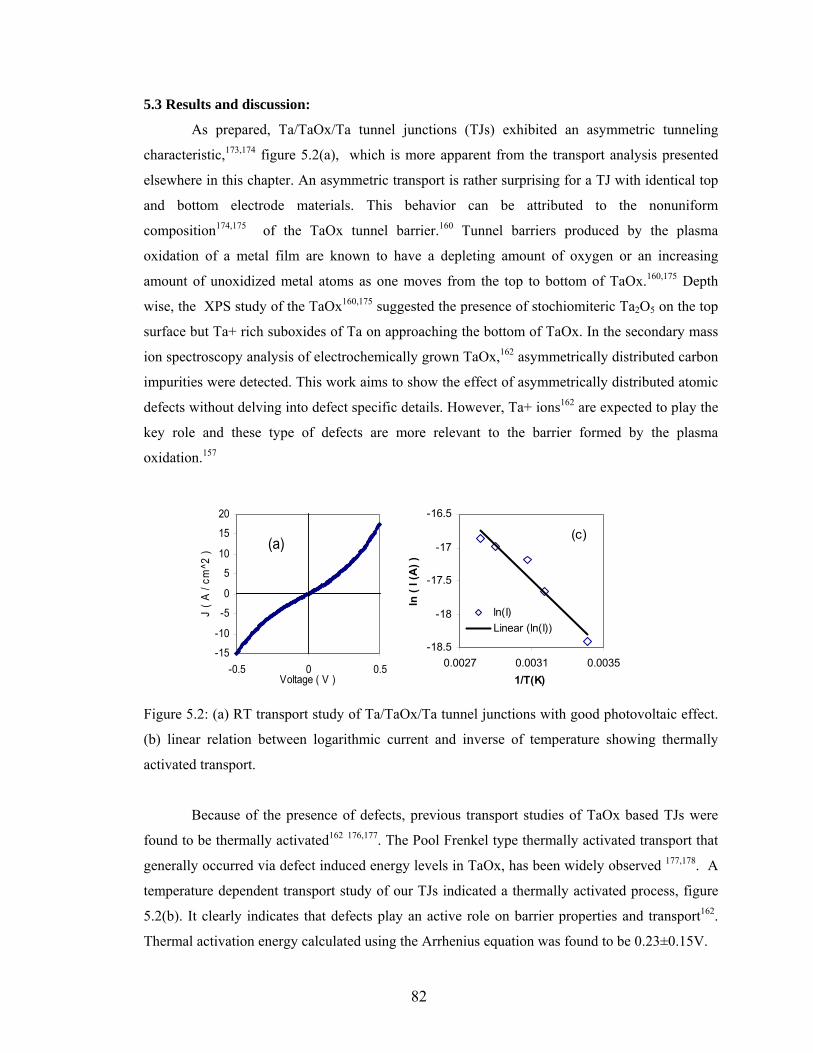
82
5.3 Results and discussion:
As prepared, Ta/TaOx/Ta tunnel junctions (TJs) exhibited an asymmetric tunneling
characteristic,173,174 figure 5.2(a), which is more apparent from the transport analysis presented
elsewhere in this chapter. An asymmetric transport is rather surprising for a TJ with identical top
and bottom electrode materials. This behavior can be attributed to the nonuniform
composition174,175 of the TaOx tunnel barrier.160 Tunnel barriers produced by the plasma
oxidation of a metal film are known to have a depleting amount of oxygen or an increasing
amount of unoxidized metal atoms as one moves from the top to bottom of TaOx.160,175 Depth
wise, the XPS study of the TaOx160,175 suggested the presence of stochiomiteric Ta2O5 on the top
surface but Ta+ rich suboxides of Ta on approaching the bottom of TaOx. In the secondary mass
ion spectroscopy analysis of electrochemically grown TaOx,162 asymmetrically distributed carbon
impurities were detected. This work aims to show the effect of asymmetrically distributed atomic
defects without delving into defect specific details. However, Ta+ ions162 are expected to play the
key role and these type of defects are more relevant to the barrier formed by the plasma
oxidation.157
-15
-10
-5
0
5
10
15
20
-0.5 0 0.5Voltage ( V )
J ( A
/ cm
^2 )
(a)
-18.5
-18
-17.5
-17
-16.5
0.0027 0.0031 0.00351/T(K)
ln (
I (A
) )
ln(I)Linear (ln(I))
(c)
Figure 5.2: (a) RT transport study of Ta/TaOx/Ta tunnel junctions with good photovoltaic effect.
(b) linear relation between logarithmic current and inverse of temperature showing thermally
activated transport.
Because of the presence of defects, previous transport studies of TaOx based TJs were
found to be thermally activated162 176,177. The Pool Frenkel type thermally activated transport that
generally occurred via defect induced energy levels in TaOx, has been widely observed 177,178. A
temperature dependent transport study of our TJs indicated a thermally activated process, figure
5.2(b). It clearly indicates that defects play an active role on barrier properties and transport162.
Thermal activation energy calculated using the Arrhenius equation was found to be 0.23±0.15V.

83
0
40
80
120
160
200
-0.3 -0.15 0 0.15 0.3Voltage(V)
Cap
icita
nce
( p F
)
Dark-10kHzLight-10KHzDark-1MHzLight-1MHz
(c)
Figure 5.3: C-V study of Ta/TaOx/Ta tunnel at 10kHz and 1MHz frequencies in dark and light at
295K.
To further establish the presence of atomic defects within the barrier capacitance-voltage
(C-V), measurements were performed.178,179 The capacitance of TJs was found to vary with
frequency, Figure 5.3. For instance, the capacitance of a typical TJ at 10 kHz (1MHz) was
~140(~38) pF. The capacitance of defect free tunnel junctions are invariant of frequency.180 This
study, although, clearly suggests that TaOx possesses imperfections but does not point to the
position of defects within the barrier.178 To locate the position of defects, we rely on previous
XPS studies on an analogous system.160 It is also noteworthy that for a stoichiometric Ta2O5
capacitor with 3nm thickness and 25μm2 area, calculated capacitance is 3pF. However, in the
present case the capacitance of TaOx is nearly one order higher and can be attributed to the defect
induced states. Defects within the barrier can significantly reduce the effective distance between
two electrodes and can also alter the effective dielectric constant. Furthermore, the capacitance
value of TJ at 10 kHz in dark and white light irradiated TJ are, respectively, 140pF and 180pF.
This study suggests that a TaOx barrier with atomic defects is photoactive as observed in the case
of solar cells.179
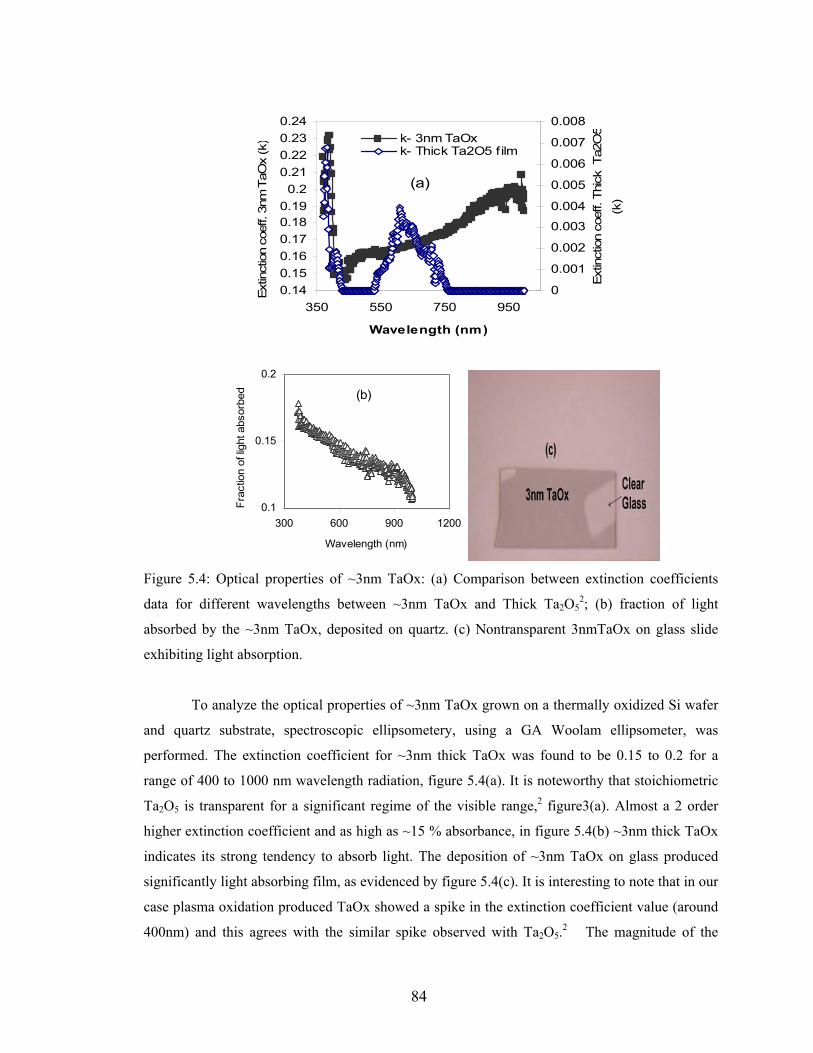
84
0.140.150.160.170.180.190.2
0.210.220.230.24
350 550 750 950
Wavelength (nm)
Extin
ctio
n co
eff.
3nm
TaO
x (k
)
0
0.001
0.002
0.003
0.004
0.005
0.006
0.007
0.008
Extin
ctio
n co
eff.
Thic
k T
a2O
5(k
)
k- 3nm TaOx k- Thick Ta2O5 film
(a)
0.1
0.15
0.2
300 600 900 1200
Wavelength (nm)
Frac
tion
of lig
ht a
bsor
bed (b)
Figure 5.4: Optical properties of ~3nm TaOx: (a) Comparison between extinction coefficients
data for different wavelengths between ~3nm TaOx and Thick Ta2O52; (b) fraction of light
absorbed by the ~3nm TaOx, deposited on quartz. (c) Nontransparent 3nmTaOx on glass slide
exhibiting light absorption.
To analyze the optical properties of ~3nm TaOx grown on a thermally oxidized Si wafer
and quartz substrate, spectroscopic ellipsometery, using a GA Woolam ellipsometer, was
performed. The extinction coefficient for ~3nm thick TaOx was found to be 0.15 to 0.2 for a
range of 400 to 1000 nm wavelength radiation, figure 5.4(a). It is noteworthy that stoichiometric
Ta2O5 is transparent for a significant regime of the visible range,2 figure3(a). Almost a 2 order
higher extinction coefficient and as high as ~15 % absorbance, in figure 5.4(b) ~3nm thick TaOx
indicates its strong tendency to absorb light. The deposition of ~3nm TaOx on glass produced
significantly light absorbing film, as evidenced by figure 5.4(c). It is interesting to note that in our
case plasma oxidation produced TaOx showed a spike in the extinction coefficient value (around
400nm) and this agrees with the similar spike observed with Ta2O5.2 The magnitude of the
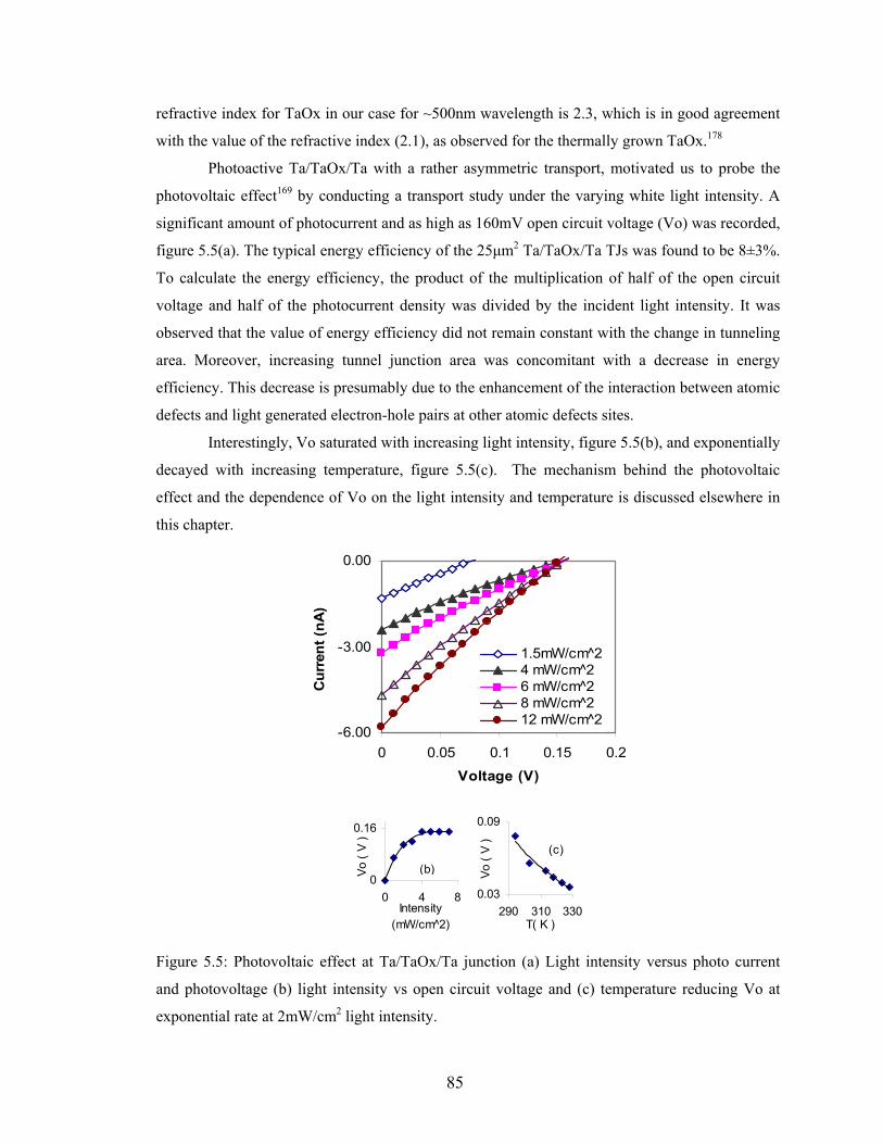
85
refractive index for TaOx in our case for ~500nm wavelength is 2.3, which is in good agreement
with the value of the refractive index (2.1), as observed for the thermally grown TaOx.178
Photoactive Ta/TaOx/Ta with a rather asymmetric transport, motivated us to probe the
photovoltaic effect169 by conducting a transport study under the varying white light intensity. A
significant amount of photocurrent and as high as 160mV open circuit voltage (Vo) was recorded,
figure 5.5(a). The typical energy efficiency of the 25μm2 Ta/TaOx/Ta TJs was found to be 8±3%.
To calculate the energy efficiency, the product of the multiplication of half of the open circuit
voltage and half of the photocurrent density was divided by the incident light intensity. It was
observed that the value of energy efficiency did not remain constant with the change in tunneling
area. Moreover, increasing tunnel junction area was concomitant with a decrease in energy
efficiency. This decrease is presumably due to the enhancement of the interaction between atomic
defects and light generated electron-hole pairs at other atomic defects sites.
Interestingly, Vo saturated with increasing light intensity, figure 5.5(b), and exponentially
decayed with increasing temperature, figure 5.5(c). The mechanism behind the photovoltaic
effect and the dependence of Vo on the light intensity and temperature is discussed elsewhere in
this chapter.
-6.00
-3.00
0.00
0 0.05 0.1 0.15 0.2
Voltage (V)
Cur
rent
(nA
)
1.5mW/cm^24 mW/cm^26 mW/cm^28 mW/cm^212 mW/cm^2
0
0.16
0 4 8Intensity
(mW/cm^2)
Vo (
V )
(b)
0.03
0.09
290 310 330T( K )
Vo (
V )
(c)
Figure 5.5: Photovoltaic effect at Ta/TaOx/Ta junction (a) Light intensity versus photo current
and photovoltage (b) light intensity vs open circuit voltage and (c) temperature reducing Vo at
exponential rate at 2mW/cm2 light intensity.

86
To comprehend the role of atomic defects in rendering tunneling barriers asymmetric and
photoactive, the transport data of as prepared TJs were fitted with Simmons50 and Brinkman
models.173 The rationale behind using the Simmons and Brinkman model is as follows: we
surmise that even though transport between two electrodes is occurring via defects sites, even
then the conduction process between the electrode and an aggregate of defects is governed by the
tunneling mechanism at room temperature. It is noteworthy that the usage of tunneling model in
complex cases109 has given useful insight about conduction mechanism.173 The aim of using
tunneling model here is to understand the Ta/TaOx/Ta tunnel junction qualitatively. The
application of the model on transport data gave effective barrier thickness and barrier height
value, Table 5.1.
Table 5.1: Barrier height and barrier thickness of TaOx tunnel barrier calculated from Simmons
and Brinkman tunneling model.
Model Barrier
Th. (nm)
Barrier
Ht.(V)
Barrier
Asymmetry (V)
Simmons(+Bias/-Bias) 1.5±0.2/1.9±0.15 2.3±0.2/1.5±0.2 0.82±0.2
Brinkman 1.8±0.2 1.5±0.25 1.1±0.3
According to the Simmons model,50 was prepared TJ possessed a thinner (thicker) barrier
and a large (small) barrier height from the top (bottom) electrode side. A stochiometeric TaOx,
i.e. Ta2O5’ should have a uniform value of barrier height throughout. We surmise that the
population of atomic defects, presumably unoxidized Ta (Ta+) atoms, are highest in the
proximity of the bottom electrode and decreases rapidly on approaching the top electrode.160 Such
asymmetric spatial distribution of atomic defects has been concluded to lower the barrier height
near the interface with a higher defect population .177
A previous study suggested that the appearance of the energy levels within the TaOx
barrier were due to the metallic Ta impurities.181 Atomic defects are expected to produce energy
levels starting from the conduction band to the deep level, figure 5.6(c). If this assumption is true,
then defects close to the Fermi level of Ta would allow tunneling via them. This effect will cause
the barrier thickness to be around half of the physical thickness of TaOx. These assumptions are
supported by the barrier thickness values. Effective barrier thickness values obtain by fitting the
transport data with tunneling models fall within the range of 1.5-1.9 nm; TaOx physical barrier
thickness, measured by the ellipsometry, was found to be ~3 nm.176 A smaller barrier thickness is
indicative of defect mediated transport.

87
It has been observed that the values of barrier height and barrier thickness vary with the
range voltage for which transport data is chosen.177 We have fitted the current density data to the
Simmons and Brinkman model to extract barrier thickness using a 1.7 eV experimental value of
the barrier height for the TaOx barrier.182 From both models, barrier thicknesses were found to be
in the range of 1.5-1.9 nm; experimentally measured barrier thickness is ~3nm. It is also
noteworthy that for unrestricted fitting, where barrier thickness and barrier height were used as
variables, barrier height values are in the range of 1.5-2.3 eV, which is in agreement with the
experimentally measured values.182 One surprising thing to note is that the I-V characteristics of a
Ta/TaOx/Ta in our case is quite symmetric in appearance.174 In a few cases, it was found that the
transport analysis of a degraded tunnel junction after heating or intense light exposure produced a
2.5-3 nm barrier thickness and ~0.5 eV barrier height. A smaller barrier height has also been
observed elsewhere.171 The difference in barrier parameters is presumably due to the difference in
the profile and density of atomic defects in a freshly prepared160 and degraded TaOx barrier.
Qualitative mechanism of the photovoltaic effect in Ta/TaOx/Ta is presented in figure 5.6
(a-f). From the XPS studies and discussion thus far it is apparent that a higher density of atomic
defects is present in the vicinity of the bottom electrode, figure 5.6(a). A graded density profile of
donor type defects is expected to transform the ideal tunnel barrier, figure 5.6(b), to produce
asymmetric barrier heights, figure 5.6(c) or a new energy band, figure 5.6(d). Atomic defects far
from the bottom electrode are likely to have different electrostatic environment; and presumably
produce deep-level and photoactive defects.
We conjectured that due to a smaller barrier height photo excited electron from the defect
site in the vicinity of top electrode will move to the bottom electrode.170 While the resulting hole
on the defect level will tunnel towards the top electrode, due to a smaller tunneling distance;
tunneling distance affect the tunneling rate exponentially.50 This mechanism of separating photo-
excited electron hole pairs would enable a net photovoltaic effect. This mechanism bears
resemblance to the Glass model;170 glass model was previously studied to explain the
photovoltaic effects within the oxides due to defect centers.172 Atomic defects, which are closer
to the bottom electrode, will not yield a net photovoltaic effect; holes and electrons from the
defect sites will reach the bottom Ta electrode and will annihilate each other, figure 5.6(e).
Alternative explanation for the photovoltaic effect in this system can be given in the
following manner. Photo-excited electron from the deep level defect, closer to top electrode, will
move to the defect induced energy band. From this band, photo excited electron can move to the
bottom electrode. However, photo-generated hole will more to the top electrode, leading to
charge separation. We have observed that as-prepared TJs open circuit voltage (Vo) saturated

88
once white light intensity increased beyond a threshold point of 4mW/cm2, figure 5.4(b). The
halogen lamp, used in this study, has a wide distribution of wavelengths from infrared to
ultraviolet.183 Photo-generated electron-hole pairs within photoactive regime of tunnel barrier will
be swept to leads causing an accumulation of charges, ultimately defining the Vo. Magnitude of
Vo is a strong function of thickness of depletion layer,183 which is surely complicated to define in
our system160,177 but surely has a finite value which leads to a saturation of Vo. The open circuit
voltage (Vo) was also observed to decrease exponentially with increasing temperature, figure
5.4(c).
To elucidate this observation it is necessary to recall that the transport through as
prepared TJ was found to be thermally activated. The charge flow rate is an exponential
functional of the temperature.162 In other words, accumulated charges, defining Vo on the two
leads are expected to be siphoned out at an exponential rate with increasing temperature.
Therefore a corresponding decrease in Vo, dictated by the accumulated charge, is justifiable.
Figure 5.6: Atomic defect distribution in TaOx barrier (a), ideal tunnel barrier profile (b) large
gradient in atomic defects in TaOx produced asymmetric tunnel barrier and photoactive defect
states within the barrier, shown by dashed line (d). Charge separation is only possible for defect
sites closer to the top electrode, but not for the defects closer to the bottom electrode (e).
The operational life of Ta/TaOx/Ta based thin film solar cell is observed to be strongly
influenced by the heat treatment and exposure time to the intense light radiation. TJ used in this
study started showing instabilities soon after heating above 70 ºC. Long exposure to intense white
light is expected to produce effect similar to the heating; the broad band light source contained

89
radiation in infrared range. When a junction degraded, presumably under the influence of relaxing
tensile stresses, mainly arising from heating, a drastic increase in surface roughness was
observed. In our previous studies, evolution of pinhole population was clearly noticed after the
heating of the cobalt/alumina (2nm) bi-layer system. This event is strongly associated with the
poor facture toughness of insulating film. Due to this reason insulating layer (underlying metallic
layer) fragmented (deformed plastically) under tensile stress, producing pinholes of various
shapes and sizes.184
To verify the role of pinholes, only a bi-layer of Ta/TaOx on Si wafer was studied;
avoiding top layer deposition permits direct observation of morphological changes on a TaOx
layer by the AFM. In the case of the Ta/TaOx system, surface roughness increased 8-10 folds
after a heat treatment at 360 K for 5 min, figure 5.7, which is consistent with the creation of
pinholes on the barrier layer discussed in chapter 2. The TJs affected with pinholes generally
showed a 0.8-1.2V breakdown voltage, and in many cases failed within 2-4 days on their own,
presumably due to the aggravating pinhole effects. Such TJs also exhibited a 0-50mV open
circuit voltage or nil photovoltaic effect.
Figure 5.7: Surface morphology of Ta/TaOx bi layer before (a) and after heating (b) at 360 K for
5min.

90
5.4 Conclusion
In summary, graded density of atomic defects, presumably Ta+, produced an asymmetric
barrier with quantum well type defect levels. Graded density of defects produced net inbuilt
electric field Vo yield a photovoltaic effect on Ta/TaOx/Ta tunnel junctions. These tunnel
junctions showed high vulnerability towards temperature variation and exposure to the intense
light which appeared to produce pinhole type defects causing barrier failure. Ultrathin TaOx
based tunnel junctions are promising candidate for producing economical solar cells. Present
system is likely to be better suited for extracting energy from low intensity radiation. Variety of
substrate can be utilized to produce TaOx based photocells. However, application of such system
would need significant work to improve the stability and reliability. Cheaper thin film solar cells
are feasible with other analogues systems with higher stability. The asymmetric doping of thicker
tunnel barrier may be performed to enhance the photovoltaic effect.
Content of the present chapter also serves as an excellent control experiment for the spin
dependent photo-effect we observed on magnetic molecule treated multilayer edge molecular
electrodes (MEME), details in chapter 7.

91
Chapter 6
Molecular Cluster Induced Antiferromagnetic Coupling between Two Ferromagnetic
Electrodes
6.1 Introduction:
The possibility of producing faster and energy efficient logic and non-volatile memory
devices26 using spin of an electron, spin based devices have attracted enormous interest. Magnetic
tunnel junctions (MTJ) with a multilayer of ferromagnet-insulator-ferromagnet structures are one
of the most promising categories of spin devices.18 Performance of a magnetic tunnel junctions
critically depends upon the magnitude of ferromagnet/insulator interfaces18 possessing complex
electronic properties and dangling bonds.17 Ferromagnet/insulator interfaces are expected to
contribute for ~90% of spin scattering in a spin valve.18 Moreover, reproducible production of
absolutely defect free insulator with angstrom scale precision over thickness, even with a state of
art film deposition system is a daunting task.17 Interestingly, it was found that change in
insulating material in MTJ from alumina to magnesium oxide improved the magneto resistance
ratio from ~50% to 600% with improved interlayer coupling.18
Organic molecules are endowed with small hyperfine splitting and spin orbit coupling as
compared to insulators and semiconductors.26 There is several advantages of using molecules in
spin valve devices. Molecule length can be easily reproduced with an angstrom scale precision
and molecule can be easily functionalized to chemically bond with desired metal.9 These factors
make the molecule a strong contender of conventional insulating materials.20 Previous attempts
for utilizing alkane molecule as an insulator between two Ni ferromagnetic nanowire electrodes
in a nanopore geometry did not demonstrate performance advantages over conventional magnetic
tunnel junctions.16 Devices where molecules are directly sandwiched between two metallic layers
are likely to be affected by impurities,95 mechanical deformations,35 large deviations in transport
characteristics185 and have no intrinsic molecular spin-states as transition metal complexes often
do.
In another study with Ni break junction utilizing C60 molecule, a surprisingly strong
exchange coupling was observed between two Ni electrodes via C60 molecule.13 C60 molecule was
believed to be in low spin state (s=1/2). High spin state molecules,3,33 exhibiting novel transport
phenomenon in a gold break junction based study,33 are expected to produce novel transport
features and magnetic couplings when employed between ferromagnetic electrodes.14 The
magnetic characterization is challenging due to fragility and irreproducibility of molecular

92
devices. 90 Moreover, it is difficult to use ferromagnetic electrodes in present molecular device
designs.
We have recently developed a Multilayer Edge Molecular Electrodes (MEME) for
forming molecular contacts between metal thin films. MEME is essentially an exposed edge
tunnel junction with an insulator thickness close to the dimension of conducting molecular
complexes. Thiol-functionalized metal clusters are bridged between two metal electrodes along
the exposed edges forming molecular electron conduction channels.40 The key advantage is the
freedom to choose virtually any metal as an electrode, including ferromagnetic metals. Molecular
dimension inter-electrode separation is set by the robust insulator,33 which also minimizes the
effect of foreign impurities and works as a diffusion barrier. Importantly, we are able to
characterize the conduction of the device before and after attachment of the molecules, which is a
critical control experiment and accurately measures molecular conduction through the system.
A particularly intriguing hypothesis is whether the spin-state of a molecule can affect the
spin state of the metallic leads. The geometry of the molecule spanning the electrode gap can
allow the exchange of spin specific electrons mediated by well defined molecular electronic states
of transition metals in the clusters. Isolated dots of Ferromagnetic Multilayer Edge Molecular
Electrodes (FMEME) can be magnetically characterized before and after the bridging of high spin
molecular complexes. Here we present the experimental results along with a number of control
studies to demonstrate the effectiveness of high spin state molecule in modifying the magnetic
coupling between two ferromagnetic electrodes of a FMEME. When we used the organometallic
complex3 with (S=6) spin state as a molecular coupler, the magnetic coupling strength between
two electrodes of FMEME increased dramatically to 20 ergs/cm2. The extent of molecule induced
coupling is so strong that signature of original ferromagnetic films vanished at RT even with
applied fields as high as 3 Tesla.

93
6.2 Experimental details:
Figure 6.1: Schematic of fabrication steps for FMEME (a) photolithographically define dot array
in photoresist. (b) Deposition of Ta/Co/NiFe/Al2O3/NiFe multilayer thin film dot, (c) liftoff to
reveal pattern with exposed edges; Ta is seed layer and Co/NiFe layer is magnetically harder than
NiFe. (d) Idealized multilayer electrode dots before and (e) after treatment with molecular
complex. (f) 3D AFM image of a FMEME dot and (g) simplified crystal structure organometallic
molecular complex.3
Approximately 7000 to 21000 FMEME dots were grown on thermally oxidized Si wafers
to attain the detectable signal intensity during magnetization studies. FMEME dots were prepared
by depositing all the films (Ta, Co, NiFe, Al2O3, NiFe) into a single photo resist cavity to form
Ta[5nm]/Co[5nm]/NiFe[5nm]/AlOx[2nm]/NiFe[12nm] samples followed by liftoff to produce
the exposed side edges. Details of photolithography, deposition steps for alumina and top and
electrodes, and molecule attachment have been published elsewhere.40 Each dot was of ~3μm
diameter and dot to dot separation was 3-5μm.

94
Following scheme of molecule attachment was adopted to bridge the molecules on
FMEME dots. A ~2.5nm long organometallic cluster (OMC) with thioacetate terminated tethers
was synthesized3 for attachment across the present electrode design. Through thiol surface
attachment to metal leads, an array of OMC, [(pzTp)FeIII(CN)3]4[NiII(L)]4[O3SCF3]4 [(pzTp) =
tetra(pyrazol-1-yl)borate; L = 1-S(acetyl)tris(pyrazolyl)decane], were covalently linked to top and
bottom electrodes to span the edge of the insulator film to form a dominant conduction
pathway.116 This molecule essentially comprises a cube of 8 edges of cyanide bridged Ni and Fe
atoms (-Ni-N≡C-Fe-). There are four 10 carbon alkane tethers connected to Ni atoms of the
molecule’s cube at one end and to the metal electrode, with thio-acetate group, on another end.3
The thioacetate group is a protecting group to preclude thiol reactions during the formation of an
octametalic core. This thiolacetate group is readily removed during an electrochemical molecule
attachment process117 on the device to form thiol-Ni surface bonds. To attach the molecule to
electrodes, a 2mM solution of OMC in dichloromethane (CH2Cl2) solvent was subjected to the
alternating ±100mV biasing between two metal electrodes with a time interval of 0.02 seconds
for a period of 2 minutes. After the molecule attachment process samples were rinsed with
CH2Cl2, iso-propyl alcohol and DI water (18Mohm), the samples were dried.
We prepared twelve FMEME dot samples with (Ta/Co/NiFe/AlOx(2nm)/NiFe) dots in
different batches. How successful molecule effect is in changing the magnetic coupling between
two FM electrodes of a dot was justified by the FMR study. Twelve FMEME samples were
prepared in this study. Out of twelve samples eight samples were of good quality, while four
samples showed quite erratic magnetic behavior. After the treatment of magnetic molecular
complex3 three samples showed dramatic effects; conventional ferromagnetic film signals
disappearing beyond the detection limit. Out of other four partially successful samples, two
samples showed ~80% decrease in FMR signal intensity while rest of the two samples showed
~25% decrease in FMR signal intensity. Two samples showed negligible effect of molecular
complex. Three samples in bare state itself behaved erratically, presumably due to imperfections
in insulating barrier. Besides the samples of primary composition
(Ta/Co/NiFe/AlOx(2nm)/NiFe), a number of other samples with different film compositions were
prepared to perform control experiments.
It should be noted that our sample fabrication scheme is based on simple
photolithography and thin film depositions. Quality of photoresist, photoresist profile, cleanliness
of liftoff, thickness and quality of ultrathin alumina are of critical importance in producing tunnel
junction dots with exposed side edge and bridgeable insulator thickness. For the sake of
consistency, we have extensively studied the two similar samples, FMEME-A and FMEME-B
95
that showed the strong molecularly induced reorientation of thin film magnetic properties.
FMEME-A and FMEME-B both possessed 14,000 dots.
The magnetization study was performed using the Quantum Design MPMS XL 7T
superconducting quantum interference device (SQUID) magnetometer. The sample was then
mounted on a glass rod with the help of epoxy and introduced into helium gas flushed
superconducting coil of SQUID magnetometer. Samples were centered carefully to get the
optimum signal intensity. The temperature during magnetization study was kept at 150K. Very
low temperature (4K) was observed to damage the tunnel barrier and also made the rotation of
magnetic domains in electrodes film difficult. At higher temperature noisy data were a limiting
factor.
For ferromagnetic resonance (FMR) study Brucker EMX EPR spectrometer equipped
with Brucker Mirowave Bridge ER 041MR and Brucker Power Supply ER 081(90/30) was
utilized. Consistently ~9.7GHz microwave frequency and room temperature was used for all the
experiments. A magnetic field was applied in the sample plane to study the uniform modes of
thin films and multilayers. Application of the magnetic field perpendicular to the sample plane
did not produce a promising distinct signal for the study of molecule effect. Before every sample
cavity’s spectra was checked for the background signal at 5 fold higher gain than that used for the
main samples. FMR spectra of a sample did not change noticeably within the ±10º variation with
respect to the magnetic field direction.
Magnetic force microscope (MFM) studies were performed using Digital instrument’s
multimode AFM. Highly sensitive MFM tips (supplied by Nanosensors) with the following
specifications were utilized: type PPP-MFMR, tip side Cobalt coated, force constant: 0.5-9.5N/m,
resonance frequency 45-115 kHz. During MFM scans the gap between tip and substrate was 10-
150nm. For the high resolution and uninterrupted MFM study 100nm tip sample gap was
maintained.

96
6.3 Results and discussion:
-150
-100
-50
0
50
100
150
-5000 0 5000Field (Oe)
Mom
ent (
µ e
mu)
Bare FMEME-Aw ith OMC
150 K
(a)
0.0E+00
4.0E-05
8.0E-05
1.2E-04
1.6E-04
0 1 2 3Field (Tesla)
Mom
ent (
emu)
(b)FMEME-A
T = 150K
2.1E-05
2.1E-05
2.2E-05
2.2E-05
2.3E-05
2.3E-05
2.4E-05
0 100 200 300 400
Temperature (K)
Mom
ent (
emu)
(c)
T = 150KField =0.5TFMEME-A
0.00
0.05
0.10
0.15
0.20
0.25
0.30
-350 -175 0 175 350
T(K)
1/χ
Intersection point ~330K
After moleculeattachement on FMEME-Aat 0.5T
( d )
Figure 6.2: (a) Magnetization study of FMEME-A dots before and after the attachment of
magnetic molecular complex. Figure (b) is magnetization of the same sample (with molecule) up
to 3T at T=150K. (b) Inverse of magnetic susceptibility vs. temperature curve for the molecule
treated sample used in study (a). (c) Magnetic moment vs. Temperature study on FMEME-A
under 5000 Oe inplane magnetic field.
Magnetization studies were performed to elucidate the effect of molecular complex on
the FMEME dots. A magnetic field was applied in the sample plane and at 150K. FMEME-A
dots exhibited weak antiferromagnetic coupling via ~2nm alumina insulator and exhibited a
saturation magnetization value of ~1.0 × 10⁻⁴ emu at 0.2T. The FMR study, mentioned later in
this dissertation, confirms the nature of coupling to be antiferromagnetic. A little higher coercive
field for magnetic dots, as compared to unpatterned structures (Fe/MgO/Fe), is expected to arise
from the shape anisotropy and inter-dot dipolar interactions.186

97
Within 20 minutes of the molecular bridging on the exposed sides of dots the
magnetization study were performed in the identical conditions as used for the bare sample. After
cluster addition, a dramatic drop (~90%) in the magnetic moment and the appearance of linear
magnetization behavior was observed, figure 6.2(a). Interestingly, magnetic moment of FMEME-
A dots after molecule attachment did not saturate up to 3T magnetic field, figure 6.2(b), and even
slightly surpassed the saturation magnetic moment value for the bare sample at ~0.2 T. A linear
magnetization curve implies that cumulative magnetic response is either paramagnetic or
antiferromagnetic. We surmised that if ferromagnetic electrodes of FMEMEs are
antiferromagnetically coupled via molecular channels then a transition in magnetic moment vs.
temperature study should appear.187 We have plotted the inverse of magnetic susceptibility vs.
temperature to determine the nature and magnitude of coupling via molecule, figure 6.2(d).
Tangent on the part of curve which appear after the transition intersect temperature axis at -
330K187 (Neel temperature); according to Curie-Weiss law this intersection on negative
temperature axis indicates the presence of strong antiferromagnetic coupling associated with the
ensembles of molecule treated FMEMEs.
Another control sample molecule treated FMEME-B, which also showed linear
magnetization vs. magnetic field curve, exhibited -310K Neel temperature; hence showing
consistent behavior with molecule treated FMEME-A. We argue that observed transition and
antiferromagnetic coupling is associated with the molecule induced strong antiferromagnetic
coupling between NiFe and Co/NiFe ferromagnetic electrodes. However, we should address a
plausible experimental concern that the samples could be inadvertently oxidized and render an
antiferromagnetic oxide. Nearly 75% of the ferromagnetic metal on FMEME is NiFe. NiFe is
known to be stable in atmospheric condition until sample is heated beyond 250ºC.114 The possible
antiferromagnetic oxides of NiFe are NiO and FeO possessing 570K and 1000K Neel
temperature, respectively 187. In a typical FMEME, Co is covered by NiFe and only exposed to
the oxidative atmosphere through 5nm thick sides. The ratio of exposed area Co to protected
planar area is ~0.001; cobalt oxide has a 320K Neel temperature187 but cannot dominate the
magnetic property of the whole FMEME stack.
In a control experiment, discussed later in this thesis, a purposefully oxidized FMEME
dot did not markedly change the magnetic response. It is noteworthy that a decrease in magnetic
moment for ~0.2T field (saturation field for the bare sample) is consistent with the
antiferromagnetic alignment of the top and bottom NiFe layers.188 From the saturation values of
separate thin films (Co/NiFe and NiFe) we anticipate that the difference between ferromagnetic
(additive) and antiferromagnetic alignment (subtractive) of the electrodes layers, would afford a ~

98
92±4% change in the magnetization values. The fact that an application of 3T of field did not
switch both ferromagnetic layers to become parallel with the applied field (and reach saturation)
is remarkable. The lower limit energy of coupling is readily estimated by utilizing the volume of
anti-aligned magnetic film, moment (Ma) and applied field(Happl) from the following expression:
appla HMVE ...2= (6.1)
Table 6.1: Calculation of energy and values of parameters utilized in calculation.
Parameters Values
Magnetization of soft film(Ma) 1.2x10⁵ A/m
Thickness of soft film (ta) 1.0x10⁻⁸ m
Applied saturation field (Happ) 3T
FMEME dot diameter 3.0x 10⁻⁶m
Area 7.1x10⁻¹²m2
Volume/dot 2.0x10⁻¹⁹ m3
No. of molecules 1.0x10⁴
Antiferromagnetic coupling energy 1.5x10⁻¹³J or 1.5x10⁻⁶ergs
Energy per unit junction area 21.87 ergs/cm2
Energy per molecule (in Jules) 1.5x10⁻¹⁷ J/molecule
Energy per molecule (in eV) 97.0 eV
It was seen that the energy/dot is on the order of micro-ergs which translates to ~20
ergs/cm2 , when using the planar area of the electrode. This is an unprecedented value compared
to the previously large value of ~0.8erg/cm2 coupling energy between two ferromagnetic
electrodes with impurity assisted defects.95 In our case, strongly coupled molecules play the role
of well defined and controllable impurities. If we use a more stringent coupling area of just the
electrode edge where the molecules are (10um x 1nm) the coupling energy becomes a dramatic
16,000 erg/cm2 corresponding to 97eV per molecule. Clearly at these unreasonable energies, the
coupling must be distributed over a large number of ferromagnetic atoms. The following chapter
discusses the high degree of spin polarization in the metallic leads and the role of molecular spin-
state in electron conduction/filtering.

99
The value of 20ergs/cm2 is also consistent with extrapolation from observed shifts in
spin-flipping in the literature. According to an experimental study,186 nearly 50 Oe shift in
magnetization loop of soft magnetic layer of a tunnel junction corresponded to ~0.25erg/cm2.
Linear relation between shift in saturation field and antiferromagnetic coupling of a MTJ suggests
that for a 3T shift in saturation field antiferromagnetic coupling has to be 30erg/cm.2 In another
study, a magnetic ferromagnet/nonmagnet/ferromagnet system with 1.54erg/cm2
antiferromagnetic coupling was calculated to saturate ~0.5 T.189 Assuming a linear relation
between coupling energy and saturation field and nominal effect of film thickness, we find that
lower bound of molecule induced antiferromagnetic coupling strength is ~9 erg/cm2. It is worth
noting that molecule induced coupling is nearly 1-2 orders higher than the maximum
antiferromagnetic exchange coupling seen with ~0.5 nm thick MgO insulator.186 Bare FMEME,
with 2nm thick barrier, is expected to have coupling energy several orders smaller than 1x10⁻³
erg/cm,2 energy for the 0.8nm thick insulator.95
For most hard/soft thin film systems, the B-H response shows a sharp transition as the
soft layer flips as diagrammed in figure 6.4. Coupling typically shifts this to a higher field. In
our system we don’t see a flat response with sharp transition, but we observe a shallow linear
slope. Linear magnetization curves for the system of two ferromagnetic electrodes with
antiferromagnetic coupling is feasible when antiferromagnetic coupling strength (J) is
significantly greater than the product of the anisotropy constant (K) and film thickness (t) for
ferromagnetic films189: J>K*t.189 K is typically ~105 erg/cm3 for Ni and Fe.187 Assuming a film
thickness of 20 nm, we get K*t = ~0.2erg/cm2 far below the estimated 20 erg/cm.2 A linear B-H
response is seen in figure 6.2(b).
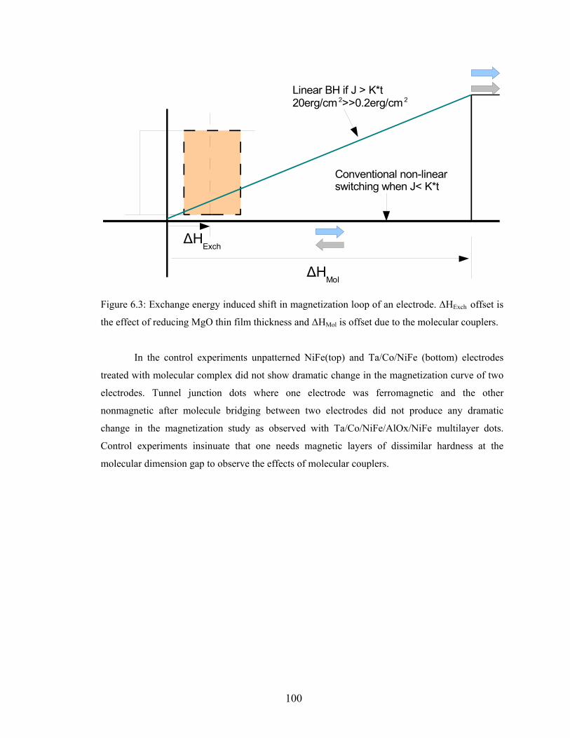
100
ΔHExch
ΔHMol
Linear BH if J > K*t20erg/cm 2>>0.2erg/cm 2
Conventional non-linear switching when J< K*t
Figure 6.3: Exchange energy induced shift in magnetization loop of an electrode. ΔHExch offset is
the effect of reducing MgO thin film thickness and ΔHMol is offset due to the molecular couplers.
In the control experiments unpatterned NiFe(top) and Ta/Co/NiFe (bottom) electrodes
treated with molecular complex did not show dramatic change in the magnetization curve of two
electrodes. Tunnel junction dots where one electrode was ferromagnetic and the other
nonmagnetic after molecule bridging between two electrodes did not produce any dramatic
change in the magnetization study as observed with Ta/Co/NiFe/AlOx/NiFe multilayer dots.
Control experiments insinuate that one needs magnetic layers of dissimilar hardness at the
molecular dimension gap to observe the effects of molecular couplers.

101
-100000-80000-60000-40000-20000
020000400006000080000
100000
0 2000 4000
Field(Oe)
Inte
nsity
(a.u
)
Bare FMEME-BWith OMC
(a)
FMEME-B
05
10152025303540
Before After
Thic
knes
s( n
m )
( b )
-60000
-40000
-20000
0
20000
40000
60000
400 900 1400Field (Oe)
Itens
ity (a
.u.)
Fresh NiFe
Oxidized
(c)
-40000
-30000
-20000
-10000
0
10000
20000
30000
400 900 1400
Field (Oe)
Inte
nsity
(a.u
.)
Bare FMEME[4nm AlOx]w ith OMC
( d )
-80000
-60000
-40000
-20000
0
20000
40000
60000
400 900 1400Field ( Oe )
Inte
nsity
(a.u
.)
Bare FMEME (2nm)w ith C20 Mol
(e)
-60000
-40000
-20000
0
20000
40000
60000
80000
400 900 1400
Field (oe)
Inte
nsity
(a.u
)
NiFe-AlOx2nm-NiFew ith OMC
( f )
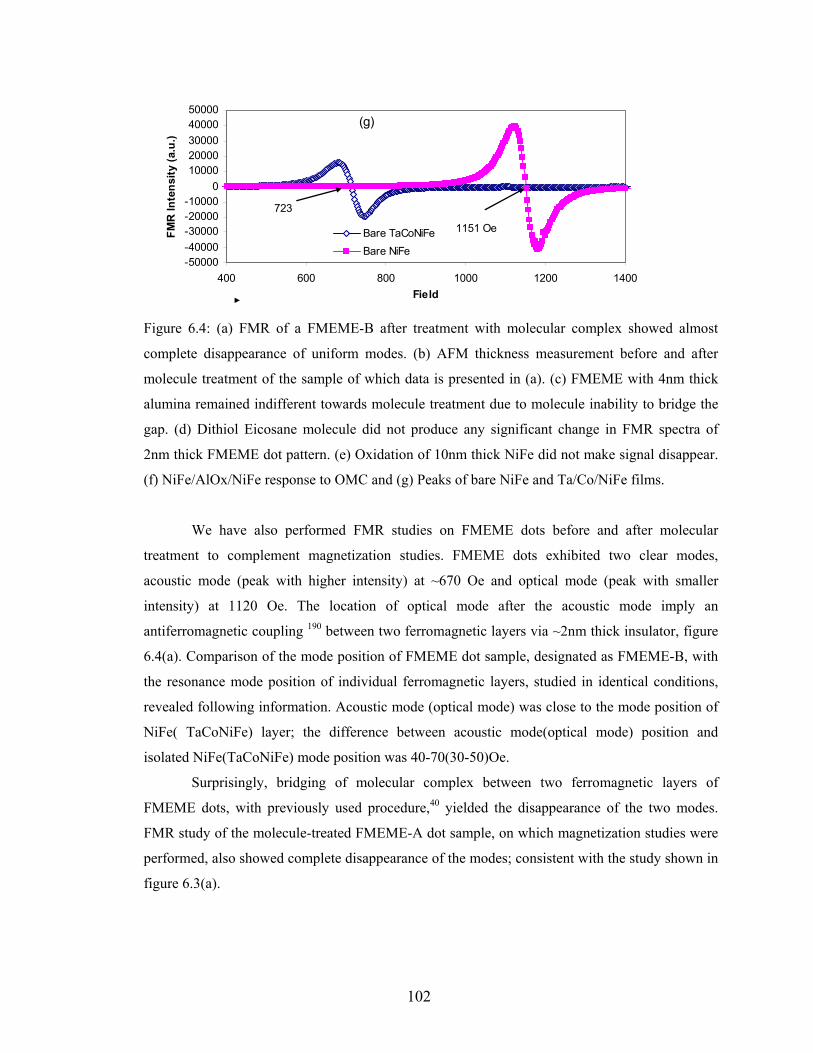
102
-50000-40000-30000-20000-10000
01000020000300004000050000
400 600 800 1000 1200 1400Field
FMR
Inte
nsity
(a.u
.)
Bare TaCoNiFeBare NiFe
(g)
723
1151 Oe
Figure 6.4: (a) FMR of a FMEME-B after treatment with molecular complex showed almost
complete disappearance of uniform modes. (b) AFM thickness measurement before and after
molecule treatment of the sample of which data is presented in (a). (c) FMEME with 4nm thick
alumina remained indifferent towards molecule treatment due to molecule inability to bridge the
gap. (d) Dithiol Eicosane molecule did not produce any significant change in FMR spectra of
2nm thick FMEME dot pattern. (e) Oxidation of 10nm thick NiFe did not make signal disappear.
(f) NiFe/AlOx/NiFe response to OMC and (g) Peaks of bare NiFe and Ta/Co/NiFe films.
We have also performed FMR studies on FMEME dots before and after molecular
treatment to complement magnetization studies. FMEME dots exhibited two clear modes,
acoustic mode (peak with higher intensity) at ~670 Oe and optical mode (peak with smaller
intensity) at 1120 Oe. The location of optical mode after the acoustic mode imply an
antiferromagnetic coupling 190 between two ferromagnetic layers via ~2nm thick insulator, figure
6.4(a). Comparison of the mode position of FMEME dot sample, designated as FMEME-B, with
the resonance mode position of individual ferromagnetic layers, studied in identical conditions,
revealed following information. Acoustic mode (optical mode) was close to the mode position of
NiFe( TaCoNiFe) layer; the difference between acoustic mode(optical mode) position and
isolated NiFe(TaCoNiFe) mode position was 40-70(30-50)Oe.
Surprisingly, bridging of molecular complex between two ferromagnetic layers of
FMEME dots, with previously used procedure,40 yielded the disappearance of the two modes.
FMR study of the molecule-treated FMEME-A dot sample, on which magnetization studies were
performed, also showed complete disappearance of the modes; consistent with the study shown in
figure 6.3(a).

103
Theoretically, it was calculated that such mode disappearance is only possible when
antiferromagnetic coupling strength between two ferromagnetic layers cross a critical limit; in
this case spin flip occurs. Two ferromagnetic layers in such case behave like one unless the
applied magnetic field is of the order of strong antiferromagnetic coupling energy.191 To make
sure that severe damage to the sample (i.e. complete etching of magnetic dots) is not the reason
for the FMR signal disappearance, the thickness of dots were monitored before and after
molecular treatment. Thickness measurement by the AFM showed unnoticeable statistical
difference in the heights of dots. More than 140 dots at near corners and in the central parts were
studied to give the statistical heights distribution before and after molecule attachment figure
6.4(b). The similar thickness of FMEME dots before and after molecule treatment insinuates that
both etching and significant oxidation (volume expansion) did not occur. High magnification
optical microscopy with polarized light could be used for the confirmation of sample integrity.
SEM and AFM were also performed on selected samples in agreement with optical microscopy.
In some cases a small population of dots (5-10%) underwent partial to complete damage during
electrochemical treatment. Electrochemical damage is the topic of appendix A2 of this thesis.
FMR study of such samples did not exhibit more than 10% change in signal intensity due to
molecule treatment that induced observable damage.
To check the possibility that unnoticed oxidation of dots produced antiferromagnetic
oxides, e.g. NiO and FeO, thus leading to the disappearance of FMR modes NiFe ferromagnetic
electrode were purposefully plasma oxidized to revealed the distinct and expected mode of bulk
ferromagnet. Hence surface oxides can not be the reason for the FMR mode disappearance. After
plasma oxidation of NiFe and additional resonance peak at 800 Oe, figure 6.4(c). We attribute
this addition peak to the oxidized NiFe enabling near surface NiFe to behave differently than the
intact NiFe.
Central to the primary hypothesis is that the molecule spanning the electrode gap is
responsible for the coupling between layers. The molecules simply residing on the surface (not
spanning between two films) would not induce coupling. Individual ferromagnetic layer, as used
in a typical FMEME dot, were given the same molecular treatment from the same molecular
solution, as used for the FMEME dots. The FMR study showed no shift in mode position or any
dramatic reduction in the mode intensity after molecular treatment. A number of other control
experiments were performed to validate our hypothesis that only magnetic molecular bridges on
the exposed edges of FMEME dots are producing extremely strong antiferromagnetic coupling. If
the insulator layer thickness of FMEME dots is more than the molecule length, then the molecule
can not bridge the gap and hence no change in FMR signal due to molecule treatment will result.

104
We indeed observed that FMEME dots prepared with 4nm thick alumina barrier did not show any
significant change in FMR signal after magnetic molecule treatment, figure 6.4(d). A smaller
overlap of two modes of FMEME dots with 4nm thick barrier confirms that we indeed used a
thicker barrier in this study; the thinner the barrier, the more the overlap. To answer this question
we bridged the dithiol-eicosane molecule a 20 carbon alkane molecule without transition metal
core) on the FMEME dots with ~2nm alumina thickness. FMR signal did not show noticeable
change due to alkane molecule treatment, figure 6.4(e).
Another test of the hypothesis is to change the composition of the electrode metal to be
dimagnetic or symmetric soft ferromagnetics. NiFe/AlOx/Au and NiFe/Al2O3/NiFe were studied
before and after magnetic molecule treatment. No dramatic change in FMR signal was observed
after the attachment of the molecular complex to bridge the two metals. In the case of
diamagnetic gold antiferromagnetic coupling is not possible and the ferromagnetic layer behaves
normally. In the case of NiFe/AlOx(2nm)/NiFe, shown in figure 6.4(e), no dominate hard layer is
present (i.e. Co) to initiate ordering. Due to the similar magnetic properties of the NiFe layers,
two modes of bare sample are not very distinct as is in the Co/NiFe/Al2O3/NiFe samples.
From the experimental efforts presented thus far we conclude that strong
antiferromagnetic coupling is specific to the magnetic molecular complex (organometallic
complex) and FMEME dots with Co/NiFe and NiFe ferromagnetic electrodes. Magnetic moment
per atom for Co(5nm)/NiFe(5nm) and NiFe 10nm are ~1.95µB and ~2.2µB ,respectively.192
Moreover, magnetic properties of NiFe in Co/NiFe are strongly influenced by the Co seed
layer193. Our FMR study shows the resonance mode at different mode positions for the each
electrodes material.

105
Figure 6.5: Topography (a) and magnetic image (b) of bare FMEME-B. Same sample after the
treatment with molecular complex show clear topography (c) but disappearance of magnetic
contrast on the majority of the dot positions (d).
Magnetic Force Microscopy can also confirm the spatial location of magnetic moments.
Magnetic imaging of FMEME dots were carried with AFM. MFM study presented here is on
FMEME-B sample; sample on which FMR study, shown in figure 3(a), before and after molecule
attachment was performed. Before molecule attachment FMEME-B dots exhibited unambiguous
magnetic images, figure 6.5(b), corresponding to their physical location and dimensions, figure
6.5(a).
After magnetic molecule attachment, most of the dots showed nil to negligible contrast in
the magnetic images, figure 6.5(d), consistent with B-H, FMR data of antiferromagnetism. The
topography data of the MFM also demonstrated that the dots were not chemically
etched/damaged or oxidized. Separation between a Co coated MFM cantilever and the sample
was 100nm for both imaging. Fresh MFM cantilever were utilized to avoid the loss of the
magnetic signal due to abraded magnetic layer on old tips. The very same MFM cantilever,
showing loss of magnetic signal on molecule treated FMEME dots, showed clear magnetic
images of identical bare FMEME dot sample in the identical experimental condition, thus is not a
(a) (b)
(c) (d)

106
measurement artifact. The fact that we could image a single dot in figure 6.5(d) also demonstrates
that MFM was properly tuned for the null result of the other 14 dots in the image frame. Loss of
magnetic contrast was observed on ~90% the dots studied by the MFM.
-80000-60000-40000-20000
020000400006000080000
100000
0 500 1000 1500 2000Field (Oe)
Inte
nsity
(a.u
.)
Bare FMEME*FMEME-A before molecule burningFMEME-A after molecule burning
( a )
-80000
-60000
-40000
-20000
0
20000
40000
60000
80000
0 500 1000 1500 2000Field (Oe)
Inte
nsity
(a.u
.)
Bare FMEME-BBefore HeatingAfter heating
(b)
Figure 6.6: (a) FMR spectra of the FMEME-A sample before and after burning of molecules in
oxygen plasma, this is the sample on which magnetization studies were performed. FMR of bare
state FMR data is from different sample with identical multilayer configuration. (b) FMR spectra
of the FMEME-B sample before and after heating to 390K. Note this is the sample on which
FMR study showed mode disappearance after molecule attachment.

107
A ferromagnetic metal posses both majority and minority spin density of states; loss of
magnetic contrast at FMEME dot sites at RT indicates evolution of spin bands under the effect of
strong magnetic molecular coupling. Two ferromagnetic layers appear to have a significantly
higher difference in density of states for the spin up and spin down electrons than 42(45)% for
Co(Ni or Fe).17
Figure 6.7: (a) Topography and (b) magnetic image of FMEME-A dot sample after the plasma
oxidation of previously AF coupled array. (c) Topography and (d) magnetic image of molecule
complex treated FMEME-B after heating to damage the dot’s tunnel barrier.
A critical control experiment is to show the reversibility of the strong AF ordering. This
would demonstrate that the observations of small magnetic signal are not due to sample damage.
Two kinds of reversible experiments were performed. In the first reversible approach, molecular
bridges were burnt in the oxygen plasma (50W, 60mTorr mixture of 1:1 Ar:O2 mixture). For this
study the same sample FMEME-A on which magnetization and FMR study exhibited dramatic
change, was utilized. FMR study after plasma treatment showed the reappearance of
unambiguous FMR modes in the spectra, hence proving that the molecule effect is indeed
reversible. Importantly, position and shape of the two modes are in agreement with the acoustic
and optical modes of a bare FMEME sample, figure 6.6(a). It should be mentioned that we did
not perform the FMR study on FMEME-A sample before molecule attachment since it was the
object of B-H studies.
(a) (b)
(c) (d)

108
We also performed a MFM study and observed clear magnetic images, figure 6.7(b), that
commensurate with the topography, figure 6.7(a), of corresponding dots. Thus the ferromagnetic
response of the multilayers was restored after the removal of the coupling organometallic
complexes. We did observed partial damage to the dots after plasma treatment, mainly near
edges of the dots. We attribute these damages to the stress induced flaying of dot material due to
the volume expansion inherent with oxidation. This experiment also provides strong support to
our argument that the accidental oxidation of the sample at any stage can not make the magnetic
mode disappear in FMR study. Oxidation is a diffusive process and will be restricted to surfaces
of the dot. Most of the ferromagnetic material is not oxidized and observed in the FMR study,
figure 6.6.
Another method to demonstrate the reversibility of the strong AF coupling is to damage
the insulating barrier of FMEME dots to allow competing magnetic coupling via high density
pinholes and defects186 or simply short circuit any spin polarization. We have observed that
heating induced tensile stresses fragments the ultra-thin alumina layer.194
For this study we chose the same sample on which FMR modes magnetic image contrast
previously disappeared after the treatment with magnetic molecular complex, sample FMEME-B.
The sample was heated at 390K for 30min in flowing helium ambience, to avoid unintentional
oxidation. The sample was cooled to room temperature and was subjected to FMR study. FMR
spectra of this sample showed clear broad resonance mode; start and end point of mode position
is within the combined range of mode positions for the two ferromagnetic layers. We attribute the
broadened resonance mode to the emergence of wide range of coupling strength between two
ferromagnetic electrodes via defective insulator.190 The MFM study, figure 6(d-e), showed that
FMEME-B sample possessed a sizeable number of dots showing clear magnetic contrast
(ferromagnetic). However, large number of dots still showed negligible magnetic contrast
(antiferromagnetic) and can be attributed to the significant number of dot insulator barriers
surviving the heat treatment.
The ~4 orders increase in magnitude of antiferromagnetic coupling between two
ferromagnetic electrodes induced by the transition metal complex is dramatic and unprecedented.
When accounting for the small area of molecular contacts, the coupling is many orders of
magnitude above previous experimental observation and theoretical prediction. Certainly this
report is based on the previously described experimental observations and careful control
experiments; however, there is significant importance to discussing the mechanisms of molecular
coupling and the plausibility of this remarkable observation. From our previous study of the
MEME using the same organometallic molecular cluster (OMC) we found that the conduction

109
mechanism was primarily 1) tunneling from metal electrode to oranometalic core by tunneling
through alkane tether that acts as a tunnel barrier 2) rapid electron transfer within the
organometallic Ni-CN-Fe cube and 3) tunneling through alkane tether to the other electrode.
Well defined spin-states in the organometallic Ni-CN-Fe cube would determine electron spin-
conduction and possibly provide a mechanism for coupling. A relatively small number of
molecules at the edge of the junction can affect a large volume of ferromagnetic metal atoms.
Apart from experimental evidence, theoretical study46 also supports the evolution of
strong influence of molecular channels on our tunnel junction with 7μm2. Theoretical study
treating transport via tunneling barrier and atomic impurity on equal footing revealed the
following information. A single atomic impurity at 0.75nm distance from the metal electrodes of
a 1.5nm thick barrier could dramatically change the spin polarized transport in a magnetic tunnel
junction of 0.01μm2 planar area. Extrapolating this result for 10μm2 junction area, one would
need 10,000 atomic impurities in the center plane of the tunnel barrier; it is a difficult task to
control the position of atomic defects for any useful application.
Assuming our molecule plays the role of an atomic impurity, we find that the ~10,000
molecules we are attaching via alkane tethers is a sufficient number, in the light of theoretical
calculation, for the 10μm2 junction area. A molecular core, ~0.7nm wide, is 1.2 nm away from the
metallic electrode; a similar gap was used in the theoretical calculation. It is noteworthy that
unlike impurities we are able to control the position, i.e. around the center of the insulating
barrier, of the molecular core with the help of alkane tethers. Alkane tethers possess smaller
barrier height than that of alumina barrier; charge exchange via molecular channels is expected to
be significantly better than alumina or any other inorganic insulating barrier. Since our molecules
are placed outside the tunneling barrier, we have the distinct advantage of comparing the effect of
molecules with that of a good quality tunnel barrier. Exchange coupling of magnetic tunnel
junction is effectively described by the Slonczewski’s model, with following expression.186
dkB ekkkkd
kkkkkkkkJ .2
22222222
223
)()()())(( −
↓↑
↑↓↓↓↓↑
+++−−
=π
ϕ (6.2)
Here, d and φB are the barrier thickness and barrier height, respectively, of the insulating medium
between two spin polarized electrodes, whereas, k↓ and k↑, are the wave vectors of the spin down
and spin up electrons of the ferromagnetic layers. The wave vector of an electron in the insulating
regime is k and is given by a relation, k=√(2.φB.m.ћ-2 ). Here, m is the effective mass of the
electron and ћ is Planck’s constant.
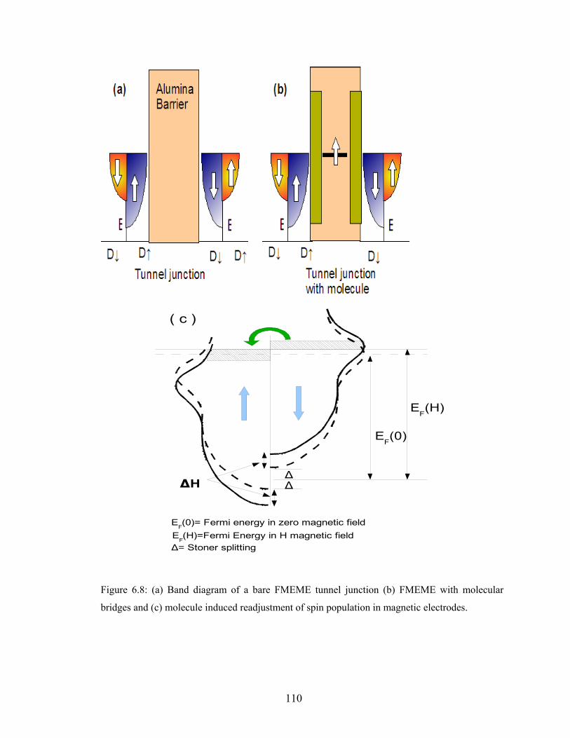
110
ΔΔ
EF(0)
EF(H)
ΔH
EF(H)=Fermi Energy in H magnetic field
EF(0)= Fermi energy in zero magnetic field
Δ= Stoner splitting
( c )
Figure 6.8: (a) Band diagram of a bare FMEME tunnel junction (b) FMEME with molecular
bridges and (c) molecule induced readjustment of spin population in magnetic electrodes.

111
We assume that molecular complex, which has net spin state, behaves like a spin
polarized electrode and hence reduces the effective barrier thickness from 2nm to 1nm(distance
between center of the molecule core to the metal electrode edge). From eqn1, exchange coupling
expression can be simplified to J~(1/d2).exp(-2k.d).186 Assuming the barrier height of 1eV, it is
easy to see reduction in barrier thickness from 2nm to 1nm produces 5 orders stronger exchange
coupling strength. Moreover, the coupling energy between two metal electrodes changes
monotonically with thickness.186 This simple calculation can be applied to exchange coupling
due to atomic defects within tunnel barrier.95 It was found that an impurity level present around
the center of tunnel barrier and providing local density of states close to the metal electrode’s
Fermi level increased coupling strength by up to ~3 orders.95 It is worth noticing that in our case,
molecules also provide local density of states around the center of the tunnel barrier as confirmed
by the molecular transport study for the same molecular complex in the MEME geometry.40
There are few major points to justify why the molecular complex in the present case
produce an extremely strong antiferromagnetic exchange coupling. It is well established that
molecular levels overlap with a continuum of metallic levels to undergo broadening;55 broadening
significantly increase the charge transport rate to and from the molecular levels.35 Increased
probability of exchange of charge via molecular channels is expected to significantly enhance the
superexhange type interaction between ferromagnetic electrodes via molecule.49
It is worth noting that if molecule possess non-degenerate energy levels for the spin up
and spin down electrons then, in addition to enhancing the magnetic coupling molecule can also
serve as a spin filter between two spin reservoirs.195 How a molecule is bonded to the metal
electrode can dramatically effects the molecular transport and exotic phenomena.35 It was found
that the cobalt phthalocyanine (CoPc) molecule exhibited ~ 200 K Kondo temperatures when
molecule interaction to the Au electrode was changed from physiosorption to covalent type.
Moreover, alkane tethers used in our case to covalently bridge the molecule to the metal
electrodes are much more effective electron channels than the vacuum gap37 and a barrier height
of only 0.8eV seen.
Exchange coupling via molecule can be tremendous if the spin state of a molecule
interacts with the ferromagnetic electrodes. Physio-sorbed C60 molecule, in s =1/2 spin state,
produced unprecedented coupling strength between two magnetically asymmetric Ni electrodes
of a break junction.13 The strong exchange coupling via molecule was believed to produce ~70T
magnetic field in the vicinity of molecular junction. Under the influence of this strong magnetic
field, the molecular level produced ~16mV Zeeman splitting.13 The extent of splitting was
proportional to the product of molecule coupling energy with electrodes and spin polarization of

112
the ferromagnetic electrode. It is worth noticing that huge Kondo splitting at cryogenic
temperatures was observed due to one C60 molecule and more importantly with microscopic Ni
electrodes.13 The molecule mediated inter-electrode coupling is only expected to be a local effect
and which can affect the molecular levels to manifest unprecedented Kondo splitting. Here we
argue that in our case we have utilized two ferromagnetic electrodes having the effective area
comparable with that reported by Pasupathi et al13. In the previous study, ferromagnetic
electrodes were made of different hardness using shape anisotropy effect, but in our case we used
different compositions. In the present study, the major difference with regards to the work of
Pasuppathi et al., is that we covalently (not physio-sorption) attached ~10,000 high spin state
magnetic molecular complex; a much stronger effect than that of a single molecule is expected.97
Moreover, spin transport to and from the molecular complex is to occur via organic alkane
molecule dominant spin channels; organic molecules are well known to be more efficient spin
channels than other conventional insulators and semiconductors.27 We are not aware of the exact
spin state of our molecule when bridged between two metal electrodes. Our molecular complex
exhibited S=6 spin state at 10K and S=3 spin state at 77K in the bulk form.3 We surmise that after
attaching the molecule to two ferromagnetic leads; it will possess a spin state of more than one.
In particular, the process of conducting spin selective molecules through a cluster would likely
induce spin ordering with the ferromagnetic electrodes. It is noteworthy that molecular charge
state that could not be stabilized in free molecules was observed in the vicinity of metallic
electrodes.39 For instance s=1/2 spin state of the vanadium complex, was only observed after
placing them between two gold metal electrodes.39
Our magnetic studies, especially MFM, strongly suggest a significant change in the
density of states of the spins in two ferromagnetic layers. We surmise that molecule induced
exchange coupling produced a strong magnetic field that not only split the molecular levels but
also acted upon ferromagnetic atoms attached to them or in close proximity. This can induce
Zeeman splitting to enhance the splitting between spin up and spin down electron density. This
effect in turn can produce a difference in chemical potential under the effect of magnetic field.
Spin dependent exchange coupling via molecule is shown to produce an effective magnetic
field.13 In the context of our multi-molecular system where two ferromagnetic electrodes are anti-
parallel to each other, for the exchange induced magnetic field (B), the following form can be
utilized.13
113
B
N
nnBBnTT
g
PPaB
μ.
)(1∑=
Γ−Γ≈ (6.3)
Here, N is the total number of molecules bridging the gap between ferromagnetic layers, PT(PB) is
the degree of spin polarization of the top (bottom) ferromagnetic layer, and ΓnT (ΓnB) is the
coupling energy of the nth molecule with the top (bottom) layer. g and μB denote the
gyromagnetic ratio for the molecule and Bohr magnetron, respectively.
In order to estimate the magnitude of B, we can consider N=10,000, aP is 0.1592 and gμB
~115μV/T.31 Generally molecular coupling energy is ~10 meV.13 Assuming a conservative range
for the difference in coupling energy is 0.001-0.01 mV, for this we obtain B in the range of ~100-
1000T. In a previous study,13 the effect of extremely high molecule induced exchange field was
clearly observed in the form of unprecedented Kondo level splitting. We surmise that same
field/splitting energy also acts on ferromagnetic electrodes in the vicinity of molecular junctions.
This produces strong Zeeman splitting which in turn will produce readjustment of spin density of
states according to the molecule induced equilibrium. Here we wish to mention explicitly that
magnetic field arising from molecule-mediated interlayer exchange coupling is only a local field.
We are unable to explain how this local field can affect the spin polarization or stoner splitting of
a microscopic magnetic electrode.
In the MFM study, we had an unambiguous signature of dramatic change in spin
polarization at individual electrodes due to molecular complexes. We believe that the evolution of
highly spin polarized magnetic layers is primarily due to the large Zeeman splitting energy
produced by the molecular complexes. According to the calculation of Slonczewski94, the degree
of spin polarization of tunneling electrons depends on the height of the tunneling barrier. With the
higher barrier, one recovers the classical expression of spin polarization; but for the small barrier
height, spin polarization can be dramatically different.17,94 A discussion on spin polarization of
bare and molecule treated FMEME is furnished in chapter 7.
6.4 Conclusion:
We have found that magnetic molecular channels bridged over the insulator gap on
exposed sides of a magnetic tunnel junction strongly influenced the coupling strength between
two ferromagnetic electrodes of the host tunnel junction. Dramatic antiferromagnetic coupling
energies of at least 20ergs/cm2 are seen using the entire planar junction area (7um2). If only the
molecular junction area is considered, then the coupling can be 3-orders of magnitude higher.
The process is reversible with the removal of molecular coupling and only hard/soft

114
ferromagnetic electrode systems work. The phenomenon is seen by B-H, FMR and MFM
studies. Recent theoretical studies, predicting the strongly correlated states between molecule and
ferromagnetic leads97, and utilizing variational spin density of state of ferromagnetic electrodes
strongly coupled to quantum dot, can represent our system.99 However, the unprecedented
magnitude of the coupling (especially if one considers only the molecular junction area) many
atoms must be involved with the coupling and the conduction electrons may be an important part
of the coupling mechanisms. Molecular spin devices formed by bridging of high spin molecule,
with well defined atomic orbitals, on the sides of a magnetic tunnel junction are expected to show
dramatic change in spin dependent transport and would likely be the source of or a product of the
observed dramatic magnetic coupling.
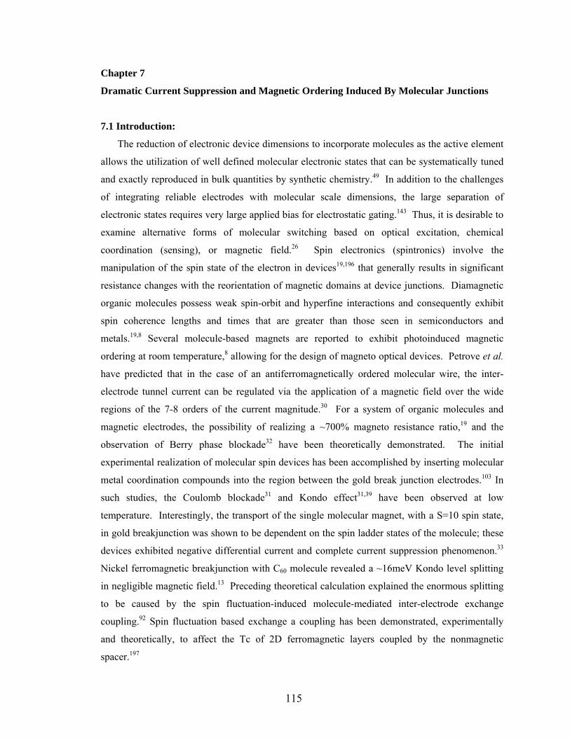
115
Chapter 7
Dramatic Current Suppression and Magnetic Ordering Induced By Molecular Junctions
7.1 Introduction:
The reduction of electronic device dimensions to incorporate molecules as the active element
allows the utilization of well defined molecular electronic states that can be systematically tuned
and exactly reproduced in bulk quantities by synthetic chemistry.49 In addition to the challenges
of integrating reliable electrodes with molecular scale dimensions, the large separation of
electronic states requires very large applied bias for electrostatic gating.143 Thus, it is desirable to
examine alternative forms of molecular switching based on optical excitation, chemical
coordination (sensing), or magnetic field.26 Spin electronics (spintronics) involve the
manipulation of the spin state of the electron in devices19,196 that generally results in significant
resistance changes with the reorientation of magnetic domains at device junctions. Diamagnetic
organic molecules possess weak spin-orbit and hyperfine interactions and consequently exhibit
spin coherence lengths and times that are greater than those seen in semiconductors and
metals.19,8 Several molecule-based magnets are reported to exhibit photoinduced magnetic
ordering at room temperature,8 allowing for the design of magneto optical devices. Petrove et al.
have predicted that in the case of an antiferromagnetically ordered molecular wire, the inter-
electrode tunnel current can be regulated via the application of a magnetic field over the wide
regions of the 7-8 orders of the current magnitude.30 For a system of organic molecules and
magnetic electrodes, the possibility of realizing a ~700% magneto resistance ratio,19 and the
observation of Berry phase blockade32 have been theoretically demonstrated. The initial
experimental realization of molecular spin devices has been accomplished by inserting molecular
metal coordination compounds into the region between the gold break junction electrodes.103 In
such studies, the Coulomb blockade31 and Kondo effect31,39 have been observed at low
temperature. Interestingly, the transport of the single molecular magnet, with a S=10 spin state,
in gold breakjunction was shown to be dependent on the spin ladder states of the molecule; these
devices exhibited negative differential current and complete current suppression phenomenon.33
Nickel ferromagnetic breakjunction with C60 molecule revealed a ~16meV Kondo level splitting
in negligible magnetic field.13 Preceding theoretical calculation explained the enormous splitting
to be caused by the spin fluctuation-induced molecule-mediated inter-electrode exchange
coupling.92 Spin fluctuation based exchange a coupling has been demonstrated, experimentally
and theoretically, to affect the Tc of 2D ferromagnetic layers coupled by the nonmagnetic
spacer.197
116
We aimed to produce robust and high yield molecular spin devices using high spin
molecules and ferromagnetic electrodes. A readily scalable process for molecular electrodes
incorporating a wide variety of metals, including ferromagnetic films, has been recently
reported.40 In this approach, a metal/insulator/metal thin film structure is patterned by
photolithography to reveal an exposed edge at the side of the junction. Here covalently attached
molecular complexes can span across the insulator layer on the surface of the exposed vertical
sides of the pattern connecting the top and bottom metallic electrodes becoming the dominant
current path. The key merit of this Multilayer Edge Molecular Electrode (MEME) is that it is
technologically easy to match film thickness to the critical dimension of molecular length (~2-3
nm). The conduction mechanism is primarily tunneling from the first metal electrode through an
insulating alkane chain tether into the metal cluster core and followed by subsequent tunneling to
the second electrode. This arrangement emphasizes the available molecular states for conducting
into, thus allowing the study of a primary hypothesis that the well defined spin state of the
transition metal complex3 will modulate current across the junction between magnetically ordered
ferromagnets. However, the remarkable observation reported here is that when molecular clusters
are chemically linked to F-MEMEs, there is a dramatic decrease in the device current (3-6 orders
of magnitude) concomitant with a strong molecule-induced antiferromagnetic coupling. This
observation is over the entire junction (molecular channels and the planar tunnel junction) and is
far above typical changes exhibited by Tunneling Magneto Resistance (TMR) devices.18
Described here are the current transport, temperature, optical excitation, magnetic force
microscopy (MFM), and magnetization studies of the Molecular Magnetic Junction (MMJ), with
particular emphasis on control experiments to demonstrate the phenomena.

117
7.2 Device fabrication and physical characterization:
Figure 7.1: Multilayer edge molecular electrode fabrication scheme: lift-off approach. (a)
Deposition of bottom metal electrode [Ta(5nm)/Co(5nm)/NiFe(5nm)] followed by (b) creation of
photoresist window for alumina and top metal electrode deposition. (c) Deposition of ~2nm thick
alumina, (d) top metal electrode NiFe(12nm) deposition, and (e) lift-off producing exposed edhe
F-MEME. View of typical exposed side edge (f) before and (g) after molecular cluster
attachment. (h) Idealized cross-junction edge with chemisorbed clusters. Note: Clusters
chemisorb to all exposed metal surfaces and only those spanning the insulator gap are
electrically relevant. (i) Organometallic molecular cluster.
( i )
118
The photolithography-liftoff produced F-MEME40 with Ta(5 nm)/Co(5 nm)/NiFe(5
nm)/Al2O3(~2 nm)/NiFe(10 nm) configuration were initially studied, figure 7.1(a-f). The NiFe
(20 wt% Ni) layer, which interacts with molecular bridges, possesses the elemental form of Ni
and oxides of Fe inambient conditions; NiFe do not get oxidized unless heated above 250 ºC.114
An array of paramagnetic molecular clusters, [(pzTp)FeIII(CN)3]4[NiII(L)]4[O3SCF3]4 [(pzTp) =
tetra(pyrazol-1-yl)borate; L = 1-S(acetyl)tris(pyrazolyl)decane]3, figure 7.1(i), were covalently-
linked onto the electrodes (NiFe) electrochemicaly via sulfur atoms linkers.117 F-MEME
fabrication method and the molecule attachment process are detailed elsewhere.40 The center of
the magnetic molecular cluster (MMC) is a cube with alternating Ni and Fe centers at each corner
bridged by cyano groups. The thioacetate terminated ligands reside on the Ni centers, figure
7.1(c) and allow for the covalent bonding (Ni-S) of the cluster to the ferromagnetic NiFe leads. At
temperatures below 10 K, the cluster contains ferromagnetically coupled low-spin FeIII (S = ½)
and NiII (S = 1) centers, affording an S = 6 magnetic ground state.3
Figure 7.2: Characterization of F-MEME (a) AFM micrograph of a photolithography-liftoff
produced tunnel junction with exposed metal-insulator-metal side edges. (b) 3D image of a MMJ
showing the exposed edge where molecules are hosted (c) AFM showing Al2O3 film to be ~2nm
and roughness Rq= 0.3nm (d) TEM image of Si3N4(50nm)/Co(7nm)/NiFe(3nm)/Al2O3(2nm)
clearly showing pinhole free Al2O3 covering bottom ferromagnetic electrode.
119
FMEMEs used in this study were characterized by AFM (Digital Instrument Multimode
AFM, and Molecular Imaging Pico Plus AFM), and a 200kV field emission analytical
transmission electron microscope (JEOL JEM-2010F), figure 7.2(a-d). TEM characterization of
the side edges of the F-MEME could not be performed due to the difficult sample geometry.
However, surface morphology of 2nm thick Al2O3 barrier deposited on the bottom electrode was
judged by the TEM and AFM, figure 7.2(c-d). Both types of measurements suggested a pinhole
free conformal coverage of Al2O3 on the Co/NiFe bottom electrode. Transport property and
breakdown studies were the ultimate tests of barrier integrity. Al2O3 barrier thickness in
completed tunnel junctions was also calculated by fitting the observed current to the Simmons
model,50 which was in agreement with the thickness measured by AFM. A high quality alumina
insulator is critical to MEME formation because it sets the separation between two metal
electrodes to the molecular length scale and keeps the leakage or background current low,194 thus
enabling the observation of molecular current. Mechanical stress induced barrier failures124
(producing ohmic device characteristics) are the primary failure mechanism for these devices;
significant efforts are made to minimize these deleterious stresses.194 A typical FMEME has a 5x5
μm2 cross junction area, >100-500 kΩ tunneling resistance, and hosts ~10,000 MMCs on its
edges.
7.3 Transport measurement methods and apparatus:
All transport measurements were conducted on a Keithley-2430 1KW Pulse source meter
(µA to nA range) and a Keithley-6430 Sub-Femtoamp source meter equipped with a Keithley
preamplifier (sub fA range). For all transport measurements, samples were placed directly on an
electrically grounded chuck residing within a grounded and dark Micromanipulator S8 Desktop
Station box. Electrical contacts to the metal electrodes were made using Micromanipulator arm
and probes. Also, bi- and triaxial cables were utilized to connect source meters to samples. The
source meter performance was compared to output values obtained on an Agilent 4155 B
Semiconductor Parameter Analyzer.
A current was measured while applied bias was simultaneously swept in the ±100 mV
range for transport, ±500mV range for tunnel barrier parameter extraction, and ±2.5V range for
electrical breakdown study, respectively. In general, applied biases are well below the device
breakdown potential (~ 2V). Three to five measurements were carried out and averaged for I-V
data plots. A 2-5mV bias step and 0.5-1s intervals between two bias steps were used to avoid
sweep rate dependent variation. The periodic accuracy verification of I-V measurements were
accomplished using resistors of known values (e.g. 10GΩ, 1MΩ). To minimize possible probe

120
charging between measurements deliberate electrical shorting prior to electrode pad contact was
performed. Low temperature transport measurements of stable F-MEME were performed after
wire bonding them on the cryogenic insert (Janis Research) for immersion into liquid nitrogen.
The sample temperature was determined using a Cryogenic Controller Inc. (Model 62).
Photo-activated transport on MMJ samples was performed with a calibrated Microlite FL3000
model white light source, equipped with fiber optics light channel. Light intensity from the source
was also measured by a Model 820 A Digital Photometer (Gamma Scientific Inc).
7.4 Results:
-2
-1
0
1
2
0 50 100 150 200Time ( Seconds )
Cur
rent
( μ
A )
MMC Attached
(a)
-50
-25
0
25
50
-0.6 0 0.6Voltage ( V )
Cur
rent
( μ
A )
Bare F-MEMEWith MMC
(b)
- 0 .2 5
0
0 .2 5
0 .5
- 0 .6 0 0 .6V o lt a g e ( V )
Cur
rent
( μ
A )
( c )- 5
- 2 .5
0
2 .5
5
- 0 .6 0 0 .6V o lt a g e ( V )
Cur
rent
( pA
)
( d )
Figure 7.3: (a) Device current at ± 100mV before and after immersing of F-MEME in MMC
solution. On a typical MMJ (b) initial high (μA) current state with additional molecular current
path, (c) intermediate nA state within a few hours of attachment and (d) lowest pA current states
after long incubation, low temperature or strong in-plane applied field.

121
The magnetic molecular clusters are attached to F-MEME by the cyclic electrochemical24
reaction, as illustrated in figure 7.3(a). An increase in current is expected after the attachment of
the molecules when new current paths are created, figure 7.3(b). However, after several minutes
the current dramatically reduces to a level far below that of the current through the planar area of
the electrode junction (background current) on the representative F-MEME. In most of the cases,
the higher μA current levels observed (2-5 μA at100 mV) were stable for several hours.
Surprisingly after 4-48 h (after molecular attachment), the nA device current level (1-5 nA at 100
mV) became stable. Generally, an asymmetric I-V curve was observed in the nA current range
for these devices, figure 7.3(c). It is important to note that the convention used to describe the
experimental behavior is that bias is applied to the top electrode and the bottom functions as the
ground. Thus the asymmetry favors electron injection from the bottom Co/NiFe electrode
(similar to what is seen in the following photo excitation study) rather than the top NiFe
electrode. The nA current range remained stable at RT when the MMJs were subjected to
frequent transport studies. However, incubating the molecular junctions for a week without
performing transport studies, followed by the application of an in-plane 0.45T magnetic field or
cooling to 77 K, produced a device state in the ~pA current range (0.5-10 pA at 100 mV), figure
7.3(d). In summary, three current states were observed on MMJ 1) high current (μA) due to
additional molecular conduction paths 2) intermediate (nA) current and 3) lowest (pA) current
state after the application of magnetic field, low temperature, or long incubation time.
7.4.1 Control experiments:
The dramatic current reductions observed require a mechanism to effectively turn-off the
metal/insulator/metal current path in the planar area of the device, presumably through magnetic
ordering effects induced by the molecule. Consequently significant numbers of control
experiments were conducted in an effort to establish that the observed current reduction is due to
appended molecules rather than experimental artifacts.

122
7.4.1.1 Statistical Observation of F-MEME Current Reduction after Molecular Attachment:
-12
-11
-10
-9
-8
-7
-6
-5
1 14 27 40 53 66 79 92 105
Log
( cur
rent
(A) )
Bare F-MEMEAfter MMC attachment
Figure 7.4: Experimental tunnel currents of bare and MMC-functionalized F-MEME (100 mV, 48
hrs).
Over the last 20 months 105 ferromagnetic-multilayer edge molecular electrode (F-
MEME) samples have been prepared and their transport behavior characterized. Treatment of
each F-MEME with CH2Cl2 solutions of magnetic molecular cluster (MMC) afford devices
initially with high tunnel current values (~μA) that approach a low current state (nA to pA) after
hours to days, figure 7.4. Once low current state is attained, electrical transport remains in an nA
current state for more than 14 months (6 samples selected for control study). To statistically
verify this unexpected behavior the tunnel current (at 100mV bias) of 105 bare and MMC-
functionalized F-MEMEs (48 hr incubation, N2 ambient, RT) are provided, Figure 4. For
approximately 90% of F-MEMEs, junction current dramatically increases when bare electrodes
are treated with MMC while the remaining devices immediately afford low tunnel current values;
within 4 to 24 hours lowered current values (nA range) are observed for all electrodes
functionalized with MMC at room temperature. After 48 hours, the data clearly suggests that
electrodes treated with MMC exhibit significantly lower tunnel current values (1.4 ± 1.5 × 10⁻⁹ A)
in comparison with bare electrodes (8.6 ± 5.6 × 10⁻⁷ A).
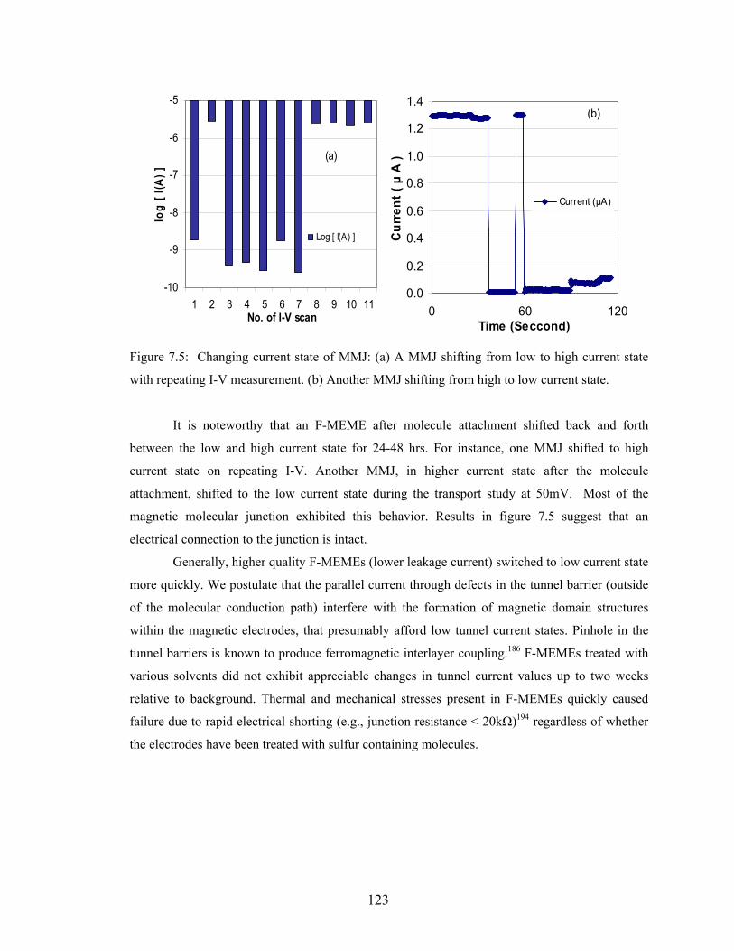
123
-10
-9
-8
-7
-6
-5
1 2 3 4 5 6 7 8 9 10 11No. of I-V scan
log
[ I(A
) ]
Log [ I(A) ]
(a)
0.0
0.2
0.4
0.6
0.8
1.0
1.2
1.4
0 60 120Time (Seccond)
Cur
rent
( µ
A )
Current (µA)
(b)
Figure 7.5: Changing current state of MMJ: (a) A MMJ shifting from low to high current state
with repeating I-V measurement. (b) Another MMJ shifting from high to low current state.
It is noteworthy that an F-MEME after molecule attachment shifted back and forth
between the low and high current state for 24-48 hrs. For instance, one MMJ shifted to high
current state on repeating I-V. Another MMJ, in higher current state after the molecule
attachment, shifted to the low current state during the transport study at 50mV. Most of the
magnetic molecular junction exhibited this behavior. Results in figure 7.5 suggest that an
electrical connection to the junction is intact.
Generally, higher quality F-MEMEs (lower leakage current) switched to low current state
more quickly. We postulate that the parallel current through defects in the tunnel barrier (outside
of the molecular conduction path) interfere with the formation of magnetic domain structures
within the magnetic electrodes, that presumably afford low tunnel current states. Pinhole in the
tunnel barriers is known to produce ferromagnetic interlayer coupling.186 F-MEMEs treated with
various solvents did not exhibit appreciable changes in tunnel current values up to two weeks
relative to background. Thermal and mechanical stresses present in F-MEMEs quickly caused
failure due to rapid electrical shorting (e.g., junction resistance < 20kΩ)194 regardless of whether
the electrodes have been treated with sulfur containing molecules.

124
7.4.1.2 Molecular Reach vs. Tunnel Barrier Thickness
To probe the possibility that uncontrolled surface conduction is responsible for the
unusual experimental conduction behavior, we prepared electrodes with varying insulator layer
(Al2O3) thicknesses,40 while keeping all other factors identical. From X-ray crystallographic data,
we estimate the sulfur-sulfur contact to be ~2.6 nm for MMC and we engineered F-MEMEs with
alumina layer thicknesses ranging from 2.0 to 4.0 nm. The Al2O3 barrier thicknesses were
measured via AFM and Simmons fitting of the tunnel current of bare electrodes prior to treatment
with MMC, figure 7.6(b). We observe that F-MEMEs with 4 nm barrier thickness did not exhibit
change in transport after the treatment with MMC, Figure 6(a),40 unlike the dramatic change seen
with F-MEMEs with 2 nm barrier, figure 7.6(b). However, when the Al2O3 layer thickness is
smaller than the distance between the sulfur-sulfur contacts, the tunnel current is 4-20 times
larger and diminishes rapidly with increasing time, approaching nA values after approximately
seven hours.
0
3
6
9
0 0.02 0.04 0.06 0.08 0.1Voltage ( V )
Cur
rent
( n
A )
Thick barrier F-MEMEWith MMC
( a )
0.0
2.0
4.0
0 0.05 0.1
Voltage ( V )
Cur
rent
( µ
A )
Bare Co/NiFe/Al2O3/NiFeWith MMCAfter 24 Hours
3.2 nA
( b )
Figure 7.6: Electrical behavior of F-MEME treated with MMC. (a) I vs. V plot for F-
MEMEs with 3.5 nm Al2O3 barrier. (b) Response of MMC on F-MEME with 2 nm
barrier thickness.

125
7.4.1.3 Device current state with 1,20-Dithioeicosane treatment:
-2.5
0.0
2.5
-0.4 -0.2 0 0.2 0.4Voltage ( V )
Cur
rent
( μ
A )
Bare F-MEMEWith n-Dithiol Eicosane
Figure 7.7: Voltage dependence of current for bare and 1,20-dithioeicosane
functionalized F-MEME.
To probe if molecules containing unpaired electrons in transition metal centers are
necessary to exhibit low tunnel current states, a series of F-MEMEs was treated with diamagnetic
1,20-dithioeicosane, which is long enough to span a 2 nm Al2O3 insulator gap to produce
molecular conduction channels. The treatment (same process as used for MMC attachment) of F-
MEME with 1,20-dithioeicosane40 (2 mM) followed by washing in dichloromethane(20mL), 2-
propanol (20 mL) and DI water(40mL) and then the drying of samples under an N2 gas stream,
afforded a series of devices containing chemisorbed diamagnetic dithiols. The F-MEME
electrodes exhibited significant increases in tunnel current, not the dramatic current suppression
as observed after attachment of MMC, figure 7.7.
7.4.1.4 Electrode composition and molecular junction transport behavior:
The reproducible and dramatic changes in tunnel current values (nA or pA state) are
found only when magnetic molecular clusters (MMC) and ferromagnetic metals are present. In
particular, the dramatic current reduction is only seen for [Co(10-x nm)/NiFe(x nm)/-
Al2O3(~2.0nm)/NiFe(8-12nm)] F-MEMEs functionalized with MMC. Here x varies between 3-5
nm. In our magnetic measurement we have observed that the coercive field for the bottom
electrode is nearly 5 fold higher than that for the top NiFe electrode. In the ferromagnetic
resonance study also we observed that the top and bottom electrodes behave quite differently. The
resonance mode position for the bottom electrode (Co/NiFe) and top electrode (NiFe) were found
to be at 720 Oe and 1140 Oe, respectively. Bare F-MEME is found to exhibit weak

126
antiferromagnetic coupling via insulator. Extensive details of magnetic studies of F-MEME and
the effect of MMC on its magnetic attributes are presented in chapter 6. We have observed that
changes in the configuration of the top and bottom electrodes produce a dramatic effect on the
molecular cluster response. It was found that the composition of an F-MEME’s magnetic
electrodes was critical in enabling a molecular spin device’s current switchability by the magnetic
field. Details of the effect of electrode composition on the molecular spin device are furnished in
appendix A6. We observed that if the top and bottom electrodes are of the same ferromagnetic
metal, current suppression could not stabilize. For instance, F-MEMEs with both electrodes made
up of NiFe, just produced a stable current increase, figure 7.8. The ferromagnetic resonance study
exhibited that this configuration does not show highly distinctive modes for the top and bottom
electrodes, suggesting a stark difference in the magnetic property of this F-MEME with respect to
the F-MEME with a Co/NiFe bottom electrode. The difference in the coercivity of two magnetic
electrodes was found to be critical for observing Kondo splitting of C60 based molecular
junction13 and tunneling magneto resistance.18
0.0
0.3
0.6
0.9
1.2
1.5
1.8
0 0.02 0.04 0.06 0.08 0.1
Voltage (V)
Cur
rent
( μ
A )
Bare NiFe-Al2O3-NiFeWith MMCAfter 24 HrsAfter 48 Hrs
Figure 7.8: Tunnel current vs. voltage behavior for NiFe(12)/Al2O3(2)/NiFe(12).
We have also prepared a series of nonmagnetic [Ta(12 nm)/Al2O3(2.5 nm)/Ta(12 nm)]
electrode junctions to investigate the apparent requirement that ferromagnetic electrodes are
necessary for the dramatic current reduction.40 The treatment of these electrodes with either 1,20-
dithioeicosane or MMC did not show the dramatic changes in tunnel current (nA or pA state)
relative to background values.7 Combining the results of these two systems suggests that in order
to produce the dramatic change in transport (nA or pA current state), MMCs are required to be
attached across ferromagnetic F-MEMEs (Co/NiFe/Al2O3/NiFe).
127
7.4.1.5. Chemical and Oxidative Stability of F-MEMEs
To further investigate the effects of sulfur-containing molecules on electrical transport
behavior, a series of electrodes was treated with organic thiols of varying chain lengths. In two
experiments, electrodes were treated with CH2Cl2 solutions of either 1-butanethiol (2mM) or 1-
dodecanethiol (5mM), which afforded negligible changes in F-MEME transport (~17 %), relative
to a bare F-MEME’s current value. Furthermore, the observed tunnel currents are far below those
seen for electrodes decorated with MMC (300-5000% increase) or 1,20-dithioeicosane. We
postulate that short alkanethiols (C4–C10) cannot span the insulator gap to assist in conduction.
To further probe the stability of the electrodes and the role of surface oxides in transport
behavior, we purposefully oxidized several electrodes with plasma of various energies. Oxygen
plasma (20W RF; P(O2)=50mtorr) treatment (conditions) or heating of electrodes to 100ºC in air
for 10 minutes did not significantly alter the transport properties relative to freshly prepared
samples. However, increasing the plasma energy (100W RF, P(O2)=50mtorr) quickly induced
catastrophic tunnel barrier failure; that is likely due to significant charging of the samples during
plasma treatment or the generation of thermal stresses. The formation of surface oxides at or near
ambient conditions does not appear to significantly alter the F-MEME transport properties. Even
an improvement in the switching field of the tunneling magneto resistance device was observed
after a plasma treatment of ion milled magnetic tunnel junction.198 Interestingly, we observed that
the burning of molecules by the oxygen plasma from the circumference of F-MEME dots
reversed the molecule effect; the bare sample’s magnetic modes were recovered, chapter 6.
7.4.1.6 Quality of exposed edge of F-MEME for molecule attachment (Ion Milling vs. Lift-
off based F-MEME Fabrication):
The exposed side edge of F-MEME is crucial for allowing molecules to bridge over the
insulator gap. Producing an exposed metal/insulator/metal junction by another fabrication route
and having the same current reduction/magnetic ordering effects can be viewed as a supportive
experiment for the conclusions of this work. Given that Ar ion milling is an established method
for generating exposed edges of multilayer films normal to their growth planes, we prepared
several F-MEMEs using the ion milling approach, figure 7.9(b). Engineering protocols and
conditions are identical to those described for electrodes using lift-off approaches except for ion-
milling of the multilayer edge.40 During the ion beam milling (using FISCHIONE 1010 ion mill),
samples are cooled by liquid N2 to minimize photoresist hardening. TEM studies have confirmed
that a uniform and sharp edge is obtained on ion-milled magnetic tunnel junctions.10 We observed
that F-MEME samples, prepared with ion milling, possessed an exposed edge; a sharp exposed

128
edge allowed the MMC attachment. The MMC attachment resulted in the identical transport
response, figure 7.9(c), as seen with the samples with lift-off produced exposed edges, Figure
9(a). However, thermal stresses introduced in samples during milling and/or cooling resulted in
severe tunnel junction instabilities, poor reproducibility, and short device lifetimes.199 Further
discussion about exposing the edge of F-MEMEs for molecule attachment is given in appendix
A1.
(b)
(a)
Ion milled
Lift-off produced edge
-10
-9
-8
-7
-6
-5
Bare F-MEME w ith MMC After 48 Hrs
Log(
I (A
))
Liftoff producededge
Ionmilled edge
(c)
Figure 7.9: Comparative study of current at 100mV before and after MMC attachment on F-
MEME produced by liftoff and ion milling methods.
7.4.1.7 Bottom electrode stability:
Bottom
Bottom
(a)
(b)
Top
Top
-10
-9
-8
-7
-6
-5
Bare with MMC After 48 Hrs
Log(
curr
ent (
A))
X- Pattern
T-Pattern
(c)
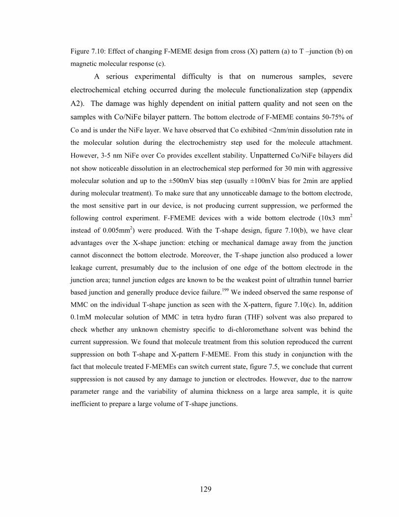
129
Figure 7.10: Effect of changing F-MEME design from cross (X) pattern (a) to T –junction (b) on
magnetic molecular response (c).
A serious experimental difficulty is that on numerous samples, severe
electrochemical etching occurred during the molecule functionalization step (appendix
A2). The damage was highly dependent on initial pattern quality and not seen on the
samples with Co/NiFe bilayer pattern. The bottom electrode of F-MEME contains 50-75% of
Co and is under the NiFe layer. We have observed that Co exhibited <2nm/min dissolution rate in
the molecular solution during the electrochemistry step used for the molecule attachment.
However, 3-5 nm NiFe over Co provides excellent stability. Unpatterned Co/NiFe bilayers did
not show noticeable dissolution in an electrochemical step performed for 30 min with aggressive
molecular solution and up to the ±500mV bias step (usually ±100mV bias for 2min are applied
during molecular treatment). To make sure that any unnoticeable damage to the bottom electrode,
the most sensitive part in our device, is not producing current suppression, we performed the
following control experiment. F-FMEME devices with a wide bottom electrode (10x3 mm2
instead of 0.005mm2) were produced. With the T-shape design, figure 7.10(b), we have clear
advantages over the X-shape junction: etching or mechanical damage away from the junction
cannot disconnect the bottom electrode. Moreover, the T-shape junction also produced a lower
leakage current, presumably due to the inclusion of one edge of the bottom electrode in the
junction area; tunnel junction edges are known to be the weakest point of ultrathin tunnel barrier
based junction and generally produce device failure.199 We indeed observed the same response of
MMC on the individual T-shape junction as seen with the X-pattern, figure 7.10(c). In, addition
0.1mM molecular solution of MMC in tetra hydro furan (THF) solvent was also prepared to
check whether any unknown chemistry specific to di-chloromethane solvent was behind the
current suppression. We found that molecule treatment from this solution reproduced the current
suppression on both T-shape and X-pattern F-MEME. From this study in conjunction with the
fact that molecule treated F-MEMEs can switch current state, figure 7.5, we conclude that current
suppression is not caused by any damage to junction or electrodes. However, due to the narrow
parameter range and the variability of alumina thickness on a large area sample, it is quite
inefficient to prepare a large volume of T-shape junctions.

130
7.4.2 Effect of temperature light and magnetic field:
7.4.2.1 Effect of temperature:
Variation in temperature dramatically affected the transport of magnetic molecular
junctions (MMJs), figure 7.11. At high temperatures (400 K), magnetic ordering and transport of
MMJs changed significantly. In a study three MMJs, initially in nA current state at RT, were
heated to 400K and then cooled to RT; current measured at RT on all three junctions showed that
the current value increased to 2-5μA levels at 100mV. Such an increase is also possible when a
tunnel junction undergoes breakdown of a tunnel barrier. Upon cooling to 77 K, three junctions
exhibited lowest pA current state, which may be due to two reasons: (a) MMJs transport is
dominated by the defects in tunnel barrier showing the Pool-Frenkel37 type mechanism, (b)
magnetic electrodes resumed the magnetic ordering required to exhibit low current state, lost by
MMJs during heating to 400K temperature. Interestingly, after warming the MMJs from 77K to
298 K, three MMJs under study persisted in the low-current state (nA-pA), and no device reached
the original µA current state. Three control samples remained in nA current state or lower for
more than 30 days until the second heating of MMJ to 400 K was performed. This observation
unambiguously suggests that the role of defects in changing current state with temperature
variation is highly unlikely. Switching an MMJ among three current states is consistent with the
loosing and reinstating of molecule enabled magnetic ordering.
The effect of thermal cycles on bare junction transport was studied to ensure that the
bridging of MMC on F-MEME is required to enter low current state (nA or pA states). The
cooling of a bare F-MEME to 77K did not induce low current state, figure 7.11(b). The annealing
of a bare F-MEME at 450 K for 30 min modestly decreased current of bare electrodes. Slow
heating rate (5 K/Min), similar to what we used for the heating of three MMJs, was utilized.
Presumably, improvement in tunnel barrier during annealing17 is the reason behind reduction in
the current of a bare F-MEME, figure 7.11(c). Heating performed at a faster rate, 1-10 K/sec, in
ambience condition, produced either no change in transport or a permanent current increase due
to tunnel barrier breakdown. This is opposed to the case of electrodes treated with MMC in which
thermal annealing disrupts the low current state (nA or pA) to get into the high current state (μA).
The heat treatment of F-MEME with MMC switching from nA state to μA (high temperature)
and then to pA state (77K) reoccurred on an MMJ, Table 7.1. In the case of a tunnel barrier with
atomic defects, such as TaOx, transport was found to be temperature dependent and was
following the Pool-Frenkel type mechanism.178 We have found that after returning to the RT from
the heating and cooling step, generally the device resumed its starting current level, unlike MMJs
where different current levels were observed with respect to temperature.

131
-13-12-11
-10-9-8-7
-6-5
RT 400 K toRT
77 K * 77 K toRT
Log
Cur
rent
( A
)MMJ 1MMJ 2MMJ 3
(a)
-0.25
0.00
0.25
-0.5 0 0.5Voltage (V)
Cur
rent
( µ
A )
Before coolingAfter cooling at 77K for
(b)
-12
-6
0
6
12
-0.5 0 0.5Voltage (V)
Cur
rent
( µ
A )
BeforeAfter annealing
(C)
Figure 7.11: (a) Effect on device transport after heat treatments of three different MMJ samples.
Measurements made at room temperature (RT) except for * marked study that was made at 77K.
(b) Electrodes cooled to 77K (45 min.) and then heated to 300 K (1-5 ºC min-1), and (c) Impact of
annealing time and temperature on I vs V behavior of F-MEME.
Table 7.1: Effect of heating -cooling cycle was studied twice on the same MMJ.
1st cycle 2nd cycle
At RT 3.8±1x10⁻⁹ 2.0±1.0 1x10⁻⁹
After annealing at 150 C for 10 min & cooling to RT 3.2 ±1x10⁻⁶ 5.0±2.01x10⁻⁶
After cooling to 77K ~5 ±2 1x10-13 ~4±2x10-13
After warming up from 77K to RT ~1-10 1x10-12 ~1-10 1x10-12
7.4.2.2 Effect of light:
As illustrated in figure 7.12(a), the photo excitation of MMJs in the intermediate (nA)
state showed preferential current at 0V bias. The photocurrent direction is consistent with electron
flow from the bottom (Co/NiFe) electrode. Since there is no Schottky barrier or other means of
producing inbuilt electric field within the barrier due to the symmetrical tunnel barrier and
molecule,1 there should not be a driving force to preferentially allow for a net flow of
electrons/holes from the bottom to the top electrode, unless selective photoexcition of spin-
oriented electrons in the ferromagnetic films of the MMJs, have more favorable states to tunnel
into the top electrode. The flux of photons (~100 mW white light) over the entire 5x5 µm2 area of
the MMJs would correspond to the 0.8 nA of observed current with ideal conversion (100%).
Since the area of molecules at the edge of the pattern is ~103 less, it is unlikely that the observed
photocurrent is due to the photoexcitation of electrons present within the tethered cluster, since
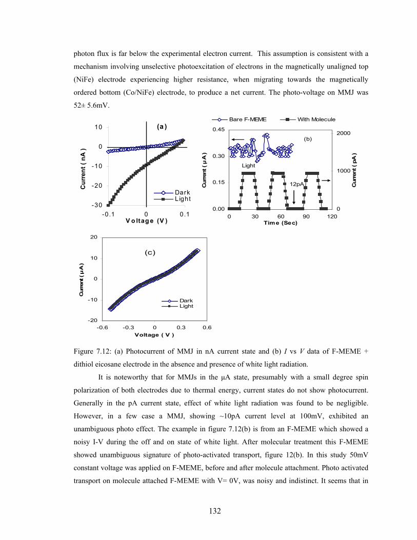
132
photon flux is far below the experimental electron current. This assumption is consistent with a
mechanism involving unselective photoexcitation of electrons in the magnetically unaligned top
(NiFe) electrode experiencing higher resistance, when migrating towards the magnetically
ordered bottom (Co/NiFe) electrode, to produce a net current. The photo-voltage on MMJ was
52± 5.6mV.
-30
-20
-10
0
10
-0.1 0 0.1V o ltag e (V )
Cur
rent
( nA
)
DarkLight
(a )
0.00
0.15
0.30
0.45
0 30 60 90 120Time (Sec)
Cur
rent
( µ
A )
0
1000
2000
Cur
rent
( pA
)
Bare F-MEME With Molecule
12pA
(b)
Light
-20
-10
0
10
20
-0.6 -0.3 0 0.3 0.6Voltage ( V )
Cur
rent
( µ
A )
Dark Light
(c)
Figure 7.12: (a) Photocurrent of MMJ in nA current state and (b) I vs V data of F-MEME +
dithiol eicosane electrode in the absence and presence of white light radiation.
It is noteworthy that for MMJs in the μA state, presumably with a small degree spin
polarization of both electrodes due to thermal energy, current states do not show photocurrent.
Generally in the pA current state, effect of white light radiation was found to be negligible.
However, in a few case a MMJ, showing ~10pA current level at 100mV, exhibited an
unambiguous photo effect. The example in figure 7.12(b) is from an F-MEME which showed a
noisy I-V during the off and on state of white light. After molecular treatment this F-MEME
showed unambiguous signature of photo-activated transport, figure 12(b). In this study 50mV
constant voltage was applied on F-MEME, before and after molecule attachment. Photo activated
transport on molecule attached F-MEME with V= 0V, was noisy and indistinct. It seems that in

133
the nA current state, an MMJ possesses optimum difference in the spin polarization or magnetic
ordering of two electrodes at RT to produce photocurrent under light radiation. A discussion on
the effect of magnetic molecular cluster on the spin polarization of magnetic electrodes is
presented elsewhere in this chapter.
Insignificant photocurrent effects are observed in the absence of the chemisorbed MMC
clusters or with organic (diamagnetic) molecules tethered across MMJ. It was observed that photo
current was only obtained when magnetic molecules were self assembled across the F-MEME
device. No photo current was observed on F-MEME + dithiol eicosane, figure 7.12(c), and
NiFe/AlOx(2nm)/NiFe+MMC systems. Failed tunnel junction (with low ohmic resistance) also
did not produce the photo current presumably due to a parallel conduction path through defects of
non spin oriented electrons. However, we have seen photovoltaic effect in
Ta(12nm)/TaOx(2nm)/Ta(12nm) tunnel junctions; graded density of atomic defects within a
TaOx barrier not only enhanced the light absorption capability of ~2.5nm TaOx, but also
produced an inbuilt electric field. We found that such photovoltaic effect is very transient with
respect to the change in temperature, and exposure duration to white light. Whereas, photovoltaic
effect on MMJ was found to be stable for several months; it did not vanish or change even after
30min of high intensity light radiation. Sensitivity of photovoltaic effect of MMJ towards a
magnetic field also supports its origination from the molecule induced magnetic ordering of
electrodes. The application of inplane magnetic field, which generally switched the MMJ’s
current to lower level, diminished the photo current to become negligible. However, photo effect
re-appeared as MMJ resumed the nA current state. Photocurrent on Ta/TaOx/Ta was indifferent
to magnetic field effect; with degrading TaOx barrier photocurrent became negligible
irreversibly.
7.4.2.3 Effect of magnetic field:
Transport of the ferromagnetic multilayer edge molecular electrode (F-MEME) before
and after the MMC attachment was studied, in the magnetic field varying between ±300 Gauss
and after the magnetization by the static 0.45T magnetic field. For the application of weak in-
plane magnetic field, bare F-MEME generally did not show a sharp magneto current change up to
250 Gauss. Presumably, it is due to the inability to pin the magnetization of one layer and rotate
the magnetization of another layer independently. We obtained clear loop during the magneto-
transport study, figure 7.12(a). Interestingly, it was found that after the attachment of magnetic
molecular cluster a F-MEME exhibited almost similar magneto-transport loop in high and low
current state, figure 7.12(b-c). However, data was significantly noisy in the transient high current
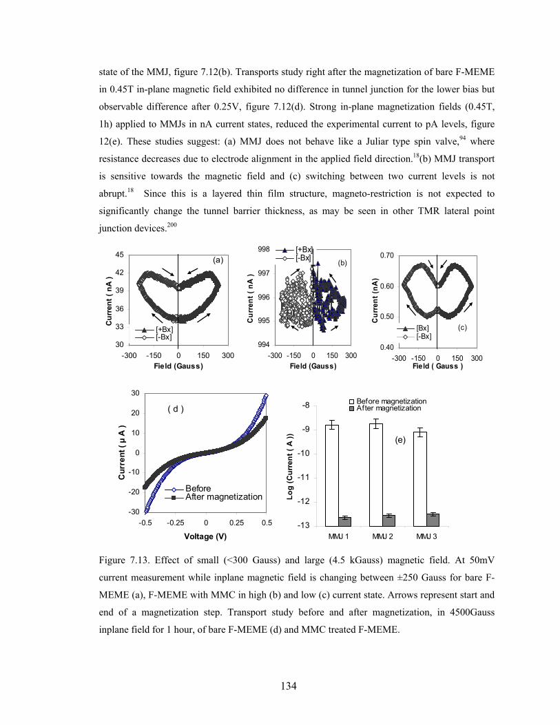
134
state of the MMJ, figure 7.12(b). Transports study right after the magnetization of bare F-MEME
in 0.45T in-plane magnetic field exhibited no difference in tunnel junction for the lower bias but
observable difference after 0.25V, figure 7.12(d). Strong in-plane magnetization fields (0.45T,
1h) applied to MMJs in nA current states, reduced the experimental current to pA levels, figure
12(e). These studies suggest: (a) MMJ does not behave like a Juliar type spin valve,94 where
resistance decreases due to electrode alignment in the applied field direction.18(b) MMJ transport
is sensitive towards the magnetic field and (c) switching between two current levels is not
abrupt.18 Since this is a layered thin film structure, magneto-restriction is not expected to
significantly change the tunnel barrier thickness, as may be seen in other TMR lateral point
junction devices.200
30
33
36
39
42
45
-300 -150 0 150 300Field (Gauss)
Cur
rent
( nA
)
[+Bx][-Bx]
(a)
994
995
996
997
998
-300 -150 0 150 300Field (Gauss)
Cur
rent
( nA
)[+Bx][-Bx] (b)
0.40
0.50
0.60
0.70
-300 -150 0 150 300Field ( Gauss )
Cur
rent
(nA
)
[Bx][-Bx]
(c)
-30
-20
-10
0
10
20
30
-0.5 -0.25 0 0.25 0.5
Voltage (V)
Cur
rent
( µ
A )
BeforeAfter magnetization
( d )
-13
-12
-11
-10
-9
-8
MMJ 1 MMJ 2 MMJ 3
Log
(Cur
rent
( A
))
Before magnetizationAfter magnetization
(e)
Figure 7.13. Effect of small (<300 Gauss) and large (4.5 kGauss) magnetic field. At 50mV
current measurement while inplane magnetic field is changing between ±250 Gauss for bare F-
MEME (a), F-MEME with MMC in high (b) and low (c) current state. Arrows represent start and
end of a magnetization step. Transport study before and after magnetization, in 4500Gauss
inplane field for 1 hour, of bare F-MEME (d) and MMC treated F-MEME.
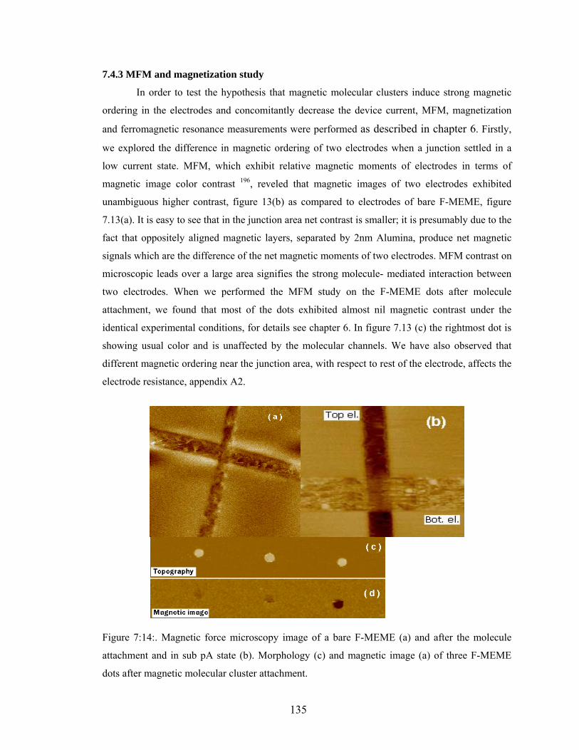
135
7.4.3 MFM and magnetization study
In order to test the hypothesis that magnetic molecular clusters induce strong magnetic
ordering in the electrodes and concomitantly decrease the device current, MFM, magnetization
and ferromagnetic resonance measurements were performed as described in chapter 6. Firstly,
we explored the difference in magnetic ordering of two electrodes when a junction settled in a
low current state. MFM, which exhibit relative magnetic moments of electrodes in terms of
magnetic image color contrast 196, reveled that magnetic images of two electrodes exhibited
unambiguous higher contrast, figure 13(b) as compared to electrodes of bare F-MEME, figure
7.13(a). It is easy to see that in the junction area net contrast is smaller; it is presumably due to the
fact that oppositely aligned magnetic layers, separated by 2nm Alumina, produce net magnetic
signals which are the difference of the net magnetic moments of two electrodes. MFM contrast on
microscopic leads over a large area signifies the strong molecule- mediated interaction between
two electrodes. When we performed the MFM study on the F-MEME dots after molecule
attachment, we found that most of the dots exhibited almost nil magnetic contrast under the
identical experimental conditions, for details see chapter 6. In figure 7.13 (c) the rightmost dot is
showing usual color and is unaffected by the molecular channels. We have also observed that
different magnetic ordering near the junction area, with respect to rest of the electrode, affects the
electrode resistance, appendix A2.
Figure 7:14:. Magnetic force microscopy image of a bare F-MEME (a) and after the molecule
attachment and in sub pA state (b). Morphology (c) and magnetic image (a) of three F-MEME
dots after magnetic molecular cluster attachment.

136
-150
-100
-50
0
50
100
150
-5000 0 5000Field (Oe)
Mom
ent (
µ e
mu)
Bare FMEMEw ith MMC
150 K
(a)
-100000
-50000
0
50000
100000
0 500 1000 1500Field ( Oe )
FMR
Sig
nal (
a.u.
)
Bare magnetic dotsWith Molecule
(b)
Figure 7.15. (a) Magnetization study of F-MEME dot pattern before and after MMC attachment
at 150K. (b) Ferromagnetic resonance study of F-MEME before and after magnetic molecule
attachment at RT.
To further probe the reason behind the difference in magnetic contrast of two electrodes
after MMC attachment on F-MEME, magnetization and ferromagnetic resonance measurements
were performed. Samples with F-MEME dots (~7000-14,000 dots each of ~3 μm diameter and
[Ta/Co/NiFe/AlOx/NiFe] configuration) were prepared in order to maximize the signal intensity
from ferromagnetic metals. Details of magnetization and ferromagnetic resonance study on F-
MEME dot patterns are furnished in chapter 6. Both studies clearly suggest the emergence of
extremely strong antiferromagnetic coupling between ferromagnetic electrodes of F-MEME due
to molecule attachment. Before addition of molecules, the dots were weakly antiferromagnetic,
exhibiting a saturation magnetization value of ~1.0 × 10⁻⁴ emu. After cluster addition, a dramatic
drop in the magnetic moment was observed (~90%) consistent with antiferromagnetic alignment
of the top and bottom NiFe layers.188
In ferromagnetic resonance study two modes, acoustic and optical, of F-MEME dots
almost disappeared from the spectra when magnetic molecular clusters were bridged on the
exposed edges of the F-MEME dots. A related theoretical study has shown that when interlayer
ferromagnetic coupling between two layers crosses a critical limit then, two layers get aligned
antiparallel to each other. In this situation, the weaker mode flattens out and the stronger mode
shifts to higher resonance field.191 We conjecture that new resonance position for the molecule
treated F-MEME dots is beyond the range of magnetic field we could study on our samples. From
137
our magnetic study we conclude that magnetic molecular cluster induced antferromagnetic
coupling, which in turn contributed towards producing ~6 orders of current suppression.
7.5 Discussion:
We have observed 3-6 orders current suppression on ferromagnetic-multilayer edge
molecular electrode (F-MEME), typically a magnetic tunnel junction, after the attachment of
magnetic molecular clusters (MMC). Spin dependent transport of a magnetic tunnel junction
strongly depends on the relative direction of magnetizations and degree of spin polarization of
two electrodes.18 Since current suppression is observed for the complete device comprising
molecular transport channels and ~25μm2 tunnel junction area, we surmise that it is only possible
when two ferromagnetic electrodes are anti-parallel to each other and highly spin polarized. Other
possibilities of defining current suppression, in terms of quantum interference among tunneling
paths within a molecular magnet30 and antiferromagnetic ordering on a molecular channel
allowing >6 order resistance change due to magnetic field,30 cannot describe the shutting down of
transport via planar junction.32
In a magnetic tunnel junction, comprising ferromagnetic layers with~40% spin
polarization,196 sufficient population of minority spins is present close to the Fermi level.17
Minority spin can produce significantly high transport even when majority spins of two
ferromagnetic electrodes are in an anti-parallel state.26 In magnetic characterization of F-MEME,
details in chapter 6, we have observed that MMC produced strong antiferromagnetic inter-layer
exchange coupling. Strong interlayer coupling was also found to decrease the magnetic contrast
of F-MEME dots. Disappearance of magnetic contrast196 is consistent with the cancellation of
magnetization of one layer by the magnetization of another layer, at 2nm distance. In order to
calculate the value of spin polarization, required to observe ~3 order current decrease in the
present case, we assume that the highest current level after molecule attachment on F-MEME
current level is similar to the case when two electrodes are parallel to each other; after MMC
attachment F-MEME current is 3 order smaller at RT and two ferromagnetic electrodes are anti-
aligned. Current of a magnetic tunnel junction in parallel (IP) and antiparallel state (IAP) of
electrode can be given by )( 22↓↑ +∝ DDI P and ↓↑∝ DDI AP ..2 , respectively.81 Where D↑ and D↓
are the density of spin up and spin down electron in the magnetic electrode; expression for spin
polarization (P) is )/()( ↓↑↓↑ +− DDDD . For IP= 1μA and IAP=1nA, value of P comes out to be
>99.999 %. This level of spin polarization is completely unprecedented and would be an
important breakthrough for spin-electronics.

138
What makes a regular ferromagnet highly spin polarized? What is the energy cost
involved and from where is it sourced? These are the important questions to answer. Total energy
of a ferromagnet is the sum of Heisenberg energy, dipolar energy, magnetic anisotropy energy
and Zeeman energy.191 The last term, Zeeman energy, also depends upon the external energy.46
Degree of spin polarization in bulk ferromagnetic metals is essentially defined by the energy gap
between spin-up and spin-down bands, known as Stoner splitting and it is akin to Zeeman
splitting.191,196 For instance, in Fe stoner splitting and spin polarization are ~1.4eV and ~40%,
respectively.196 Enhancement of spin polarization will require a larger splitting; for larger splitting
one has to supply required energy by external means, generally in the form of a magnetic field.46
However, it is worth noticing that we did not apply magnetic field on molecule treated F-MEME
to produce any energy splitting. It is believed that interlayer coupling effectively acts as an
external field.201 Our molecule provided localized density of states amid tunnel barrier; molecular
transport analysis suggested that for molecular channels barrier thickness was found to be
~1.2nm, as opposed to 2nm barrier thickness of bare F-MEME.40 In this case, molecular array
appear to work as an additional electrode inserted at the center of alumina barrier, barrier
thickness after molecule attachment is ~1nm. According to Slonczewski’s model94 interlayer
exchange coupling (J) via insulator is given by186:
dkB ekkkkd
kkkkkkkkJ .2
22222222
223
)()()())(( −
↓↑
↑↓↓↓↓↑
+++−−
=π
ϕ (7.1)
Here, k↑ and k↓ are the wave vector for the spin up and spin down electron in ferromagnet, wave
vector for the electron in tunneling barrier is given by h/..2 mk Bϕ= , where, Bϕ is barrier
height, m is mass of electron and h is plank’s constant. For the NiFe(80% Fe) metal, which is in
direct contact of molecular channels, we conjectured that using bulk parameters for the Fe is
reasonable. For Fe, k↑≈1.09Å-1 and k↓≈0.43 Å-1.186 The distance between the two nearest
electrodes is d. According to our previous study the barrier thickness (Barrier height) for the
alumina and molecular barrier are 2nm (1eV) and 1.2nm (0.8eV), respectively. This relation
clearly produces ~4 orders enhancement, from -7.36x10¹² erg/cm2 to -7.33x10¹⁶ erg/cm2, in
coupling energy when barrier thickness (barrier height) was reduced from 2nm (~1eV) to 1.2nm
(~0.74eV). It should be noted that calculated values very different from the experimental values
and only appear useful for the qualitative understanding. We find it difficult to conclude that
calculated increase by ~4orders is the reason behind dramatic change in transport and magnetic

139
properties of F-MEME; in the experimental studies, reducing down the MgO barrier thickness to
0.5nm though produced a significantly strong, yet measurable, antiferromagnetic coupling, but
no remarkable change in magnetic properties of the magnetic electrodes was reported.186
The important point to note is that change in interlayer exchange coupling strongly
depends on the nature of the spacer. Semiconductor spacers have shown interlayer exchange
coupling strength to a much higher extent than that seen with insulator of similar thickness.186
Slonczewski’s model did not incorporate the important details, such as the degree of spin-orbit
coupling and hyperfine splitting of the barrier, in calculating interlayer exchange coupling.17 Spin
orbit-coupling and hyperfine splitting are significantly different for organic molecules in
comparison with insulators.26,27 Another important aspect which can make a strong difference is
barrier height of the spacer between the two nearest densities of state partaking in transport.
Barrier height between molecular level and metal Fermi level is observed to be affected by the
image charges on the metallic electrodes, induced by the charged molecule.35
(c)
NiNi
Ni
Fe
Fe
Fe
Fe
CN
CN
CN
CNFM1 FM2
FM1 FM2
FM1 FM2
(a)
(b)
Figure 7.16: (a) An impurity between two metal electrodes, (b) molecule between two metal
electrodes but only at the edges. (c) One slice of (b) showing molecule between two electrodes,
molecules structure is simplified for clarity, all the ligands, H bonds CN bond (other than the
front face of cluster cube) omitted.
A recent study discussing the role of atomic impurities around the center of the tunnel
barrier, figure 7.16(a), producing energy level close to the Fermi level, exhibited an enhancement

140
in exchange coupling energy by ~3 orders.95 It was shown that the effect of impurities on the
magnetic tunnel junction transport is additive in nature.95,202 Importantly, it was found that spin
transport is indifferent towards the lateral coordinates of impurities, in the plane parallel to the
electrodes.202
We surmise that 10,000 magnetic molecular clusters attached on the exposed edge of the
F-MEME are akin to well defined impurities, whose position can be precisely controlled, figure
7.16(b-c). Since the molecule in our case also expected to possess a net spin state,3 a strong
antiferromagnetic coupling is expected to arise from the spin dependent hybridization of
molecular level with the spin density of states of ferromagnetic electrodes.56 Experimental
observation of large Kondo splitting, in C60 molecule between two ferromagnetic electrodes, was
explained in terms of a magnetic field arising from the spin-fluctuation induced exchange
coupling between two ferromagnetic electrodes via molecular level.13 Spin fluctuations have also
been observed to play an important role in modifying the magnetization of 2D ferromagnetic
layers coupled by a nonmagnetic layer; however;197 in our case each ferromagnetic electrode is
~10nm thick and hence does not fit well to 2D description. Strong interlayer exchange is likely to
modify the band arrangement of ferromagnetic electrodes;99 theoretical calculation to quantify the
effect of magnetic molecular cluster on the spin polarization of ferromagnetic electrodes is
beyond the scope of this work.99,201 However, according to our estimation, lower bound of
molecule-induced strong antiferromagnetic coupling between two electrode is ~20 erg/cm2;
which is ~ 2 orders higher than the maximum exchange coupling observed via an 0.5nm thick
insulator.186 In summary, there are a number of promising theoretical works97,99 which deals with
the correlation between spin of metal electrodes and spin of molecules which can provide a basis
for the explanation for the observed high spin polarization in this study.
We have also attempted to calculate spin polarization using Sloncczewski’s model as
given below.17
))(())((
2
2
↓↑↓↑
↓↑↓↑
++−−
=kkkkkkkkkkP (7.2)
This model connects the spin polarization to the barrier height of tunneling barrier. Our previous
study suggests that molecular transport is dominated by the alkane tunneling barrier possessing
~0.8eV barrier height; tunneling to and from the core of molecule via alkane tether was found to
be the slowest step.40 The value of polarization, assuming the same effective mass of electrons
for the alumina and tunneling barrier and using the rest of the parameters as mentioned in the
calculation of exchange energy, we found that value of spin polarization for the alumina barrier

141
(~1eV) and alkane barrier (~0.74eV) was -12% and -20%, respectively. We see that this model
predicted significantly different spin polarization before and after molecule treatment. However,
we are unable to explain the origin of extremely large degree of spin polarization due to
molecular clusters, 99.99%, using this conventional approach. Thus it becomes very
important to look at the available electronic states of the conducting metal cluster.
The cluster core is composed of alternating Ni(II) and Fe(III) metals at the corners
of a cube bridged by a cyano group that induces ferromagnetic ordering at ~10K.
Importantly both the Ni and Fe have available electronic states, of only one spin
orientation, to tunnel into, figure 7.17(c). Ni(III) and Fe(IV) are not stable oxidation
states, so only electron addition to the cluster (i.e. electron transfer not hole transfer) is
plausible. In particular the Fe(III) can be reduced to Fe(II) to have a stable conduction
state (with well defined spin state) before the electron can tunnel out of the system to the
second electrode. From electrochemical data on the molecular clusters in solution, it was
found that the oxidation potential of the Fe(II)/Fe(III) couple is 0.32 V vs. Ag/AgCl
electrode. The cluster also shows a 200mV charging energy to access the next oxidation
state. The resulting relative band structure from known work functions is shown in figure
7.18. Two features are of particular importance. 1st the charging energy of the 4+
molecule brings the molecular HOMO down 0.8V, and is very close to the metal leads
Fermi level. Secondly since the oxidized states are not stable, the electrons cannot leave
the cluster, hence while in equilibrium the Fermi level of the HOMO must be at or below
the Fermi level of the metals resulting in band bending of the alkane barriers. A particular
interesting phenomena is that when the molecule has an added electron charge, the
energy will be raised ~200mV. This is not too far from the observed thermal activation
energy of 300mV seen in chapter 3. This geometry, well defined spin states, and dynamic
energy level changes allow for the cluster to act as a spin filter or pump, possibly
accounting for the high degree of spin polarization.

142
(a)
1nm
~0.8eV
EF
EF
(b)
(d)
NiNi
Ni
Fe
Fe
Fe
Fe
CN
CN
CN
CNFM1 FM2
(c)
Figure 7.17: via molecular state. Right after MMC attachment molecular device in µA current
level (a), exchange of spin polarized electron between two electrodes via molecule (b) electronic
level description of molecule producing spin polarized electrodes (c) resultant spin polarized
ferromagnetic electrodes in nA/pA current sate of molecular junctions.
Ni
Fe Ag
5.1, 4.5, 4.2 eV 3.9 eV
Fe(II/III)-CN
NiFe -Cluster 4+ -NiFe
~ 0.9eV
NiFe -Cluster 3+ -NiFe
~ 0.2eV
Figure 7.18: (a) Approximate band diagram deduced from electrochemical redox potentials. (b)
A charging energy of 0.2eV/charge is seen for the cluster, thus for 4+ cluster, the energy level is
reduced ~0.8eV. Since oxidation of Ni(II) and Fe(III) is not possible, band bending would bring
molecular to Fermi-levels of contacts. Only a single Fe(II/III) d-orbital state is shown for clarity.
Charging of cluster during conduction would raise energy level ~0.2eV above ground state.

143
Dramatic change in magnetic and transport properties of F-MEME is only seen when
magnetic molecular cluster with well defined spin state was bridged along exposed edges, figure
7.17 (b). Two Ni atoms of the core cube of MMC are expected to connect to the Ni atoms of
ferromagnetic layers via alkane barrier, in an ambient condition NiFe was shown to possess
oxidized Fe and elemental Ni.114 An alkane tether, being an organic molecule, is known to
possess long spin coherence length and time, hence making spin exchange between ferromagnetic
electrodes via molecular levels much more effective than that via alumina.26 Bare F-MEME
possessed weak antiferromagnetic coupling; we surmise that two Ni atoms of cluster core,
directly connected to the ferromagnetic electrodes, have empty space for the spin down electron
only, as shown in figure 7.17(c) . Electrode, where spin down (spin up) electron are in the
majority, will transfer the electron spin to the Ni of molecular core with a higher (lower) rate.17,18
Since two Ni atoms are coupled to each other through superexchange9 CN- and Fe atom of the
core, a net spin polarized flux is expected to flow from one electrode to another unless an
equilibrium, producing highly spin polarized ferromagnetic layers, is reached, figure 7.17 (d). We
surmise that summing the spin-dependent wave-function overlap92 of two electrodes via 10,000
molecular clusters produces a magnitude of overlap sufficient to produce situation for super
exchange.9 Under this condition, new equilibrium will require two electrodes to be anti-parallel
with each other and with a high degree of spin polarized.46
7.6 Conclusion
We have successfully prepared molecular spin devices by attaching the magnetic
molecular cluster on the exposed edge of a multilayer edge molecular electrode. 10,000 molecular
bridges between two ferromagnetic electrodes of a 25μm2 planar junction area, suppressed the
current by 3-6 orders below the leakage of bare tunnel junction. High degree of spin polarization
and unprecedented molecule induced antiferromagnetic coupling is found to be the basis of
dramatic change in transport. External energy forms, light, heat and magnetic field, produced
unambiguous effect on transport. Spin dependent hybridization of the magnetic electrodes with
the well defined spin state of the molecular cluster, appears to be the driving force behind the
drastic change in spin polarization. To make molecular device switchable between two or more
current states different configurations of the multilayer’s and the use of molecular clusters are
recommended. Our design, involving photolithography and widely-available thin-film deposition
method, offer a new opportunity to produce robust and highly versatile molecular spin devices
efficiently and economically.

144
Chapter 8
Conclusion
This dissertation showed the successful realization of novel molecular spin devices using a
multilayer edge molecular electrode (MEME) design. MEMEs were prepared by customizing a
classic tunnel junction structure by spanning insulator film with molecular complexes at the
exposed face of patterns. The key steps of MEME fabrication are: (a) fixing the molecular
dimension gap between two thin film metal electrodes, (b) producing exposed edge(s) where
distance between two meal electrodes is equal to the thickness of ultrathin insulator and (c)
bridging of desired molecular channels between two metal electrodes of MEME to transform it
into a molecular device, figure 8.1.
Figure 8.1: A MEME before (a) and after (b) the bridging of magnetic molecular clusters.
8.1 Advantages of MEME devices
(i) Determining the true charge and spin transport characteristic of a molecule:
Since we prepare a robust tunnel junction prior to the bridging of molecular
channels on the exposed edge, one can compare the transport characteristics of
the molecule with respect to the transport attributes of the host MEME tunnel
junction. This attribute is one of the foremost drawbacks of present molecular
devices.
(ii) Easy approach to produce molecular dimension gap: In this work we used thin
film deposition and oxidation to produce insulator of molecular dimension gap.
Thin film deposition and oxidation are highly matured and controllable to

145
produce Angstrom-scale precision. A summary of other strategies to produce
nano-gap is provided in chapter 4.
(iii) Economical and integrable device-fabrication scheme: For the MEME fabrication
we only utilized photolithography and thin film deposition as primary tools.
These tools are widely available around the world and regularly used in
semiconductor technology. Any practical device resulting, such as molecular spin
valve, from our approach is expected to reach the commercial stage rapidly.
Institutions not equipped with hi-tech equipments can perform research using
MEME design to contribute in the advancing field of molecular electronics.
(iv) Freedom to choose a variety of metal electrodes: MEME tunnel junction can
include any metal on which a good quality ultrathin insulator can be grown. This
study used NiFe, Ta, Cu, Pd, Au, and Si. It should be noted that most of the
reported molecular devices utilize Au as a primary electrode metal, due to its
ability to mechanically deform into break junctions and its inherently clean
surface.
(v) Molecular electronics to molecular spintronics: In this dissertation we
have prepared a large number of molecular spin devices simply by using
ferromagnetic metals as top and bottom metal electrode coupled with a
transition metal cyano-cluster. This enabled us to make novel molecular
spin devices for the first time and subsequent observations of a number of
surprising phenomenons arising from metal-molecule interaction.
(vi) Molecule being on the exposed part of MEME can interact with light and
chemical: Molecules on a MEME are in the exposed region where light
radiation and foreign chemical can reach. In the chapter 3, a new form of
chemical sensing was demonstrated with the chemical displacement of top
electrode contact. This attribute adds enormous applications for photo-
active molecular devices, e.g., molecular photovoltaic cells, and chemical
and biosensors.

146
8.2 Achievements of the present doctoral study:
i. Multilayer edge molecular electrodes were prepared. Two key challenges
were: (a) to grow high quality alumina, (b) and to expose the edge(s) of
MEME for the bridging of molecular channels. In order to grow the high
quality alumina effect of mechanical stresses on the electrical properties
and the device life was extensively studied, chapter 2. Using the optimized
condition for the growth of alumina, MEME were prepared, chapter 3. For
exposing the edge of a tunnel junction, two approaches were adopted. In
one approach a tri-layer with metal-insulator-metal pattern was ion milled
to produce an atomically sharp vertical cut. At the ion milled produced
edge a minimum gap between two electrodes was equal to the insulator
film thickness. However, due to the stresses introduced during ion milling,
this approach was only used for performing the control experiments. In
another approach, photolithography-liftoff was utilized, chapter 3. In this
methodology a bottom metal electrode alumina and top metal electrode
were deposited through the same photo resist window. The idea was to
keep the lateral dimension of the alumina and the top electrode the same;
in this case the minimum gap between the two metal electrodes is equal to
the thickness of ultrathin alumina insulator, figure 8.1(b).
ii. Simplification of MEME fabrication scheme: The success of a MEME
fabrication scheme is critically dependant on the thickness, quality and the
edge profile of the alumina insulator. We produced a simpler version of
MEME electrodes just by oxidizing bottom electrode TaOx through well
controlled plasma oxidation method, chapter 4. Under this approach, the
need for depositing Al was replaced with the utilization of an nm thick
segment of bottom electrode of an oxidizable metal, Ta in the present case.
Rest of the fabrication was the same as for photolithography-liftoff
produced MEME. Though the overall device current was lower due to Ta
contacts, the molecular transport mechanism from this scheme
corroborated with the MEME based on alumina insulator.

147
iii. Photovoltaic effect of Ta/TaOx/Ta: During our attempts to produce TaOx
based molecular electrodes, it was found that Ta/TaOx/Ta junction
showed significant photovoltaic effect with ~9% energy efficiency,
Chapter-5. A ~3nm TaOx with high graded density of atomic defects was
found to show remarkably high light absorbance. The graded density
profile of atomic defects in TaOx produced an inbuilt electric field to
separate the electron-hole pairs, produced at a defect site within TaOx
barrier. However, TaOx based photo-effect was found to be transient;
heating and prolong high intensity light exposure deteriorated the energy
conversion efficiency. Significant process optimization will be needed to
make use of this simple and economical approach for producing thin-film
photovoltaic device.
iv. Molecular coupling of ferromagnetic metal electrodes: It is widely known
that molecular energy levels, charge state and charging energy change
significantly when a molecule is placed in a nanogap between two metal
electrodes. We obtained unambiguous evidences which confirm that
molecules in a nanogap between two magnetic metals produced dramatic
change in the transport and magnetic properties of magnetic electrodes at
room temperature, chapter 6. SQUID based magnetization, ferromagnetic
resonance and magnetic force microscopy showed that magnetic
molecular clusters when attached to the patterned magnetic dots of
Co/NiFe/AlOx/NiFe thin films produced an extremely strong
unprecedented antiferromagnetic coupling between two ferromagnetic
electrodes. Molecules induced strong antiferromagnetic coupling on the
edge region of a dot pattern that propagated over the complete planar area
of the electrode, presumably due to the inter-atomic Heisenberg exchange
coupling inherent within ferromagnetic thin films. The coupling energy is
an unprecedented 20 ergs/cm2 for the entire junction and could be several
orders of magnitude higher if only the molecular junction area is
considered. The extremely large energetics for molecular coupling
suggests that there is likely an important role of spin-polarized electrons

148
delocalized through out the electrodes, chapter 7. We were unable to
untangle the exact mechanism behind this observation; dedicated quantum
mechanical calculations are required to elucidate the phenomenon we
observed. However, there are a number of groups who are exploring the
similar effects in analogous system of strongly coupled quantum dots.
v. Molecular spin devices with 6 orders of magnitude resistance change: The
ultimate aim of this doctoral study was to produce magnetic molecular
junction showing molecule spin state dependent magneto resistance. In our
journey to reach this aim we have came across several new insights and
phenomenon. One of most striking observation was the ~6 orders current
suppression due to the bridging of molecular clusters along the edges of a
~25 µm2 magnetic tunnel junction at room temperature, chapter 7. This
observation was on MEME dot with Co/NiFe/AlOx/NiFe configuration;
dots with the same configuration underwent dramatic change in magnetic
properties due to the magnetic molecular cluster. We found a strong
correlation between the magnetic and transport properties of
Co/NiFe/AlOx/NiFe, with and without molecular clusters. Numerous
control experiments were performed to check the validity of our
observation of molecule induced current suppression. High current state of
the device could be reached by thermal treatment and low current state by
incubation time, low temperature (77K) treatment, and strong applied
field. We were unable to switch between current states with only the
application of magnetic field to F-MEME devices with
Co/NiFe/AlOx/NiFe configuration. However, we did find other
configurations of MEME with softer magnetic layers that were more
amenable for the magnetic field based switching but were difficult to
study due to inherent instabilities, appendix A6.

149
8.3 Suggestions for future work:
i. During this doctoral study a simple and highly versatile molecular
electrode fabrication scheme was realized. However, the cost of simplicity
was the prolong struggle with the variability in process parameters. For
instance, deposition rates of crucial films in sputtering, photo resist
quality, and properties of molecules were found to change with time. A
summary of the crucial issues for MEME fabrication electrode is given in
appendix A.1. An effective way of keeping track of the variations in the
parameters and their control will make MEME yield higher.
ii. Mechanical stress generated during ion milling was initially observed as a
limiting factor in utilizing ion milling for the molecular electrode
fabrication. A slower milling rate with a more suitable ion miller may be
helpful in resurrecting this approach.
iii. Because damage or etching was observed for numerous samples during
electrochemical attachment of the molecular clusters, it is necessary to
further repeat key results and perform conclusive control experiments on
active devices. The observation of such extreme magnetic coupling and
magnetic polarization require a high level control on experimental
parameters to discount any chance of experimental artifact. In particular
for cross-junction devices, the integrity of top and bottom electrodes needs
to be independently monitored while the device is in any of the low
current states. In previous samples, line breaks prevented this. Although
the 6x6 array of cross junctions allows for large numbers of samples to be
screened, defects can couple devices in an uncontrolled manner (usually
high current shorts). Isolated cross-junctions need to be examined for
control experiments.
iv. For a deeper understanding of molecular conduction mechanism a low
temperature study of molecular junctions comprising magnetic molecular
cluster and nonmagnetic metal electrodes is critical. In particular we can
measure the activation energy of the charging process of electrons
tunneling into the molecular cluster.

150
v. Reducing the electrode planar area of the multilayer edge molecular
electrodes is promising for producing low leakage current and magnetic
field switchable molecular junctions. Smaller area magnetic features are
typically less stable and more readily switched.
vi. Specially designed molecules for photo activated transport or current
switchability is a potential research direction for converting MEME in
optical devices. In particular, molecules that upon photoexcitation vacate
and make available spin-state orbital would be able to act as a switchable
spin filter.
vii. Molecules attached to multilayer edge molecular electrodes with an
affinity for bio molecules or gases can help in transforming these
electrodes into chemical and bio sensors. This can be achieved by either
affecting the conduction through the molecule by shifting energy levels or
by reversibly displacing one of the electrode tethers by steric bulk.
viii. Attempting various permutations of molecules and metal electrode
configuration is likely to produce new insights about molecular charge and
spin transport.
Copyright © Pawan Tyagi 2008
151
APPENDICES
Appendix A1
Key Parameters for Reproducing Multilayer Edge Molecular Electrodes.
For the successful realization of multilayer edge molecular electrode it is important to
keep the track of following: (a) insulator film thickness (b) photoresist profile and photoresist
quality for the clean lift off. (c) Molecular solution or molecules.
(a) Insulator film thickness: In our study we have mainly utilized alumina, formed by the plasma
oxidation of a pre-deposited layer of aluminum. In the sputtering machine aluminum (Al)
deposition rate is significantly different for the fresh and old target. Reason is associated with the
nature of sputtering for the gun design we are utilizing and the sample position. Al is only
removed from a circular region around the middle point of a target radius. Besides this, it was
noticed that aluminum thickness is very sensitive towards the sample position (with respect to
gun), gun angle and the substrate height. Aluminum deposition rate changes frantically for 1-2
minutes after the opening of the gun’s shutter. A sudden hit or bump into the sputtering chamber
during deposition also create unstable deposition conditions. Aluminum deposition is the critical
step and hence should be done with stable plasma and consistent parameters. A periodic check of
alumina thickness is highly recommended. Cross contamination, eroding Al target due to
sputtering changes the sputtering rate. A reliably calibrated AFM was found to be helpful in
measuring ~2 nm scale thickness.
(b) Photoresist quality is an important matter where exposed edge of a multilayer is produced
through photolithography –liftoff method. It was experienced that the new photoresist or
photoresist well before expiry date, produced higher yield of molecular junctions. Generally with
the old photoresist, after liftoff photoresist persisted at the edge(s) of molecular junctions,
precluding molecule to access the metal-insulator-metal exposed edge for establishing the
molecular channels, figure A1.1. The edge profile of alumina grown in a photoresist cavity
produced by a fresh photoresist, figure A1.2(a), produced minimal spike or notches on the side
edges. Notch free edges of alumina helped maintaining the minimum gap between two metal
electrodes equal to the insulator thickness. On the other hand expired or bad quality of photoresist
produced over-cut profile at the photoresist edge leading to the creation of notches, figure
A1.2(c). Notches make the effective distance between two electrodes to be more than the actual
thickness of the alumina. For the good quality lift an undercut developing procedure and good
quality photoresist are required.
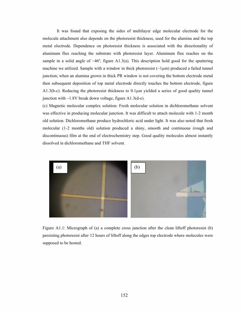
152
It was found that exposing the sides of multilayer edge molecular electrode for the
molecule attachment also depends on the photoresist thickness, used for the alumina and the top
metal electrode. Dependence on photoresist thickness is associated with the directionality of
aluminum flux reaching the substrate with photoresist layer. Aluminum flux reaches on the
sample in a solid angle of ~46º, figure A1.3(a). This description hold good for the sputtering
machine we utilized. Sample with a window in thick photoresist (~1µm) produced a failed tunnel
junction; when an alumina grown in thick PR window is not covering the bottom electrode metal
then subsequent deposition of top metal electrode directly touches the bottom electrode, figure
A1.3(b-c). Reducing the photoresist thickness to 0.1µm yielded a series of good quality tunnel
junction with ~1.8V break down voltage, figure A1.3(d-e).
(c) Magnetic molecular complex solution: Fresh molecular solution in dichloromethane solvent
was effective in producing molecular junction. It was difficult to attach molecule with 1-2 month
old solution. Dichloromethane produce hydrochloric acid under light. It was also noted that fresh
molecular (1-2 months old) solution produced a shiny, smooth and continuous (rough and
discontinuous) film at the end of electrochemistry step. Good quality molecules almost instantly
dissolved in dichloromethane and THF solvent.
Figure A1.1: Micrograph of (a) a complete cross junction after the clean liftoff photoresist (b)
persisting photoresist after 12 hours of liftoff along the edges top electrode where molecules were
supposed to be hosted.
(a) (b)

153
Figure A1.2: Step height measurement of alumina grown (a) with moderately eroded aluminum
target (b) with heavily eroded aluminum target. (c) Photoresist profile to be avoided.
(a)
(c)

154
Figure A1.3: Effect of directionality of Al plasma and photoresist thickness: (a) In the sputtering
chamber aluminum plasma hit the sample in a solid angle of ~46º degree (according to gun
geometry and sample position). (b) Aluminum plasma impinging in a 1-2 µm thick photoresist
window, (c) shadow effect of [L] photoresist wall avoiding the complete coverage of bottom
metal electrode, (d) deposition of the top electrode make direct contact with bottom electrode to
yield a failed tunnel junction. (e) 100-150nm thick photoresist wall allow aluminum plasma to
cover bottom electrode more uniformly, moderate shadow effect is still likely (f) top electrode
will not touch the bottom electrode.

155
Appendix A2
Stability of Bottom Metal Layers.
Multilayer edge molecular electrodes where cobalt metal was present in the bottom
electrode at numerous occasion damages were observed after the electrochemical molecule
treatment. We have carefully studied the damages to the junctions and their causes. There were
mainly two type of devices configuration, dots and cross junction pattern, were studied. It was
observed that when Co thickness was in higher side (7-12nm) damage to the bottom electrode
was severe. We worried if etching of dots and cross junction may produce the effect which we
found due to the molecules. Typical nature of damage to the dots and cross junction is showed in
figure A2.1, and figure A2.2.
In the present study mainly, NiFe, Co and Ta metals were utilized. Chemical etching
rates of the NiFe and Ta in the molecular cluster solution of dichloromethane solvent were too
small to determine. However, Cobalt has <2nm/min dissolution rate in the molecular solution (in
dichloromethane solvent). Cobalt also dissolves in regularly used MF-319 developer (~5nm/min).
A layer of Co (5-7nm) under a protecting layer of 3-5nm of NiFe showed excellent stability
against both, molecular solution in dichloromethane solvent and MF-319 developer. Aged
molecular solution was found to be more aggressive, presumably due to the build up of
hydrochloric acid getting produced from the light exposure of dichloromethane solvent. We
generally performed molecular attachment through two electrode electrochemistry. Metals pads
are found to be more aggressively attacked by the molecular solution in the vicinity of electrode
contact point on metal pads.
A number of control experiments were performed to obviate the doubt that etching or
material removal could cause the main findings (molecule induced magnetic ordering and current
suppression). Current suppression phenomenon was observed with a molecular solution in THF
solvent. Molecular solution in THF solvent was observed to be safe for the Co metal.
In some cases, it was found that multilayer got damaged near the edges. This observation
was seen with those samples for which no undercut developing treatment was employed and
over-exposure and over-developing conditions were used during photolithography; these
conditions does not produce abrupt photoresist edges. After the multilayer deposition and liftoff,
a photoresist layer is expected to persist. This photoresist layer undergo lift-off during
electrochemical molecular treatment with aggressive molecular solution.
Here we present a case study to distinguish the nature of damages to the multilayer edge
molecular electrodes from the lift-off of persisting thin PR under multilayer and from the
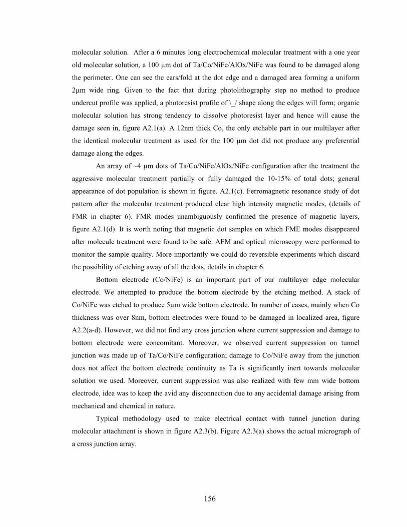
156
molecular solution. After a 6 minutes long electrochemical molecular treatment with a one year
old molecular solution, a 100 µm dot of Ta/Co/NiFe/AlOx/NiFe was found to be damaged along
the perimeter. One can see the ears/fold at the dot edge and a damaged area forming a uniform
2µm wide ring. Given to the fact that during photolithography step no method to produce
undercut profile was applied, a photoresist profile of \_/ shape along the edges will form; organic
molecular solution has strong tendency to dissolve photoresist layer and hence will cause the
damage seen in, figure A2.1(a). A 12nm thick Co, the only etchable part in our multilayer after
the identical molecular treatment as used for the 100 µm dot did not produce any preferential
damage along the edges.
An array of ~4 µm dots of Ta/Co/NiFe/AlOx/NiFe configuration after the treatment the
aggressive molecular treatment partially or fully damaged the 10-15% of total dots; general
appearance of dot population is shown in figure. A2.1(c). Ferromagnetic resonance study of dot
pattern after the molecular treatment produced clear high intensity magnetic modes, (details of
FMR in chapter 6). FMR modes unambiguously confirmed the presence of magnetic layers,
figure A2.1(d). It is worth noting that magnetic dot samples on which FME modes disappeared
after molecule treatment were found to be safe. AFM and optical microscopy were performed to
monitor the sample quality. More importantly we could do reversible experiments which discard
the possibility of etching away of all the dots, details in chapter 6.
Bottom electrode (Co/NiFe) is an important part of our multilayer edge molecular
electrode. We attempted to produce the bottom electrode by the etching method. A stack of
Co/NiFe was etched to produce 5µm wide bottom electrode. In number of cases, mainly when Co
thickness was over 8nm, bottom electrodes were found to be damaged in localized area, figure
A2.2(a-d). However, we did not find any cross junction where current suppression and damage to
bottom electrode were concomitant. Moreover, we observed current suppression on tunnel
junction was made up of Ta/Co/NiFe configuration; damage to Co/NiFe away from the junction
does not affect the bottom electrode continuity as Ta is significantly inert towards molecular
solution we used. Moreover, current suppression was also realized with few mm wide bottom
electrode, idea was to keep the avid any disconnection due to any accidental damage arising from
mechanical and chemical in nature.
Typical methodology used to make electrical contact with tunnel junction during
molecular attachment is shown in figure A2.3(b). Figure A2.3(a) shows the actual micrograph of
a cross junction array.
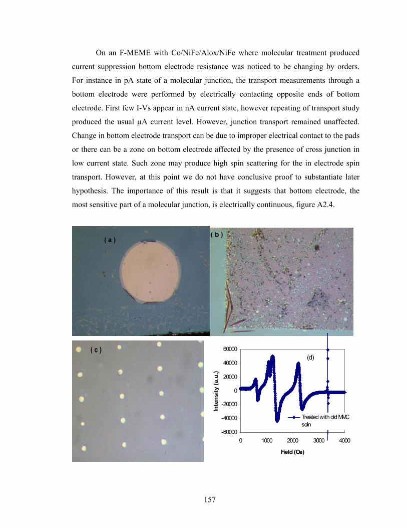
157
On an F-MEME with Co/NiFe/Alox/NiFe where molecular treatment produced
current suppression bottom electrode resistance was noticed to be changing by orders.
For instance in pA state of a molecular junction, the transport measurements through a
bottom electrode were performed by electrically contacting opposite ends of bottom
electrode. First few I-Vs appear in nA current state, however repeating of transport study
produced the usual µA current level. However, junction transport remained unaffected.
Change in bottom electrode transport can be due to improper electrical contact to the pads
or there can be a zone on bottom electrode affected by the presence of cross junction in
low current state. Such zone may produce high spin scattering for the in electrode spin
transport. However, at this point we do not have conclusive proof to substantiate later
hypothesis. The importance of this result is that it suggests that bottom electrode, the
most sensitive part of a molecular junction, is electrically continuous, figure A2.4.
-60000
-40000
-20000
0
20000
40000
60000
0 1000 2000 3000 4000
Field (Oe)
Inte
nsity
(a.u
.)
Treated with old MMCsoln
(d)

158
Figure A2.1: (a) ~2µm damage along perimeter of a 100µm Ta/Co/NiFe/AlOx/NiFe dot
after 6 min of electrochemical molecular treatment with 1 year old molecular solution, (b)
bare 12nm thick Cobalt after 20min of electrochemical treatment with same solution as
used in (a), (c) 4µm diameter Ta/Co/NiFe/AlOx/NiFe after exactly the same molecular
treatment as used in (a), (d) FMR spectra of dots shown in(c). (e) a cross junction whose
bottom electrode was prepared by the electrochemical etching of bottom electrode
(Co/NiFe).

159
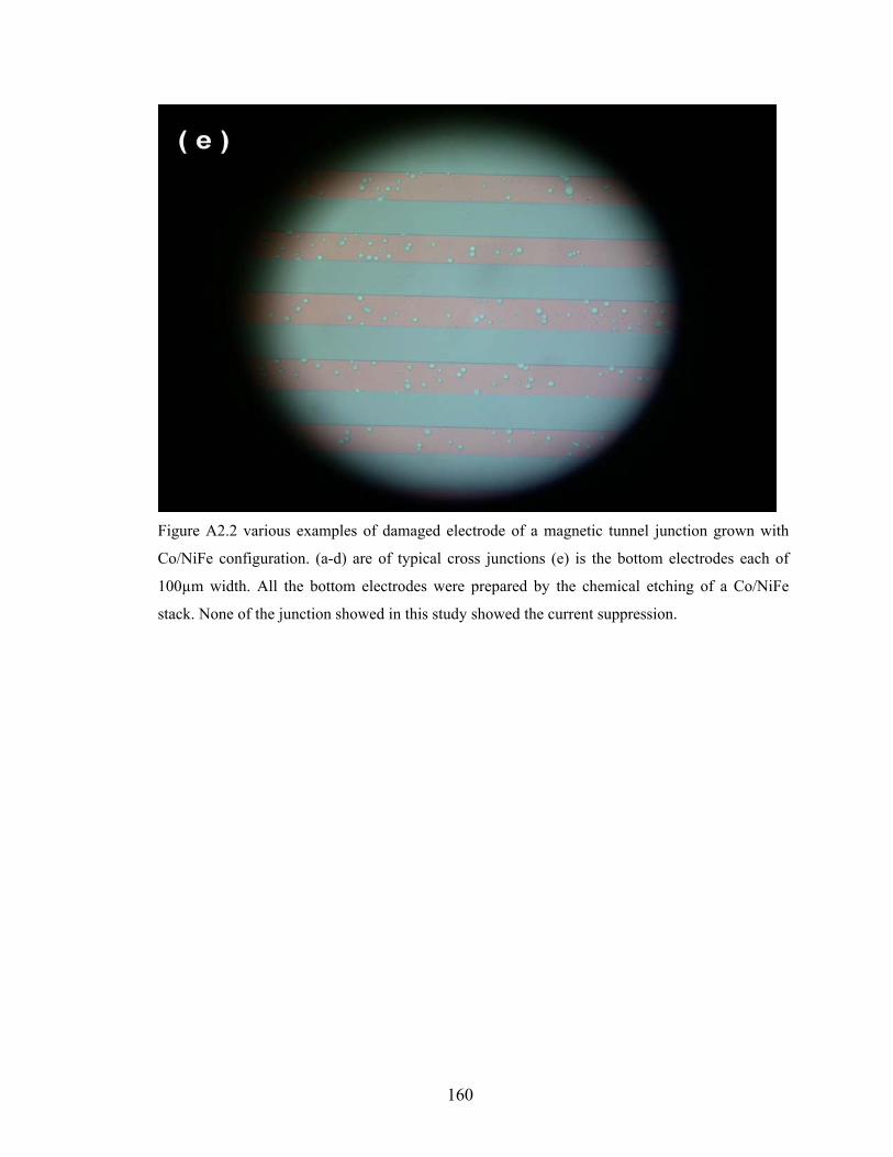
160
Figure A2.2 various examples of damaged electrode of a magnetic tunnel junction grown with
Co/NiFe configuration. (a-d) are of typical cross junctions (e) is the bottom electrodes each of
100µm width. All the bottom electrodes were prepared by the chemical etching of a Co/NiFe
stack. None of the junction showed in this study showed the current suppression.
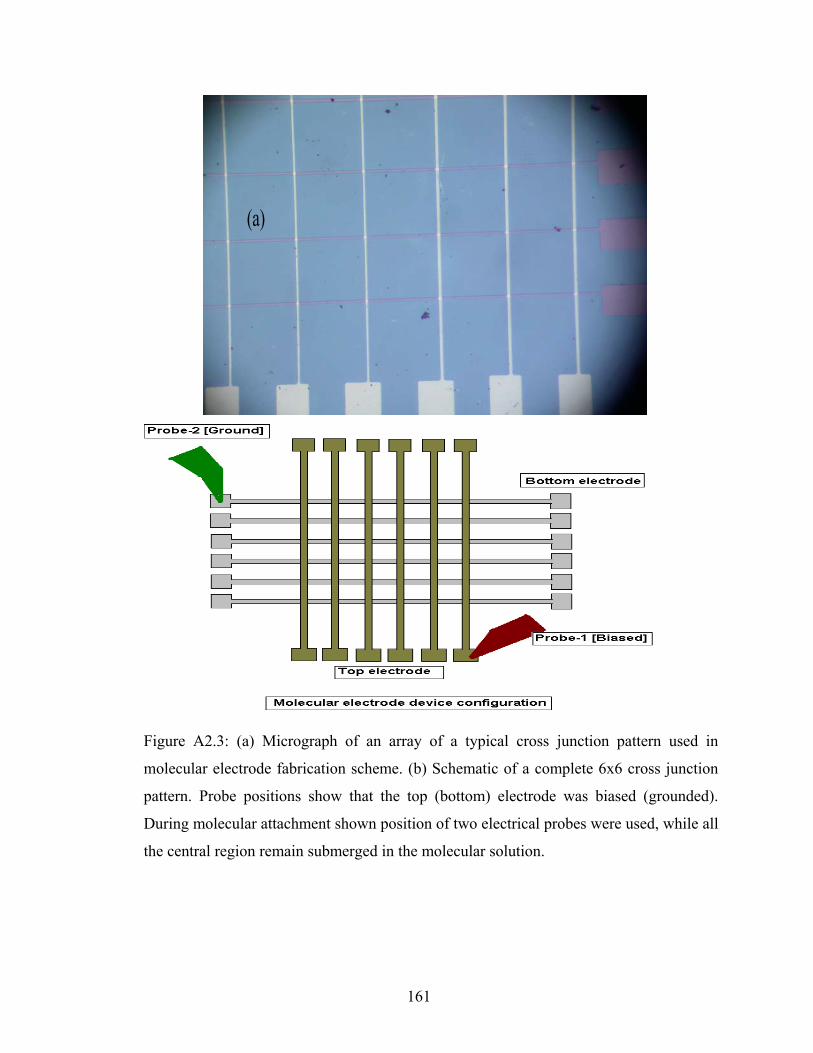
161
Figure A2.3: (a) Micrograph of an array of a typical cross junction pattern used in
molecular electrode fabrication scheme. (b) Schematic of a complete 6x6 cross junction
pattern. Probe positions show that the top (bottom) electrode was biased (grounded).
During molecular attachment shown position of two electrical probes were used, while all
the central region remain submerged in the molecular solution.
(a)
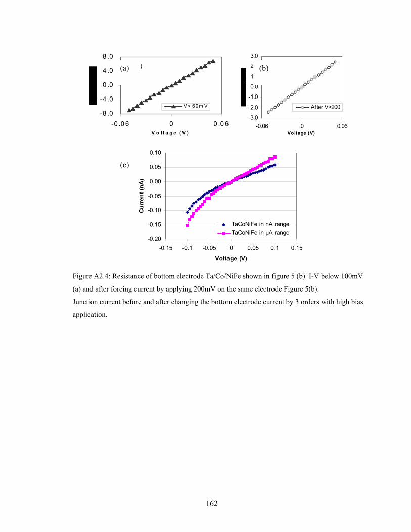
162
-8 .0
-4 .0
0 .0
4 .0
8 .0
-0 .0 6 0 0 .0 6V o l t a g e ( V )
V < 60m V
( h )
-3.0
-2.0
-1.0
0.0
1.0
2.0
3.0
-0.06 0 0.06Voltage (V)
After V>200
(i )
-0.20
-0.15
-0.10
-0.05
0.00
0.05
0.10
-0.15 -0.1 -0.05 0 0.05 0.1 0.15
Voltage (V)
Curr
ent (
nA)
TaCoNiFe in nA rangeTaCoNiFe in µA range
Figure A2.4: Resistance of bottom electrode Ta/Co/NiFe shown in figure 5 (b). I-V below 100mV
(a) and after forcing current by applying 200mV on the same electrode Figure 5(b).
Junction current before and after changing the bottom electrode current by 3 orders with high bias
application.
(a) (b)
(c)

163
Appendix A3
Fabrication of semiconductor-molecule-metal junction using multilayer edge molecular
electrode design
A Si/AlOx/NiFe based molecular junction was prepared. A p-type silicon wafer with 1-
50 Ω resistivity and thermally grown 100nm silicon di oxide was utilized. After defining a 5µm
window in photoresist, SiO2 was etched with BOE solution. Soon after etching of oxide samples
were put in vacuum for the deposition of AlOx and NiFe layer through a photoresist window,
across the silicon pattern. Deposition parameters used are same as mentioned in chapter 2. Lastly,
electrochemical molecule attachment was perfumed to produce silicon-molecule-metal junction.
Unambiguous increase in transport was noticed after the bridging of molecular channels. In order
to make electrical contact with silicon, electrical probes were directly touched to the opposite side
of AlOx/NiFe pattern.
Figure A3.1: Fabrication scheme (a) etch away a window in the SiO2 layer present over Si wafer.
(b) Deposit ~2nm alumina and NiFe metal electrode (c) attach molecules.
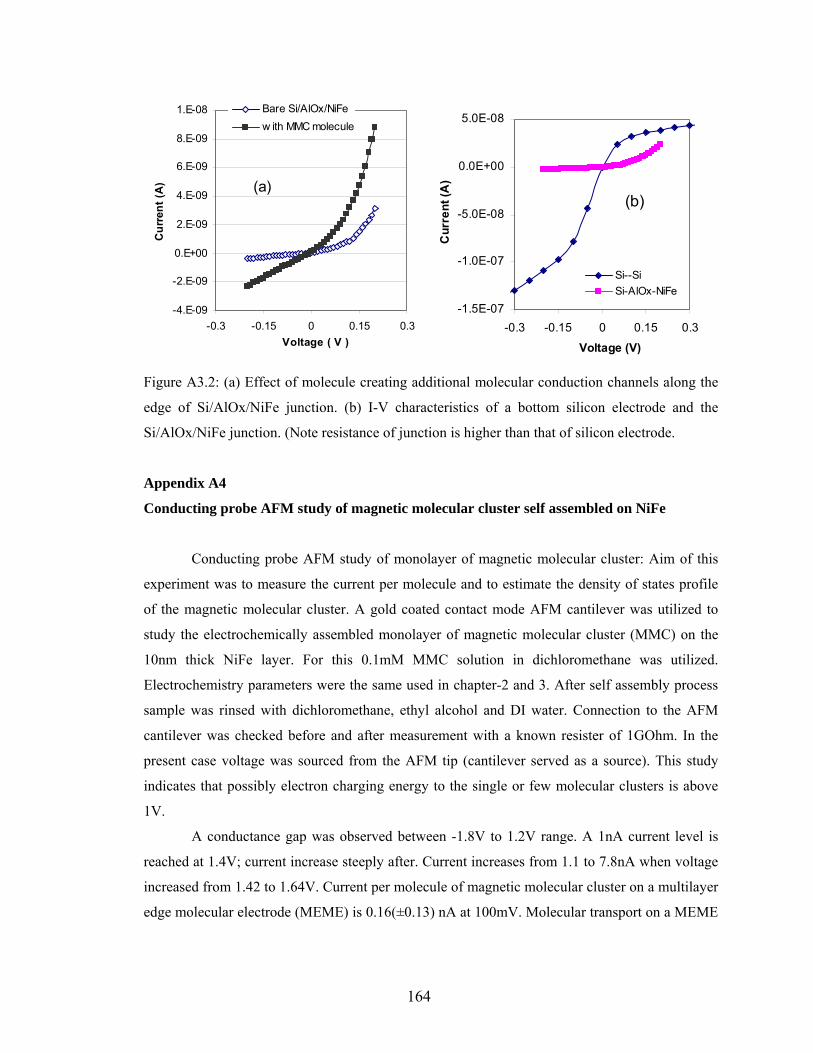
164
-4.E-09
-2.E-09
0.E+00
2.E-09
4.E-09
6.E-09
8.E-09
1.E-08
-0.3 -0.15 0 0.15 0.3Voltage ( V )
Cur
rent
(A)
Bare Si/AlOx/NiFew ith MMC molecule
(a)
-1.5E-07
-1.0E-07
-5.0E-08
0.0E+00
5.0E-08
-0.3 -0.15 0 0.15 0.3
Voltage (V)
Cur
rent
(A)
Si--SiSi-AlOx-NiFe
(b)
Figure A3.2: (a) Effect of molecule creating additional molecular conduction channels along the
edge of Si/AlOx/NiFe junction. (b) I-V characteristics of a bottom silicon electrode and the
Si/AlOx/NiFe junction. (Note resistance of junction is higher than that of silicon electrode.
Appendix A4
Conducting probe AFM study of magnetic molecular cluster self assembled on NiFe
Conducting probe AFM study of monolayer of magnetic molecular cluster: Aim of this
experiment was to measure the current per molecule and to estimate the density of states profile
of the magnetic molecular cluster. A gold coated contact mode AFM cantilever was utilized to
study the electrochemically assembled monolayer of magnetic molecular cluster (MMC) on the
10nm thick NiFe layer. For this 0.1mM MMC solution in dichloromethane was utilized.
Electrochemistry parameters were the same used in chapter-2 and 3. After self assembly process
sample was rinsed with dichloromethane, ethyl alcohol and DI water. Connection to the AFM
cantilever was checked before and after measurement with a known resister of 1GOhm. In the
present case voltage was sourced from the AFM tip (cantilever served as a source). This study
indicates that possibly electron charging energy to the single or few molecular clusters is above
1V.
A conductance gap was observed between -1.8V to 1.2V range. A 1nA current level is
reached at 1.4V; current increase steeply after. Current increases from 1.1 to 7.8nA when voltage
increased from 1.42 to 1.64V. Current per molecule of magnetic molecular cluster on a multilayer
edge molecular electrode (MEME) is 0.16(±0.13) nA at 100mV. Molecular transport on a MEME
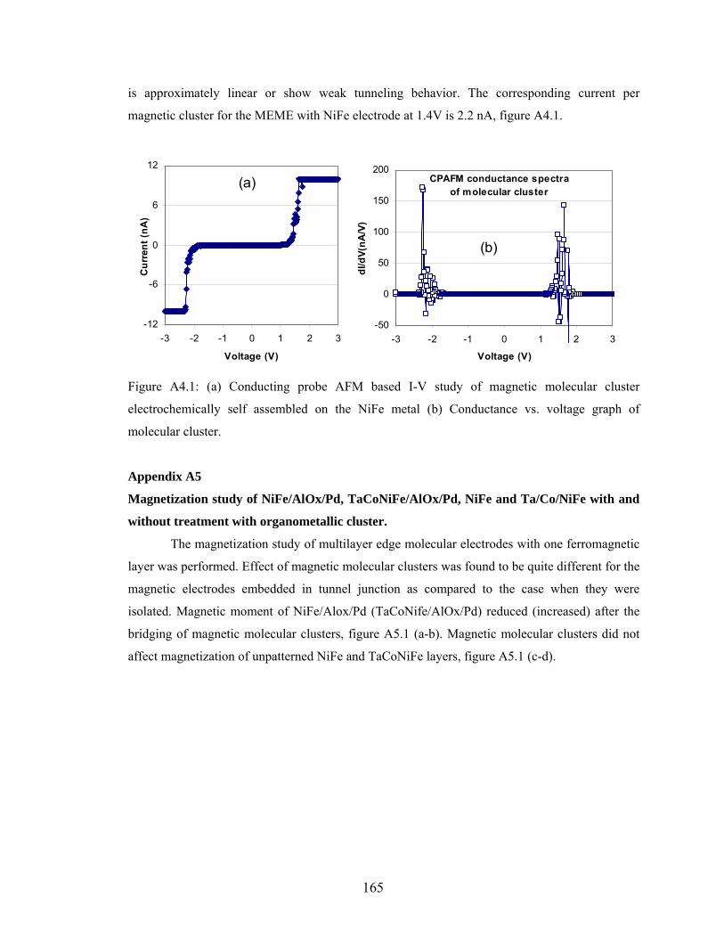
165
is approximately linear or show weak tunneling behavior. The corresponding current per
magnetic cluster for the MEME with NiFe electrode at 1.4V is 2.2 nA, figure A4.1.
-12
-6
0
6
12
-3 -2 -1 0 1 2 3
Voltage (V)
Cur
rent
(nA
)
(a) CPAFM conductance spectraof molecular cluster
-50
0
50
100
150
200
-3 -2 -1 0 1 2 3
Voltage (V)dI
/dV(
nA/V
)
(b)
Figure A4.1: (a) Conducting probe AFM based I-V study of magnetic molecular cluster
electrochemically self assembled on the NiFe metal (b) Conductance vs. voltage graph of
molecular cluster.
Appendix A5
Magnetization study of NiFe/AlOx/Pd, TaCoNiFe/AlOx/Pd, NiFe and Ta/Co/NiFe with and
without treatment with organometallic cluster.
The magnetization study of multilayer edge molecular electrodes with one ferromagnetic
layer was performed. Effect of magnetic molecular clusters was found to be quite different for the
magnetic electrodes embedded in tunnel junction as compared to the case when they were
isolated. Magnetic moment of NiFe/Alox/Pd (TaCoNife/AlOx/Pd) reduced (increased) after the
bridging of magnetic molecular clusters, figure A5.1 (a-b). Magnetic molecular clusters did not
affect magnetization of unpatterned NiFe and TaCoNiFe layers, figure A5.1 (c-d).
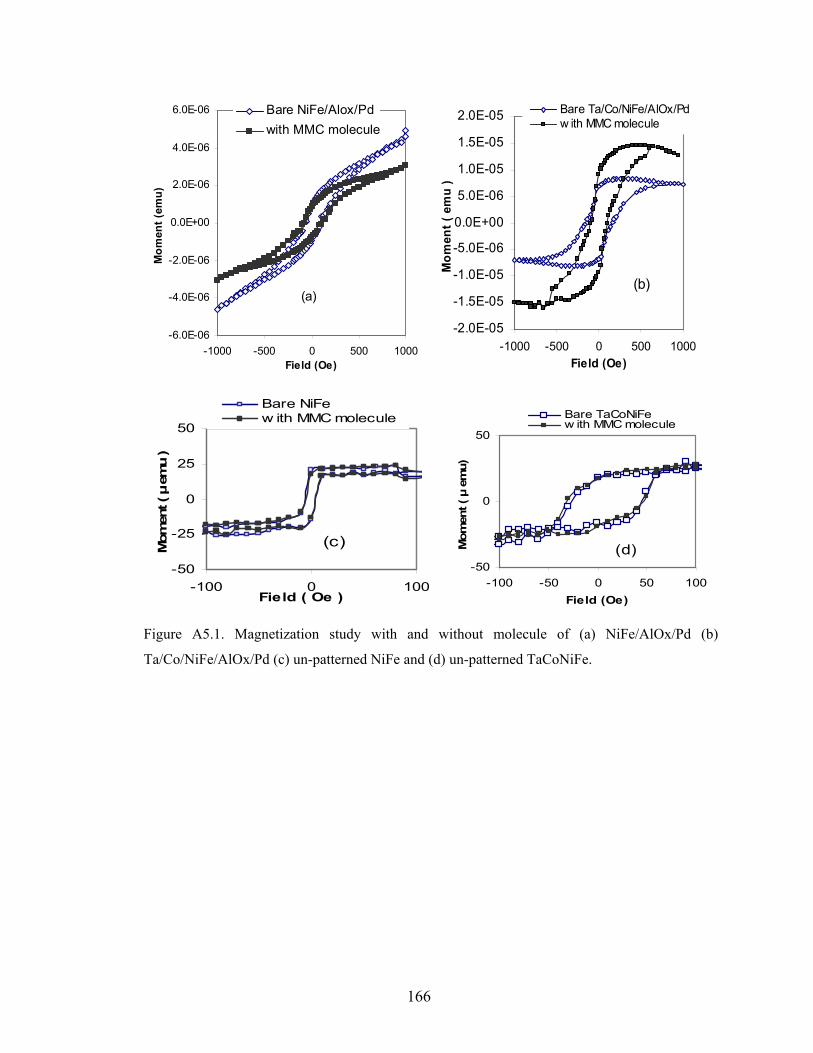
166
-6.0E-06
-4.0E-06
-2.0E-06
0.0E+00
2.0E-06
4.0E-06
6.0E-06
-1000 -500 0 500 1000Field (Oe)
Mom
ent (
emu)
Bare NiFe/Alox/Pdwith MMC molecule
(a)
-2.0E-05
-1.5E-05
-1.0E-05
-5.0E-06
0.0E+00
5.0E-06
1.0E-05
1.5E-05
2.0E-05
-1000 -500 0 500 1000Field (Oe)
Mom
ent (
em
u )
Bare Ta/Co/NiFe/AlOx/Pdw ith MMC molecule
(b)
-50
-25
0
25
50
-100 0 100Field ( Oe )
Mom
ent (
µ e
mu
)
Bare NiFew ith MMC molecule
(c)
-50
0
50
-100 -50 0 50 100Field (Oe)
Mom
ent (
μ e
mu)
Bare TaCoNiFew ith MMC molecule
(d)
Figure A5.1. Magnetization study with and without molecule of (a) NiFe/AlOx/Pd (b)
Ta/Co/NiFe/AlOx/Pd (c) un-patterned NiFe and (d) un-patterned TaCoNiFe.

167
Appendix A6
Molecular Spin Device with Different Configurations of Ferromagnetic Electrodes
Three configurations of ferromagnetic-multilayer edge molecular electrode were utilized
to form molecular spin devices. Three configurations are:
(a) NiFe(10nm)/AlOx(2nm)/NiFe(10nm)
(b) Ta(5nm)/Co(5nm)/NiFe(5nm)/AlOx(2nm)/NiFe(10nm)
(c) Ta(5nm)/Co(5nm)/NiFe(5nm)/AlOx(2nm)/NiFe(5nm)/Ta(5nm)
Magnetic measurements and transport behavior of the entire three configurations were found to
be quite distinct. Following are the details of representative behavior of each configuration.
FMR study show that NiFe(10nm)-AlOx(2nm)-NiFe(10nm) configuration showed two
resonance modes at 1126 and 1223 Oe. Smaller mode (optical mode) lying after taller mode
(acoustic mode) implies that nature of inter-layer coupling via alumina is antiferromagnetic,
figure 1(a). Resonance mode for single NiFe electrode of 10nm thickness appears at 1150Oe.
After the bridging of magnetic molecular clusters, current (at 100mV) of NiFe/Alox/NiFe
increased from 0.2µA to 3µA. Magnetization of this molecular electrode by the 0.45T, in-plane
magnetic field for 30min forced a low current state, 0.1µA at 100mV, figureA6.1(c). Repeating
I-V or leaving the device for sometime exhibited retrieval of high current state,
3.6µA at 100mV.
FMR spectra of Ta/Co/NiFe/AlOx/NiFe(Ta/Co/NiFe/AlOx/NiFe/Ta) contained higher
intensity peak (lower intensity peak) appear at lower magnetic field suggesting antiferromagnetic
(ferromagnetic coupling between two ferromagnetic layer, figure A6.2(a) and figure A6.2(b).
Bridging of MMC molecules on bare Ta/Co/NiFe/AlOx/NiFe(Ta/Co/NiFe/AlOx/NiFe/Ta)
reduces (increases) the magnetic moment, figure A6.2(d)( figure A6.2(c)). Two magnetization
studies suggest that the two configurations behave almost opposite to each other. In the transport
study, magnetic molecular cluster forced the current suppression on tunnel junctions with
Ta/Co/NiFe/AlOx/NiFe configuration (details in chapter7). When bridged between the two
ferromagnetic electrodes of the Ta/Co/NiFe/AlOx/NiFe/Ta, magnetic molecular cluster produced
several current levels. Although current level tended to settle at lower levels than the background
current, but molecular junctions did not settle to the same low current state, figure A6.3(a). With
this configuration magnetic field could be used to switch the device current state from one level
to another. One device, whose current level initially was at pA level, figure A6.3(d), shifted to µA
level with the repeating magneto resistance study, figure A6.3(c). A summary of various current
stages seen on the magnetic molecular junction is in, figure A6.3(e). Many time a current state

168
changed with just the repetition of the I-V/MR measurements. A low current state set by the
magnetic field could be perturbed by repeating I-Vs, as seen with the case of NiFe-AlOx-NiFe.
On another F-MEME with Ta/Co/NiFe/AlOx/NiFe/Ta configuration, prepared in
different batch application of permanent in-plane magnetic field at RT was found to switch the
device current from µA current level to pA current state, figure A6.4.
-100000
-50000
0
50000
100000
400 700 1000 1300 1600
Field (oe)
Inte
nsity
(a.u
)
Bare NiFe-AlOx-NiFew ith MMC
(a)
NiFe-AlOx-NiFe
-2.E-05
-2.E-05
-1.E-05
-5.E-06
0.E+00
5.E-06
1.E-05
2.E-05
2.E-05
-0.5 0 0.5V(V)
I(A)
BareWith molecule
(b)
-1.0E-06
-5.0E-07
0.0E+00
5.0E-07
1.0E-06
-0.4 -0.2 0 0.2 0.4V ( V )
I(A)
After inplane B=0.45T
(c)
-7-6.8-6.6-6.4-6.2
-6-5.8-5.6-5.4-5.2
-5 Bare
With M
olecule
Afterm
agnetization
After severalI-Vs
Log
[ I (A
) ]
At 100mV
(d)
Figure A6.1: (a) FMR response of NiFe/AlOx/NiFe, (b) I-V before after establishment of
molecular conduction channels (c) after 0.45T in plane magnetization molecular device settling
into two order smaller current (d) summary of current value at 100mV in various stages of
NiFe/AlOx/NiFe.

169
-30000
-20000
-10000
0
10000
20000
30000
400 600 800 1000 1200 1400 1600
Field ( Oe )
Inte
nsity
(a.u
)
Ta/Co/NiFe/AlOx/NiFe/Ta
(a)
-80000
-60000
-40000
-20000
0
20000
40000
60000
80000
400 600 800 1000 1200 1400 1600
Field(Oe)
Inte
nsity
(a.u
.)
Ta/Co/NiFe/AlOx/NiFe
(b)
-8.0E-05
-6.0E-05
-4.0E-05
-2.0E-05
0.0E+00
2.0E-05
4.0E-05
6.0E-05
8.0E-05
-4000 -2000 0 2000 4000
Field (Oe)
Mom
ent (
emu)
Bare Ta/Co/NiFe/AlOx/NiFe/Tawith MMC molecule
(c)
-1.5E-04
-1.0E-04
-5.0E-05
0.0E+00
5.0E-05
1.0E-04
1.5E-04
-5000 0 5000
Field (Oe)
Mom
ent (
emu)
Bare Ta/Co/NiFe/AlOx/NiFew ith MMC molecule
(d)
Figure A6.2. FMR response of bare TaCoNife/AlOx/NiFe/Ta (a) and Ta/Co/NiFe/AlOx/NiFe (b).
SQUID magnetic measurement of with and without molecule of TaCoNife/AlOx/NiFe/Ta (c) and
Ta/Co/NiFe/AlOx/NiFe (d).
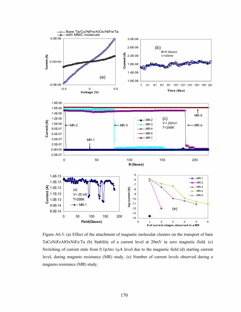
170
-5.0E-06
0.0E+00
5.0E-06
-0.5 0 0.5Voltage (V)
Cur
rent
(A)
Bare Ta/Co/NiFe/AlOx/NiFe/Tawith MMC molecule
(a)1.0E-08
1.4E-08
1.8E-08
2.2E-08
2.6E-08
3.0E-08
1 21 41 61 81 101 121 141 161 181 201
Time (Sec)
Cur
rem
t (A
)
(b) B=0 Gauss V=20mV
-2.0E-07
0.0E+00
2.0E-07
4.0E-07
6.0E-07
8.0E-071.0E-06
1.2E-06
1.4E-06
1.6E-06
1.8E-06
0 50 100 150 200B (Gauss)
Cur
rent
(A) MR-2
MR-3MR-4MR-5MR-1MR-1
MR-2 MR-3 MR-4
MR-5(c)V = 20mVT=298K
8.0E-149.0E-141.0E-131.1E-13
1.2E-131.3E-131.4E-13
0 50 100 150 200Field(Gauss)
Cur
rent
(A)
MR-1
(d)V= 20 mVT=298K
-14
-13
-12
-11
-10
-9
-8
-7
-6
-5
0 1 2 3 4 5 6# of current stages observed in a MR
log
(cur
rent
(A))
MR-1MR-2MR-3MR-4MR-5
(e)
Figure A6.3: (a) Effect of the attachment of magnetic molecular clusters on the transport of bare
TaCoNiFeAlOxNiFe/Ta (b) Stability of a current level at 20mV in zero magnetic field. (c)
Switching of current state from 0.1pAto 1µA level due to the magnetic field (d) starting current
level, during magneto resistance (MR) study. (e) Number of current levels observed during a
magneto resistance (MR) study.

171
-1.5E-05
-1.0E-05
-5.0E-06
0.0E+00
5.0E-06
1.0E-05
1.5E-05
-0.3 -0.2 -0.1 0 0.1 0.2 0.3
Voltage (V)
Cur
rent
bef
ore
mag
. (A
)
-6.0E-12
-4.0E-12
-2.0E-12
0.0E+00
2.0E-12
4.0E-12
6.0E-12
Cur
rent
aft
er m
ag. (
A)
Before magnetizationAfter Magnetization
Figure A6.4: Magnetic molecular cluster treated TaCo/NiFe/AlOx/NiFe/Ta before and after
magnetization by an in-plane 0.45T magnetic field at RT.
Appendix A7
Low Temperature Study of Magnetic Molecular Cluster Treated Ta/Co/NiFe/AlOx/NiFe
Ferromagnetic Multilayer Edge Molecular Electrodes (F-MEME)
A few F-MEMEs showed dramatic current suppression (of ~6 orders) after the bridging
of magnetic molecular clusters on the exposed edge. Three MMC treated F-MEME were
subjected to low temperature transport study up to 77K. Current of all the junctions settled into
pA state. However, I-V spectra were accompanied by the sharp peaks, figure A7.1(a-c). These
peaks appeared at various positions on voltage axis; peaks were found to occur more frequently at
few specific positions, e.g. 0.2V and 0.3V, figure A7.1(d). Highest number of spikes or peaks
was observed at 0.3V. According to our calculation molecular transport with MMC treated
Ta/AlOx/Ta exhibited ~0.3V activation energy, chapter 3. It is likely that 0.3V peak is arising
from a vibration mode or change in conformation at the core of the molecule. We are unable to
pinpoint the origin of 0.2V peak. It is quite likely that molecule assume several charge states
during an I-V. These peaks persisted after the warming of F-MEME sample up to room
temperature; intensity of peaks was found to be in nA range. However, these peaks were not
observed after the few hours at RT.
To minimize the role of noise, duration of each I-V was kept to be 1hour. I-V studies
were performed with Keithely-6430 sub femtoamp source meter equipped with preamplifier.
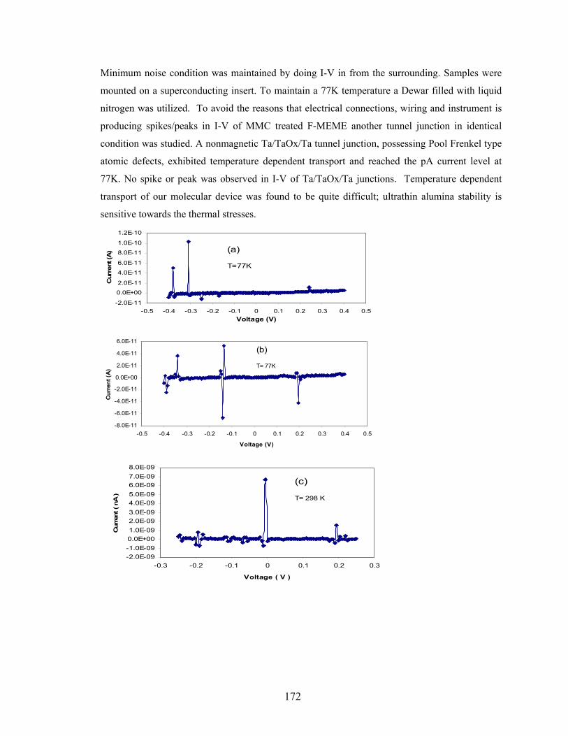
172
Minimum noise condition was maintained by doing I-V in from the surrounding. Samples were
mounted on a superconducting insert. To maintain a 77K temperature a Dewar filled with liquid
nitrogen was utilized. To avoid the reasons that electrical connections, wiring and instrument is
producing spikes/peaks in I-V of MMC treated F-MEME another tunnel junction in identical
condition was studied. A nonmagnetic Ta/TaOx/Ta tunnel junction, possessing Pool Frenkel type
atomic defects, exhibited temperature dependent transport and reached the pA current level at
77K. No spike or peak was observed in I-V of Ta/TaOx/Ta junctions. Temperature dependent
transport of our molecular device was found to be quite difficult; ultrathin alumina stability is
sensitive towards the thermal stresses.
-2.0E-11
0.0E+00
2.0E-11
4.0E-11
6.0E-11
8.0E-11
1.0E-10
1.2E-10
-0.5 -0.4 -0.3 -0.2 -0.1 0 0.1 0.2 0.3 0.4 0.5Voltage (V)
Cur
rent
(A) (a)
T=77K
-8.0E-11
-6.0E-11
-4.0E-11
-2.0E-11
0.0E+00
2.0E-11
4.0E-11
6.0E-11
-0.5 -0.4 -0.3 -0.2 -0.1 0 0.1 0.2 0.3 0.4 0.5
Voltage (V)
Cur
rent
(A)
(b)
T= 77K
-2.0E-09-1.0E-090.0E+001.0E-092.0E-093.0E-094.0E-095.0E-096.0E-097.0E-098.0E-09
-0.3 -0.2 -0.1 0 0.1 0.2 0.3
Voltage ( V )
Cur
rent
( nA
)
(c)
T= 298 K
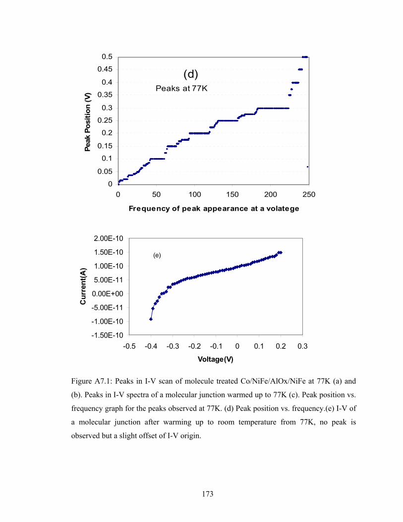
173
0
0.05
0.1
0.15
0.2
0.25
0.3
0.35
0.4
0.45
0.5
0 50 100 150 200 250
Frequency of peak appearance at a volatege
Peak
Pos
ition
(V)
(d)Peaks at 77K
-1.50E-10
-1.00E-10
-5.00E-11
0.00E+00
5.00E-11
1.00E-10
1.50E-10
2.00E-10
-0.5 -0.4 -0.3 -0.2 -0.1 0 0.1 0.2 0.3
Voltage(V)
Cur
rent
(A)
(e)
Figure A7.1: Peaks in I-V scan of molecule treated Co/NiFe/AlOx/NiFe at 77K (a) and
(b). Peaks in I-V spectra of a molecular junction warmed up to 77K (c). Peak position vs.
frequency graph for the peaks observed at 77K. (d) Peak position vs. frequency.(e) I-V of
a molecular junction after warming up to room temperature from 77K, no peak is
observed but a slight offset of I-V origin.

174
Appendix A8
Labview Programs for Transport and Magneto Resistance Studies
Source meter KE2430

175
Program for Magneto Resistance Study:

176
Source Meter KE6430: For Continuous I-V Studies
177
REFERENCES
1 I. Zutic, J. Fabian, and S. C. Erwin, "Bipolar spintronics: Fundamentals and
applications" Ibm Journal Of Research And Development 50, 121-139 (2006). 2 C. R. Barnes, "The proposed Cambrian-Ordovician global boundary stratotype and point
(GSSP) in Western Newfoundland, Canada" Geological Magazine 125, 381 (1988). 3 D. F. Li, S. Parkin, G. B. Wang, G. T. Yee, R. Clerac, W. Wernsdorfer, and S. M.
Holmes, "An S=6 cyanide-bridged octanuclear (Fe4Ni4II)-Ni-III complex that exhibits slow relaxation of the magnetization" Journal Of The American Chemical Society 128, 4214-4215 (2006).
4 C. Joachim, J. K. Gimzewski, and A. Aviram, "Electronics using hybrid-molecular and mono-molecular devices" Nature 408, 541-548 (2000).
5 R. L. Carroll and C. B. Gorman, "The genesis of molecular electronics" Angewandte Chemie-International Edition 41, 4379-4400 (2002).
6 A. Aviram and M. A. Ratner, "Molecular Rectifiers" Chemical Physics Letters 29, 277-283 (1974).
7 M. A. Reed, C. Zhou, C. J. Muller, T. P. Burgin, and J. M. Tour, "Conductance of a molecular junction" Science 278, 252-254 (1997).
8 A. J. Epstein, "Organic-based magnets: Opportunities in photoinduced magnetism, spintronics, fractal magnetism, and beyond" Mrs Bulletin 28, 492-499 (2003).
9 J. R. Heath and M. A. Ratner, "Molecular electronics" Physics Today 56, 43-49 (2003). 10 C. Joachim and M. A. Ratner, "Molecular wires: guiding the super-exchange interactions
electrodes between two electrodes" Nanotechnology 15, 1065-1075 (2004). 11 D. K. James and J. M. Tour, "Electrical measurements in molecular electronics"
Chemistry Of Materials 16, 4423-4435 (2004). 12 S. A. Wolf, D. D. Awschalom, R. A. Buhrman, J. M. Daughton, S. von Molnar, M. L.
Roukes, A. Y. Chtchelkanova, and D. M. Treger, "Spintronics: A spin-based electronics vision for the future" Science 294, 1488-1495 (2001).
13 A. N. Pasupathy, R. C. Bialczak, J. Martinek, J. E. Grose, L. A. K. Donev, P. L. McEuen, and D. C. Ralph, "The Kondo effect in the presence of ferromagnetism" Science 306, 86-89 (2004).
14 E. G. Petrov, I. S. Tolokh, and V. May, "Magnetic field control of an electron tunnel current through a molecular wire" Journal Of Chemical Physics 108, 4386-4396 (1998).
15 E. G. Emberly and G. Kirczenow, "Molecular spintronics: spin-dependent electron transport in molecular wires" Chemical Physics 281, 311-324 (2002).
16 J. R. Petta, S. K. Slater, and D. C. Ralph, "Spin-dependent transport in molecular tunnel junctions" Physical Review Letters 93 (2004).
17 J. S. Moodera, J. Nassar, and G. Mathon, "Spin-tunneling in ferromagnetic junctions" Annual Review Of Materials Science 29, 381-432 (1999).
18 S. Parkin, "Spin-polarized current in spin valves and magnetic tunnel junctions" Mrs Bulletin 31, 389-394 (2006).
19 A. R. Rocha, V. M. Garcia-Suarez, S. W. Bailey, C. J. Lambert, J. Ferrer, and S. Sanvito, "Towards molecular spintronics" Nature Materials 4, 335-339 (2005).
20 S. Sanvito and A. R. Rocha, "Molecular-spintronics: The art of driving spin through molecules" Journal Of Computational And Theoretical Nanoscience 3, 624-642 (2006).
21 E. Holmstrom, L. Nordstrom, L. Bergqvist, B. Skubic, B. Hjorvarsson, I. A. Abrikosov, P. Svedlindh, and O. Eriksson, "On the sharpness of the interfaces in metallic multilayers" Proceedings Of The National Academy Of Sciences Of The United States Of America 101, 4742-4745 (2004).

178
22 F. Meier, V. Cerletti, O. Gywat, D. Loss, and D. D. Awschalom, "Molecular spintronics: Coherent spin transfer in coupled quantum dots" Physical Review B 69 (2004).
23 J. P. Launay, "Long-distance intervalence electron transfer" Chemical Society Reviews 30, 386-397 (2001).
24 L. Cheng, J. P. Yang, Y. X. Yao, D. W. Price, S. M. Dirk, and J. M. Tour, "Comparative study of electrochemically directed assembly versus conventional self-assembly of thioacetyl-terminated oligo(phenylene ethynlyene)s on gold and platinum surface" Langmuir 20, 1335-1341 (2004).
25 E. Y. Tsymbal, O. N. Mryasov, and P. R. LeClair, "Spin-dependent tunnelling in magnetic tunnel junctions" Journal Of Physics-Condensed Matter 15, R109-R142 (2003).
26 W. J. M. Naber, S. Faez, and W. G. van der Wiel, "Organic spintronics" Journal Of Physics D-Applied Physics 40, R205-R228 (2007).
27 M. Ouyang and D. D. Awschalom, "Coherent spin transfer between molecularly bridged quantum dots" Science 301, 1074-1078 (2003).
28 M. Verdaguer, "Rational synthesis of molecular magnetic materials: a tribute to Olivier Kahn" Polyhedron 20, 1115-1128 (2001).
29 M. N. Leuenberger, F. Meier, and D. Loss, "Quantum spin dynamics in molecular magnets" Monatshefte Fur Chemie 134, 217-233 (2003).
30 E. G. Petrov, I. S. Tolokh, A. A. Demidenko, and V. V. Gorbach, "Electron-Transfer Properties Of Quantum Molecular Wires" Chemical Physics 193, 237-253 (1995).
31 J. Park, A. N. Pasupathy, J. I. Goldsmith, C. Chang, Y. Yaish, J. R. Petta, M. Rinkoski, J. P. Sethna, H. D. Abruna, P. L. McEuen, and D. C. Ralph, "Coulomb blockade and the Kondo effect in single-atom transistors" Nature 417, 722-725 (2002).
32 M. N. Leuenberger and E. R. Mucciolo, "Berry-phase oscillations of the kondo effect in single-molecule magnets" Physical Review Letters 97 (2006).
33 H. B. Heersche, Z. de Groot, J. A. Folk, H. S. J. van der Zant, C. Romeike, M. R. Wegewijs, L. Zobbi, D. Barreca, E. Tondello, and A. Cornia, "Electron transport through single Mn-12 molecular magnets" Physical Review Letters 96, 206861 (2006).
34 R. M. Metzger, "Unimolecular electrical rectifiers" Chemical Reviews 103, 3803-3834 (2003).
35 Y. Selzer and D. L. Allara, "Single-molecule electrical junctions" Annual Review Of Physical Chemistry 57, 593-623 (2006).
36 A. Nitzan, "Electron transmission through molecules and molecular interfaces" Annual Review Of Physical Chemistry 52, 681-750 (2001).
37 R. L. McCreery, "Molecular electronic junctions" Chemistry Of Materials 16, 4477-4496 (2004).
38 A. Nitzan and M. A. Ratner, "Electron transport in molecular wire junctions" Science 300, 1384-1389 (2003).
39 W. J. Liang, M. P. Shores, M. Bockrath, J. R. Long, and H. Park, "Kondo resonance in a single-molecule transistor" Nature 417, 725-729 (2002).
40 P. Tyagi, D. F. Li, S. M. Holmes, and B. J. Hinds, "Molecular Electrodes at the Exposed Edge of Metal-Insulator-Metal Trilayer Structures" Journal Of The American Chemical Society 129, 4923-4928 (2007).
41 J. C. Cuevas, J. Heurich, F. Pauly, W. Wenzel, and G. Schon, "Theoretical description of the electrical conduction in atomic and molecular junctions" Nanotechnology 14, R29-R38 (2003).
42 A. Salomon, D. Cahen, S. Lindsay, J. Tomfohr, V. B. Engelkes, and C. D. Frisbie, "Comparison of electronic transport measurements on organic molecules" Advanced Materials 15, 1881-1890 (2003).

179
43 L. Senapati, R. Pati, and S. C. Erwin, "Controlling spin-polarized electron transport through a molecule: The role of molecular conformation" Physical Review B (Condensed Matter and Materials Physics) 76, 024438 (2007).
44 M. Dorogi, J. Gomez, R. Osifchin, R. P. Andres, and R. Reifenberger, "Room-Temperature Coulomb-Blockade From A Self-Assembled Molecular Nanostructure" Physical Review B 52, 9071-9077 (1995).
45 A. D. Zhao, Q. X. Li, L. Chen, H. J. Xiang, W. H. Wang, S. Pan, B. Wang, X. D. Xiao, J. L. Yang, J. G. Hou, and Q. S. Zhu, "Controlling the Kondo effect of an adsorbed magnetic ion through its chemical bonding" Science 309, 1542-1544 (2005).
46 P. Seneor, A. Bernand-Mantel, and F. Petroff, "Nanospintronics: when spintronics meets single electron physics" Journal Of Physics-Condensed Matter 19 (2007).
47 H. J. Davies, "The Physics of Low Dimensional Semiconductors" Cambridge University Press (1998).
48 Y. Q. Xue and M. A. Ratner, "Theoretical principles of single-molecule electronics: A chemical and mesoscopic view" International Journal Of Quantum Chemistry 102, 911-924 (2005).
49 C. Joachim and M. A. Ratner, "Molecular electronics: Some views on transport junctions and beyond" Proceedings Of The National Academy Of Sciences Of The United States Of America 102, 8801-8808 (2005).
50 J. G. Simmons, "Generalized Formula For Electric Tunnel Effect Between Similar Electrodes Separated By A Thin Insulating Film" Journal Of Applied Physics 34, 1793-& (1963).
51 W. Y. Wang, T. Lee, and M. A. Reed, "Mechanism of electron conduction in self-assembled alkanethiol monolayer devices" Physical Review B 68 (2003).
52 G. V. Nazin, S. W. Wu, and W. Ho, "Tunneling rates in electron transport through double-barrier molecular junctions in a scanning tunneling microscope" Proceedings Of The National Academy Of Sciences Of The United States Of America 102, 8832-8837 (2005).
53 Y. Selzer, L. T. Cai, M. A. Cabassi, Y. X. Yao, J. M. Tour, T. S. Mayer, and D. L. Allara, "Effect of local environment on molecular conduction: Isolated molecule versus self-assembled monolayer" Nano Letters 5, 61-65 (2005).
54 X. Y. Zhu, "Charge transport at metal-molecule interfaces: A spectroscopic view" Journal Of Physical Chemistry B 108, 8778-8793 (2004).
55 S. Datta, "Electrical resistance: an atomistic view" Nanotechnology 15, S433-S451 (2004).
56 J. Martinek, M. Sindel, L. Borda, J. Barnas, J. Konig, G. Schon, and J. von Delft, "Kondo effect in the presence of itinerant-electron ferromagnetism studied with the numerical renormalization group method" Physical Review Letters 91 (2003).
57 S. W. Wu, G. V. Nazin, X. Chen, X. H. Qiu, and W. Ho, "Control of relative tunneling rates in single molecule bipolar electron transport" Physical Review Letters 93 (2004).
58 N. P. Guisinger, M. E. Greene, R. Basu, A. S. Baluch, and M. C. Hersam, "Room Temperature Negative Differential Resistance through Individual Organic Molecules on Silicon Surfaces" Nano Lett. 4, 55-59 (2004).
59 D. V. Averin, A. N. Korotkov, and K. K. Likharev, "Theory Of Single-Electron Charging Of Quantum-Wells And Dots" Physical Review B 44, 6199-6211 (1991).
60 D. Segal, A. Nitzan, W. B. Davis, M. R. Wasielewski, and M. A. Ratner, "Electron transfer rates in bridged molecular systems 2. A steady-state analysis of coherent tunneling and thermal transitions" Journal Of Physical Chemistry B 104, 3817-3829 (2000).
61 J. M. Seminario, C. E. De La Cruz, and P. A. Derosa, "A Theoretical Analysis of Metal-Molecule Contacts" J. Am. Chem. Soc. 123, 5616-5617 (2001).

180
62 R. H. M. Smit, Y. Noat, C. Untiedt, N. D. Lang, M. C. van Hemert, and J. M. van Ruitenbeek, "Measurement of the conductance of a hydrogen molecule" Nature 419, 906-909 (2002).
63 N. Nilius, T. M. Wallis, and W. Ho, "Localized molecular constraint on electron delocalization in a metallic chain" Physical Review Letters 90 (2003).
64 B. Q. Q. Xu, X. L. L. Li, X. Y. Y. Xiao, H. Sakaguchi, and N. J. J. Tao, "Electromechanical and conductance switching properties of single oligothiophene molecules" Nano Letters 5, 1491-1495 (2005).
65 B. Q. Xu and N. J. J. Tao, "Measurement of single-molecule resistance by repeated formation of molecular junctions" Science 301, 1221-1223 (2003).
66 X. Y. Xiao, B. Q. Xu, and N. J. Tao, "Measurement of single molecule conductance: Benzenedithiol and benzenedimethanethiol" Nano Letters 4, 267-271 (2004).
67 M. Mayor, H. B. Weber, J. Reichert, M. Elbing, C. von Hanisch, D. Beckmann, and M. Fischer, "Electric current through a molecular rod - Relevance of the position of the anchor groups" Angewandte Chemie-International Edition 42, 5834-5838 (2003).
68 J. Reichert, R. Ochs, D. Beckmann, H. B. Weber, M. Mayor, and H. von Lohneysen, "Driving current through single organic molecules" Physical Review Letters 88 (2002).
69 S. Kubatkin, A. Danilov, M. Hjort, J. Cornil, J. L. Bredas, N. Stuhr-Hansen, P. Hedegard, and T. Bjornholm, "Single-electron transistor of a single organic molecule with access to several redox states" Nature 425, 698-701 (2003).
70 W. F. Brinkman, R. C. Dynes, and J. M. Rowell, "Tunneling Conductance of Asymmetrical Barriers" Journal of Applied Physics 41, 1915-1921 (1970).
71 N. B. Zhitenev, H. Meng, and Z. Bao, "Conductance of small molecular junctions" Physical Review Letters 88 (2002).
72 H. Park, J. Park, A. K. L. Lim, E. H. Anderson, A. P. Alivisatos, and P. L. McEuen, "Nanomechanical oscillations in a single-C-60 transistor" Nature 407, 57-60 (2000).
73 A. N. Pasupathy, J. Park, C. Chang, A. V. Soldatov, S. Lebedkin, R. C. Bialczak, J. E. Grose, L. A. K. Donev, J. P. Sethna, D. C. Ralph, and P. L. McEuen, "Vibration-assisted electron tunneling in C-140 transistors" Nano Letters 5, 203-207 (2005).
74 L. H. Yu, Z. K. Keane, J. W. Ciszek, L. Cheng, M. P. Stewart, J. M. Tour, and D. Natelson, "Inelastic electron tunneling via molecular vibrations in single-molecule transistors" Physical Review Letters 93 (2004).
75 B. C. Stipe, M. A. Rezaei, and W. Ho, "Single-molecule vibrational spectroscopy and microscopy" Science 280, 1732-1735 (1998).
76 M. Turek and K. A. Matveev, "Cotunneling thermopower of single electron transistors" Physical Review B 65 (2002).
77 A. Nitzan, J. Jortner, J. Wilkie, A. L. Burin, and M. A. Ratner, "Tunneling time for electron transfer reactions" Journal Of Physical Chemistry B 104, 5661-5665 (2000).
78 M. Julliere, "Tunneling Between Ferromagnetic-Films" Physics Letters A 54, 225-226 (1975).
79 A. Iovan, S. Andersson, Y. G. Naidyuk, A. Vedyaev, B. Dieny, and V. Korenivski, "Spin Diode Based on Fe/MgO Double Tunnel Junction" Nano Lett. (2008).
80 P. M. Tedrow and R. Meservey, "Spin-Dependent Tunneling Into Ferromagnetic Nickel" Physical Review Letters 26, 192-& (1971).
81 S. Takahashi and S. Maekawa, "Effect of Coulomb blockade on magnetoresistance in ferromagnetic tunnel junctions" Physical Review Letters 80, 1758-1761 (1998).
82 H. C. Nam, H. Shim, S. K. Kim, and K. B. Cho, "Thickness Dependence of Magnetic Coupling Strength and Thermal Stability in a Spin-Dependent Tunnel Junction " Phys. Stat. Sol. (a) 201, 1708-1711 (2004).
83 M. Bode, M. Getzlaff, and R. Wiesendanger, "Spin-polarized vacuum tunneling into the exchange-split surface state of Gd(0001)" Physical Review Letters 81, 4256-4259 (1998).
181
84 E. Y. Tsymbal, Oleinik, II, and D. G. Pettifor, "Oxygen-induced positive spin polarization from Fe into the vacuum barrier" Journal Of Applied Physics 87, 5230-5232 (2000).
85 P. Crespo, R. Litran, T. C. Rojas, M. Multigner, J. M. de la Fuente, J. C. Sanchez-Lopez, M. A. Garcia, A. Hernando, S. Penades, and A. Fernandez, "Permanent magnetism, magnetic anisotropy, and hysteresis of thiol-capped gold nanoparticles" Physical Review Letters 93, 087204 (2004).
86 L. H. Yu and D. Natelson, "Transport in single-molecule transistors: Kondo physics and negative differential resistance" Nanotechnology 15, S517-S524 (2004).
87 M. R. Buitelaar, T. Nussbaumer, and C. Schonenberger, "Quantum dot in the Kondo regime coupled to superconductors" Physical Review Letters 89 (2002).
88 M. S. Choi, D. Sanchez, and R. Lopez, "Kondo effect in a quantum dot coupled to ferromagnetic leads: A numerical renormalization group analysis" Physical Review Letters 92 (2004).
89 S. Doniach, "Kondo Lattice And Weak Antiferromagnetism" Physica B & C 91, 231-234 (1977).
90 L. H. Yu and D. Natelson, "The Kondo effect in C-60 single-molecule transistors" Nano Letters 4, 79-83 (2004).
91 R. Cohen, K. Stokbro, J. M. L. Martin, and M. A. Ratner, "Charge transport in conjugated aromatic molecular junctions: Molecular conjugation and molecule-electrode coupling" Journal Of Physical Chemistry C 111, 14893-14902 (2007).
92 J. Martinek, Y. Utsumi, H. Imamura, J. Barnas, S. Maekawa, J. Konig, and G. Schon, "Kondo effect in quantum dots coupled to ferromagnetic leads" Physical Review Letters 91 (2003).
93 D. Goldhaber-Gordon, H. Shtrikman, D. Mahalu, D. Abusch-Magder, U. Meirav, and M. A. Kastner, "Kondo effect in a single-electron transistor" Nature 391, 156-159 (1998).
94 J. C. Slonczewski, "Conductance and exchange coupling of two ferromagnets separated by a tunneling barrier" Physical Review B 39, 6995 (1989).
95 M. Y. Zhuravlev, E. Y. Tsymbal, and A. V. Vedyayev, "Impurity-assisted interlayer exchange coupling across a tunnel barrier" Physical Review Letters 94 (2005).
96 W. Wetzels, G. E. W. Bauer, and M. Grifoni, "Exchange effects on electron transport through single-electron spin-valve transistors" Physical Review B 74 (2006).
97 A. Hubsch, J. C. Lin, J. Pan, and D. L. Cox, "Correlated hybridization in transition-metal complexes" Physical Review Letters 96 (2006).
98 H. Shimada, K. Ono, and Y. Ootuka, "Driving the Single Electron device with a Magnetic Field" J. App. Phys. 93, 8259 (2000).
99 M. Sindel, L. Borda, J. Martinek, R. Bulla, J. Konig, G. Schon, S. Maekawa, and J. von Delft, "Kondo quantum dot coupled to ferromagnetic leads: Numerical renormalization group study" Physical Review B 76 (2007).
100 J. J. Henderson, C. M. Ramsey, E. del Barco, A. Mishra, and G. Christou, "Fabrication of nanogapped single-electron transistors for transport studies of individual single-molecule magnets" Journal Of Applied Physics 101, 09E102 (2007).
101 M. H. Jo, J. E. Grose, K. Baheti, M. M. Deshmukh, J. J. Sokol, E. M. Rumberger, D. N. Hendrickson, J. R. Long, H. Park, and D. C. Ralph, "Signatures of molecular magnetism in single-molecule transport spectroscopy" Nano Letters 6, 2014-2020 (2006).
102 S. Voss, M. Fonin, U. Rudiger, M. Burgert, and U. Groth, "Experimental observation of a band gap in individual Mn-12 molecules on Au(111)" Applied Physics Letters 90, 133104 (2007).
103 A. A. Houck, J. Labaziewicz, E. K. Chan, J. A. Folk, and I. L. Chuang, "Kondo effect in electromigrated gold break junctions" Nano Letters 5, 1685-1688 (2005).

182
104 Y. Luo, C. P. Collier, J. O. Jeppesen, K. A. Nielsen, E. Delonno, G. Ho, J. Perkins, H. R. Tseng, T. Yamamoto, J. F. Stoddart, and J. R. Heath, "Two-dimensional molecular electronics circuits" Chemphyschem 3, 519-+ (2002).
105 M. A. Reed and J. M. Tour, "Computing with molecules" Scientific American 282, 86-93 (2000).
106 M. Galperin, A. Nitzan, S. Sek, and M. Majda, "Asymmetric electron transmission across asymmetric alkanethiol bilayer junctions" Journal Of Electroanalytical Chemistry 550, 337-350 (2003).
107 X. D. Cui, A. Primak, X. Zarate, J. Tomfohr, O. F. Sankey, A. L. Moore, T. A. Moore, D. Gust, L. A. Nagahara, and S. M. Lindsay, "Changes in the electronic properties of a molecule when it is wired into a circuit" Journal Of Physical Chemistry B 106, 8609-8614 (2002).
108 D. J. Wold and C. D. Frisbie, "Fabrication and characterization of metal-molecule-metal junctions by conducting probe atomic force microscopy" Journal Of The American Chemical Society 123, 5549-5556 (2001).
109 P. Tyagi, D. F. Li, S. M. Holmes, and B. J. Hinds, "Molecular electrodes at the exposed edge of metal/insulator/metal trilayer structures" Journal Of The American Chemical Society 129, 4929-4938 (2007).
110 S. W. Howell, S. M. Dirk, K. Childs, H. Pang, M. Blain, R. J. Simonson, J. M. Tour, and D. R. Wheeler, "Mass-fabricated one-dimensional silicon nanogaps for hybrid organic/nanoparticle arrays" Nanotechnology 16, 754-758 (2005).
111 G. J. Ashwell, P. Wierzchowiec, C. J. Bartlett, and P. D. Buckle, "Molecular electronics: connection across nano-sized electrode gaps" Chemical Communications, 1254-1256 (2007).
112 P. H. Townsend and T. A. Brunner, "Elastic Relationships In Layered Composite Media With Approximation For The Case Of Thin-Films On A Thick Substrate" Journal Of Applied Physics 62, 4438-4444 (1987).
113 D. R. Franca and A. Blouin, "All-optical measurement of in-plane and out-of-plane Young's modulus and Poisson's ratio in silicon wafers by means of vibration modes" Measurement Science & Technology 15, 859-868 (2004).
114 W. Bruckner, S. Baunack, M. Hecker, J. Thomas, S. Groudeva-Zotova, and C. M. Schneider, "Oxidation of NiFe(20 wt.%) thin films" Materials Science And Engineering B-Solid State Materials For Advanced Technology 86, 272-275 (2001).
115 Y. S. Song, S. J. Park, T. W. Kim, and C. W. Chung, "Influence of wet chemical cleaning on properties of magnetic tunnel junction stack for magnetic RAM" Electrochemical And Solid State Letters 7, C64-C66 (2004).
116 P. Tyagi, D. F. Li, S. M. Holmes, and B. J. Hinds, "Molecular Electrodes at the Exposed Edge of Metal/Insulator/Metal Trilayer Structures" Journal Of The American Chemical Society 129, 4929-4928 (2007).
117 C. E. Inman, S. M. Reed, and J. E. Hutchison, "In situ deprotection and assembly of S-tritylalkanethiols on gold yields monolayers comparable to those prepared directly from alkanethiols" Langmuir 20, 9144-9150 (2004).
118 Z. Mekhalif, F. Laffineur, N. Couturier, and J. Delhalle, "Elaboration of self-assembled monolayers of n-alkanethiols on nickel polycrystalline substrates: time, concentration, and solvent effects" Langmuir 19, 637-645 (2003).
119 W. Oepts, H. J. Verhagen, R. Coehoorn, and W. J. M. de Jonge, "Analysis of breakdown in ferromagnetic tunnel junctions" Journal Of Applied Physics 86, 3863-3872 (1999).
120 H. Li, J. L. Sun, and L. P. Huang, "Effects of ductile cobalt on fracture behavior of Al2O3-TiC ceramic" Materials Science And Engineering A-Structural Materials Properties Microstructure And Processing 323, 17-20 (2002).

183
121 T. L. Anderson, "Fracture Mechanics: Fundamental and Applications" Fracture Mechanics: Fundamental and Applications (CRC Press Boston) (1995).
122 R. F. Egerton, P. Li, and M. Malac, "Radiation damage in the TEM and SEM" Micron 35, 399-409 (2004).
123 C. Herring and J. K. Galt, "Elastic And Plastic Properties Of Very Small Metal Specimens" Physical Review 85, 1060-1061 (1952).
124 D. Kim, B. Heiland, W. D. Nix, E. Arzt, M. D. Deal, and J. D. Plummer, "Microstructure of thermal hillocks on blanket Al thin films" Thin Solid Films 371, 278-282 (2000).
125 K. S. Yoon, J. H. Park, J. H. Choi, J. Y. Yang, C. H. Lee, C. O. Kim, J. P. Hong, and T. W. Kang, "Performance of Co/Al2O3/NiFe magnetic tunnel junctions prepared by a two-step rf plasma oxidation method" Applied Physics Letters 79, 1160-1162 (2001).
126 J. Chen, M. A. Reed, A. M. Rawlett, and J. M. Tour, "Large on-off ratios and negative differential resistance in a molecular electronic device" Science 286, 1550-1552 (1999).
127 C. P. Collier, E. W. Wong, M. Belohradsky, F. M. Raymo, J. F. Stoddart, P. J. Kuekes, R. S. Williams, and J. R. Heath, "Electronically configurable molecular-based logic gates" Science 285, 391-394 (1999).
128 J. K. N. Mbindyo, T. E. Mallouk, J. B. Mattzela, I. Kratochvilova, B. Razavi, T. N. Jackson, and T. S. Mayer, "Template synthesis of metal nanowires containing monolayer molecular junctions" Journal Of The American Chemical Society 124, 4020-4026 (2002).
129 D. I. Gittins, D. Bethell, D. J. Schiffrin, and R. J. Nichols, "A nanometre-scale electronic switch consisting of a metal cluster and redox-addressable groups" Nature 408, 67-69 (2000).
130 R. Beckman, E. Johnston-Halperin, Y. Luo, J. E. Green, and J. R. Heath, "Bridging dimensions: Demultiplexing ultrahigh-density nanowire circuits" Science 310, 465-468 (2005).
131 N. A. Melosh, A. Boukai, F. Diana, B. Gerardot, A. Badolato, P. M. Petroff, and J. R. Heath, "Ultrahigh-density nanowire lattices and circuits" Science 300, 112-115 (2003).
132 H. Gossner, F. Wittmann, I. Eisele, T. Grabolla, and D. Behammer, "Vertical Mos Technology With Sub-0.1-Mu-M Channel Lengths" Electronics Letters 31, 1394-1396 (1995).
133 L. D. Qin, S. Park, L. Huang, and C. A. Mirkin, "On-wire lithography" Science 309, 113-115 (2005).
134 J. Berg, P. Lundgren, P. Enoksson, and S. Bengtsson, "Low frequency noise in silicon nanogaps" Applied Physics Letters 87 (2005).
135 S. M. Dirk, S. W. Howell, S. Zmuda, K. Childs, M. Blain, R. J. Simonson, and D. R. Wheeler, "Novel one-dimensional nanogap created with standard optical lithography and evaporation procedures" Nanotechnology 16, 1983-1985 (2005).
136 F. Maya, A. K. Flatt, M. P. Stewart, D. E. Shen, and J. M. Tour, "Formation and analysis of self-assembled monolayers from U-shaped oligo(phenylene ethynylene)s as candidates for molecular electronics" Chemistry Of Materials 16, 2987-2997 (2004).
137 H. B. Akkerman, P. W. M. Blom, D. M. de Leeuw, and B. de Boer, "Towards molecular electronics with large-area molecular junctions" Nature 441, 69-72 (2006).
138 D. M. Jeon, J. W. Park, D. H. Lee, S. Y. Yoon, D. H. Yoon, and S. J. Suh, "Annealing effect on the barrier properties and TMR of magnetic tunneling junctions fabricated in various oxidation conditions" Journal Of Magnetism And Magnetic Materials 272-76, 1956-1958 (2004).
139 D. R. Lide, 79 ed., edited by D. R. Lide (1998-1999). 140 C. M. Ruan, T. Bayer, S. Meth, and C. N. Sukenik, "Creation and characterization of n-
alkylthiol and n-alkylamine self-assembled monolayers on 316L stainless steel" Thin Solid Films 419, 95-104 (2002).

184
141 J. S. Moodera, X. Hao, G. A. Gibson, and R. Meservey, "Electron-Spin Polarization In Tunnel-Junctions In Zero Applied Field With Ferromagnetic Eus Barriers" Physical Review Letters 61, 637-640 (1988).
142 B. Ricco and M. Y. Azbel, "Physics Of Resonant Tunneling - The One-Dimensional Double-Barrier Case" Physical Review B 29, 1970-1981 (1984).
143 M. Di Ventra, S. T. Pantelides, and N. D. Lang, "The benzene molecule as a molecular resonant-tunneling transistor" Applied Physics Letters 76, 3448-3450 (2000).
144 F. Anariba and R. L. McCreery, "Electronic conductance behavior of carbon-based molecular junctions with conjugated structures" Journal Of Physical Chemistry B 106, 10355-10362 (2002).
145 S. Piccinin, A. Selloni, S. Scandolo, R. Car, and G. Scoles, "Electronic properties of metal-molecule-metal systems at zero bias: A periodic density functional study" Journal Of Chemical Physics 119, 6729-6735 (2003).
146 D. V. Averin and Y. V. Nazarov, "Virtual Electron-Diffusion During Quantum Tunneling Of The Electric Charge" Physical Review Letters 65, 2446-2449 (1990).
147 C. S. Park, "Crossover between pure quantum and thermally assisted tunneling in a molecular magnet with tetragonal symmetry" Journal Of Magnetism And Magnetic Materials 267, 281-288 (2003).
148 X. D. Cui, X. Zarate, J. Tomfohr, O. F. Sankey, A. Primak, A. L. Moore, T. A. Moore, D. Gust, G. Harris, and S. M. Lindsay, "Making electrical contacts to molecular monolayers" Nanotechnology 13, 5-14 (2002).
149 A. Troisi and M. A. Ratner, "Molecular signatures in the transport properties of molecular wire junctions: What makes a junction "molecular"?" Small 2, 172-181 (2006).
150 G. S. McCarty, "Molecular lithography for wafer-scale fabrication of molecular junctions" Nano Letters 4, 1391-1394 (2004).
151 C. S. Ah, Y. J. Yun, J. S. Lee, H. J. Park, D. H. Ha, and W. S. Yun, "Fabrication of integrated nanogap electrodes by surface-catalyzed chemical deposition" Applied Physics Letters 88, 133116 (2006).
152 B. Kim, S. J. Ahn, J. G. Park, S. H. Lee, Y. W. Park, and E. E. B. Campbell, "Temperature-dependent molecular conduction measured by the electrochemical deposition of a platinum electrode in a lateral configuration" Applied Physics Letters 85, 4756-4758 (2004).
153 X. F. Guo, J. P. Small, J. E. Klare, Y. L. Wang, M. S. Purewal, I. W. Tam, B. H. Hong, R. Caldwell, L. M. Huang, S. O'Brien, J. M. Yan, R. Breslow, S. J. Wind, J. Hone, P. Kim, and C. Nuckolls, "Covalently bridging gaps in single-walled carbon nanotubes with conducting molecules" Science 311, 356-359 (2006).
154 N. Chopra, W. T. Xu, L. E. De Long, and B. J. Hinds, "Incident angle dependence of nanogap size in suspended carbon nanotube shadow lithography" Nanotechnology 16, 133-136 (2005).
155 M. A. Guillorn, D. W. Carr, R. C. Tiberio, E. Greenbaum, and M. L. Simpson, "Fabrication of dissimilar metal electrodes with nanometer interelectrode distance for molecular electronic device characterization" Journal Of Vacuum Science & Technology B 18, 1177-1181 (2000).
156 L. F. Sun, S. N. Chin, E. Marx, K. S. Curtis, N. C. Greenham, and C. J. B. Ford, "Shadow-evaporated nanometre-sized gaps and their use in electrical studies of nanocrystals" Nanotechnology 16, 631-634 (2005).
157 A. T. A. Wee, S. X. Wang, and K. Sin, "In-situ characterization of oxide growth for fabricating spin-dependent tunnel junctions" Ieee Transactions On Magnetics 35, 2949-2951 (1999).

185
158 N. Nakamura, K. Uno, and Y. Ogawa, "Icosane-1,20-dithiol" Acta Crystallographica Section E-Structure Reports Online 57, o505-o507 (2001).
159 J. G. Simmons, "Generalized Formula For Electric Tunnel Effect Between Similar Electrodes Separated By A Thin Insulating Film" Journal Of Applied Physics 34, 1793 (1963).
160 E. Atanassova and D. Spassov, "X-ray photoelectron spectroscopy of thermal thin Ta2O5 films on Si" Applied Surface Science 135, 71-82 (1998).
161 J. M. Seminario, C. E. De la Cruz, and P. A. Derosa, "A theoretical analysis of metal-molecule contacts" Journal Of The American Chemical Society 123, 5616-5617 (2001).
162 T. Hirai, H. Morita, and M. Tasaka, "Current-voltage characteristics and conductivity of metal-insulator-metal (Ti/TaOx/Ta) type thin-film diode" Japanese Journal Of Applied Physics Part 1-Regular Papers Short Notes & Review Papers 39, 657-661 (2000).
163 W. Y. Wang, T. Lee, and M. A. Reed, "Mechanism of electron conduction in self-assembled alkanethiol monolayer devices" Physical Review B 68, 035416 (2003).
164 M. A. Green, "Third generation photovoltaics: solar cells for 2020 and beyond" Physica E-Low-Dimensional Systems & Nanostructures 14, 65-70 (2002).
165 S. M. Sze, "Physics of Semiconductor Devices, 2nd Edition, John Wiley & Sons". 166 L. O. Grondahl, "The copper-cuprous-oxide rectifier and photoelectric cell" Reviews Of
Modern Physics 5, 0141-0168 (1933). 167 M. Nolan and S. D. Elliott, "The p-type conduction mechanism in Cu2O: a first
principles study" Physical Chemistry Chemical Physics 8, 5350-5358 (2006). 168 A. Mittiga, E. Salza, F. Sarto, M. Tucci, and R. Vasanthi, "Heterojunction solar cell with
2% efficiency based on a Cu2O substrate" Applied Physics Letters 88, 163502 (2006). 169 E. N. Grossman, T. E. Harvey, and C. D. Reintsema, "Controlled barrier modification in
Nb/NbOx/Ag metal insulator metal tunnel diodes" Journal Of Applied Physics 91, 10134-10139 (2002).
170 A. M. Glass, D. V. D. Linde, D. H. Auston, and T. J. Negran, "Excited-State Polarization, Bulk Photovoltaic Effect And Photorefractive Effect In Electrically Polarized Media" Journal Of Electronic Materials 4, 915-943 (1975).
171 P. Rottlander, M. Hehn, O. Lenoble, and A. Schuhl, "Tantalum oxide as an alternative low height tunnel barrier in magnetic junctions" Applied Physics Letters 78, 3274-3276 (2001).
172 A. A. Kaplyanskii, S. A. Basun, U. Happek, R. S. Meltzer, and G. M. Salley, "Photoionization related phenomena in doped insulators: The role of inversion site symmetry of impurity centers" Radiation Effects And Defects In Solids 155, 1-9 (2001).
173 W. F. Brinkman, R. C. Dynes, and J. M. Rowell, "Tunneling Conductance Of Asymmetrical Barriers" Journal Of Applied Physics 41, 1915-& (1970).
174 C. de Buttet, M. Hehn, F. Montaigne, C. Tiusan, G. Malinowski, A. Schuhl, E. Snoeck, and S. Zoll, "Low-resistance magnetic tunnel junctions with an MgO-Al2O3 composite tunnel barrier: Asymmetric transport characteristics and free electron modeling of a self-limited oxidation bilayer" Physical Review B 73, 104439 (2006).
175 M. F. Gillies, A. E. T. Kuiper, R. Coehoorn, and J. Donkers, "Compositional, structural, and electrical characterization of plasma oxidized thin aluminum layers for spin-tunnel junctions" Journal Of Applied Physics 88, 429-434 (2000).
176 E. Suzuki, D. K. Schroder, and Y. Hayashi, "Carrier Conduction In Ultrathin Nitrided Oxide-Films" Journal Of Applied Physics 60, 3616-3621 (1986).
177 P. Rottlander, M. Hehn, and A. Schuhl, "Determining the interfacial barrier height and its relation to tunnel magnetoresistance" Physical Review B 65, 054422 (2002).
178 N. Novkovski, "Conduction and charge analysis of metal (Al, W and Au)-Ta2O5/SiO2-Si structures" Semiconductor Science And Technology 21, 945-951 (2006).

186
179 V. P. Singh and J. C. McClure, "Design issues in the fabrication of CdS-CdTe solar cells on molybdenum foil substrates" Solar Energy Materials And Solar Cells 76, 369-385 (2003).
180 K. Kukli, T. Aaltonen, J. Aarik, J. Lu, M. Ritala, S. Ferrari, A. Harsta, and M. Leskela, "Atomic layer deposition and characterization of HfO2 films on noble metal film substrates" Journal Of The Electrochemical Society 152, F75-F82 (2005).
181 L. S. Dorneles, R. L. Sommer, and L. F. Schelp, "Tunnel magnetoresistance in NiFe/TaOx/Al2O3/Co junctions with a thin TaOx layer" Journal Of Applied Physics 91, 7971-7973 (2002).
182 Y. Jeliazova, M. Kayser, B. Mildner, A. W. Hassel, and D. Diesing, "Temperature stability of thin anodic oxide films in metal/insulator/metal structures: A comparison between tantalum and aluminium oxide" Thin Solid Films 500, 330-335 (2006).
183 Z. Luo and J. Gao, "Rectifying characteristics and photovoltaic effect in heterojunctions of La0.9Sr0.1MnO3/Nb-doped SrTiO3" Journal Of Applied Physics 100, 056104 (2006).
184 P. Tyagi, D. F. Li, S. M. Holmes, and B. J. Hinds, "Fabrication of Stable Molecular Electrode Using Patterned Edge of a Metal/Insulator/Metal Junction" Nanotechnology, 2006. IEEE-NANO 2006. Sixth IEEE Conference 1, 70-73 (2006).
185 J. Sune, I. Placencia, N. Barniol, E. Farres, F. Martin, and X. Aymerich, "On The Breakdown Statistics Of Very Thin Sio2-Films" Thin Solid Films 185, 347-362 (1990).
186 J. Faure-Vincent, C. Tiusan, C. Bellouard, E. Popova, M. Hehn, F. Montaigne, and A. Schuhl, "Interlayer magnetic coupling interactions of two ferromagnetic layers by spin polarized tunneling (vol 89, art no 107206, 2002)" Physical Review Letters 89 (2002).
187 C. Kittel, Intorduction to Solid State Physics, 7th ed. (John Wiley & Sons, Inc, New York, 1996).
188 R. R. Gareev, L. L. Pohlmann, S. Stein, D. E. Burgler, P. A. Grunberg, and M. Siegel, "Tunneling in epitaxial Fe/Si/Fe structures with strong antiferromagnetic interlayer coupling" Journal Of Applied Physics 93, 8038-8040 (2003).
189 S. O. Demokritov, "Biquadratic interlayer coupling in layered magnetic systems" Journal Of Physics D-Applied Physics 31, 925-941 (1998).
190 J. Lindner and K. Baberschke, "Ferromagnetic resonance in coupled ultrathin films" Journal Of Physics-Condensed Matter 15, S465-S478 (2003).
191 A. Layadi, "Ferromagnetic resonance modes in coupled layers with cubic magnetocrystalline anisotropy" Journal Of Applied Physics 83, 3738-3743 (1998).
192 I. L. Soroka, R. Brucas, V. Stanciu, P. Nordblad, and B. Hjorvarsson, "Enhanced magnetic moment at the interfaces in Fe81Ni19/Co superlattices" Journal Of Magnetism And Magnetic Materials 277, 228-235 (2004).
193 C. C. Yu and A. K. Petford-Long, "Effect of ferromagnetic layer structure on the magnetization process in NiFe/Co/Al-O/NiFe and Co/NiFe/Al-O/NiFe junctions" Journal Of Applied Physics 85, 5753-5755 (1999).
194 P. Tyagi, B. Hinds, D. F. Li, and S. M. Holmes, "Insulator Film Thickness to Fix the Spacing between Electrodes to Molecular Length Scale" International Conference on Nano/Micro Engineered and Molecular Systems, NEMS '07. 2nd IEEE 1, 191-194 (2007).
195 X. Hao, J. S. Moodera, and R. Meservey, "Spin-Filter Effect Of Ferromagnetic Europium Sulfide Tunnel Barriers" Physical Review B 42, 8235-8243 (1990).
196 M. J. T. Michael Ziese, Spin Electronics (Lecture Notes in Physics) (Springer Verlag, 2001).
197 K. Baberschke, "Why are spin wave excitations all important in nanoscale magnetism?" Physica Status Solidi B-Basic Solid State Physics 245, 174-181 (2008).
198 M. Yoshikawa, E. Kitagawa, S. Takahashi, T. Kai, M. Amano, N. Shimomura, T. Kishi, S. Ikegawa, Y. Asao, H. Yoda, K. Nagahara, H. Numata, N. Ishiwata, H. Hada, and S.

187
Tahara, "Reduction of switching field distributions by edge oxidization of submicron magnetoresistive tunneling junction cells for high-density magnetoresistive random access memories" Journal Of Applied Physics 99 (2006).
199 W. Oepts, H. J. Verhagen, D. B. de Mooij, V. Zieren, R. Coehoorn, and W. J. M. de Jonge, "Observation and analysis of breakdown of magnetic tunnel junctions" Journal Of Magnetism And Magnetic Materials 199, 164-166 (1999).
200 W. F. Egelhoff, L. Gan, H. Ettedgui, Y. Kadmon, C. J. Powell, P. J. Chen, A. J. Shapiro, R. D. McMichael, J. J. Mallett, T. P. Moffat, M. D. Stiles, and E. B. Svedberg, "Artifacts in ballistic magnetoresistance measurements (invited)" Journal Of Applied Physics 95, 7554-7559 (2004).
201 P. J. Jensen, K. H. Bennemann, P. Poulopoulos, M. Farle, F. Wilhelm, and K. Baberschke, "Enhanced induced magnetization in coupled magnetic trilayers in the presence of spin fluctuations" Physical Review B 60, R14994-R14997 (1999).
202 L. Sheng, D. Y. Xing, and D. N. Sheng, "Theory of impurity resonant tunnel magnetoresistance" Physical Review B 69 (2004).

188
Vita
Pawan Tyagi was born on 13th of April, 1975 in Meerut, India. He received his Bachelor
of Technology degree in Metallurgical and Materials Engineering from Indian Institute of
Technology, Roorkee (formerly Univ. of Roorkee) in 1998. Next he served as a quality control
engineer at Midhani, India. At Midhani he specialized in nondestructive testing methods and
earned Level-2 certificate in ultrasonic testing. In 2000 he joined Indian Institute of Technology
Kanpur to pursue a Mater of Technology degree at Materials and Metallurgical Engineering.
To pursue a career in teaching and research Pawan Tyagi joined PhD program at
Chemical and Materials Engineering, University of Kentucky in 2002. During his research as a
graduate student he has been associated with center of nanoscience and technology (CeNSE). He
has been awarded a certificate of honor for his role in improving the functioning of CeNSE in
2005.
He has received numerous travel awards to attend international conferences and academic
activities. During his stay at University of Kentucky, he was an active member of Green thumb
environmental group. Pawan Tyagi has also represented chemical and materials engineering
department at Graduate Student Congress for 2007-2008 session. He is currently working as
postdoctoral fellow in Prof. David Gracias’s lab at John Hopkins University.
Pawan Tyagi possesses a multidisciplinary background. He specializes in fabrication and
characterization of micro/nano magnetic/electronic devices and nanostructures. His future
interests are:
• Novel concepts and devices for energy production.
• Molecular spintronics devices and the study of novel magnetic nanostructures.
• Electronic devices (e.g. devices with molecules, nanowires and nanotubes).
• Chemical and biological sensing (with the main emphasis on neurosensors)
• Biomedical devices

189
PUBLICATIONS
[Published/Accepted]
1. Pawan Tyagi, B.J. Hinds, D.F. Li, S. Holmes, “Fabrication of Molecular Electrodes on the
Exposed Edge of Metal-Insulator-Metal Structure,” Journal of American Chemical Society,
2007, 129, 4929-38.
2. Pawan Tyagi, B.J. Hinds, D.F. Li, S. Holmes, “Insulator Film Thickness to Fix the
Spacing between Electrodes to Molecular Length Scale” IEEE NTC Review of Advances
in Micro, Nano, and Molecular Systems. (Accepted) (Also presented at 2nd IEEE
International Conference on Nano/Micro Engineered and Molecular Systems, 2007.
NEMS '07.)
3. Pawan Tyagi, B.J. Hinds, D.F. Li, S. Holmes, “Fabrication of Stable Molecular
Electrode Using Patterned Edge of a Metal/Insulator/Metal Junction” In refereed
proceedings of Sixth IEEE conference on Nanotechnology, 2006. IEEE-NANO 2006.
Volume 1, 17-20 June 2006, 70 – 73.
[Submitted]
4. Pawan Tyagi, B.J. Hinds, D.F. Li, S. Holmes, “Role of Mechanical Stresses in
Fabrication of Molecular Electrodes on the Exposed Edge of Multilayer Structure,”
(IEEE Transaction on Nanotechnology).
[In preparation]
5. Pawan Tyagi, D.F. Li, S. Holmes, B.J. Hinds “Molecular Scale Electrodes from the
Controlled Oxidation of the Cross Junction Geometry”. (Nanotechnology).
6. Pawan Tyagi, D.F. Li, S. Holmes, B.J. Hinds “Molecular Cluster Induced
Antiferromagnetic Coupling between Two Magnetic Electrodes”.
7. Pawan Tyagi, D.F. Li, S. Holmes, B.J. Hinds “Dramatic Current Suppression by
Magnetic Molecular Junction”.
8. Pawan Tyagi and B.J. Hinds, “TaOx Thin Film Photovoltaic Devices”.
190
9. Bing Hu, Pawan Tyagi, Nitin Chopra, B.J. Hinds, “Zinc Oxide Nanowire Growth at the
Exposed Edge of Si/Al2O3 Multilayer Patterns for nm-Scale Shadow Lithography”.
PAPERS PRESENTATION IN CONFERENCES
1. Pawan Tyagi, B.J. Hinds, D.F. Li, S. Holmes, “Large Current Suppression and Dramatic
Magnetic Ordering by Molecular Channels on the Exposed Edge of Magnetic Tunnel
Junction” , Materials Research Society, November 26-29, 2007, Boston, USA
2. B.J. Hinds, Pawan Tyagi “Dramatic Resistance Increase and Magnetic Ordering with
Magnetic Molecular Electrodes” Molecular Conduction & Sensing Workshop July 18-20,
2007, Purdue University.
3. Pawan Tyagi, B.J. Hinds, “Dramatic Resistance Increase and Magnetic Ordering with
Molecular Spin Valve Electrodes” Electronic Materials Cconference-2007, University of
Notre Dame.
4. Pawan Tyagi, B.J. Hinds, D.F. Li, S. Holmes, “Fabrication of Molecular Electrodes on
Exposed Edge Tunnel Junction”, American Physical Society, March Meeting 2007,
Denver, Colorado.
5. B.J. Hinds, Pawan Tyagi, D.F. Li, S. Holmes, “Molecular Spintronics Electrodes”
American Physical Society March Meeting 2007, Denver, Colorado.
6. Pawan Tyagi, B.J. Hinds, D.F. Li, S. Holmes, “Insulator Film Thickness to Fix the
Spacing between Electrodes to Molecular Length Scale” IEEE- Nano/Micro Engineered
and Molecular Systems -2007 Bangkok, Thailand.
7. Pawan Tyagi, B.J. Hinds, D.F. Li, S. Holmes “Scheme of Preparing Molecular Electrode
at the Exposed Edge of Tunnel Junction Structure EPSCOR -2006, Louisville.
8. Pawan Tyagi, B.J. Hinds, D.F. Li, S. Holmes , “Fabrication of Molecular Electrode at
the Exposed Edge of Tunnel Junction Structure”, IEEE-Nano-2006, Cincinnati
191
9. Pawan Tyagi, B.J. Hinds, D.F. Li, S. Holmes, “Molecular Electrodes at the Exposed
Edge of Metal-Insulator-Metal Junctions” Electronic Materials Conference 2006.
University of Pennsylvania, College Park.
10. Pawan Tyagi, B.J. Hinds, D.F. Li, S. Holmes., “Mechanical Stress Induced Instabilities
in Tunnel barriers”, Electronic Materials Conference -2005. University of California,
Santa Barbara.
MEMBERSHIP
ACS (American Chemical Society)
APS (American Physical Society)
ISNT (Indian Society of Non Destructive Testing) life member.
AWARDS AND ACHIEVEMENTS
1. Certificate of honor for the contribution/improvement in the functioning of Center of
Nanoscience and Engineering (CeNSE), University of Kentucky July-2004
2. Secured 17th National Rank in Graduate Aptitude Test for Engineers (GATE)-2000
(National level test for master program with scholarship in India).
3. Achieved prestigious Level-2 certificate in Ultrasonic Testing, from American Society of
Nondestructive Testing-June/2000.
4. Achieved prestigious Level -2 “Fluorescent and Normal Liquid Penetration Testing”
from Indian Society of Non Destructive Testing- May/1999.
5. NSF funded travel award from University of Illinois Urbana Champaign to attend
summer school on Quantum Monte Carlo Simulations-2008, Italy Trieste.
6. Student travel awards from (a) GaAsMantech organization in 2001 (b) Electronic
Material Conference 2005-2007 (c) University of Kentucky in 2005-2007.
7. "Adventurer of the Year Award” from Himalayan Explorer Club, 1997, IIT Roorkee.
8. Six gold medals in rowing competitions from1996 to1998, IIT-Roorkee, India.