Fabrication and Characterization of Compact High ...
89
University of South Carolina Scholar Commons eses and Dissertations 1-1-2013 Fabrication and Characterization of Compact High Resolution Radiation Detectors Based On 4H-SIC N-Type Epilayer and CDZNTE Kelvin Juvenal Zavalla Mendoza University of South Carolina - Columbia Follow this and additional works at: hps://scholarcommons.sc.edu/etd Part of the Electrical and Computer Engineering Commons is Open Access esis is brought to you by Scholar Commons. It has been accepted for inclusion in eses and Dissertations by an authorized administrator of Scholar Commons. For more information, please contact [email protected]. Recommended Citation Zavalla Mendoza, K. J.(2013). Fabrication and Characterization of Compact High Resolution Radiation Detectors Based On 4H-SIC N- Type Epilayer and CDZNTE. (Master's thesis). Retrieved from hps://scholarcommons.sc.edu/etd/2476
Transcript of Fabrication and Characterization of Compact High ...

University of South CarolinaScholar Commons
Theses and Dissertations
1-1-2013
Fabrication and Characterization of Compact HighResolution Radiation Detectors Based On 4H-SICN-Type Epilayer and CDZNTEKelvin Juvenal Zavalla MendozaUniversity of South Carolina - Columbia
Follow this and additional works at: https://scholarcommons.sc.edu/etd
Part of the Electrical and Computer Engineering Commons
This Open Access Thesis is brought to you by Scholar Commons. It has been accepted for inclusion in Theses and Dissertations by an authorizedadministrator of Scholar Commons. For more information, please contact [email protected].
Recommended CitationZavalla Mendoza, K. J.(2013). Fabrication and Characterization of Compact High Resolution Radiation Detectors Based On 4H-SIC N-Type Epilayer and CDZNTE. (Master's thesis). Retrieved from https://scholarcommons.sc.edu/etd/2476

FABRICATION AND CHARACTERIZATION OF COMPACT HIGH RESOLUTION
RADIATION DETECTORS BASED ON 4H-SIC N-TYPE EPILAYER AND CDZNTE
by
Kelvin J. Zavalla Mendoza
Bachelor of Telecommunication Engineering Peruvian University of Applied Sciences, 2010
Bachelor of Science
University of South Carolina, 2011
Submitted in Partial Fulfillment of the Requirements
For the Degree of Master of Science in
Electrical Engineering
College of Engineering and Computing
University of South Carolina
2013
Accepted by:
Krishna C. Mandal, Director of Thesis
Bin Zhang, Reader
Lacy Ford, Vice Provost and Dean of Graduate Studies

ii
© Copyright by Kelvin J. Zavalla Mendoza, 2013
All Rights Reserved.

iii
DEDICATION
I would like to dedicate this work to the most important persons in my life, my parents.
Their love and support helped me to come through.

iv
ACKNOWLEDGEMENTS
I would like to thank my advisor, Dr. Krishna C. Mandal, for giving me the
opportunity to work in his group and for giving the support, motivation and guidance
throughout my graduate school studies. His enthusiasm and dedication to the
semiconductor field inspired me to complete this work.
I would also like to thank my committee members, Dr. Krishna C. Mandal and Dr.
Bin Zhang, for taking time to oversee my research and their support of my work.
I would also like to thank Dr. Sandeep K. Chaudhuri for his constant technical
support and guidance with the radiation detection theory, experimental set-up, and
measurements.
Finally, I would like to thank Mr. Sandip Das, Dr. Ramesh M. Krishna, Mr.
Abhinav Mehta, Mr. M. A. Mannan, and all my colleagues and friends who directly or
indirectly have been part of the process to fulfill this thesis.

v
ABSTRACT
The need of room-temperature, compact, and high resolution radiation detectors
has opened the path for the development of new materials with suitable properties. Silicon
carbide (SiC) and CdZnTe (CZT) are semiconductor materials with wide band gap that can
operate efficiently at room temperatures (RT) and above. CZT has a high average atomic
number (Z) which offers a high photoelectric absorption coefficient for x-/gamma rays.
SiC allows high energy heavy ion detection due to its high radiation hardness even at
temperatures much higher than room temperatures (RT). This thesis focuses on the
fabrication and characterization of semiconductor based radiation detectors for alpha
particles and gamma rays and development of various software codes (based on Matlab)
required to derive important device parameters from the experimental results in order to
improve the device performance further. Characterization includes electrical (I-V and C-
V) and spectroscopic (alpha particles and gamma rays) techniques.
Silicon carbide is a semiconductor material suitable for radiation detection at room-
temperature and above, and in high radiation field environment due to its wide band gap
(3.27 eV at 300 K), high breakdown field, and extremely high radiation hardness. In the
present work, Schottky barrier detectors have been fabricated on high quality n-type 4H-
SiC epitaxial layer grown on n-type 4H-SiC bulk substrate. The application of epitaxial
layer allows to obtain high crystallinity, which is desirable for better charge transport
properties. The detectors have been fabricated on 8x8 mm2 4H-SiC 4° off-cut samples by
depositing 10 nm thick nickel contacts (~11 mm2 of area). Current-voltage (I-V) and

vi
capacitance-voltage (C-V) are measured to investigate the Schottky barrier properties. The
I-V characteristics revealed an extremely low leakage current of the order of few pA at
high operating reverse biases. Using a thermionic emission model, large Schottky barrier
heights of the order of 1.6 eV were calculated. Alpha spectroscopic measurements were
conducted using a 241Am radiation source (5.48 MeV) to investigate the charge collection
efficiency (CCE) and energy resolution. The spectroscopic measurements revealed very
high energy resolution (~0.37% at 5.48 MeV) and minority carrier diffusion length of ~13.2
µm were calculated using a Matlab program developed on the basis of a drift-diffusion
model. Electronic noise analyses in terms of equivalent noise charge (ENC) were
performed to determine the effect of different noise components that contribute to the total
electronic noise in the detection system. A least square fitting algorithm was implemented
in Matlab in order to execute these analyses.
For gamma ray detection application, there are certain requirements that the
material should fulfill in order to fabricate an efficient detector. Cd0.9Zn0.1Te (CZT) is a
high Z compound semiconductor material with convenient properties for gamma ray
detection. CZT presents a very high gamma ray absorption coefficient, very low leakage
current due to high resistivity, wide band gap (≥1.5 eV at 300K), and high density. The
fabrication of the detector involved different steps of polishing and passivation of the
surfaces. Electrical contacts were fabricated with gold deposition by DC sputtering, which
produced good Ohmic contact. Current-voltage (I-V) characterization was conducted to
study the behavior of the contact and to calculate the resistivity of the samples. Gamma ray
spectroscopic measurements were performed by using 137Cs radiation source of 662 keV
of energy. Digital data were collected and analyzed offline in order to generate

vii
biparametric plots. In general, the performance of CZT detectors is limited by the poor hole
transport properties and the presence of various macroscopic and microstructural defects
within the crystal, leading to charge trapping or loss. Methods have been developed to
compensate for charge trapping by applying offline correction schemes to digitally
obtained pulse-height spectra. Biparametric correlation based correction is one such
scheme developed in this thesis in which the pulse-heights from the same energy events
are correlated to their corresponding depth of interaction and any discrepancies are taken
care of by applying suitable correction factor. A Matlab based software was developed in
order to apply a correction scheme to the biparametric plots and to improve the results
acquired from the detector.

viii
TABLE OF CONTENTS
DEDICATION.................................................................................................................. iii
ACKNOWLEDGEMENTS ............................................................................................ iv
ABSTRACT ....................................................................................................................... v
LIST OF TABLES ............................................................................................................ x
LIST OF FIGURES ......................................................................................................... xi
CHAPTER 1: GENERAL INTRODUCTION ............................................................... 1
1.1 INTRODUCTION ........................................................................................................ 1
1.2 4H-SIC FOR RADIATION DETECTION ....................................................................... 2
1.3 CDZNTE FOR RADIATION DETECTION ..................................................................... 6
1.4 THESIS OVERVIEW ................................................................................................... 8
CHAPTER 2: THEORETICAL BACKGROUND ...................................................... 10
2.1 INTRODUCTION ...................................................................................................... 10
2.2 METAL-SEMICONDUCTOR CONTACT ..................................................................... 11
2.3 DOPING CONCENTRATION AND BUILT-IN VOLTAGE CALCULATION ....................... 15
2.4 RADIATION INTERACTION WITH SEMICONDUCTOR MATERIALS ............................. 17
2.5 DRIFT-DIFFUSION MODEL...................................................................................... 20
2.6 EQUIVALENT NOISE CHARGE ................................................................................. 21
2.7 VIRTUAL FRISCH GRID DETECTOR ......................................................................... 22
2.8 BIPARAMETRIC CORRELATION ............................................................................... 23
CHAPTER 3: EXPERIMENTAL PROCEDURES .................................................... 27
3.1 INTRODUCTION ...................................................................................................... 27
3.2 4H-SIC DETECTOR FABRICATION .......................................................................... 27

ix
3.3 CDZNTE DETECTOR FABRICATION ........................................................................ 30
3.4 ELECTRICAL CHARACTERIZATION ......................................................................... 31
3.5 ANALOG RADIATION DETECTION SYSTEM ............................................................. 31
3.6 DIGITAL RADIATION DETECTION SYSTEM ............................................................. 35
CHAPTER 4: 4H-SIC N-TYPE EPITAXIAL LAYER DETECTOR ....................... 37
4.1 INTRODUCTION ...................................................................................................... 37
4.2 ELECTRICAL CHARACTERIZATION ......................................................................... 37
4.3 ALPHA SPECTROSCOPY MEASUREMENTS ............................................................... 40
4.4 EQUIVALENT NOISE CHARGE ANALYSIS ................................................................ 44
4.5 CONCLUSION .......................................................................................................... 47
CHAPTER 5: GAMMA SPECTROSCOPY USING CZT DETECTOR AND
APPLICATION OF BIPARAMETRIC CORRECTION SCHEME ........................ 49
5.1 INTRODUCTION ...................................................................................................... 49
5.2 ELECTRICAL CHARACTERIZATION ......................................................................... 50
5.3 GAMMA SPECTROSCOPY ........................................................................................ 52
5.4 BIPARAMETRIC PLOT AND CORRECTION SCHEME .................................................. 56
5.5 CONCLUSION .......................................................................................................... 60
CHAPTER 6: CONCLUSION AND FUTURE WORK ............................................. 62
6.1 CONCLUSION .......................................................................................................... 62
6.2 FUTURE WORK ...................................................................................................... 64
REFERENCES ................................................................................................................ 65
APPENDIX A - CCE FITTING MATLAB CODE ..................................................... 68
APPENDIX B - EQUIVALENT NOISE CHARGE CODE ....................................... 70
APPENDIX C - BIPARAMETRIC CORRECTION SCHEME CODE ................... 72

x
LIST OF TABLES Table 1.1. Properties of 4H-SiC [1] .................................................................................... 4
Table 1.2. Physical properties of CdZnTe related to radiation detection. .......................... 7
Table 1.3. Physical properties of gamma ray semiconductor detectors at 300K [16]. ....... 8
Table 4.1. I-V characteristics parameters for good quality Schottky contact. .................. 38

xi
LIST OF FIGURES Figure 1.1.The crystal structure of 4H-SiC. Blue spheres are Si and red spheres are C. ... 3
Figure 2.1 Ohmic metal-semiconductor contact energy band diagram after thermal equilibrium. (a) Metal and n-type semiconductor contact. (b) Metal and p-type semiconductor contact. ......................................................................................... 11
Figure 2.2. Schottky metal-semiconductor energy band diagram after thermal equilibrium. (a) Metal and n-type semiconductor contact. (b) Metal and p-type semiconductor contact. ......................................................................................... 13
Figure 2.3. Linear fit of current-voltage (I-V) acquired data plotted in logarithmic scale 14
Figure 2.4. Capacitance-voltage data acquired using a 4H-SiC Schottky diode. ............. 16
Figure 2.5. 1/C2 vs. reverse bias plot with linear fitting. Variation of 1/C2 as a function of reverse bias corresponding to the C-V plot shown in Figure 2.4. The straight line shows the linear fit of the experimental data. ....................................................... 17
Figure 2.6. Energy loss of 5.48 MeV alpha particle as a function of penetration depth. . 18
Figure 2.7. Flowchart of the Matlab based code to calculate (a) CCEdrift, (b) CCEdiffusion and diffusion length Ld.......................................................................................... 21
Figure 2.8. Variation of weighting potential as a function of interaction depth in a virtual Frisch grid detector. .............................................................................................. 23
Figure 2.9. Biparametric plot obtained for a CZT detector using a 137Cs source. ............ 25
Figure 2.10. Biparametric plot obtained after the application of a correction scheme to the non-ideal biparametric plot shown in Figure 2.9. ................................................. 26
Figure 3.1. Photograph of an n-type 4H-SiC epitaxial layer wafer. ................................. 28
Figure 3.2. Schematic diagram of n-type 4H-SiC epilayer wafer. .................................... 29
Figure 3.3. (a) Photograph of an actual 4H-SiC epitaxial Schottky barrier detector with nickel contact. (b) A detector mounted on a PCB. ............................................... 29
Figure 3.4. Schematic of the experimental set-up for the I-V and C-V measurements. ... 31

xii
Figure 3.5. Photograph of the 4H-SiC epitaxial Schottky barrier detector inside RFI/EMI shielded test box. ................................................................................................... 32
Figure 3.6. Connection schematic for analog data acquisition set-up. ............................. 33
Figure 3.7. Schematic of the electrical connections for energy calibration. ..................... 34
Figure 3.8. Schematics of the electrical connection for digital data acquisition set-up.... 35
Figure 4.1. Room-temperature I-V characteristics at (a) forward and (b) reverse bias for Schottky barrier detector (S302). .......................................................................... 38
Figure 4.2. 1/C2 vs. V plot for n-type 20 µm epitaxial layer 4H-SiC detector. The solid line shows the linear fit to the experimental data. The original C-V plot has been shown in the inset.................................................................................................. 39
Figure 4.3. Variation of CCEobs and CCEtheory as a function of reverse bias voltage. The contributions to the total CCE from charge drifts in depletion region (CCEdepletion) and from hole diffusion in neutral region (CCEdifussion) are shown along with the variation of depletion width bias is also shown. ................................................... 41
Figure 4.4. Variation of detector resolution as a function of reverse bias. The variation of the pulser peak width is also shown. ..................................................................... 42
Figure 4.5. Pulse height spectrum obtained using an n-type 4H-SiC epitaxial Schottky detector (S 302) and an 241Am source. A pulser spectrum acquired simultaneously is also shown. ........................................................................................................ 43
Figure 4.6. Variation of equivalent noise charge as a function of shaping time. The separate contributions from white series noise, white parallel noise, and pink noise are also shown. ............................................................................................ 45
Figure 4.7. Variation of equivalent noise charge as a function of shaping time with S302 detector connected to the pre-amplifier. The detector was biased at - 90 V and exposed to the 241Am source during the measurements. ....................................... 46
Figure 4.8. Variation of detector resolution as a function of amplifier shaping time measured for 5486 keV alpha particles. The detector was biased at - 90 V. ........ 46
Figure 4.9. Variation of ENC, white series noise and white parallel noise, measured using 3 µs shaping time, as a function of different bias voltages/detector capacitances.47
Figure 5.1. Photograph of the three CZT used in the present study. Detectors (a) Planar detector A and (b) Virtual Frisch grid detectors D1 and D2................................. 50
Figure 5.2. (a) I-V curve obtained for CZT crystal A with planar gold contacts. (b) Linear region of the I-V curve for resistivity measurements. .......................................... 51

xiii
Figure 5.3. Room temperature current-voltage characteristics of detectors D1 and D2 in virtual Frisch grid geometry.................................................................................. 51
Figure 5.4. Gamma pulse-height spectra obtained using a 241Am source from planar detector A. ............................................................................................................. 53
Figure 5.5. Gamma pulse height spectra obtained using a 137Cs source from planar detector A. ............................................................................................................. 53
Figure 5.6.241Am spectrum obtained using Frisch grid detector D1 (a) and detector D2 (b) at 550 V and 1500 V bias respectively. ................................................................ 54
Figure 5.7. 137Cs pulse-height spectrum obtained using Frisch grid detector D1 (a) and detector D2 (b) at 1200 V and 1500 V bias respectively. ..................................... 55
Figure 5.8. Biparametric plot obtained from interaction of 662 keV gamma rays with the planar detector A: (a) uncorrected and (b) corrected. ........................................... 56
Figure 5.9. 137Cs pulse-height spectrum regenerated after an application of a correction scheme to the biparametric plot shown in Figure 5.8. The dotted lines show the digital pulse-height spectrum obtained before the biparametric correction. The inset shows the magnified region of the 662 keV peak for the corrected and uncorrected spectra. .............................................................................................. 57
Figure 5.10. Biparametric plot obtained using a 137Cs source for Frisch grid detector D1 [39]. ....................................................................................................................... 58
Figure 5.11. Biparametric plot obtained from interaction of 662 keV gamma rays with the planar detector D2: (a) uncorrected and (b) corrected. ......................................... 58
Figure 5.12. Weighting potential distribution in a Frisch grid detector as a function of depth of interaction. .............................................................................................. 59
Figure 5.13. 137Cs pulse-height spectrum generated after an application of Matlab based correction scheme to the biparametric plot shown in Figure 5.11(b). .................. 60

1
CHAPTER 1: GENERAL INTRODUCTION
1.1 INTRODUCTION
Radiation is the transmitted energy given by matter in the form of waves (rays) or
stream of particles (high-speed particles) and it is present everywhere in our environment.
Depending on how they interact with matter, radiation can be characterized as non-ionizing
and ionizing radiation. Non-ionizing radiation can deposit energy in the irradiated material,
however, it is not enough to remove electrons from their respective atoms. On the other
hand, ionizing radiation contains much higher energy which is sufficient to remove
electrons from an atom. Ionizing radiations along with suitable radiation detectors can be
used or applied to various fields such as medical imaging, Homeland security, space
applications, nuclear power plants, etc.
In order to accurately acquire the relevant information from a radiation source,
semiconductor materials are used to design radiation detectors due to their unique
properties which are absent in gas or liquid detectors. Semiconductor materials can absorb
the ionizing radiation (such as gamma rays and alpha particles) emitted from radioactive
materials which generate electron-hole pairs. The charge pairs drift under the influence of
a bias voltage applied across the semiconductor material and are collected by readout
electronics as electronic signals. These signals acquired from the semiconductor material
contain the information needed in order to identify radiation activity under a given
environment.

2
Commercially available radiation detectors have been fabricated with
semiconductor materials such as silicon (Si) and high-purity germanium (HPGe).
However, these materials pose problems related to low band gap energy which translates
to high leakage current and need of cooling attachments such as bulky dewars. Also, these
conventional detectors exhibit less absorption coefficient from high energy gamma rays.
This thesis presents silicon carbide (SiC) and cadmium zinc telluride (CZT) as alternative
materials to overcome the previous described problems which can be efficiently used to
fabricate room-temperature, compact, and high resolution radiation detectors. Silicon
carbide is a semiconductor material suitable for radiation detection at room-temperature
and above, and in high radiation field environment due to its wide band gap (3.27 eV at
300 K), high breakdown field, and extremely high radiation hardness. CZT presents a very
high gamma ray absorption coefficient, very low leakage current due to high resistivity,
wide band gap (≥1.5 eV at 300K), and high atomic density.
1.2 4H-SIC FOR RADIATION DETECTION
There are general characteristics that a semiconductor material should have in order
to be a suitable candidate for radiation detection application. Large band gap is a desirable
property to achieve low leakage current which helps to achieve low levels of electronic
noise. The electron-hole pair creation energy should be low enough to ensure that the
ionizing radiation is being absorbed to generate charge pairs. In order to reduce the white
series noise, the detector capacitance needs to be low which can be achieved using
materials with low dielectric constants. High purity and defect-free materials are desirable
in order to have full charge collection by decreasing the charge-trapping effect. High
charge carrier mobility and life time values. High atomic displacement energy to prevent

3
damage in the crystal structure from the incident radiation. High thermal conductivity
which allows the detector to work at high temperatures without reducing its properties.
Silicon carbide (SiC) is a suitable material for fabrication of ionizing radiation
detectors for high-temperature and high-radiation dose environment where other
semiconductors cannot perform properly. SiC allows to eliminate the need of cryogenic
cooling attachments making it more compact, light-wight, low power consuming detection
systems [1]. SiC is a wide band gap semiconductor material and it can exists in different
polytypes. The polytypes of SiC have different stacking sequences of silicon and carbon
(Si-C bilayers) where these atoms are coupled together within a planar sheet. There are
three well known SiC polytypes: 3C-SiC, 4H-SiC, and 6H-SiC. The number in the polytype
nomenclature indicates the frequency of the stacking layer and the letter indicates the
structure of the crystal lattice where C and H stand for cubic and hexagonal respectively.
Figure 1.1 shows the structure of 4H-SiC where it can be observed that the frequency of
the stacking layer repeats every 4 Si-C bilayer.
Si atom
C atom
A
B
A
C
Figure 1.1.The crystal structure of 4H-SiC. Blue spheres are Si and red spheres are C.

4
The difference in the arrangement of the stacking layers and crystal structure of
each polytype assign them different electronic and optical properties. For instance, the band
gap at room temperature (300K) for 3C-SiC, 4H-SiC, and 6H-SiC are 2.39 eV, 3.27 and
3.02 eV respectively [1]. Also, other properties like breakdown voltage and saturated drift
velocity are unique for each polytypes. As it was described before, large band gap materials
are preferable for radiation detection, therefore, 4H-SiC and 6H-SiC can be considered for
room-temperature detector fabrication. However, the charge transport properties on 4H-
SiC are far more superior to 6H-SiC. Therefore, 4H-SiC is the most appropriate polytype
for radiation detection applications.
Table 1.1. Properties of 4H-SiC [1]
Property 4H-SiC Band gap (eV) 3.27
Electron hole pair creation energy (eV) 7.7 Relative Dielectric Constant 9.7 Electron mobility (cm2/V.s) 800
Hole mobility (cm2/V.s) 115 Threshold displacement energy (eV) 22-35
Table 1.1 shows the properties of the polytype 4H-SiC that are relevant for radiation
detector fabrication. Low dielectric constant of 4H-SiC compared to Si and Ge helps to
reduce the detector capacitance for a given active detector volume, which in turn decreases
the white series noise component. The high threshold displacement energy indicates the
radiation hardness of the material.
The fabrication of radiation detectors with 4H-SiC generally is based on the growth
of higher quality SiC epitaxial layers. SiC epilayers offer high crystallinity, higher growth
controllability, and reproducibility compared to its bulk counterpart. Studies using XRD
characterization verified the high quality of the 4H-SiC epilayer [2]. However, the presence

5
of defects in the epilayer and the substrate is one of the crucial factors which limits the
performance of the SiC detectors. Major defects present in SiC are edge dislocations, screw
dislocations, comet defects, triangular defects, and basal plane dislocations [3] [4] [5].
Most of these defects are normally confined to the substrate [6] but some screw dislocations
can propagate to the epitaxial layer and form micropipe defects in the epilayer [7].
The prospect of SiC Schottky diodes as alpha particle detectors was first reported
by Babcock and Chang [8]. Ruddy et al. [9] , reported a resolution of 5.8% (full width at
half maxima, FWHM) at a deposited energy of 294 keV and 6.6% (FWHM) at a deposited
energy of 260 keV by alpha particles from a collimated 238Pu source in 4H-SiC Schottky
diodes with circular contacts of diameter 200 and 400 µm. Nava et al. [10] reported very
robust 5.48 MeV alpha particle signal in 4H-SiC epitaxial detectors with circular contacts
of ~2 mm diameter. However, they have not achieved a saturation of the charge collection
efficiency even at a bias voltage of 200 V. In a later work [11], Ruddy et al. reported an
energy resolution of 5.7% for a deposited energy of 89.5 keV alpha particles from a 100
µm collimated 148Gd source in similar detectors with relatively larger Schottky contact
diameter of 2.5, 3.5, 4.5 and 6.0 mm and 10 µm thick epilayer. Among high resolution
alpha particle detection reports, Ruddy et al. [12] reported fabrication of alpha particle
detectors with aluminum guard ring structures using which they obtained an energy
resolution close to 46 keV for alpha particles from a 238Pu source and 41.5 keV for alpha
particles from a 148Ga source. In another work, Ruddy et al. [13] reported an energy
resolution of 20.6 keV for 238Pu alpha particles and Pullia et al. [14] reported 0.9% energy
resolution in the 4.8–5.8 MeV energy range at a temperature of 55 °C using a SiC/GaN
detector with a 1000 Å Au entrance window.

6
1.3 CDZNTE FOR RADIATION DETECTION
The development of gamma ray detection material faces many challenging
problems. The detector should be fabricated with a material that must be able to absorb the
gamma ray energy to generate charge pairs with appropriate transport properties enabling
the read-out electrodes to acquire the signal containing the information of the incident
nuclear radiation.
Gamma ray radiation detection conducted with commercially available detectors
based on semiconductor materials like high purity germanium (HPGe), mercuric iodide
(HgI2), and cadmium telluride (CdTe) can pose serious problems under certain
circumstances. HPGe has a high atomic number (which help in the gamma ray energy
absorption), it can be produced in large volumes, and it has reached to an exceptional
energy resolution of 0.2% for 662 keV gamma ray radiation [15]. However, HPGe has a
very low band gap of 0.67 eV at 300K [16] which means that it needs to be cryogenically
cooled to liquid nitrogen temperatures (~77K) in order to obtain minimum leakage current.
HgI2 has a high atomic number and also a wide band-gap, however the charge carrier
transport properties of electrons and holes are very poor [17] which limits its application
for gamma ray detection. Furthermore, HgI2 is a hygroscopic and soft material which
requires this material to be hermetically sealed. CdTe has decent carrier transport properties
which makes it a suitable candidate for gamma ray radiation detection, however, its band
gap has a limit of 1.5 eV at 300K and its typical resistivity is ~108-~109 Ω-cm [18].
Cadmium zinc telluride (CZT) is presented as an alternative material to overcome the
limitations of the materials previously described for gamma ray radiation detection
application.

7
Table 1.2. Physical properties of CdZnTe related to radiation detection.
Property Value
Band gap Tunable: 1.5 to 2.2 eV
at 300K
Atomic Number Cd: 48 Zn: 30 Te: 52
Resistivity >1010 Ω-cm Electron Mobility Lifetime
Product (µτe) 10-2 – 10-3 cm2/V
Electron Mobility (µe) >1000 cm2/V.s Hole Mobility Lifetime
Product (µτh) ~10-5 cm2/V
Hole Mobility (µh) ~50 cm2/V.s
CdZnTe is a direct band gap semiconductor material based on cadmium telluride
(CdTe) alloyed with zinc. Table 1.2 shows the properties of CZT that are important for
fabrication of radiation detectors of gamma ray. CZT has a high band gap at room
temperature which facilitates the fabrication process by eliminating the need of liquid
nitrogen dewar in the final detector design. The band gap is tunable and can be varied
between 1.5 to 2.2 eV by changing the concentration of zinc (x) present in Cd1-xZnxTe. The
constituent elements in CZT (Cd: 48, Zn: 30, and Te: 52) have a high atomic numbers
which is important for a detector material to be able to stop and absorb the high energy
gamma ray. Its resistivity is high enough to reduce the effect of noise produced by the
leakage current. CZT offers decent charge transport properties, especially for electrons.
Hole mobility in CZT is comparatively low which can affect the performance of the
detector. However there are alternative solutions to compensate for the poor hole transport
properties. Table 1.3 shows the properties of CdZnTe in comparison with other common
semiconductor materials used for high energy gamma ray detection.

8
Table 1.3. Physical properties of gamma ray semiconductor detectors at 300K [16].
Properties/Material Ge CdTe Cd0.9Zn0.1Te HgI2 Crystal Structure Cubic Cubic(ZB) Cubic(ZB) Tetragonal Atomic Number 32 48, 52 48, 30, 52 80, 53 Density (g/cm3) 5.33 6.20 5.78 6.4
Band gap (eV)at 300K 0.67 1.50 1.58 2.13 Electron hole pair creation
energy (eV) 2.96 4.43 4.6 4.2
Resistivity (Ω-cm) at 300K 50 109 1010 1013
µeτe (cm2/V) >1 10-3 10-3 – 10-2 10-4
µhτh (cm2/V) >1 10-4 10-5 10-5
1.4 THESIS OVERVIEW
The present study has three major objectives. The first objective is the fabrication
of radiation detectors based on CdZnTe and 4H-SiC for gamma rays and alpha particles
respectively. The second objective is electrical and spectroscopic characterization of 4H-
SiC epilayer detectors using a 241Am (5.48 MeV) alpha particle source and analysis of the
system noise in terms of equivalent noise charge (ENC). The third objective is the electrical
and spectroscopic characterization of CZT detectors with different configuration (planar
geometry and virtual Frisch grid) using 137Cs (662 keV) gamma ray source, generate
biparametric plots and develop and apply correction schemes to improve the detector
performance. This thesis is divided into six chapters.
Chapter 1 provides a background and review of 4H-SiC and CZT properties and
how these materials are suitable for radiation detection application. Also, a comparison is
made between current radiation detection semiconductor materials with CZT.
Chapter 2 describes the theoretical background of the experimental procedures used
in this study. The topics discussed in this chapter are metal-semiconductor contacts,

9
thermionic emission model, doping concentration, and built-in voltage calculations from
C-V measurements, radiation interactions with semiconductor materials, drift-diffusion
model, virtual Frisch grid detector configuration, and biparametric correlation correction.
Chapter 3 describes the experimental procedures for the techniques used in this
thesis. This chapter includes the details of fabrication of 4H-SiC and CZT radiation
detectors. The experimental set up for electrical characterization, radiation spectroscopy,
and gamma ray digital spectroscopy has also been described.
Chapter 4 provides the results from the electrical measurements and spectroscopic
characterizations performed on 4H-SiC Schottky barrier detectors using a 241Am (5.48
MeV) alpha particle radiation source. A thermionic emission model is applied to study the
contacts. A drift-diffusion model has been used to study the separate contribution of charge
carrier drift and diffusion to the overall charge collection efficiency and to obtain
information on minority diffusion length. Electronic noise analysis of the detection system
is performed in terms of equivalent noise charge (ENC) in order to derive the contribution
of white series noise, pink noise (� parallel and 1 �⁄ series) and parallel white noise.
Chapter 5 provides the results obtained from the electrical and spectroscopic
characterizations performed on CZT detectors using a 137Cs (662 keV) gamma ray source.
Biparametric plots are generated in order to study the performance of the detectors and
identify problems such as charge loss and poor hole mobility. Application of a correction
scheme in order to recover the pulse-height spectra from the previously described problems
and improve the detector performance.
Chapter 6 summarizes the contents of the thesis and also discusses about the future
work that can be carried out as an extension to the future study.

10
CHAPTER 2: THEORETICAL BACKGROUND
2.1 INTRODUCTION
This chapter describes the theoretical concepts behind the experimental techniques
used in this thesis. For the detector fabrication, it is important to understand how to obtain
the desired type of metal-semiconductor contact e.g., Ohmic or Schottky. For Schottky
contacts, the thermionic emission model is described in order to study the contacts
properties in SiC diodes in terms of the barrier height and the ideality using current-voltage
(I-V) measurements. For further characterization of the Schottky contact, calculation
procedure of doping concentration and built-in voltage using capacitance-voltage (C-V)
measurements were described. Since this thesis focuses on radiation detection using
semiconductors, the interaction with the semiconductor material for alpha and gamma has
also been described. A drift-diffusion model to calculate the minority carrier diffusion
length and various contributions to charge collection efficiency has been described. The
theory behind the contribution of various factors to the overall electronic noise in a
radiation detection system has been discussed in the lights of equivalent noise charge
formalism developed by Bertuccio and Pullia [19]. For the case of gamma rays, the concept
behind two methods that increase the performance of the detector are described viz., the
concept of virtual Frisch grid configuration and biparametric correlation and correction
scheme.

11
2.2 METAL-SEMICONDUCTOR CONTACT
2.2.1 Ohmic Contact
A metal-semiconductor contact is Ohmic when it does not have a rectifying effect
providing current conduction in either directions; metal to semiconductor and vice versa.
The junction behaves as a resistor which indicates that the current and the voltage drop
across the resistance follow a linear relationship.
EC
EV
qφ
s
qχ
qφ
m
Metaln-type
EC
EV
EFs
qφ
s
qχ q
φm
Metalp-type
(a) (b)
EFs
Figure 2.1 Ohmic metal-semiconductor contact energy band diagram after thermal equilibrium. (a) Metal and n-type semiconductor contact. (b) Metal and p-type
semiconductor contact.
Figure 2.1 shows an Ohmic metal-semiconductor contact after thermal equilibrium.
In both cases it can observed that the Fermi levels are aligned between the metal and the
semiconductor. This alignment is achieved because at the moment of forming the junction,
the difference between the Fermi levels produces a limited charge exchange at the edges
of the bands which leads to the equilibrium of the Fermi levels. The energy band diagrams
shows that there is not any barrier that blocks the flow of electrons in the case of metal n-
type contact and holes in the case of metal p-type contact, which indicates the presence of
current flow through the junction regardless of the polarity of the applied voltage.

12
The CZT material used for detector fabrication can be considered as intrinsic with
the energy band gap of ~1.6 eV at 300K [17] and the electron affinity ~4.3 eV [20]. Work
function was calculated to be 5.1 eV using Equation 2.1
�� = � + 2 2.1
where � is the electron affinity and is the band gap. In order to form Ohmic
contact, deposited metal work function should be higher than 5.1 eV. Therefore, gold with
work function of ~5.4 eV is an appropriate metal for Ohmic contact for CZT semiconductor
material in the absence of electrically active surface states.
As it is going to be described in section 3.3, that for CZT detectors, their very high
resistivity Ohmic contacts are sufficient for detector operation at room temperature. Unlike
SiC detectors, because of their comparative low resistivity needs blocking contacts in order
to limit the flow of intrinsic current.
2.2.2 Schottky Contact
A metal-semiconductor contact is called Schottky contact when it has a rectifying
effect providing current conduction at forward bias (metal to semiconductor) and
presenting a low saturation current at reverse bias (semiconductor to metal).

13
EFm EC
EV
qφ
s
qχ
Metaln-type
EC
EV
EFs
qφ
s
qχ
Metal
p-type
(a) (b)
qφ
m
qφ
B
qV
0
qφ
m
qV
0EFs
W Wq
φB
Figure 2.2. Schottky metal-semiconductor energy band diagram after thermal equilibrium. (a) Metal and n-type semiconductor contact. (b) Metal and p-type
semiconductor contact.
Figure 2.2 shows the Schottky metal-semiconductor contact after thermal
equilibrium. In both cases it can be observed that the Fermi levels are aligned between the
metal and the semiconductor. The rectifying effect of the Schottky contact is due to the
formation of a barrier height (qφB) at the junction which is equal to q(φm-χ). The built-in
voltage (V0) is obtained from φm-φs (for metal and n-type semiconductor contact) and φs-
φm (for metal and p-type semiconductor contact). W is width of the depletion region which
is negligible at forward bias, however for reverse bias, it will increase according to
Equation 2.2.
� = 2 × � × � × ��� × �� 2.2
where � is the applied reverse bias, � is the dielectric constant of semiconductor
material, �� is the permittivity of vacuum, � is the electronic charge (1.6 × 10⁻¹⁹ C) and ��
is the effective doping concentration.

14
Schottky contact barrier height and ideality factor can be analyzed using a
thermionic emission model [21], given by Equation 2.3 which relates the forward current
to the forward bias in Schottky contact.
� = ��(����� − 1) 2.3
where �� is the saturation current, �� is the applied voltage, is the diode ideality
factor and ! = �/#$%, � being the electronic charge (1.6 × 10⁻¹⁹ C), #$ the Boltzmann
constant (8.62 × 10⁻⁵ eV/K), and % is the absolute temperature (°K). The saturation current
is given by Equation 2.4.
�� = &∗&%()�*�+,- 2.4
where &∗ is the effective Richardson constant (146 A cm-2 K-2 for 4H-SiC), & is the
area of the diode, .$ is the Schottky barrier height.
Figure 2.3. Linear fit of current-voltage (I-V) acquired data plotted in logarithmic scale
Equation 2.3 can be written as
log(�) = !�� + log(��) 2.5

15
which is an equation of straight line where �� is the slope and log(��) is the intercept.
The slope and the intercept can be easily calculated using a linear regression of log(I) vs
Va plot obtained from I-V measurements. The ideality factor is then obtained from the slope
and the barrier height is obtained from the intercept of the equation 2.3. Figure 2.3 shows
such a linear fit of an experimental data obtained I-V in a semi logarithmic plot. The diode
ideality factor gives the uniformity of surface barrier height across the detector surface
[22]. An ideality factor greater than unity, indicates the presence of patches (i.e., presence
of generation-recombination centers) on the detector surface where the surface barrier
height is considerably lower than the rest of the surface [5].
2.3 DOPING CONCENTRATION AND BUILT-IN VOLTAGE CALCULATION
The effective doping concentration (ND) in the active region of a detector material
can be obtained from C-V measurements in a Schottky or p-n junction diode. The
knowledge of effective doping concentration allows the calculation of the depletion width
under certain applied bias (shown in Equation 2.2) and also the determination of full
depletion bias.
In order to calculate the doping concentration and the built-in voltage, analysis of
the data acquired from capacitance-voltage (C-V) measurements is needed.

16
Figure 2.4. Capacitance-voltage data acquired using a 4H-SiC Schottky diode.
Figure 2.4 shows a C-V measurement conducted on a 4H-SiC Schottky device. The
capacitance can be seen decreasing with the increase in reverse bias because the
capacitance is inversely proportional to the depletion width as is shown in Equation 2.6,
and the depletion width in a p-n junction or Schottky diode increases with increase in
reverse bias.
2 = � × �� × &� 2.6
where the symbols have their usual meaning.
The variation of capacitance as a function of reverse bias is given by [23].
12( = 2(�34 − #%� )&(������ − 2(�)&(������ 2.7
which is a straight line equation in a 1/C2 vs. V plot, where the term multiplied to
V gives the slope allowing to calculate the doping concentration ��. The second term of
Equation 2.7 allows to calculate the built-in voltage (Vbi) using the intercept obtained from
the linear fit. Figure 2.5 shows one such linear 1/C2 vs. V plot obtained for a 4H-SiC
Schottky diode.

17
Figure 2.5. 1/C2 vs. reverse bias plot with linear fitting. Variation of 1/C2 as a function of reverse bias corresponding to the C-V plot shown in Figure 2.4. The straight line shows
the linear fit of the experimental data.
2.4 RADIATION INTERACTION WITH SEMICONDUCTOR MATERIALS
2.4.1 Alpha Particle Detection
Basically, the interactions of the alpha particles with the absorber matter (detector)
create electron hole pairs. Then, an electric field is applied which gives a drift velocity to
the free charges generating a current. The radiation signal is obtained from the processing
of this generated current. The interaction of alpha particles with matter is mainly due to
Coulomb forces between their positive charge and the negative charge of the electrons
orbiting within the absorber atoms. Once the charged particle enters the absorbing medium,
it interacts simultaneously with many electrons. The attractive Coulomb force generates an
impulse on the electron while the particle passes its vicinity. The magnitude of the impulse
depends on the proximity of the encounter and this magnitude can be high enough to excite
the electrons to a higher energy shell removing them from the atom leading to ionization.
The energy absorbed by the electron during the interaction leads to the loss of energy of
the alpha particles. If a charged particle of mass m with kinetic energy E interacts with an
electron of mass m0, the maximum transferable energy is 4Em0/m in a single collision.

18
Continuous interactions with various electrons in the absorber material decreases the
velocity of the charge particle until it completely stops. Range in an absorber material is
defined as the traversed by the charge particle in that particular material before it loses all
its kinetic energy.
Figure 2.6. Energy loss of 5.48 MeV alpha particle as a function of penetration depth.
Figure 2.6 shows a Bragg curve which shows the energy loss of 5.48 MeV alpha
particle as a function of depth of penetration. It can be seen from a Bragg curve that the
maximum loss of energy for the alpha particles occurs at the end of the range which is
typical of charged particle interaction with matter. [24].
2.4.2 Gamma Ray Detection
The radioactive decay of an unstable atomic nucleus can produce radiation of
electromagnetic nature called gamma ray radiation. This radiation usually presents energies
higher than 10 keV and it has frequencies higher than 1019 Hz. The interaction of the
gamma rays and matter can produce charge pairs leading to the generation of electronic
current under an applied voltage across the absorbing material. There are three methods of
interaction of gamma rays with a matter: photoelectric absorption, Compton scattering, and

19
electron-positron pair production [24]. It is through these processes that the photon energy
of the gamma rays is transformed into electronic energy.
The main mechanism of interaction of gamma ray with matter (detector material)
with energies lower than 1 MeV is photoelectric absorption. In this process, an electron in
the absorbing material is energized through the interaction with a photon [24]. The
energized electron is released from the atom electron shell with energy Ee- given by
5* = ℎ7 − 3 2.8
where 3 is the binding energy of the electron and ℎ7 is the photon energy. This
ejected electron leaves a vacancy in the electron shell which can be filled by a free electron
or a rearrangement of electrons from outer shells causing emission of x-rays. The atomic
number of the detector material influences on the photoelectric absorption process because
high atomic number increases the probability of interaction of the gamma ray with the
material. Therefore, it is recommended to fabricate x/γ-ray detectors with high atomic
number materials in order to maximize the probability of photoelectric interaction.
Compton scattering is another type of interaction process between gamma ray and
matter. In Compton scattering gamma rays take part in inelastic scattering with electrons
[24]. The energy of the scattered gamma ray is shown in Equation 2.9.
ℎ78 = ℎ71 + ( ℎ79�2()(1 − cos <) 2.9
where < is the angle of deflection of the gamma ray, 9�2( is the rest mass energy
of the electron (0.511 MeV) and ℎ78 is the energy of the scattered gamma ray.

20
And lastly, pair production is the third interaction process of gamma ray with
matter. Unlike the previous processes described before, in this case, the gamma rays have
an energy higher than 1.02 MeV (rest mass energy of an electron) which generates an
electron-positron pair [24].
2.5 DRIFT-DIFFUSION MODEL
The drift-diffusion model proposed by Breese [25] allows to calculate the minority
carrier diffusion length for ion beam induced charge collection measurements. For
radiation application, this model is used to calculate the separate contribution of charge
carriers produced in the depletion region and that of the diffusion of holes created in the
neutral region to the experimentally obtained overall charge collection efficiency (CCEobs).
Equation 2.10 describes the concept applied to the model.
22=>5?@A = 1B C (DDE)F� DE + 1B C GHDDEI × exp M− E − DNF OP DEQR
F= 22F@4S= + 22F4SST�4?�
2.10
where B is the energy of the alpha particles, D is the depletion width at the
particular bias, FUFQ is the electronic stopping power of the alpha particles calculated using
SRIM 2012 [26], E@ is the projected range of the alpha particles with energy B and NF is
the diffusion length of the minority carriers. The first term of the Equation 2.10, 22F@4S=,
gives the contribution of charge generated within the depletion region to the charge
collection efficiency and the second term, 22F4SST�4?�, is that from the charge carriers
created in the region behind the depletion region and diffused to the depletion region.

21
Figure 2.7. Flowchart of the Matlab based code to calculate (a) CCEdrift, (b) CCEdiffusion and diffusion length Ld.
Figure 2.7(a) shows the flowchart of the developed Matlab based code to calculate
the CCEdrift (complete code is given in Appendix A). The process started by obtaining the
depletion width (W) values as a function of the applied bias. In order to integrate the dE/dx
array in terms of dx, it was necessary to find the position of the array where the depletion
region (W) and the x array match. This process was repeated for each value of the depletion
width and which returned the CCEdrift values at a particular bias voltage. Figure 2.9 (b)
shows how the CCEdiffusion was calculated by using an iteration of CCEtheory to CCEobs using
Ld as a free parameter.
2.6 EQUIVALENT NOISE CHARGE
In radiation detection application, the current signal generated from the detector
usually have a very low magnitude. This signal needs to be amplified in order to be
22
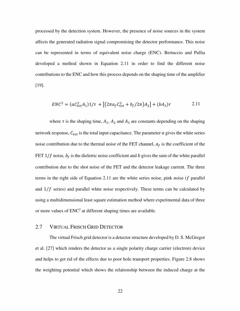
processed by the detection system. However, the presence of noise sources in the system
affects the generated radiation signal compromising the detector performance. This noise
can be represented in terms of equivalent noise charge (ENC). Bertuccio and Pullia
developed a method shown in Equation 2.11 in order to find the different noise
contributions to the ENC and how this process depends on the shaping time of the amplifier
[19].
�2( = (V2=?=( &W)1/X + Z)2[VS2=?=( + \S/2[-&(] + (\&^)X 2.11
where X is the shaping time, &W, &( and &^ are constants depending on the shaping
network response, 2=?= is the total input capacitance. The parameter V gives the white series
noise contribution due to the thermal noise of the FET channel, VS is the coefficient of the
FET 1/� noise, \S is the dieletric noise coefficient and \ gives the sum of the white parallel
contribution due to the shot noise of the FET and the detector leakage current. The three
terms in the right side of Equation 2.11 are the white series noise, pink noise (� parallel
and 1 �⁄ series) and parallel white noise respectively. These terms can be calculated by
using a multidimensional least square estimation method where experimental data of three
or more values of ENC2 at different shaping times are available.
2.7 VIRTUAL FRISCH GRID DETECTOR
The virtual Frisch grid detector is a detector structure developed by D. S. McGregor
et al. [27] which renders the detector as a single polarity charge carrier (electron) device
and helps to get rid of the effects due to poor hole transport properties. Figure 2.8 shows
the weighting potential which shows the relationship between the induced charge at the

23
anode and the depth of interaction. It can be observed that any charge moving from the
cathode to the anode does not induce any charge on the anode until it reaches the near grid
region. So the charged induced on the anode is free from any movement due to the holes
(as long as the interaction is not in the near grid region) and is solely due to movement of
electrons in the near grid region.
Figure 2.8. Variation of weighting potential as a function of interaction depth in a virtual
Frisch grid detector.
2.8 BIPARAMETRIC CORRELATION
Given a random distribution of hole trapping center within the detector thickness
and the fact that gamma rays of a particular energy can interact anywhere within the
detector thickness, signals with various rise-times and pulse-heights can be obtained for
that particular energy. For the interactions close to the cathode, the electron movements
form the major part of the signal, but for interactions close to the anode, hole movement
contributes more to the signal. Due to their poor transport properties, the holes drift slowly
compared to the electrons and hence the resulting signal has a higher rise-time. Finite
shaping times in spectroscopic amplifiers may not be sufficient to integrate the entire

24
charge pulse and obtain the full information i.e., the total charge, leading to an effect called
ballistic deficit. Moreover, the holes trapped in defect sites may eventually recombine
resulting in a partial charge induction on the anode. Thus, the events for gamma rays with
a particular energy may exhibit less pulse-height for interactions close to the cathode. The
ballistic deficit and the charge loss cause partial and randomly varying charge collection.
This effect is reflected as lower energy event leading to tailing of the full-energy peak at
the lower energy side.
The effect of charge loss to pulse-height spectra can be very easily visualized using
a biparametric plot. This analysis also allows to study the correlations between pulse height
and interaction depth for each gamma event [28]. The process to obtain a biparametric
analysis includes digital data acquisition, data processing, and correction. The data
acquisition process involves recording digitized pulses from the pre-amplifier. The
digitized pulses are shaped using a semi-Gaussian algorithm to filter out the noise required
for pulse-height determination. The rise-time was calculated as the time taken for the pre-
amplifier pulse height to rise from 10% to 90% of its maximum amplitude. The next step
involves generating a frequency table which shows the number of event with a particular
set of pulse-height and rise-time. A contour plot (biparametric plot) is generated based on
the frequency table which basically shows the frequency distribution of the rise-times and
pulse-heights.

25
Figure 2.9. Biparametric plot obtained for a CZT detector using a 137Cs source.
Figure 2.9 shows a biparametric plot obtained from a CZT detector using a 137Cs
source emitting 662 keV gamma rays. The inclination in the group of events corresponding
to the 662 keV interactions as seen in the figure is due to the two effects described
previously, ballistic deficit and charge loss. In an ideal case i.e., in the absence of charge
trap or loss, these events should appear as a vertically straight band of events. The deviation
from the ideal case can be corrected by implementing proper correction schemes which
recover the affected events to an improved situation close to the ideal case.
Figure 2.10 shows the biparametric plot shown in Figure 2.11 after the correction
applied to the pertinent group of events. In this case, it can be observed that the spectra
have been shifted to a position close to the ideal case. The correction scheme was developed
based on calculating the distances from the points of interest to a reference which is a line
parallel to the rise time axis and corresponding to the position of the unaffected events on
the pulse-height axis. Once the distances were calculated, the affected points are shifted to
the reference position. The correction scheme only changes the pulse-height (horizontal

26
change) of the events keeping the rise-time same because any change in the rise-time
indicates a different interaction depth which includes inconsistencies between the original
and corrected results. As a final step, a pulse height spectrum is regenerated from the
corrected pulse-heights in the biparametric plot as will be described in section 5.4.
Figure 2.10. Biparametric plot obtained after the application of a correction scheme to the
non-ideal biparametric plot shown in Figure 2.9.
27
CHAPTER 3: EXPERIMENTAL PROCEDURES
3.1 INTRODUCTION
This chapter describes the fabrication and characterization of 4H-SiC and CZT
radiation detectors. The fabrication process involves a series of steps depending on the
material properties and the type of incident radiation. The performance of a detector greatly
depends on the fabrication steps which involve ingot cutting, wafer dicing, cleaning,
surface polishing, surface passivation, and metal contact deposition. After the fabrication,
the detectors were characterized using current-voltage (I-V) and capacitance-voltage (C-
V) measurements. For spectroscopic characterization, pulse-height spectroscopy was
carried out using alpha and gamma radiation sources. A digital data acquisition system was
set up for implementing a biparametric correction. This chapter also describes the
development of various software codes necessary for data acquisition and processing used
in this work.
3.2 4H-SIC DETECTOR FABRICATION
The detectors are based on 20 µm thick n-type epitaxial layer, grown on a 4H-SiC
(0001) substrate highly doped with nitrogen and 4° off-cut towards the [112_0] direction.
Nomarski optical microscopy and scanning electron microscopy revealed a micropipe
defect density less than 1 cm-2. A 76 mm diameter parent wafer was diced in samples of
8x8 mm2 as is shown in Figure 3.1.

28
Figure 3.1. Photograph of an n-type 4H-SiC epitaxial layer wafer.
Before contact deposition, RCA standard wafer cleaning procedure was applied.
This process starts with the removal of organic contaminants (dust particles, grease, etc.)
from the wafer surface by using solvents (trichloroethylene, acetone, and methanol) at a
temperature of 70 °C. Any organic residue left by the first step is then processed using
sulfuric acid and ammonium hydroxide solutions (with hydrogen peroxide). These
solutions are designed to attack the organic impurities by dehydration process and
oxidation of the carbon present at the surface of the wafer. Finally, these oxide layers were
etched with hydrofluoric acid (HF). Figure 3.2 shows the schematic of the SiC wafer
consisting of the 4H-SiC epilayer, 4H-SiC buffer epilayer, and 4H-SiC bulk substrate.

29
Figure 3.2. Schematic diagram of n-type 4H-SiC epilayer wafer.
Nickel was deposited on the epilayer surfaces to form the Schottky barrier. This
deposition was achieved by using a Quorum Q150T DC sputtering unit. The deposited
Schottky contact thickness was ~10 nm with an area of ~11 mm2 (circular shape). Ohmic
back contact was achieved by depositing nickel (~100 nm thickness) with an area
approximately 6 x 6 mm2. Figure 3.3 shows a n-type 4H-SiC wafer with Ni deposited on
the epilayer face.
Figure 3.3. (a) Photograph of an actual 4H-SiC epitaxial Schottky barrier detector with nickel contact. (b) A detector mounted on a PCB.

30
The detectors were then mounted on printed circuit boards (PCB) and wire-bonded
for proper electrical connection. The wire-bonding was done using very thin (25 µm) gold
wire to ensure less scattering and obscuration of the alpha particles from the wire-bond
region. The PCBs were fitted with board-to-board connector pins in order to obtain plug-
in modular configuration for stable electrical connections as shown in Figure 3.3 (b).
3.3 CDZNTE DETECTOR FABRICATION
Several CZT ingots were grown in our laboratory using a Te solvent method [29]
and zone refined precursors [30]. CZT crystals of appropriate sizes have been cut out from
the ingot and lapped (down to 1µm SiC paper) and polished (down to 0.05 µm alumina
powder). The mechanically polished crystals were etched using a 1.5% Br2/methanol
solution for 60 seconds. In order to reduce the surface leakage currents, passivation of the
surface was performed by placing the detector in a Na2S solution for 15 minutes at a
temperature of 60 °C with argon bubbling to prevent oxidation.
Planar and virtual Frisch Grid detection configurations were applied for the
detectors fabrication process. First, approximately 70 Å thick gold contacts were deposited
on the two opposite surfaces (parallel to (111) crystallographic planes) for electrical
contacts using a Quorum Q150T sputtering unit. After the contact deposition step, the
planar configuration is completed. However, virtual Frisch grid configuration was achieved
with a copper sheath tightly wrapped around the crystal. The length of the copper sheath
covered the whole detector thickness. The sheath was electrically insulated from the CZT
material by lining the crystal side surfaces with insulating Teflon tape. The insulation
reduces the surface leakage current and prohibits leakage current from the sheath. The
copper sheath contained a projected tab which was used to connect it to the cathode as the

31
normal functional configuration of virtual Frisch grid detector needs the cathode and the
collar to be equipotential. Finally, these CZT detectors were mounted on PCBs and wire-
bonded as described for 4H-SiC detectors (see section 3.2).
3.4 ELECTRICAL CHARACTERIZATION
Current-voltage (I-V) and capacitance-voltage (C-V) measurements were
conducted, in order to investigate the electrical properties of the metal-semiconductor
contact. The I-V measurements were carried out using a Keithley 237 sourcemeter.
Forward and reverse bias characteristics were acquired to obtain the behavior of the
Schottky contact. C-V measurements were carried out at 100 kHz using a Keithley 590 C-
V meter. Figure 3.4 shows the schematic and the arrangement of the system in order to
perform the I-V and C-V measurements with the corresponding equipments.
Figure 3.4. Schematic of the experimental set-up for the I-V and C-V measurements.
3.5 ANALOG RADIATION DETECTION SYSTEM
Pulse-height spectra of alpha particles were recorded using an analog spectrometer
comprised of an Amptek CoolFet (A250CF) preamplifier, an Ortec 572 spectroscopy

32
amplifier, and a Canberra Multiport II ADC-MCA unit controlled by Genie 2000 interface
software. The radiation sources used were 0.1 µCi 241Am alpha source (5.48 MeV) with an
active diameter of 7mm and a 0.5µCi 137Cs (667 keV) gamma ray source. The source and
the detectors under test were placed inside an RFI/EMI shielded aluminum box.
For alpha particle measurements, the box was constantly evacuated (~10-3 mbar)
using a rotary pump in order to minimize the scattering of alpha particle with air molecules.
The radiation source was placed either illuminating the bottom or the top surface of the
detector depending on the specific requirements. Figure 3.5 shows a photograph of the 4H-
SiC epitaxial Schottky barrier detector inside RFI/EMI shielded test box.
Figure 3.5. Photograph of the 4H-SiC epitaxial Schottky barrier detector inside RFI/EMI
shielded test box.
After placing the detectors and the sources in a proper configuration in the test box,
the connections between the detector box, the pre-amplifier (A250CF), the NIM modules,
the oscilloscope, and the computer were made as shown in Figure 3.6.

33
Figure 3.6. Connection schematic for analog data acquisition set-up.
The charges generated in the detector due to the incident radiation energy are
collected by the A250CF, which is a charge sensitive low noise pre-amplifier and is best
suited for room-temperature detector operation. It hosts a Peltier cooled FET which helps
reducing the noise to a great extent. The voltage output of the pre-amp is then fed to an
amplifier (Ortec 671) which produces a shaped (semi-Gaussian) amplified output with
enhanced signal-to-noise ratio. This is achieved by using a band pass filter consisting of
differentiator and integrator circuits. The amplifier allows the user to select the shaping
time constant for optimized (trade-off between minimum noise and complete charge
collection time) detector performance. This amplified voltage output is directly
proportional to the incident energy of the radiation. The amplified output pulse is then fed
to a multichannel analyzer (MCA), which basically digitizes the amplifier output pulse
signal, and bins the pulses of similar heights in similar bins or channels to obtain a
histogram of the distribution of pulse height. The higher is the energy, higher is the channel
number. The resulting distribution is called a pulse-height spectrum or simply energy
spectrum. The MCA can be calibrated in various ways allowing the user to define each

34
channel in terms of energy. The software Genie 2000 was used to acquire and save pulse
height spectra and also to analyze the acquired data.
Figure 3.7. Schematic of the electrical connections for energy calibration.
Once the data is acquired, calibration process is performed in order to find a
correlation between the channels of the MCA with their corresponding energy. Figure 3.7
shows the connection schematic for energy calibration. It is important to note that the
calibration process should be done using the same settings as used in the actual experiment.
Epulser in keV was obtained by using Equation 3.1 where ε is the electron-hole pair creation
energy (7.7 eV for 4H-SiC and 4.64 eV for CZT [17]).
BT`�5@ = �BT`�5@ × � × 21.6 × 10*Wd 3.1
This calibration was accomplished by the injecting pulses of various known
amplitudes, Vpulser (mV), from a precision pulser (Ortec 419) through a calibrated feed-
through capacitor, to the preamplifier input and simultaneously noting down the peak-
positions of the shaped pulses in the multi-channel analyzer (MCA). A linear plot of the

35
peak centroid channel number against the keV equivalent pulser energy gives the required
calibration parameters [31].
3.6 DIGITAL RADIATION DETECTION SYSTEM
Digital data acquisition process was performed for gamma ray radiation detection.
In digital data acquisition system, the pre-amplifier pulses generated due to the incident
radiation are digitized using a digitizer and stored in a PC for online and offline processing.
Figure 3.8 shows the electrical connection arrangement for the digital data acquisition. A
NI PCI-5122 digitizer card was used to acquire pulses with a sampling rate of 100
Megasamples per second in real time and with a 14 bit vertical resolution.
Figure 3.8. Schematics of the electrical connection for digital data acquisition set-up.
A Labview based data-acquisition software was developed to acquire and store the
digitized pulses. The data analyses were performed using another program based on
Labview and Matlab. These analyses involved digital semi-Gaussian (CR-RC4) [32]
shaping of the pulses followed by pulse-height determination. Biparametric correlation was
carried out by mapping the pulse-height of the signal generated from a particular event and
the corresponding depth of interaction of that particular event in a 2D graph. The depth of
interaction was assumed to be proportional to the rise-time of the pulse. Deviation of the

36
correlation plots from the ideal behavior can be noticed when there are substantial charge-
loss effects associated with the gamma interaction events. Such deviations can be corrected
for by incorporating proper correction factors which restores the biparametric plots to a
near-ideal situation. Corrected pulse-height spectra were regenerated from the corrected
biparametric plots.

37
CHAPTER 4: 4H-SiC N-TYPE EPITAXIAL LAYER DETECTOR
4.1 INTRODUCTION
This chapter presents the results obtained from the electrical and spectroscopic
characterization of the 4H-SiC detectors. Surface barrier detectors were fabricated on 20
µm n-type 4H-SiC epilayers following the procedure described in Chapter 3 section 3.2.
The electrical characterization included current-voltage (I-V) and capacitance-voltage (C-
V) measurements that helped to determine the Schottky diode behavior e.g. leakage
current, barrier-height, ideality factor, and built-in potential. The C-V measurements also
helped to determine the effective doping concentration in the epilayer and the variation of
the depletion region area with the reverse bias. Alpha spectroscopic characterization was
performed to obtain pulse-height spectra to determine the energy resolution of the
fabricated detectors. The energy resolution is a conclusive parameter in order to determine
the performance of a detector. This chapter also describes the schemes developed to
determine the charge transport properties of minority carriers and to study the various
electronic components which define the ultimate detector performance.
4.2 ELECTRICAL CHARACTERIZATION
In order to identify the electrical properties of the detectors, I-V and C-V
measurements were conducted. I-V characteristics of the detectors at forward and reverse
bias were recorded at room temperature. The forward response is used to study the behavior

38
of the Schottky contacts using the thermionic emission model mentioned in section 2.2 in
terms of barrier height and the diode ideality factor. The value of barrier height obtained
from forward I–V characteristics is dominated by low Schottky barrier height locations in
an inhomogeneous Schottky diode [33]. The reverse I-V characteristics give the magnitude
of the leakage current under the operating conditions.
Figure 4.1. Room-temperature I-V characteristics at (a) forward and (b) reverse bias for Schottky barrier detector (S302).
Figure 4.1 shows the results of the I-V measurements for an n-type 4H-SiC
Schottky barrier detector S302. The forward response shows a near ideal diode behavior
with ideality factor 1.08 and a high surface barrier height of 1.6 eV. A diode ideality factor
so close to unity ensures barrier height uniformity across [22] the detector surface and such
a high barrier height ensures low leakage current. The reverse bias response accordingly
shows low leakage current of 1.84 pA at an operating reverse bias of - 90 V.
Table 4.1. I-V characteristics parameters for good quality Schottky contact.
Diode Name Current at -90V Barrier Height
(eV) Ideality Factor
S302 1.84 pA 1.613 1.08

39
Table 4.1 shows the calculated parameters from the forward and reverse bias
response of the detector S302. Such a low leakage current ensures a low parallel noise
required for high-resolution detector performance.
Figure 4.2. 1/C2 vs. V plot for n-type 20 µm epitaxial layer 4H-SiC detector. The solid line shows the linear fit to the experimental data. The original C-V plot has been shown
in the inset.
Figure 4.2 shows a 1/C2 vs V plot and the inset shows the original C-V plot. In a
Schottky metal-semiconductor junction, the depletion region extends to the side of the
semiconductor and increases its width with the increase in reverse bias. This property
allows to control the depletion width in epitaxial layer which defines the active region, the
region where the detection of the radiation takes place (creation of electron-hole pairs) of
the detector. As the capacitance value depends on the contact area and width of the
depletion region, as shown in section 2.3, it is expected to see a decrease in the capacitance
value when the reverse bias increases. Further analysis of the acquired data was performed
in order to calculate the doping concentration of the epilayer and the built-in voltage of the
Schottky contact. As expected, the capacitance values showed a decreasing trend with the
increasing reverse bias because of the increase in depletion width. An effective doping

40
concentration (Neff) of 2.4 × 1014 cm-3 was calculated from the slope of the linear fit of the
of 1/C2 vs V plot where A is the area, e is the electronic charge, �� is the permittivity of
vacuum and ��4e is the dielectric constant of 4H-SiC. Using the calculated value of doping
concentration in Equation 4.1, it is possible to calculate the voltage needed in order to fully
deplete the detector (thickness of the epilayer). The operating bias needed for full depletion
was calculated to be - 90 V for detector S302. It will be shown in the next section that the
optimum detector performance was obtained at a bias close to the full depletion width.
� = (�( × � × �5SS)2 × � × �� 4.1
where e is the electronic charge, �� is the permittivity of vacuum, � is the dielectric
constant of 4H-SiC and � is the width of the depletion region.
4.3 ALPHA SPECTROSCOPY MEASUREMENTS
The information obtained by the electrical characterization of the fabricated
detectors is useful in order to decide which detectors are suitable for spectroscopic
characterization. As discussed in the previous section, the detector S302 is a suitable
candidate for radiation detection. Spectroscopic characterization was performed using this
detector and a 0.1 µCi 241Am (5.48 MeV) alpha source. The spectrometer was set up
following the description in section 3.5.
Figure 4.3 shows the variation of charge collection efficiency (CCEobs) for alpha
particles calculated from detector S302 as a function of reverse bias. The CCEobs was
calculated as the ratio of the output energy observed by the detector to the actual incident
energy of the alpha particles (5.48 MeV). The contribution of the drift (CCEdepletion) and
diffusion (CCEdifussion) related charge collection to the observed total charge collection

41
efficiency was calculated using the drift-diffusion model [34] described in section 2.4.1
which was implemented using a Matlab based program.
Figure 4.3. Variation of CCEobs and CCEtheory as a function of reverse bias voltage. The contributions to the total CCE from charge drifts in depletion region (CCEdepletion) and
from hole diffusion in neutral region (CCEdifussion) are shown along with the variation of depletion width bias is also shown.
As it can be seen in Figure 4.3, at lower bias voltages, the contribution to the total
CCE is mostly dominated by the CCEdifussion. At lower bias the depletion width was smaller
than the alpha penetration depth (~ 18 µm in SiC for 5.486 keV alpha particle), in which
case most of the charge carriers were generated in the neutral region and the holes diffuse
to the depletion region to get collected. At higher bias, the charge collection efficiency is
dominated by the drifting of charge carriers within the depletion width because it becomes
comparable or higher than the alpha particle penetration depth Therefore, at a reverse bias
beyond -70 V, the CCEdepletion values were almost equal to the CCEobs values. The average
diffusion length (Ld) was calculated to be ~13.2 µm using the drift-diffusion model and the
Matlab code as described in section 2.5. Such a high diffusion length implies the possibility
of charge collection even at zero applied bias allowing these detectors to be used without

42
any applied bias [35]. It can be noticed from Figure 4.3 that at 0V applied bias, the CCEobs
is ~40% which indicates how effectively the detector can work by obtaining a robust alpha
peak at zero applied bias.
Figure 4.4. Variation of detector resolution as a function of reverse bias. The variation of
the pulser peak width is also shown.
Figure 4.4 shows the variation of detector energy resolution (FWHM) in keV and
percentage units as a function of reverse bias. The percentage resolution is the ratio
between the full-width half-maxima (FWHM) of the peak to the peak centroid. It can be
observed that the increment in the bias helped to improve the performance of the detector
due to the increased CCE at higher bias. At biases beyond - 70 V, the performance of the
detector gets almost saturated, however, experimental results indicated that the best
resolution was obtained at - 90 V. Figure 4.4 also shows the variation of the pulser peak
width (FWHM) as a function of bias. A systematic initial decrease of FWHM with
increasing bias was noticed which indicates the reduction in white series noise and pink

43
noise as the detector capacitance decreases with increase in reverse bias. The dependence
of electronic noise with capacitance is discussed in details in section 4.4.
Figure 4.5. Pulse height spectrum obtained using an n-type 4H-SiC epitaxial Schottky
detector (S 302) and an 241Am source. A pulser spectrum acquired simultaneously is also shown.
Figure 4.5 shows a pulse-height spectrum acquired using a 241Am source at an
optimized operating bias of -90 V and an amplifier shaping time of 3µs. The optimization
of the shaping time was carried out by studying the variation of the detector resolution with
the amplifier shaping time and will be described in the next section. The pulse-height
spectrum in Figure 4.5 shows three clearly resolved alpha peaks. These three peaks
correspond to the three major alpha emissions from the 241Am source and their theoretical
energies are 5388 keV, 5443 keV, and 5486 keV. The high resolution of the detector
allowed to clearly resolving these three peaks with a percentage resolution of 0.37% for
the 5486 keV peak. The width of the pulser peak recorded along-with was 7.3 ± 0.2 keV
which was less compared to the width observed for the 5486 keV peak (16.2 ± 0.2 keV)
implying that the detector performance was not limited by the pre-amplifier noise. The
peak width without the broadening due to the electronic noise is defined as the intrinsic
5000 5250 5500 5750 6000 6250 6500 6750 70000
50
100
150
200
250
300
FWHM= 14.9 keV
Co
un
ts
Energy (keV)
Data
Fitted Peaks
α1:
54
86
ke
Vα
2:
54
43
ke
V
α3:
53
88
ke
V
Pulser
FWHM= 20.73 keV

44
detector resolution which was calculated to be 14.5 keV following a quadrature sum rule
[24].
4.4 EQUIVALENT NOISE CHARGE ANALYSIS
As mentioned in the previous section, it is very important to determine the
electronic noise and its components as the ultimate detector resolution depends on them.
The equivalent noise charge (ENC) is the representation of the contribution of different
noise sources that influence in the radiation detection signal acquisition and processing.
These noise components were calculated using the formalism developed by Bertuccio and
Pullia [19] and has been described in section 2.4.1.
For the ENC measurements, the experimental set up was the same as used for
calibration procedure described in section 3.5. The electronic noise was measured from the
pulser peak width and expressed in terms of equivalent noise charge (ENC) in charge units
as described in section 2.4.1. Pulse-height spectra were acquired using the precission pulser
generating pulses at a fixed amplitude and frequency. The pulse-height spectra were
recorded as a function of amplifier shaping time. The ENC is plotted as a function of
amplifier shaping time τ and fitted to Equation 2.11 using a least square estimation method
implemented with Matlab coding as described in section 2.4.1. This program was designed
to apply the corresponding fitting to the experimental results in order to calculate the three
terms in the right side of Equation 2.11 which are the white series noise, pink noise (�
parallel and 1 �⁄ series) and parallel white noise respectively.

45
Figure 4.6. Variation of equivalent noise charge as a function of shaping time. The separate contributions from white series noise, white parallel noise, and pink noise are
also shown.
Figure 4.6 shows the variation of ENC and various noise contributions calculated
as a function of different shaping times. Figure 4.7 shows the same analysis, however, in
this particular case, a detector (biased and exposed to the alpha source) is connected to the
pre-amplifier. By comparing both the figures, it is possible to see that the ENC is higher
when the detector is connected to the system. At any given shaping time, it can be seen
from Figure 4.8 that the magnitude of the white parallel noise increased by a factor of ~5
and the white series noise increased by an order of magnitude. The pink noise, which is
independent from the shaping time, increased marginally from 156 to 207 Coulomb rms.
The white parallel noise increment is due to the additional current from the detector while
the increase in white series noise was due to the increase in the input capacitance (detector
capacitance was ~55.2 pF at - 90 V). Also, the minimum ENC achievable was different
shaping times for the two cases. For Figure 4.6, it can be seen that the minimum ENC was
obtained at a shaping time between 1 and 2 µs when the detector was not connected to the
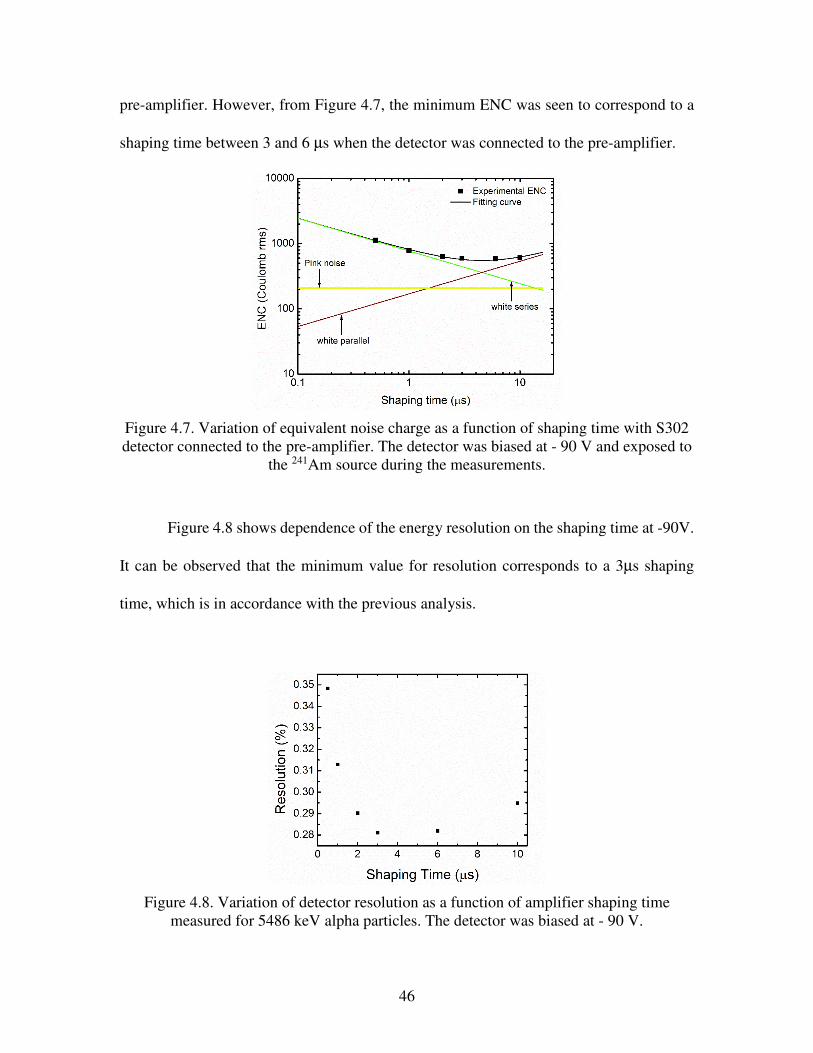
46
pre-amplifier. However, from Figure 4.7, the minimum ENC was seen to correspond to a
shaping time between 3 and 6 µs when the detector was connected to the pre-amplifier.
Figure 4.7. Variation of equivalent noise charge as a function of shaping time with S302 detector connected to the pre-amplifier. The detector was biased at - 90 V and exposed to
the 241Am source during the measurements.
Figure 4.8 shows dependence of the energy resolution on the shaping time at -90V.
It can be observed that the minimum value for resolution corresponds to a 3µs shaping
time, which is in accordance with the previous analysis.
Figure 4.8. Variation of detector resolution as a function of amplifier shaping time
measured for 5486 keV alpha particles. The detector was biased at - 90 V.

47
Figure 4.9. Variation of ENC, white series noise and white parallel noise, measured using
3 µs shaping time, as a function of different bias voltages/detector capacitances.
Figure 4.9 shows the variation of ENC and the separate noise contributions to the
overall ENC as a function of applied reverse bias and at an optimized shaping time of 3 µs.
The detector junction capacitance reduces and the leakage current increases with the
applied reverse bias. Also, the contribution of white series noise dominated towards the
overall noise and decreases with the increasing reverse bias (or decreasing capacitance).
The white parallel noise, that also includes the detector leakage current, was seen to
contribute the least at lower biases and increase with reverse bias due to the increase in
leakage current. Finally, it can be observed that beyond -50 V bias, the white parallel noise
contribution exceeds that of the pink noise.
4.5 CONCLUSION
Electrical and spectroscopic characterizations were performed on 4H-SiC detectors
fabricated on 20 µm n-type 4H-SiC epilayers. I-V characteristics revealed the Schottky
behavior of the detector (S302). Using a thermionic emission model, the barrier height and
diode ideality factor were calculated to be 1.6 eV and 1.08 respectively. The leakage

48
current at - 90 V was 1.84 pA. Analysis of the C-V measurements revealed a doping
concentration of (Neff) of 2.4 × 1014 cm-3 and allowed to calculate the bias needed to full
depletion of the epilayer which is - 90 V. The electrical characterization results indicated
that S302 is suitable for radiation detection. Spectroscopic characterization was performed
on S302 detector with 241Am alpha source. A Matlab code was developed to employ a drift-
diffusion model which fits the variation of CCE with reverse bias. A diffusion length of
~13.2 µm was calculated using the drift-diffusion model. The percentage energy resolution
for 5486 keV peak was found to be 0.37% at - 90V and 3µs of shaping time. Electronic
noise in terms of equivalent noise charge (ENC) as a function of shaping time was
analyzed. A Matlab code was developed in order to calculate the contribution of each type
of noise to the total ENC. The contribution of the white series noise to the overall ENC
was found to dominate compared to the white parallel and the pink noise up to a reverse
bias of -120 V and decrease steadily with decreasing capacitance. The contribution of pink
noise was seen to be more than that of the white parallel noise for bias voltages less than -
50 V and beyond which the contribution of white parallel noise became more because of
the increased leakage current.

49
CHAPTER 5: GAMMA SPECTROSCOPY USING CZT DETECTOR AND APPLICATION OF BIPARAMETRIC
CORRECTION SCHEME
5.1 INTRODUCTION
Cd0.9Zn0.1Te (CZT) is an excellent material for gamma ray detection and
spectroscopy because of its high average atomic number, high density, and high band gap.
However, CZT crystals suffer from poor charge transport properties, especially for holes.
The adverse effect of poor hole transport properties can be compensated for adopting
offline digital correction schemes to digitally acquired radiation interaction data. One such
scheme is biparametric correction.
This chapter presents the results obtained from the characterization of CZT gamma
radiation detectors. Three detectors were used for the present study: two with virtual Frisch
grid (detector D1 and D2) and one in planar detector geometry (detector A) shown in Figure
5.1. Current-voltage (I-V) measurements were conducted to calculate the resistivity of the
materials and to observe the magnitude of the leakage current. For spectroscopic
characterization a 0.5 µCi 137Cs (662 keV) gamma source was used to obtain gamma pulse-
height spectrum. A digital spectrometer was set up to acquire digitized pulses from the
detectors. Pulse-height spectra were obtained from the three detectors using an analog and
the digital spectrometer. A software code based on Matlab and Labview was developed to
implement a biparametric correction scheme to the digitally obtained pulses. A study of

50
difference of biparametric plots and associated correction scheme between planar and
Frisch grid configuration has also been presented.
Figure 5.1. Photograph of the three CZT used in the present study. Detectors (a) Planar detector A and (b) Virtual Frisch grid detectors D1 and D2.
5.2 ELECTRICAL CHARACTERIZATION
As it was described in section 3.3, CZT detectors were fabricated with by depositing
gold contacts on the two opposite surfaces of CZT single crystals. I-V characteristics were
obtained for negative and positive bias in order to verify the contact behavior of the
detectors. Resistance of the detectors was calculated from the slope of the linear section of
the I-V plot, which is used in Equation 5.1 to calculate the resistivity of the CZT detectors.
f = g × &N 5.1
where g is the resistance of the detector, & is the active contact area and N is the
thickness of the detector. Low leakage current and high resistivities are the indicative of
good radiation detection.
Figure 5.2(a) shows the I-V characteristics obtained from the planar detector A. It
can be observed that there is a distinct asymmetry in the current behavior in the negative
and positive bias regime indicating the presence of active deep center at the surfaces which
can render the Au/CZT interface as non-Ohmic depending on whether the surface is Cd or

51
Te rich [36]. The reverse bias response of the detector revealed a current of ~10 nA at -
1000 V, while the forward response showed a current of ~1 µA at 500 V. Figure 5.2 (b)
shows a low range I-V measurements for resistivity determination. Using Equation 5.1, the
bulk resistivity of detector A was calculated to be 6.7 × 10¹⁰ Ω-cm.
Figure 5.2. (a) I-V curve obtained for CZT crystal A with planar gold contacts. (b) Linear region of the I-V curve for resistivity measurements.
Figure 5.3. Room temperature current-voltage characteristics of detectors D1 and D2 in
virtual Frisch grid geometry.

52
Figure 5.3 shows the results of the I-V measurements for detectors D1 and D2 in
virtual Frisch grid geometry. It can be observed that the I-V characteristics were nearly
symmetric in the positive and the negative bias ranges, confirming the Ohmic nature of the
gold contacts. The response for positive bias revealed a current of ~11 nA for detector D1,
and ~8 nA for detector D2 at 1000 V. The magnitude of leakage currents in detector D2
was found to be smaller compared to that in the detector D1 because of its smaller area and
larger thickness. Using Equation 5.1, the bulk resistivity obtained for detectors D1 and D2
are 3.42 × 10¹⁰ Ω-cm and 1.99 × 10¹⁰ Ω-cm respectively. For room temperature nuclear
detection application, the desired leakage current in a CZT crystal is achievable when its
resistivity is close to ~1010 Ω-cm [37] [38]. Therefore, the resistivity values obtained for
the present detectors indicate that they are suitable for room temperature radiation
detection.
5.3 GAMMA SPECTROSCOPY
Spectroscopic characterization was performed using a 0.5 µCi 137Cs (662 keV) and
a 0.1 µCi 241Am (59.5 keV) gamma sources. The measurements were conducted following
the description in section 3.6.
Figure 5.4 shows the pulse-height spectrum acquired using a 241Am gamma source
and planar detector A biased at 700 V. In a planar detector, the weighting potential or
induced charge depends on the depth of radiation interaction. This may render the
performance of the detector inefficient because the gamma rays can interact at any arbitrary
depth within the detector (particularly for high energy gamma rays). The signal due to the
interactions at a considerable depth will be generated by the movement of both electrons

53
and holes. Since CZT has poor hole transport properties, such signals can considerably
affect the detector performance.241Am emits low energy gamma rays (59.5 keV) which
indicates that the interactions are close to the signal collecting surface. Therefore, the
radiation signal produced is mainly due to the movement of electrons under a proper
selection of the polarity of the bias. The energy resolution for the planar detector A was
calculated for 59.5 keV gamma rays from the pulse-height spectrum shown in Figure 5.4
to be ~7.4%.
Figure 5.4. Gamma pulse-height spectra obtained using a 241Am source from planar
detector A.
Figure 5.5. Gamma pulse height spectra obtained using a 137Cs source from planar
detector A.

54
Figure 5.5 shows the pulse-height spectrum acquired using a 137Cs gamma ray
source from planar detector A at a bias of 900 V. Since 137Cs is a high energy (662 keV)
gamma ray source the interactions primarily occur deep within the detector. Therefore, the
detection signals are produced due to the movement of both holes and electrons. This is
evident from Figure 5.5 as the prominent spectral features like the full-energy peak, the
back scattered peak, etc. were absent in the pulse-height spectrum.
Figure 5.6 shows a 241Am (59.6 keV gamma rays) spectrum obtained using the
virtual Frisch grid detectors D1 and D2 biased at 550 V and 1500 V respectively. The
percentage energy resolution obtained for detector D1 was 6.1% and for detector D2 is
8.7%. Comparing the performance of planar detector B and Frisch grid detectors D1 and
D2, it is possible to observe that the configuration of the detector does not have
considerable influence on its performance for detecting low energy gamma rays as far as
the energy resolution is concerned.
Figure 5.6.241Am spectrum obtained using Frisch grid detector D1 (a) and detector D2 (b)
at 550 V and 1500 V bias respectively.

55
Figure 5.7. 137Cs pulse-height spectrum obtained using Frisch grid detector D1 (a) and
detector D2 (b) at 1200 V and 1500 V bias respectively.
Figure 5.7 shows the spectral response of the detector D1 and D2 exposed to 137Cs
gamma ray and biased at 1200 V and 1500 V respectively. The full energy peak
corresponding to the 662 keV gamma rays was clearly resolved for detector D1. Also, other
spectral features like the Compton edge and the backscattered peak were distinctly visible
for both detectors. The percentage energy resolution was found to be 1.6% for detector D1
and 5.9% for detector D2. The peak-to-valley ratio (P/V) was 2.6 for detector D1, however,
for detector, D2 the P/V value was less than 1. From the spectrum obtained from the
detector D2, it can be observed that the full energy peak exhibit much lower energy than
662 keV. Low peak-to-valley ratio and peak-energy mismatch indicate incomplete charge
collection due to insufficient strength of the applied electric field or bias. However,
increasing the applied bias did not result in improved performance as the leakage current
was seen to increase accordingly resulting in increase in parallel noise. It could not be
confirmed whether the poor resolution (or poor charge collection) observed for detector
D2 is due to the insufficient strength of the electric field or due to the trapping of charges
in defect centers.

56
5.4 BIPARAMETRIC PLOT AND CORRECTION SCHEME
The poor performance of the planar detector A and virtual Frisch grid detector D2
for high energy gamma rays can be recovered using a biparametric correction scheme. In
biparametric plots, the pulse-heights from the same energy events are correlated to their
corresponding depth of interaction. A biparametric plots is basically a three-dimensional
plot with the x-axis representing the pulse-heights, the y-axis representing the rise-time,
and the number of events displayed by graded color. Any anomalies in the correlation
between pulse-heights and depth of interaction can be identified from a biparametric plot.
As has been mentioned in section 2.5, a Matlab based program was developed in order to
generate the biparametric plot and to apply the correction scheme.
Figure 5.8. Biparametric plot obtained from interaction of 662 keV gamma rays with the
planar detector A: (a) uncorrected and (b) corrected.
Figure 5.8(a) shows a biparametric plot generated for the planar detector A
irradiated with a 137Cs source. The events within the yellow dotted lines shows the 662 keV
photoelectric events. If the detector had been free of charge traps, these events would have
appeared as a vertically straight band (parallel to the rise-time axis) of correlated events.
However, it can be clearly seen that there is an inclination of the band of the events which
in turn indicates that the variation of signal amplitude as a function of depth of interaction

57
for the 662 keV photoelectric events was affected by charge loss/trapping. In order to
recover the pulse-height spectrum from the effect of the hole-trapping, the developed
Matlab based correction scheme was applied to the region of interest (yellow lined area).
The results of the correction process are shown in Figure 5.8(b) where it can be observed
that the 662 keV events appear as vertically straight resembling a charge-trap free detector.
Figure 5.9. 137Cs pulse-height spectrum regenerated after an application of a correction scheme to the biparametric plot shown in Figure 5.8. The dotted lines show the digital pulse-height spectrum obtained before the biparametric correction. The inset shows the
magnified region of the 662 keV peak for the corrected and uncorrected spectra.
Figure 5.9 shows the corrected pulse-height spectrum regenerated from the
corrected biparametric plot (Figure 5.8). Spectral features like the photo-peak and the
Compton edge are clearly visible. A distinct 662 keV peak could be seen in the corrected
plot. The percentage energy resolution was calculated to be of 3.6 % for the 662 keV
gamma rays.
Figure 5.10 shows the biparametric plot obtained using a 137Cs source for detector
D1. The 662 keV full-energy events marked by the dotted lines can be clearly distinguished
from the Compton events in the biparametric plot. As has been described earlier, for virtual

58
Frisch grid detectors, the generated signals are primarily due to the movement of the
electrons and that too when they are very close the collection electrode. Hence the
generated signals are mostly free from charge trapping effects. It can be observed in the
case for detector D1, where the 662 keV events appear as a vertically straight band.
Figure 5.10. Biparametric plot obtained using a 137Cs source for Frisch grid detector D1
[39].
Figure 5.11. Biparametric plot obtained from interaction of 662 keV gamma rays with the
planar detector D2: (a) uncorrected and (b) corrected.
On the other hand, Figure 5.11(a) shows a biparametric plot generated for the Frisch
grid detector D2 irradiated with 137Cs source. The white dotted lines show the 662 keV
photoelectric events. These events were inclined toward the high energy side of the actual

59
peak position, which is the opposite case from the normal hole trapping effect in planar
detector A. This atypical behavior can still be attributed to the hole trapping and de-
trapping effect. Figure 5.12 shows two instances of positions of interactions marked as P1
and P2. In the case of interaction at P2, the induced signals would be due to the combined
electron-hole movement. The hole current will be affected by their trapping and de-
trapping in the detect sites resulting in longer pulse rise-times. On the other hand, for
interactions at P1, the output signal will be primarily due to the electron movements. So
the induced charge is expected to be less than that of combined charge induction from both
electrons and holes and hence shows a lower pulse-height. Since the electron movements
are comparatively faster, the rise-times will be smaller for these interactions. This explains
why the events with higher rise-time exhibit higher pulse-heights.
Figure 5.12. Weighting potential distribution in a Frisch grid detector as a function of depth of interaction.
Figure 5.11(b) shows the biparametric plot after applying the developed Matlab
based correction scheme to the plot shown in Figure 5.11(a). The positive slope inclined
events were selectively aligned to the 662 keV line. The corrected pulse-height spectrum
regenerated from the corrected biparametric plot is shown in Figure 5.13. It can be

60
observed that the photo-peak have a narrower distribution after the correction with a
percentage energy resolution of 3.13% for 662 keV gamma rays.
Figure 5.13. 137Cs pulse-height spectrum generated after an application of Matlab based
correction scheme to the biparametric plot shown in Figure 5.11(b).
5.5 CONCLUSION
Electrical and spectroscopic characterizations were performed on Cd0.9Zn0.1Te
detectors. Three detectors were fabricated: two with virtual Frisch grid (detector D1 and
D2) and one with planar detector (detector A) configuration. I-V measurements revealed
resistivity greater than 1010 Ω-cm. The typical magnitude of leakage current was found to
be of the order of few nA at operating voltages. The electrical characterization results
indicated that the detectors are suitable for radiation detection. Spectroscopic
characterization was performed using a 241Am (59.5 keV) and a 137Cs (662 keV) gamma
ray sources. From 241Am gamma pulse-height spectra, the percentage energy resolution of
the detectors was found to be 7.4% for detector A, 6.1% for detector D1 and 8.7% for
detector D2. From 137Cs gamma pulse-height spectra, the percentage energy resolution of
the detectors was calculated to be 1.6% for detector D1 and 5.9% for detector D2. There

61
was no discernable peak obtained for detector A for 662 keV gamma ray. Biparametric
plots were generated from digitally acquired data using the three detectors and the 137Cs
gamma ray source. Analyses of these plots revealed that detector A and detector D2 suffer
from excessive hole charge trap/loss. A biparametric correction scheme was developed in
Matlab to recover the pulse-height spectra. It was observed that the application of the
biparametric correction scheme improved the results acquired from the detectors by
recovering the pulse-height spectrum from the charge trapping effects.

62
CHAPTER 6: CONCLUSION AND FUTURE WORK
6.1 CONCLUSION
This thesis is focused on the fabrication and characterization of semiconductor
based radiation detectors for alpha particles and gamma rays and development of various
software codes (based on Matlab) required to derive important device parameters from the
experimental results in order to improve the device performance. Two kind of
semiconductor detectors have been chosen for this study viz., epilayer based n-type 4H-
SiC detectors for alpha detection and high resistive Cd0.9Zn0.1Te based x/γ-ray detection.
The characterization techniques employed to study the detectors are based on electrical
measurements which include current and capacitance studies and spectroscopic techniques
which involve alpha and gamma detection.
For alpha particle detection, Schottky devices were fabricated on high quality 4H-
SiC epitaxial layers. Current-voltage (I-V) and capacitance-voltage (C-V) were measured
to investigate the Schottky barrier properties. The I-V characteristics revealed extremely
low leakage current of the order of few pA at operating reverse biases close to 100 V. Large
Schottky barrier heights of the order of 1.6 eV (calculated by using a thermionic emission
model) helped to obtain such low leakage currents. Alpha spectroscopic measurements
performed using a 241Am radiation source revealed a percentage energy resolution of
~0.37% for 5486 keV peak. A Matlab based code was developed to fit the experimentally
obtained CCE vs bias data to a drift-diffusion model and to calculate the minority carrier
diffusion length (Ld). High values of the order of ~13.2µm were calculated for these diodes.

63
Electronic noise in terms of equivalent noise charge (ENC) as a function of shaping time
was analyzed. A Matlab code was developed based on the ENC formalism developed by
Bertuccio and Pullia [19] in order to calculate the contribution of each type of noise to the
total ENC. The ENC analyses results showed that the electronic noise increased when the
detector is plugged in to the pre-amplifier due to the added detector capacitance and leakage
current. The measurements also helped to understand that better energy resolution could
be obtained by reducing the junction capacitance i.e., by using thicker epilayers.
Gamma ray detectors were fabricated using Cd0.9Zn0.1Te (CZT) single crystal
grown in our laboratory using a Te solvent method. CZT is a high Z compound
semiconductor material with convenient properties for gamma ray detection. Three
detectors were fabricated: two with virtual Frisch grid (detector D1 and D2) and one with
planar detector (detector A) configuration. I-V measurements revealed resistivities greater
than 1010 Ω-cm. The typical magnitude of leakage current was found to be of the order of
few tens of nA at operating voltages close to 1000V. Spectroscopic characterizations were
performed using an 241Am (59.5 keV) and a 137Cs (662 keV) gamma ray sources. All the
detectors irrespective of their configuration showed highly resolved gamma spectra for
241Am low-energy gamma source. For high energy gamma rays (662 keV) both the virtual
Frisch grid detectors revealed the 662 keV peak, however the planar detector was found to
suffer from the charge loss effects. Biparametric plots were generated from digitally
acquired data using the three detectors and the 137Cs gamma ray source. Analyses of these
plots confirmed that detector A suffers from excessive hole charge trap/loss. A
biparametric correction scheme was developed in Matlab to recover the pulse-height
spectra. It was observed that the application of the biparametric correction scheme

64
improved substantially the results acquired from the detectors by recovering the pulse-
height spectrum from the charge trapping effects spectra.
6.2 FUTURE WORK
It has been proven that 4H-SiC epitaxial layer is an excellent material for
fabrication of alpha particle detectors due to its high band gap and excellent crystallinity.
In order to step forward in the improvement of the detector performance certain additional
techniques can be adopted during the detector fabrication process. Passivation of the
detector surfaces is one such approach to improve the detector performance by eliminating
the effect of the surface states that mediates surface current flow. This process also
improves the metal-semiconductor edge interface leading to high break down voltages.
Silicon dioxide (SiO2) and silicon nitride (Si3N4) are suitable materials for growing an
oxide or nitride layer on SiC which can act as passivating layers. SiO2 or S3N4 can be
deposited by plasma-enhanced chemical vapor deposition (PECVD).
It has been studied only two configurations for CZT gamma ray detectors, planar
geometry and virtual Frisch grid. However, other types of detector geometries can be
investigated such as co-planar, multiple small pixel, and guard-ring.

65
REFERENCES
[1] F. Nava, G. Bertuccio, A. Cavallini, and A. E. Vittone, "Silicon carbide and its use as a radiation detector material," Measurement Science and Technology, vol. 19, pp. 102001-102025, 2008.
[2] K. C. Mandal, P. G. Muzykov, S. K. Chaudhuri and J. R. Terry, "Low Energy X-Ray and γ-Ray Detectors Fabricated on n-Type 4H-SiC Epitaxial Layer," IEEE
Transactions on Nuclear Science, vol. 60, pp. 2888-2893, 2013. [3] F. Moscatelli, A. Scorzoni, A. Poggi, M. Bruzzi, S. Sciortino, S. Lagomarsino, G.
Wagner, I. Mandic, and R. Nipoti, "Radiation Hardness After Very High Neutron Irradiation of Minimum Ionizing Particle Detectors Based on 4H-SiC p+n Junctions," IEEE Transactions on Nuclear Science, vol. 53, no. 3, pp. 1557-1563, 2006.
[4] K. C. Mandal, R. M. Krishna, P. G. Muzykov, S. Das and T. S. Sudarshan, "Characterization of Semi-Insulating 4H Silicon Carbide for Radiation Detectors," IEEE Transactions on Nuclear Science, vol. 54, pp. 1992-1999, 2011.
[5] P. G. Muzykov, R. M. Krishna and K. C. Mandal, "Temperature dependence of current conduction in semi-insulating 4H-SiC epitaxial layer," Applied Physics
Letters, vol. 100, pp. 032101-032105, 2012. [6] S. Wang, M. Dudley, C. H. Carter Jr. and H. S. Kong, "X-Ray Topographic Studies
of Defects in PVT 6H-SiC Substrates and Epitaxial 6H-SiC Thin Films," Materials
Research Society, vol. 339, pp. 735-740, 1994. [7] Q. Wahab, A. Ellison, A. Henry, E. Janzén, C. Hallin, J. Di Persio and R. Martinez,
"Influence of Epitaxial Growth and Substrate Induced Defects on the Breakdown of High-voltage 4H-SiC Schottky Diodes," Materials Science Forum, vol. 338, pp. 1175-1178, 2000.
[8] R. V. Badcock and H. C. Chang, "SiC Neutron Detectors for High Temperature Operation, Neutron Dosimetry," Proceedings of the Symposium on Neutron
Detection, Dosimetry and Standardization, vol. 1, pp. 613-622, 1962. [9] H. Ruddy, A. R. Dulloo, J. G. Seidel, S. Seshari and L. B. Rowland, "Development
of a Silicon Carbide Radiation Detector," IEEE Transactinos on Nuclear Science,
vol. 45, pp. 536-541, 1998. [10] F. Nava, P. Vanni, C. Lanzieri and C. Canali, "Epitaxial silicon carbide charge
particle detectors," Nuclear Instruments and Methods in Phys. Research A, vol. 437, no. 2-3, pp. 354-358, 1999.
[11] F. Ruddy, A. Dulloo, J. Seidel, J. Palmour and R. Singh, "The charged particle response of silicon carbide semiconductor radiation detectors," Nuclear Instruments
and Methods in Physics Research A, vol. 505, pp. 159-162, 2003.

66
[12] F. H. Ruddy, J. G. Seidel, H. Chen, A. R. Dulloo and S.-H. Ryu, "High-Resolution Alpha-Particle Spectrometry Using 4H Silicon Carbide Semiconductor Detectors," IEEE Transactions on Nuclear Science, vol. 53, pp. 1713-1718, 2006.
[13] F. Ruddy, J. Seidel and P. Sellin, "High-resolution alpha spectrometry with a thin-window silicon carbide semiconductor detector," Proceedings of the IEEE Nuclear
Science Symposium Conference Record (NSS/MIC), pp. 2201-2206, 2009. [14] A. Pullia, G. Bertuccio, D. Maiocchi, S. Caccia and F. Zocca, "An SiC/GaN
Detector/Front-End Detection System for High-Resolution Alpha-Particle Spectroscopy," IEEE Transactions on Nuclear Science, vol. 55, pp. 3736-3740, 2008.
[15] B. Milbrath, A. Peurrung, M. Bliss and W. Weber, "Radiation detector materials: An overview," Journal of Materials Research, vol. 23, pp. 2561-2581, 2008.
[16] S. D. Sordo, L. Abbene, E. Caroli, A. M. Mancini, A. Zappetteni and P. Ubertini, "Progress in the Development of CdTe and CdZnTe Semiconductor Radiation Detectors for Astrophysical and Medical Applications," Sensors, vol. 9, pp. 3491-3526, 2009.
[17] A. Owens and A. Peacock, "Compound semiconductor radiation detectors," Nuclear Instruments and Methods in Physics Research A, vol. 531, pp. 18-37, 2004.
[18] T. E. Schlesinger and R. B. James, Eds., Semiconductors for Room Temperature Nuclear Detector Applications, San Diego: Academic Press Inc., 1995.
[19] G. Bertuccio and A. Pullia, "A method for the determination of the noise parameters in preamplifying systems for semiconductor radiation detectors," Reviews of Scientific Instruments , vol. 64, pp. 3294-3298, 1993.
[20] S. M. Sze and K. K. Ng, "Metal-Semiconductor Contacts," in Physics of
Semiconductor devices, Hoboken, New Jersey, John Wiley & Sons, Inc., 2007, pp. 134-190.
[21] E. H. Rhoderick and R. H. Williams, Metal-Semiconductor Contacts, Oxford: Clarendon Press, 1988.
[22] R. T. Tung, "Electron transport at metal-semiconductor interfaces: General theory," Physical Review B, vol. 45, pp. 13509-13523, 1992.
[23] B. G. Streetman and S. K. Banerjee, Solid State Electronic Devices, New Jersey: Pearson Education Inc. , 2009.
[24] G. F. Knoll, Radiation Detection and Measurement, 3rd ed., New York: John Wiley & Sons, Inc., 2000.
[25] M. B. H. Breese, "A theory of ion beam induced charge collection," Journal of
Applied Physics, vol. 74, pp. 3789-3799, 1993. [26] J. F. Ziegler, J. Biersack and U. Littmark, The Stopping and Range of Ions in
Matter, New York: Pergamon Press, 1985. [27] D. McGregor, R. Rojeski, Z. He, D. Wehe, M. Driver and M. Blakely,
"Geometrically weighted semiconductor Frisch grid radiation spectrometers," Nuclear Instruments and Methods in Physics Research A, vol. 422, pp. 164-168, 1999.

67
[28] S. K. Chaudhuri, A. Lohstroh, M. Nakhostin and P. J. Sellin, "Digital pulse height correction in HgI2 γ-ray detectors," Journal of Instrumentation, vol. 7, p. T04002, 2012.
[29] R. M. Krishna, S. K. Chaudhuri, K. J. Zavalla and K. C. Mandal, "Characterization of CdZnTe based virtual Frisch grid detectors for high energy gamma ray detection," Nuclear Instruments and Methods in Physics Research A, vol. 701, pp. 208-213, 2013.
[30] S. K. Chaudhuri, R. M. Krishna, K. J. Zavalla, L. Matei, V. Buliga, M. Groza, A. Burger and K. C. Mandal, "Cd0.9Zn0.1Te Crystal Growth and Fabrication of Large Volume Single-Polarity Charge Sensing Gamma Detectors," IEEE Transactions on
Nuclear Science, vol. 60, pp. 2853-2858, 2013. [31] S. K. Chaudhuri, K. J. Zavalla and K. C. Mandal, "Experimental determination of
electron-hole pair creation energy in 4H-SiC epitaxial layer: An absolute calibration approach," Applied Physics Letters, vol. 102, pp. 031109-1-4, 2013.
[32] M. Nakhostin, "Recursive Algorithms for Real-Time Digital CR-(RC)n Pulse Shaping," IEEE Transactions on Nuclear Science, vol. 58, pp. 2378-2381, 2011.
[33] S. K. Chaudhuri, R. M. Krishna, K. J. Zavalla and K. C. Mandal, "Schottky barrier detectors on 4H-SiC n-type epitaxial layer for alpha particles," Nuclear Instruments
and Methods in Physics Research A, vol. 701, pp. 214-220, 2013. [34] M. B. H. Breese, A. Saint, F. W. Sexton, K. M. Horn, H. Schone, B. L. Doyle, J. S.
Laird and G. J. F. Legge, "Optimization of ionbeam induced charge microscopy for the analysis of the integrated circuits," Journal of Applied Physics, vol. 77, pp. 3734-3741, 1995.
[35] S. K. Chaudhuri, K. J. Zavalla and K. C. Mandal, "High Resolution Alpha Particle Detection Using 4H-SiC Epitaxial Layers: Fabrication, Characterization, and Noise Analysis," Nuclear Instruments and Methods in Physics Research A, vol. 728, pp. 97-101, 2013.
[36] J. Crocco, H. Bensalah, Q. Zheng, V. Corregidor, E. Avles, A. Castaldini, B. Fraboni, D. Cavalcoli, A. Cavallini, O. Vela and E. Dieguez, "Study of asymmetries of Cd(Zn)Te devices investigated using photo-induced current transient spectroscopy, Rutherford backscattering, surface photo-voltage spectroscopy, and gamma ray spectroscopies," Journal of Applied Physics, vol. 112, pp. 074503-1-9, 2012.
[37] T. Schlesinger, J. Toney, H. Yoon, E. Lee, B. Brunett, L. Franks and R. James, "Cadmium zinc telluride and its use as a nuclear radiation detector material," Materials Science and Engineering, vol. 32, pp. 103-189, 2001.
[38] A. Burger, H. Chen, K. Chattopadhyay, D. Shi, S. Morgan, W. Collins and R. James, "Characterization of metal contacts on and surfaces of cadmium zinc telluride," Nuclear Instruments and Methods in Physics Research A, vol. 428, pp. 8-13, 1999.
[39] S. K. Chaudhuri, K. J. Zavalla, R. M. Krishna and K. C. Mandal, "Biparametric analyses of charge trapping in Cd0.9Zn0.1Te based virtual Frisch grid detectors," Journal of Applied Physics, vol. 113, pp. 074504-1-6, 2013.

68
APPENDIX A - CCE FITTING MATLAB CODE
[Bias CCE]=textread('BiasCCE.txt'); [dEdx x]=textread('dedx.txt'); Ep=5.48e3; Eo=8.854e-12; Er=9.72; q=1.6e-19; Nd=2.4e8; %Depletion Width W=sqrt((Eo*Er*2*Bias)/(q*Nd)); for i=1:size(W) less=100; for j=1:size(x) diff= W(i)-x(j); pos(1)=1; if((diff<less) && (diff>0)) less=diff; pos(i)=j; end end if(pos(i)>1) %CCE-Drift CCEdrift(i)=(1/Ep)*trapz(x(1:pos(i)),dEdx(1:pos(i))); end end aux=abs(CCE-CCEdrift'); for i=1:8 %CCE-Diffusion diff=10; Lp(i)=1; while(diff>0.001) CCEdiff(i)=(1/Ep)*trapz(x(pos(i)+1:100),(dEdx(pos(i)+1:100)).*exp(-1*(x(pos(i)+1:100)-W(i))./Lp(i))); diff=abs(CCEdiff(i)-aux(i)); test(i)=diff; Lp(i)=Lp(i)+0.01; end end for i=9:11 %CCE-Diffusion diff=10; Lp(i)=1; while(diff>0.001) CCEdiff(i)=(1/Ep)*trapz(x(pos(i)+1:100),(dEdx(pos(i)+1:100)).*exp(-1*(x(pos(i)+1:100)-W(14))./Lp(i)));

69
diff=abs(CCEdiff(i)-aux(i)); test(i)=diff; Lp(i)=Lp(i)+0.01; end end for i=12:16 %CCE-Diffusion diff=10; Lp(i)=1; while(diff>0.01) CCEdiff(i)=(1/Ep)*trapz(x(pos(i)+1:100),(dEdx(pos(i)+1:100)).*exp(-1*(x(pos(i)+1:100)-W(i))./Lp(i))); diff=abs(CCEdiff(i)-aux(i)); test(i)=diff; Lp(i)=Lp(i)+0.01; end end sum=0; for i=1:8 sum=sum+Lp(i); end % Lp_final=sum/8; Lp_final=13; for i=1:size(W) CCEdiff_theorical(i)=(1/Ep)*trapz(x(pos(i)+1:100),(dEdx(pos(i)+1:100)).*exp(-1*(x(pos(i)+1:100)-W(i))./Lp_final)); end CCE_theorical=CCEdrift+CCEdiff_theorical; Theorical=CCEdrift+CCEdiff;

70
APPENDIX B - EQUIVALENT NOISE CHARGE CODE close all clc clear all ENC_301_exp=[4810.14217;4869.1327;4487.21357;3669.12171;3148.83733;2486.44549]; ENC_315_0_exp=[3905.15165;4008.18032;2957.65165;2902.62424;2141.7909;1729.11029]; ENC_315_45_exp=[1665.87758;1256.99853;929.01633;817.11307;627.58678;558.84618]; ENC_315_90_exp=[1486.39854;1150.88957;841.59258;700.92777;535.64418;483.90548]; ENC_301=ENC_301_exp.^2; ENC_315_0=ENC_315_0_exp.^2; ENC_315_45=ENC_315_45_exp.^2; ENC_315_90=ENC_315_90_exp.^2; t=[0.5,1,2,3,6,10]; T=[t(1) 1 1/t(1);t(2) 1 1/t(2);t(3) 1 1/t(3);t(4) 1 1/t(4);t(5) 1 1/t(5); t(6) 1 1/t(6)]; H_301=T\ENC_301; H_315_0=T\ENC_315_0; H_315_45=T\ENC_315_45; H_315_90=T\ENC_315_90; tau=0.1:0.1:16; ENC_301_fit=sqrt(H_301(3)*(tau).^-1+H_301(2)); ENC_301_WSN=sqrt(H_301(3)*(tau).^-1); ENC_301_WPN=sqrt(H_301(1)*tau); ENC_301_pink(1:160)=sqrt(H_301(2)); ENC_315_0_fit=sqrt(H_315_0(3)*(tau).^-1+H_315_0(2)+H_315_0(1)*tau); ENC_315_0_WSN=sqrt(H_315_0(3)*(tau).^-1); ENC_315_0_WPN=sqrt(H_315_0(1)*tau); ENC_315_0_pink(1:160)=sqrt(H_315_0(2)); ENC_315_45_fit=sqrt(H_315_45(3)*(tau).^-1+H_315_45(2)+H_315_45(1)*tau); ENC_315_45_WSN=sqrt(H_315_45(3)*(tau).^-1); ENC_315_45_WPN=sqrt(H_315_45(1)*tau); ENC_315_45_pink(1:160)=sqrt(H_315_45(2)); ENC_315_90_fit=sqrt(H_315_90(3)*(tau).^-1+H_315_90(2)+H_315_90(1)*tau); ENC_315_90_WSN=sqrt(H_315_90(3)*(tau).^-1); ENC_315_90_WPN=sqrt(H_315_90(1)*tau); ENC_315_90_pink(1:160)=sqrt(H_315_90(2)); figure(1) loglog(tau, ENC_315_90_fit) hold on loglog(t,ENC_315_90_exp,'*')

71
loglog(tau,ENC_315_90_WSN,'-','Color','red') loglog(tau,ENC_315_90_WPN,'-','Color','red') loglog(tau,ENC_315_90_pink,'Color','red') xlabel('Shaping Time (us)') ylabel('ENC (e rms)') title ('ENC vs Shaping Time S315@90V') hold off figure(2) loglog(tau, ENC_315_0_fit) hold on loglog(t,ENC_315_0_exp,'*') loglog(tau,ENC_315_0_WSN,'-','Color','red') loglog(tau,ENC_315_0_WPN,'-','Color','red') loglog(tau,ENC_315_0_pink,'Color','red') xlabel('Shaping Time (us)') ylabel('ENC (e rms)') title ('ENC vs Shaping Time S315@0V') hold off figure(3) loglog(tau, ENC_315_45_fit) hold on loglog(t,ENC_315_45_exp,'*') loglog(tau,ENC_315_45_WSN,'-','Color','red') loglog(tau,ENC_315_45_WPN,'-','Color','red') loglog(tau,ENC_315_45_pink,'Color','red') xlabel('Shaping Time (us)') ylabel('ENC (e rms)') title ('ENC vs Shaping Time S315@45V') hold off %Generating TXT file ENCDetectr=[tau' ENC_315_0_fit' ENC_315_0_WSN' ENC_315_0_pink(1:160)' ENC_315_45_fit' ENC_315_45_WSN' ENC_315_45_pink(1:160)' ENC_315_90_fit' ENC_315_90_WSN' ENC_315_90_pink(1:160)']; f = fopen('ENCDetector.txt', 'w'); fprintf(f, '%s\t%s\t%s\t%s\t%s\t%s\t%s\t%s\t%s\t%s\n','tau','ENC 0','ENC 0 WSN','ENC 0 pink','ENC 45','ENC 45 WSN','ENC 45 pink','ENC 90','ENC 90 WSN','ENC 90 pink'); for n = 1:160 fprintf(f,'%.4f\t%.6f\t%.6f\t%.6f\t%.6f\t%.6f\t%.6f\t%.6f\t%.6f\t%.6f\n',ENCDetectr(n,:)); end fclose(f);

72
APPENDIX C - BIPARAMETRIC CORRECTION SCHEME CODE function outputfreqtable = frequencytable(ixd,iyd,handles) global xi yi xr yr n xmin xmax ymin ymax %Frequency Table code begining if (get(handles.checkbox1,'Value') == get(handles.checkbox1,'Max')) xi = linspace(min(ixd(:)),max(ixd(:)),n); yi = linspace(min(iyd(:)),max(iyd(:)),n); else xi = linspace(xmin,xmax,n); yi = linspace(ymin,ymax,n); end xr = interp1(xi,0.5:numel(xi)-0.5,ixd,'nearest',0.5)'; yr = interp1(yi,0.5:numel(yi)-0.5,iyd,'nearest',0.5)'; outputfreqtable = accumarray([yr' xr'] + 0.5, 1, [n n]); %Frequency table code end % --- Executes on button press in pushbutton3. function pushbutton3_Callback(hObject, eventdata, handles) global xd yd xi yi cmax cmin contourlevels freq_table bpphbottom bpphtop bprtbottom bprttop bpn bpxd bpyd getvariables(handles); PHdifference = bpphbottom - bpphtop; bpyi = linspace(bprtbottom,bprttop,bpn); bpxi = linspace(0,PHdifference,bpn); bpyd=yd; bpxd=xd; for i=1:size(bpyd) if (bprtbottom<bpyd(i))&&(bpyd(i)<bprttop)&&(bpphtop<bpxd(i))&&(bpxd(i)<bpphbottom) bpbin=(bpyd(i)-bprtbottom)/((bprttop-bprtbottom)/bpn); bpbinround=ceil(bpbin); bpxd(i)=bpxd(i)+bpxi(bpbinround); end end freq_table = frequencytable(bpxd,bpyd,handles); ax=handles.axes1; hist(ax,xd,xi); ax1=handles.axes2; hist(ax1,bpxd,xi); figure(1) [C h] = contourf(xi, yi, freq_table, contourlevels); set(h,'LineStyle','none'); caxis([cmin cmax]) colormap('hot') % --- Executes on button press in pushbutton6. function pushbutton6_Callback(hObject, eventdata, handles) R=1; %Reading the 4 points of the rectangle ax=str2double(get(handles.edit16,'string'));

73
ay=str2double(get(handles.edit17,'string')); bx=str2double(get(handles.edit18,'string')); by=str2double(get(handles.edit19,'string')); cx=str2double(get(handles.edit20,'string')); cy=str2double(get(handles.edit21,'string')); dx=str2double(get(handles.edit22,'string')); dy=str2double(get(handles.edit23,'string')); R=str2double(get(handles.edit24,'string')); global xd yd xi yi cmax cmin contourlevels freq_table bpphbottom bpphtop bprtbottom bprttop bpn bpxd bpyd getvariables(handles); bpphbottom=dx; bpphtop=bx; bprttop=by; bprtbottom=ay; PHdifference = bpphtop -bpphbottom ; bpyi = linspace(bprtbottom,bprttop,bpn); step1=(bprttop-bprtbottom)/(bpn-1); bpxi = linspace(0,PHdifference,bpn); %Lines Fuction general_y=linspace(ay,cy,250); step=(cy-ay)/(250-1); %1st Line m1=(dy-ay)/(dx-ax); %slope b1=dy-m1*dx;%interception Epoint=step*floor(dy/step)+ay; x1=linspace(dx,ax,100); y1=m1*x1+b1; %2nd Line m2=(cy-by)/(cx-bx); %slope b2=cy-m2*cx;%interception Epoint=step*floor(cy/step)+ay; x2=linspace(cx,bx,100); y2=m2*x2+b2; %3rd Line m3=(by-ay)/(bx-ax); %slope b3=ay-m3*ax;%interception Epoint=step*floor(bx/step)+ax; x3=linspace(ax,bx,50); y3=m3*x3+b3; %4th Line m4=(cy-dy)/(cx-dx); %slope b4=cy-m4*cx;%interception Epoint=step*floor(cy/step)+ay; x4=linspace(cx,dx,100); y4=m4*x4+b4; k=0; bpyd=yd; bpxd=xd; aux1=xd; aux2=yd; max=0; for i=1:size(bpyd) flag1=0;flag2=0; if ((aux2(i)>ay)&&(aux2(i)<cy)) if((aux1(i)>dx)&&(aux1(i)<bx))

74
if (aux1(i)==ax) flag1=1; else slope=(ay-aux2(i))/(ax-aux1(i)); if (aux1(i)<ax) if (slope<=m1) flag1=1; end end if (aux1(i)>ax) if (slope>=m3) flag1=1; end end end if(aux1(i)==cx) flag2=1; else slope=(cy-aux2(i))/(cx-aux1(i)); if (aux1(i)<cx) if(slope>=m4) flag2=1; end end if (aux1(i)>cx) if (slope <= m2) flag2=1; end end end end end if ((flag1==1)&&(flag2==1)) k=k+1; %Middle point of line CD p2x=(cx+dx)/2; p2y=(cy+dy)/2; %Middle point of line AB p1x=(ax+bx)/2; p1y=(ay+by)/2; %Middle line Slope ms=(p2y-p1y)/(p2x-p1x); %Distance between a point and line of middle points d6=abs((p2x-p1x)*(p1y-bpyd(i))-(p1x-bpxd(i))*(p2y-p1y))/(sqrt((p2x-p1x)^2+(p2y-p1y)^2)); d7(k)=abs((dx-ax)*(ay-bpyd(i))-(ax-bpxd(i))*(dy-ay))/sqrt((dx-ax)^2+(dy-ay)^2); if (d7(k)>max) max=d7(k); end theta=atand(ms); d8=d6*cos(90-theta); %Finding on which region is the the point middle_slope=(p2y-p1y)/(p2x-p1x); point_slope=(p1y-bpyd(i))/(p1x-bpxd(i)); if (bpxd(i)>=p1x) position=1; else

75
if(bpyd(i)<=p1y) position=0; else if (point_slope>=middle_slope) position=0; else position=1; end end end if(position==1) bpxd(i)=((bx+ax)/2)-d8; end if(position==0) bpxd(i)=((bx+ax)/2)+d8; end % bpxd(i)=ax-d8; end end freq_table = frequencytable(xd,yd,handles); figure(1) [C h] = contourf(xi, yi, freq_table, contourlevels); set(h,'LineStyle','none'); caxis([cmin cmax]) colormap('hot') hold on plot(x1,y1,'yellow') plot(x2,y2,'yellow') plot(x3,y3,'yellow') plot(x4,y4,'yellow') hold off max freq_table = frequencytable(bpxd,bpyd,handles); ax1=handles.axes1; hist(ax1,xd,xi); ax2=handles.axes2; hist(ax2,bpxd,xi); figure(3) [C h] = contourf(xi, yi, freq_table, contourlevels); set(h,'LineStyle','none'); caxis([cmin cmax]) colormap('hot')