EVAL-ADRF6820 User Guide - Analog · PDF fileEVAL-ADRF6820 User Guide ... Windows ME, Windows...
20
EVAL-ADRF6820 User Guide UG-652 One Technology Way • P.O. Box 9106 • Norwood, MA 02062-9106, U.S.A. • Tel: 781.329.4700 • Fax: 781.461.3113 • www.analog.com Evaluating the ADRF6820—a 695 MHz to 2700 MHz Quadrature Demodulator with Integrated Fractional-N PLL and VCO PLEASE SEE THE LAST PAGE FOR AN IMPORTANT WARNING AND LEGAL TERMS AND CONDITIONS. Rev. 0 | Page 1 of 20 FEATURES Full featured evaluation board for the ADRF6820 On-board USB for SPI control Dual supply: 5 V and 3.3 V operation C# software interface for serial port control EVALUATION KIT CONTENTS ADRF6820 evaluation board USB cable ADDITIONAL EQUIPMENT NEEDED Analog signal sources Power supply (6.0 V, 2.5 A) PC running Windows 98 (2nd ed.), Windows 2000, Windows ME, Windows XP, or Windows 7 USB 2.0 port, recommended (USB 1.1 compatible) SOFTWARE NEEDED ADRF6820 control software (download from ADRF6820 product page) GENERAL DESCRIPTION The ADRF6820 is a highly integrated quadrature demodulator and synthesizer ideally suited for next generation communication systems. The feature rich device consists of a high linearity, broadband quadrature demodulator; an integrated fractional-N phase-locked loop (PLL); and a low phase noise multicore voltage controlled oscillator (VCO). In addition, the ADRF6820 integrates a 2:1 RF switch, an on-chip tunable RF balun, a programmable RF attenuator, and two low dropout (LDO) regulators. This highly integrated device fits within a small 40-pin, 6 mm × 6 mm footprint. This user guide describes the evaluation board for the ADRF6820, which provides all of the support circuitry required to operate the ADRF6820 in its various configurations. The application software used to interface with the device is also described. The ADRF6820 data sheet, available at www.analog.com, provides additional information and should be consulted in conjunction with this user guide when using the evaluation board. PHOTOGRAPH AND FUNCTIONAL BLOCK DIAGRAM OF EVALUATION BOARD 11993-001 DC/PHASE CORRECTION DC/PHASE CORRECTION CS SCLK SDIO SERIAL PORT INTERFACE 15 14 13 2 3 8 9 23 25 26 28 38 VPOS_3P3 DECL1 TO DECL4 21 11 19 30 36 31 27 33 40 10 1 VPOS_5V LDO VCO LDO 2.5V RFIN0 RFIN1 29 22 POLYPHASE FILTER LOIN– REFIN LOIN+ I+ I– Q– Q+ QUAD DIVIDER PLL 34 39 35 5 4 7 6 Figure 1.
Transcript of EVAL-ADRF6820 User Guide - Analog · PDF fileEVAL-ADRF6820 User Guide ... Windows ME, Windows...

EVAL-ADRF6820 User Guide UG-652
One Technology Way • P.O. Box 9106 • Norwood, MA 02062-9106, U.S.A. • Tel: 781.329.4700 • Fax: 781.461.3113 • www.analog.com
Evaluating the ADRF6820—a 695 MHz to 2700 MHz Quadrature Demodulator with
Integrated Fractional-N PLL and VCO
PLEASE SEE THE LAST PAGE FOR AN IMPORTANT WARNING AND LEGAL TERMS AND CONDITIONS. Rev. 0 | Page 1 of 20
FEATURES Full featured evaluation board for the ADRF6820 On-board USB for SPI control Dual supply: 5 V and 3.3 V operation C# software interface for serial port control
EVALUATION KIT CONTENTS ADRF6820 evaluation board USB cable
ADDITIONAL EQUIPMENT NEEDED Analog signal sources Power supply (6.0 V, 2.5 A) PC running Windows 98 (2nd ed.), Windows 2000,
Windows ME, Windows XP, or Windows 7 USB 2.0 port, recommended (USB 1.1 compatible)
SOFTWARE NEEDED ADRF6820 control software (download from ADRF6820
product page)
GENERAL DESCRIPTION The ADRF6820 is a highly integrated quadrature demodulator and synthesizer ideally suited for next generation communication systems. The feature rich device consists of a high linearity, broadband quadrature demodulator; an integrated fractional-N phase-locked loop (PLL); and a low phase noise multicore voltage controlled oscillator (VCO). In addition, the ADRF6820 integrates a 2:1 RF switch, an on-chip tunable RF balun, a programmable RF attenuator, and two low dropout (LDO) regulators. This highly integrated device fits within a small 40-pin, 6 mm × 6 mm footprint.
This user guide describes the evaluation board for the ADRF6820, which provides all of the support circuitry required to operate the ADRF6820 in its various configurations. The application software used to interface with the device is also described.
The ADRF6820 data sheet, available at www.analog.com, provides additional information and should be consulted in conjunction with this user guide when using the evaluation board.
PHOTOGRAPH AND FUNCTIONAL BLOCK DIAGRAM OF EVALUATION BOARD
1199
3-00
1
DC/PHASECORRECTION
DC/PHASECORRECTION
CS
SCLK
SDIO
SERIAL PORTINTERFACE
15 14 13 2 3 8 9 23 25 26 28 38
VPOS_3P3 DECL1 TODECL4
211119 30 36 31 27 33 40 101
VPOS_5V
LDOVCO
LDO2.5V
RFIN0
RFIN1
29
22
POLYPHASEFILTER
LOIN–
REFIN
LOIN+
I+
I–
Q–
Q+
QUADDIVIDER
PLL
34
39
35
5
4
7
6
Figure 1.

UG-652 EVAL-ADRF6820 User Guide
Rev. 0 | Page 2 of 20
TABLE OF CONTENTS Features .............................................................................................. 1 Evaluation Kit Contents ................................................................... 1 Additional Equipment Needed ....................................................... 1 Software Needed ............................................................................... 1 General Description ......................................................................... 1 Photograph and Functional Block Diagram of Evaluation Board ... 1 Revision History ............................................................................... 2 Evaluation Board Hardware ............................................................ 3
Power Supply ................................................................................. 3
RF Inputs ........................................................................................3 LO Input/Output ...........................................................................4 Quadrature I/Q Outputs ..............................................................4
Evaluation Board Control Software ................................................5 Software Installation Procedures.................................................5 Using the ADRF6820 Evaluation Software ................................5
Evaluation Board Schematics and Artwork ...................................8 Bill of Materials ............................................................................... 16
REVISION HISTORY 2/14—Revision 0: Initial Version

EVAL-ADRF6820 User Guide UG-652
Rev. 0 | Page 3 of 20
EVALUATION BOARD HARDWARE The ADRF6820 evaluation board provides all of the support circuitry required to operate the ADRF6820 in its various modes and configurations. Figure 2 shows the typical bench setup used to evaluate the performance of the ADRF6820.
POWER SUPPLY The ADRF6820 evaluation board requires a quiet 6 V power source. This 6 V power source feeds the power supply design on the ADRF6820 evaluation board that consists of switches and dc regulators. Via the switches and/or dc regulators, 3.3 V and 5.0 V power rails are provided to the main IC.
RF INPUTS The high isolation 2:1 RF switch and on-chip tunable RF balun enable the ADRF6820 to support two single-ended, 50 Ω termi-nated RF inputs. The 2:1 RF switch can be controlled serially via the SPI port or in parallel via Switch S1. The default configuration is parallel control using the switch. The operational frequency range of the RF inputs is from 695 MHz to 2700 MHz; these inputs should be ac-coupled.
USB CONNECTIONTO COMPUTER
DIFFERENTIALLO INPUT
PLL REFINPUT
DIFFERENTIALI AND QOUTPUTS
RF INPUTS
DIFFERENTIALLO OUTPUT
GND
+6.0V PWR
1199
3-00
2
Figure 2. ADRF6820 Typical Measurement Setup

UG-652 EVAL-ADRF6820 User Guide
Rev. 0 | Page 4 of 20
LO INPUT/OUTPUT The ADRF6820 offers two alternatives for generating the differential local oscillator (LO) input signal:
• Generate the signal externally via a high frequency, low phase noise LO signal.
• Generate the signal internally via the on-chip Fractional-N synthesizer.
In either case, the differential LO signal can be routed off chip to SMA connectors labeled LOOP and LOON for the purpose of daisy-chaining multiple ICs requiring LO signals.
For an internal LO configuration using the on-chip Fractional-N synthesizer, apply a low phase noise reference signal to the REF_IN connector. The PLL reference input can support a wide frequency range because the divide or multiplication block can be used to increase or decrease the reference frequency to the desired value before the signal is passed to the phase frequency detector (PFD). The integrated synthesizer enables continuous LO coverage from 356.25 MHz to 2850 MHz.
For optimum performance using an external LO source, the LO input pins (LOIN− and LOIN+) should be driven differentially. The wide input range of the external LO inputs span from 350 MHz to 6000 MHz. Unless an ac-coupled balun/transformer is used to generate the differential LO, the inputs must be ac-coupled. The input impedance of the differential LO signals is 50 Ω.
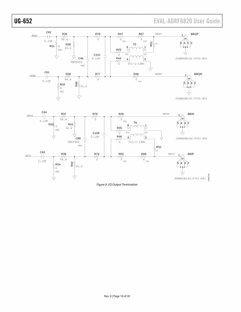
QUADRATURE I/Q OUTPUTS On the evaluation board, the quadrature I/Q outputs are ter-minated with 200 Ω differential. This is achieved by using a 1:1 transformer and an L-impedance matching network. The 1:1 transformer, TC1-1-13M+ from Mini-Circuits, is a very wide bandwidth (4.5 MHz to 3000 MHz) transformer that allows a flat pass-band response of up to 1 GHz. Using a wide bandwidth transformer is necessary to accurately evaluate the wideband pass-band response of the ADRF6820 without the effects of the
transformer/balun roll-off. However, to terminate the ADRF6820 with 200 Ω and also match the output impedance of the transformer with 50 Ω, an L network is placed between the I/Q outputs and the transformer. This introduces some power loss because the L network acts as a voltage divider (see Figure 3). The power loss due to the L network is approximately 17 dB.
5 4
1BBIP1
3 2
BBIPBBIP
JOHNSON142-0701-851
C630.1µF
R340ΩDNI
R4232.4Ω
R3886.6Ω
R500ΩDNI
R680ΩDNI
TC1-1-13M+4 3
R460Ω R52
0Ω
5 4
1BBIN1
3 2
BBINBBIN
JOHNSON142-0701-851
C640.1µF
R330ΩDNI
R4132.4Ω
R3786.6Ω
R490ΩDNI
6 1
PRI SEC
T6
R450Ω
1199
3-00
3
Figure 3. I/Q Output Matching Network
To avoid the power loss from the L network while achieving the proper impedance matching, a 4:1 impedance transformer, such as the TC4-1W+ from Mini-Circuits can be used in place of the TC1-1-13M+. This 4:1 impedance transformer allows the primary side of the transformer to be terminated with 200 Ω and the secondary side to be terminated with 50 Ω. The L network then becomes unnecessary and can be shorted out by replacing R35, R36, R37, and R38 with 0 Ω while R31, R32, R33, R34, R39, R40, R41, and R42 can all be DNI (do not install). Attention needs to be paid to the bandwidth of the transformer because impedance transformation transformers tend to have narrower bandwidths. The TC4-1W+ has a listed bandwidth of 3 MHz to 800 MHz; however, the 1 dB bandwidth is limited to 100 MHz. As a result, the roll-off of the transformer may distort the pass-band flatness of the ADRF6820, depending on which bandwidth configuration is used for the ADRF6820.

EVAL-ADRF6820 User Guide UG-652
Rev. 0 | Page 5 of 20
EVALUATION BOARD CONTROL SOFTWARE The ADRF6820 evaluation board is configured with a USB friendly interface to allow programmability of the ADRF6820 registers.
SOFTWARE INSTALLATION PROCEDURES The following instructions describe how to install the ADRF6820 control software, as well as the Cypress generic USB driver, on a computer running a Windows XP, Windows Vista, or Windows 7 (32- or 64-bit) operating system.
Warning
Install the necessary software before plugging the USB cable into the computer.
Installing the Evaluation Software
1. From the extracted folder, ADI_RFG_Drivers, double-click the ADI_RFG_Drivers.exe file. Running this file allows the installation of the Cypress CyUSB.sys driver as a verified, signed driver.
2. From the extracted .zip file, double-click the ADRF6820_ install.exe file. An icon should appear on your desktop with the ADI logo, titled ADRF6820.
3. After the installer is finished, install the USB driver.
Installing the Driver
1. Connect the USB connector on the evaluation board to the PC using the USB cable that was included in the box.
2. In either Windows XP or Windows Vista, right-click My Computer and then select Properties.
3. Open the Device Manager. a. In Windows Vista or Windows 7, select the Device
Manager option. b. In Windows XP, select the Hardware tab and then
click Device Manager. 4. In Device Manager, select the last category, Universal
Serial Bus Controllers. You should see an entry that either
has a yellow flag (indicating an unknown device) or an entry labeled ADF4xxx USB Driver (if you have installed a previous ADRF6x0x or ADI Limerick PLL software).
5. Right-click on the appropriate device and select update driver. 6. Browse to select the directory C:\Program Files\
ADRF6820_customer_software. 7. Click Next. Windows completes the driver installation.
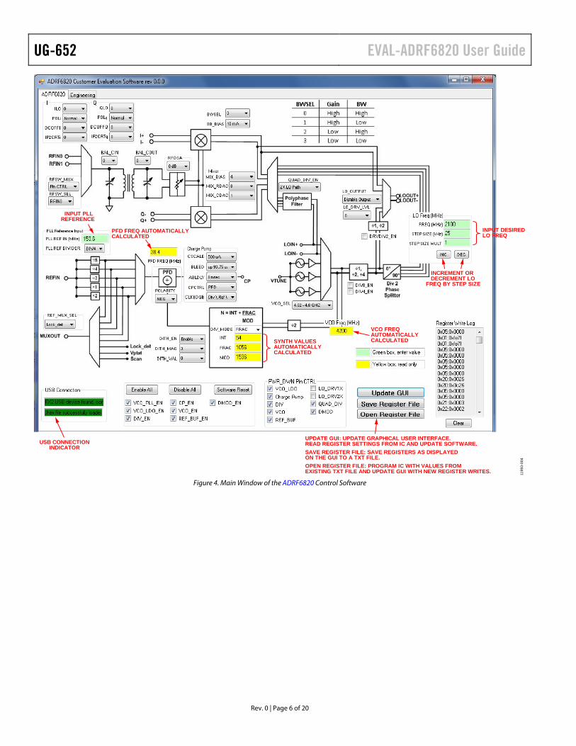
USING THE ADRF6820 EVALUATION SOFTWARE ADRF6820 Tab
The main window of the ADRF6820 evaluation software includes a block diagram that shows how the registers affect the major functional blocks of the ADRF6820 (see Figure 4). Within this window, the green boxes indicate that user input is required, and the yellow boxes indicate read only information.
To use the ADRF6820 evaluation software,
1. Before reading or writing to the registers, validate the USB connection by reading the USB indicators located in the lower left corner of the main window.
2. Click Update GUI to read the register values from the device and update the user interface. (An automatic write to the chip is initiated every time a register value is changed from the user interface.)
3. Specify the PLL reference and the desired LO frequency by typing the appropriate values into the designated boxes. Press ENTER after each input, and the software (via the PLL synthesizer blocks) calculates and sets the INT, FRAC, and MOD values accordingly.
Engineering Tab
The Engineering tab (see Figure 5) allows specific reads and writes to individual registers. Be sure to type values into the Address (decimal) and Write Data (decimal) boxes in decimal format.
UG-652 EVAL-ADRF6820 User Guide
Rev. 0 | Page 6 of 20
USB CONNECTIONINDICATOR
SYNTH VALUESAUTOMATICALLYCALCULATED
VCO FREQAUTOMATICALLYCALCULATED
INPUT DESIREDLO FREQ
INCREMENT ORDECREMENT LO
FREQ BY STEP SIZE
INPUT PLLREFERENCE
PFD FREQ AUTOMATICALLYCALCULATED
UPDATE GUI: UPDATE GRAPHICAL USER INTERFACE.READ REGISTER SETTINGS FROM IC AND UPDATE SOFTWARE.SAVE REGISTER FILE: SAVE REGISTERS AS DISPLAYEDON THE GUI TO A TXT FILE.OPEN REGISTER FILE: PROGRAM IC WITH VALUES FROMEXISTING TXT FILE AND UPDATE GUI WITH NEW REGISTER WRITES. 11
993-
004
Figure 4. Main Window of the ADRF6820 Control Software

EVAL-ADRF6820 User Guide UG-652
Rev. 0 | Page 7 of 20
1199
3-00
5
Figure 5. Engineering Tab of the ADRF6820 Control Software

UG-652 EVAL-ADRF6820 User Guide
Rev. 0 | Page 8 of 20
EVALUATION BOARD SCHEMATICS AND ARTWORK
1199
3-00
8
NOTE: EITHER T1 OR T2 PLACED (DUAL FOOTPRINT)
NOTE: EITHER T3 OR T4PLACED (DUAL FOOTPRINT)
23
1P3
R91
R90
25
98
32
24
11
31
13 15
32
12
21
36
30
19
1
14 20
22
29
39PAD
16 17 18
35 3438
28
26
23
27
33
10
40 37
76
45
U5
C86
6
4
513
2
Y2
R20R19
R18R17
DECL_VCO2
R63R62
R72 5 4 3 2
1 LO_IP
R70
R71
R55
R57
R69
R16
R15
C67
R65
R64
C69
L6
C71
L8
C73
L10
5 4 3 2
1 LOON
5 4 3 2
1 LOOP
C68 C72
L9L7
C70
L5
R6
R54312
S1
R30
MUXOUT
AC
CR1
VOCM
C35 C37
R29
C38
5432
1
REF_IN
6
43
1T4
5 4 3 2
1 LO_IN
C51
C52
1
62 5
4
3
T3
T2
1
62 5
4
3
T1
C48C41
C42 C43
C49C47
C53 C56
C46 C50
C55
C54
C44C40
C39
C34C31
C36
C3 C14
C9 C13 C16
DECL_2P5V
5 4 3 2
1 RF1
5 4 3 2
1 RF0
GND4GND3GND2GND1
C25
C24
0
0.1UFC0402
DIG_3P3V
0.1UF
DNI
DNI
BLK
DNI
1.00K
TBD0402DNI
YEL
LO_3P3V
100PF
10UF
0.22UF
0
DNI
3600BL14M050
VPRF_+5V0
0.1UF
DNI
1000PF
0
142-0701-201
LO_ON
VPMX_+5V
LOIN
0
100PF
DIG_3P3V
0
EG1218
LOON1
0.1UF
0.1UF
100PF
DNI
0.1UF
SML-210MTT86
YEL
LOOP1
100PF
LO_IP
0
DNI
DNI0
TBD0402
DNI
TC1-1-43A+
DNI
DNI
JOHNSON142-0701-851
0
YEL
100PF0
TBD0402
DNI
DNITBD0402
TBD0402
DNITBD0402
TBD0402DNI
DNI
TBD0402
3600BL14M050
DNI0
0
TBD0402
DNITBD0402
100PF
0
YEL
BBQN
BBQP
SCLK
LOOP
LOON
RFIN1
RFIN0
VTUNE
CPOUT
SDIO
CSB
PWRDWN
C0402
0.1UF 100PF
0
0
DIG_3P3V
100PF
DECL_VCO
PLL_3P3V
0.1UF
49.9
1000PF
100PF
100PF
LOIP
C0402
VCO_3P3V
100PF
TC1-1-43A+
142-0701-201
100PF
38.4MEGHZ
100PF
10UF
10UF
TBD0402
TBD0402
TBD0402
10UF
ADRF6820ACPZ
5.1K
5.1K
100PF
JOHNSON142-0701-851
10UF
VCC_+3P3V
LO2_3P3V
BLK
LO_IN
JOHNSON142-0701-851
0 0DNI
LO_OUT
LO_OP
1000PF
3PIN_SOLDER_JUMPER
BBIN
BBIP
JOHNSON142-0701-851
0
JOHNSON142-0701-851
BLK BLK
BCOM
A
NC
GNDGND
GNDGND
PWRDWN
VCC
_3P3
CSB
SDIO
VCC
_5V
GN
D
VCC
_3P3
VCC_3P3
GND
GND
GND
VCC_5V
VCC
_3P3
VCC_3P3
PAD
DEC
L_2P
5R
EFIN
CPO
UT
LOIP
LOIN
DEC
L_VC
OVT
UN
E
RFIN0
DECL_VCO2
RFIN1
RFS
W0
LOO
NLO
OP
MU
XOU
T
SCLK
VOC
M
DECL_MX
BBQPBBQNBBINBBIP
ENABLE/DISABLE_N
VCC
NC
OUTPUT
GND
SEC PRI
NC_6
BAL_OUT1
BAL_OUT2GND_DC_FEED_RFGND
UNBAL_IN
GND
SEC PRI
NC_6
BAL_OUT1
BAL_OUT2GND_DC_FEED_RFGND
UNBAL_IN
GND
Figure 6. ADRF6820 Schematic

EVAL-ADRF6820 User Guide UG-652
Rev. 0 | Page 9 of 20
1199
3-00
9
R21PWRDWNVCC_+3P3V
PWRDWN0
EG1218
Figure 7. Power-Down Switch
1199
3-01
5R88
R89
R74
R75
VTUNE
R56
DECL_VCO
CP
R11
C57 C60C59
C58
R23
R12
R26
0
3K
YEL
CPOUT
22PF
0
YEL
10KVTUNE
22PF
2.7NF
10K
6.8PF
0
YEL
0
0
0DECL_VCO
DNI
Figure 8. External Loop Filter
UG-652 EVAL-ADRF6820 User Guide
Rev. 0 | Page 10 of 20
1199
3-01
4
C88
C108
R79
R78 R49
R50 R68
R52
R46
R45
R42
6
4 3
1T6
5 4 3 2
1 BBIP
5 4 3 2
1 BBIN
R41
R34
C63 R38
R37
R33
C64
DNI
0
0
0.1UF
32.4
BBIP
BBIN
DNI
0
0.1UF
0DNI
0.1UF
86.6
86.6
32.4
0DNIDNI
BBIN1
0DNI
BBIP1
0
0
JOHNSON142-0701-851
0
0
JOHNSON142-0701-851
TC1-1-13M+TBD0402
SECPRI
C45C101
R77
R76
R48
R67R47
R32
C61
R31
C62
R36R
40
R35
R39
R43
R44
6
4 3
1T5
5 4 3 2
1 BBQN
R51 5 4 3 2
1 BBQP
DNI
TBD0402
0
0.1UF
86.6
86.6
0
0
0.1UF
DNI
BBQN1
DNI
32.4
JOHNSON142-0701-851
BBQN
BBQP
DNI
0
0.1UF0
DNI
0
0
BBQP1
0
DNI
JOHNSON142-0701-851
0
32.4
0
TC1-1-13M+
SECPRI
Figure 9. I/Q Output Termination

EVAL-ADRF6820 User Guide UG-652
Rev. 0 | Page 11 of 20
1199
3-01
0
330PF330PF
330PF
DECOUPLING FOR U1
1SDIO
1CSB
1SCLK
R25
A C
CR2R8R28
R24
R10
R9
C12 R13 C27 R14 C28
4
5
44
554332271711
1615
42
14
21
52515049484746452524232221201918
PAD
4039383736353433
13
565341282612
89
31302954
73106
U1
C20 C21 C22 C23 C15 C17 C26
R4A C
D1
R1 C16
PAD
21
87
5
3
U3
R3
C2 R2 C18
7
8
56
4
321
U2 R5
C6 C7
R27 R7
C19
C8
54321
G4G3G2G1
P1
C10
31
42
Y1
C11
C5
C4
YEL
DGND
DGND
DGND
DGND
DGND
DGND
DGND
DGND
DGND
ADP3334ACPZ
1000PF 140K
XTALOUT
PA3
CY7C68013A-56LTXC
JEDEC_TYPE=QFN56_8X8_PAD5_2X4_5
SDIO
CSB
24.000000MEGHZ
SCLK
YEL
SML-210MTT862K
PA0PA1PA2
5V_USB
5V_USB
0
1.00K
3V3_USB
DNI100K
1UF
1UF
SCL
WAKEUP
RESETN
SDA
DM
22PF
DNI
TBD0402 TBD0402
DNI
0
0
DNI
10PF
DP
E013815
FB
78.7K
2K
SML-210MTT86
2K
0
10PF
DNI1.00K
DNI1.00K
DNITBD0402
22PF
XTALIN
897-43-005-00-100001
3V3_USB
2K
IFCLK
CTL0_FLAGACLKOUT
CTL2_FLAGC
PA4PA5PA6
PB1PB0
PB3PB2
PB6PB5
PB7
PD1PD0
PD3PD2
PD6PD5PD4
PD7
PA7
0.1UF
0.1UF
0.1UF0.1UF
0.1UF0.1UF0.1UF0.1UF0.1UF0.1UF
TBD0603
24LC64-I-SN
0.1UF
PB4
CTL1_FLAGB
YEL
OUT
OUT
OUT
PINSGND
OUT
CASE
PAD
CLKOUT
PD7_FD15PD6_FD14PD5_FD13PD4_FD12PD3_FD11PD2_FD10
PD1_FD9PD0_FD8
WAKEUP
RESET_N
PA7_FLAGD_SLCS_NPA6_PKTEND
PA5_FIFOADR1PA4_FIFOADR0
PA3_WU2PA2_SLOE
PA1_INT1_NPA0_INT0_N
VCC
CTL2_FLAGCCTL1_FLAGBCTL0_FLAGA
GND
PB7_FD7PB6_FD6PB5_FD5PB4_FD4PB3_FD3PB2_FD2PB1_FD1PB0_FD0
SDASCL
RESERVED
IFCLKDMINUS
DPLUS
AGND
XTALIN
XTALOUTAVCC
RDY1_SLWRRDY0_SLRD
IN
IO
IN1IN2 OUT2
OUT1
PADFB
GNDSD_N
D
GND
SCL SDAWC_N
A2A1A0
VCC
IN
IN
IN
OUT
OUT
OUT
OUT
OUT
OUT
OUT
OUT
OUT
OUT
OUT
OUT
OUT
OUT
OUT
OUT
OUT
OUT
OUT
OUT
OUT
OUT
OUT
OUT
OUT
Figure 10. Serial Port Schematic

UG-652 EVAL-ADRF6820 User Guide
Rev. 0 | Page 12 of 20
1199
3-01
1
(FROM MAIN BOARD; 200MA MINIMUM)15V_SDP
TP2
TP3TP1 R86
R87
R85
R84
R83
R80 R81
R827
4
8
56321
U11
605958575655545352515049484746454443424140393837363534333231302928272625242322212019181716151413121110987654321
P2
616263646566676869707172737475767778798081828384858687888990919293949596979899
100101102103104105106107108109110111112113114115116117118119120
P2
SCLK
SDIO
CSB
0 DNI
DNI
0
DGND
DGND DGND
100K
100K
DNI
24LC32A-I/MS
JEDEC_TYPE=MSOP8E014160
FX8-120S-SV(21) FX8-120S-SV(21)
0
DNI0
0
YEL
5V_SDP
TBD0603
DNI
VSS
VCC
WP
A2A1A0
SCLSDA
Figure 11. SDP Connector

EVAL-ADRF6820 User Guide UG-652
Rev. 0 | Page 13 of 20
1199
3-01
2
REPLACE WITH COILCRAFT INDUCTOR - EPL2014
16
PAD52 3
4
U4
GND5
L11
21E2
E6
E7
E1
E5
E4
E3
VCC_VPMX
23
1JP7
23
1
JP8
321
JP5
321
JP3
R66
R73
21
P5
21+6V 1
+6V_TP
C100
C99
R58
C77
C76
C32
C75
C104
C105
R59
C106
C98C78
5
4
1
2
3
U8
C103C96C94
L12
R53
C102C97
L1
L2
L4
L3
R22
2
1
3 Q1
C95C84
2 31
JP2
1
4
78
62
5
PAD
3
U10
R61
C93
C91321
JP6
321
JP4
R60
2 31
JP1
C92
1
4
78
62
5
PAD
3
U9
VCC_+3P3V
VCC_+5V
C82
C83 C89
U6
C81
C80
C79 C85
C33 C66
C30
C29
1827
PAD
46 35
U7
C74
C65
C90
ADP151ACPZ-3.3-R7
NDS331NADP121-AUJZ33R7
SAMTECTSW10608GS3PIN
BLK
RED
3PIN_SOLDER_JUMPER
3PIN_SOLDER_JUMPER
ADP2370ACPZ-3.3
ADP2370ACPZ-5.0
ADP7104ACPZ-5.0-R7
22-03-2031
0.1UF
SW_+5V
10UH
22UF22UF
VCC_+3P3V
LO2_3P3V
120OHMLO_3P3V
DIG_3P3V
120OHM
1UF
1UF
1UF
10UF
0.1UF0.1UF
6.8UH
4.02K
1UF
22UF
22UF22UF 22UF
VPRF_+5V
VCO_3P3V
1UFDNI
571-0100
10K
1UF
+6V
1UF
22-03-2031
4.02K
SAMTECTSW10608GS3PIN
APD121_3V3
VCC_+5V
571-0500
1UF
10UH
10UF
1UH 10K
1.2
3PIN_SOLDER_JUMPER
1UF
1.2
10UF
1UH
10UF
DNI
10K
3PIN_SOLDER_JUMPER
10UF 1UF
LDO_+5V
SW_3V3
LDO_3V3
RED
ADP151_3V3
ADP7104ACPZ-3.3-R7
1UF
VPMX_+5V
RED
1UF
22UF
DNI
1UF10UF
22UF
6.8UH
22UF
0
PLL_3P3V
100UF
VCC_+3P3V
1UF
120OHM
120OHM
120OHM
120OHM
120OHM
RED
1UF0.1UF
SENSE
PAD
VINPGGNDEN NC
GND
VOUT
SENSE
PAD
VINPGGNDEN NC
GND
VOUT
PAD
VINEN
GNDNC
VOUT
BCOM
A
BCOM
A
GNDNC4
OUTENIN
G
S
D
BC
OMA
EPADPGND
SWPGFBSYNC
ENFSELVIN
BC
OMA
EPADPGND
SWPGFBSYNC
ENFSELVIN
Figure 12. Power Management
UG-652 EVAL-ADRF6820 User Guide
Rev. 0 | Page 14 of 20
1199
3-00
6
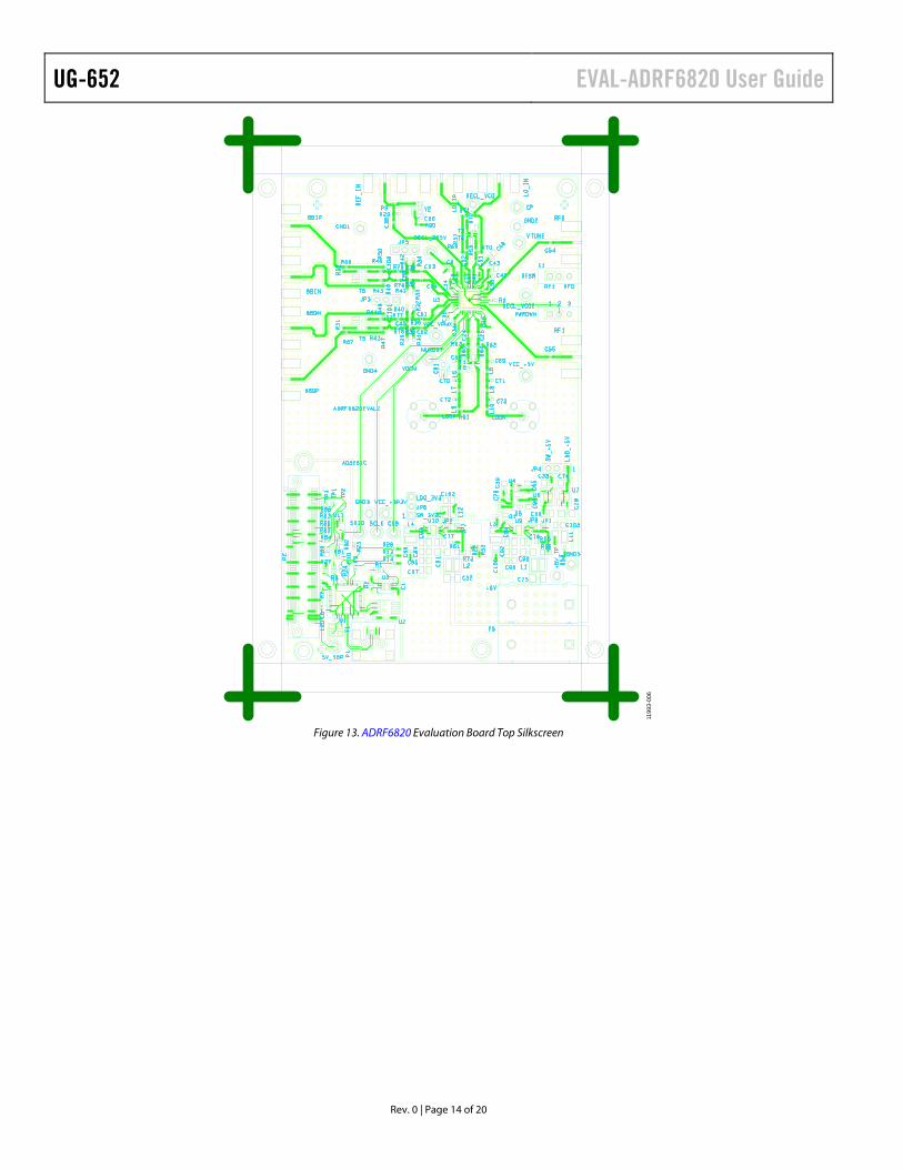
Figure 13. ADRF6820 Evaluation Board Top Silkscreen

EVAL-ADRF6820 User Guide UG-652
Rev. 0 | Page 15 of 20
1199
3-00
7
Figure 14. ADRF6820 Evaluation Board Bottom Silkscreen

UG-652 EVAL-ADRF6820 User Guide
Rev. 0 | Page 16 of 20
BILL OF MATERIALS Table 1. ADRF6820 Evaluation Board Bill of Materials Qty Reference Designator Description Manufacturer Manufacturer Part No. 1 +6V Connector-PCB single socket red,
CNDELTRON-571 Deltron 571-0500
4 +6V_TP, VCC_+5V, VCC_VPMX, VCC_+3P3V
Connectors-PCB test point red, CNLOOPTP Components Corporation TP-104-01-02
11 CP, CSB, SCLK, SDIO, VOCM, VTUNE, 5V_SDP, MUXOUT, DECL_VCO, DECL_2P5V, DECL_VCO2
Connectors-PCB test point yellow, CNLOOPTP
Components Corporation TP-104-01-04
9 RF0, RF1, BBIN, BBIP, BBQN, BBQP, LO_IN, LO_IP, REF_IN
Connectors-PCB coax SMA end launch, CNJOHNSON142-0701-851
Johnson 142-0701-851
2 C1, C18 Capacitor monolithic ceramic X5R, 1 µF, 10%, 25 V, C0603
Murata GRM188R61E105KA12D
2 C10, C11 Capacitor ceramic NP0, 22 pF, 5%, 50 V, C0603
Phycomp (Yageo) CC0603JRNP09BN220
4 C85, C89, C99, C100 Capacitor ceramic X7R 0805, 0.1 µF, 10%, 25 V, C0805
Murata GRM21BR71E104KA01L
23 C3, C5 to C7, C13, C15, C17, C19 to C23, C26, C31, C35, C39, C44, C56, C61 to C64, C86
Capacitor ceramic X7R 0402, 0.1 µF, 10%, 16 V Murata GRM155R71C104KA88D
9 C84, C92 to C97, C102, C103
Capacitor ceramic chip, 22 µF, 20%, 6.3 V, C0805
Murata GRM21BR60J226ME39L
2 C9, C104 Capacitor ceramic X5R 0603, 10 µF, 20%, 6.3 V Murata GRM188R60J106ME47D 1 C105 Capacitor ceramic X5R, 100 µF, 20%, 6.3 V,
C1206H71 Murata GRM31CR60J107ME39L
6 C79 to C83, C106 Capacitor monolithic ceramic 0402 SMD X5R, 1 µF, 10%, 10 V, C0402
Murata GRM155R61A105KE15D
14 C14, C16, C24, C25, C34, C37, C40 to C42, C46, C47, C51 to C53
Capacitor chip monolithic ceramic C0G 0402, 100 pF, 5%, 50 V, C0402
Murata GRM1555C1H101JD01D
1 C2 Capacitor ceramic C0G 0603, 1000 pF, 5%, 100 V, C0603
TDK C1608C0G2A102J
5 C29, C32, C75, C90, C91 Capacitor ceramic monolithic X5R, 10 µF, 10%, 25 V, C1206
Murata GRM31CR61E106KA12L
9 C30, C33, C65, C66, C74, C76 to C78, C98
Capacitor ceramic 0805 X7R, 1 µF, 10%, 16 V, C0805
Murata GRM21BR71C105K
1 C36 Capacitor ceramic Y5V, 0.22 µF, −20%, +80%, 16 V, C0402
Murata GRM155F51C224ZA01D
3 C38, C54, C55 Capacitor ceramic C0G 0402, 1000 pF, 5%, 50 V, C0402
Murata GRM1555C1H102JA01
2 C4, C8 Capacitor ceramic multilayer NP0 0402, 10 pF, 5%, 50 V, C0402
Phycomp (Yageo) CC0402JRNP09BN100
4 C43, C48 to C50 Capacitor ceramic monolithic, 10 µF, 10%, 16 V, C0805
Murata GRM21BR61C106KE15L
2 C57, C60 Capacitor ceramic, 22 pF, 5%, 50 V, C0402 Phycomp (Yageo) 0402CG220J9B200 1 C58 Capacitor ceramic monolithic, 2.7 nF, 5%, 50 V,
C0805 Murata GRM2165C1H272JA01D
1 C59 Capacitor ceramic NP0, 6.8 pF, 5%, 50 V, C0603
Phycomp (Yageo) 2238 867 15688
3 D1, CR1, CR2 LED 570 nm WTR clear 0805 SMD (green), 2.2 V, LED0805
Rohm Semiconductor SML-210MTT86
7 E1 to E7 Bead core chip, 120 Ω, L0603 Panasonic EXC-3BP121H 5 GND1 to GND5 Connectors-PCB test point black,
CNLOOPTP Components Corporation TP-104-01-00

EVAL-ADRF6820 User Guide UG-652
Rev. 0 | Page 17 of 20
Qty Reference Designator Description Manufacturer Manufacturer Part No. 2 JP3, JP5 Connectors-PCB wire to board hardware,
CNMOLEX22-03-2031 Molex 22-03-2031
2 JP4, JP6 Connectors-PCB BERG header ST male 3-pin, CNBERG1X3H205LD36
Samtec TSW-103-08-G-S
2 L1, L2 Inductor SMT power, 1 µH, 20%, LSML126W110H95
Coilcraft ME3220-102MLB
2 L3, L11 Inductor SMT power, 10 µH, 10%, LSML126W110H95
Coilcraft ME3220-103KLB
2 L4, L12 Inductor SMT power, 6.8 µH, 20%, LSML126W110H95
Coilcraft ME3220-682MLB
2 LOON, LOOP Connectors-PCB coax SMA ST, CNJOHNSON142-0701-201
Johnson 142-0701-201
1 P1 Connector-PCB receptacles mini-USB Type B SMT, CNTYCO-1734035-2
Mill-Max 897-43-005-00-100001
1 P2 Connector-PCB vertical type receptacles SMD, CNHRSFX8-120S-SV
Hirose FX8-120S-SV(21)
1 P5 Connector-PCB single socket black, CNDELTRON-571
Deltron 571-0100
2 S1, PWRDWN SW PC mount slide switch, SWEG1218 E-Switch EG1218 1 Q1 Transistor N-channel LLE mode FET, SOT23 Fairchild NDS331N 4 R1, R4, R5, R8 Resistor film SMD 0603, 2 kΩ, 1%, 1/10 W,
R0603 Phycomp (Yageo) 9C06031A2001FKHFT
35 R6, R9 to R11, R17 to R21, R24, R25, R43 to R46, R51, R52, R54 to R57, R59, R64, R65, R72, R74, R76 to R79, R87 to R91
Resistor film SMD 0402, 0 Ω, 5%, 1/16 W, R0402
Panasonic ERJ-2GE0R00X
1 R12 Resistor thick film chip, 3 kΩ, 5%, 1/16 W, R0402
Panasonic ERJ-2GEJ302X
2 R15, R16 Resistor film SMD 0402, 5.1 kΩ, 5%, 1/16 W, R0402
Multicomp CR10B512JT
1 R2 Resistor precision thick film chip 0603, 140 kΩ, 1%, 50 V, 1/10 W, R0603
Panasonic ERJ-3EKF1403V
2 R23, R26 Resistor precision thick film chip R0402, 10 kΩ, 1%, 1/16 W, R0402
Panasonic ERJ-2RKF1002X
3 R27, R80, R82 Resistor precision thick film chip, 100 kΩ, 1%, 50 V, 1/10 W, R0603
Panasonic ERJ-3EKF1003V
1 R29 Resistor ultra-precision ultra-reliability MF chip, 49.9 Ω, 0.1%, 1/16 W, R0402
Susumu RG1005P-49R9-B-T5
1 R3 Resistor precision thick film chip 0603, 78.7 kΩ, 1%, 50 V, 1/10 W, R0603
Panasonic ERJ-3EKF7872V
1 R30 Resistor precision thick film chip R0402, 1.00 kΩ, 1%, 1/10 W, R0402
Panasonic ERJ-2RKF1001X
4 R35 to R38 Resistor chip SMD 0402, 86.6 Ω, 1%, 1/16 W, R0402
Panasonic ERJ-2RKF86R6X
4 R39 to R42 Resistor precision thick film chip R0402, 32.4 Ω, 1%, 1/16 W, R0402
Panasonic ERJ-2RKF32R4X
2 R53, R58 Resistor precision thick film chip 4.02 kΩ, 1%, 1/16 W, R0402
Panasonic ERJ-2RKF4021X
2 R66, R73 Resistor thick film chip, 1.2 Ω, 5%, 1/8 W, R0805
Panasonic ERJ-6GEYJ1R2V
2 T2, T4 Transformer RF SMT, AT224-1 Mini-Circuits TC1-1-43A+ 2 T5, T6 Transformer RF 1:1, AT224-1 Mini-Circuits TC1-1-13M+ 1 U1 IC HS USB peripheral, 3 V to 3.6 V,
QFN56_8X8_PAD5_2X4_5 Cypress Semiconductor CY7C68013A-56LTXC
1 U10 IC low quiescent current buck regulator 3.3 V output, QFN8_3X3_PAD2_44X1_7
Analog Devices ADP2370ACPZ-3.3
1 U11 IC 32-kbit serial EEPROM, MSOP8 Microchip 24LC32A-I/MS

UG-652 EVAL-ADRF6820 User Guide
Rev. 0 | Page 18 of 20
Qty Reference Designator Description Manufacturer Manufacturer Part No. 1 U2 IC 64-kbit EEPROM, SO8 Microchip 24LC64-I-SN 1 U3 IC high ACC, low quiescent current
adjustable low drop regulator, QFN8_3X3_PAD1_75X1_45
Analog Devices ADP3334ACPZ
1 U4 IC CMOS linear regulator LDO 3.3 V, DFN6_2X2_PAD1_6X1
Analog Devices ADP151ACPZ-3.3-R7
1 U5 IC wideband demodulator, QFN40_6X6_PAD4_6X4_6
Analog Devices ADRF6820ACPZ
1 U6 IC low noise, CMOS LDO, QFN8_3X3_PAD2_44X1_7
Analog Devices ADP7104ACPZ-3.3-R7
1 U7 IC low noise, CMOS LDO, QFN8_3X3_PAD2_44X1_7
Analog Devices ADP7104ACPZ-5.0-R7
1 U8 IC 150 mA, CMOS linear regulator, 2.3 V to 5.5 V, TSOT-5
Analog Devices ADP121-AUJZ33R7
1 U9 IC low quiescent current buck regulator 5.0 V output, QFN8_3X3_PAD2_44X1_7
Analog Devices ADP2370ACPZ-5.0
1 Y1 IC crystal SMD, 24.000000 MHz, XTALNX3225
NDK NX3225SA-24.000000MHZ
Table 2. ADRF6820 Evaluation Board Bill of Materials—Do Not Install1 Qty Reference Designator Description Manufacturer2 Manufacturer Part No. 12 C12, C27, C28, C45, C67 to
C73, C88, C101, C108 Do not install (TBD_C0402) N/A TBD0402
6 L5 to L10 Do not install (TBD_L0402) N/A TBD0402 3 R13, R14, R28 Resistor precision thick film chip R0402,
1.00 kΩ, 1%, 1/10 W Panasonic ERJ-2RKF1001X
3 R22, R60, R61 Resistor thick film chip, 10 kΩ, 5%, 1/10 W Panasonic ERJ-2GEJ103X 20 R31 to R34, R47 to R50, R62,
R63, R67 to R71, R75, R83 to R86
Resistor film SMD 0402, 0 Ω, 5%, 1/16 W Panasonic ERJ-2GE0R00X
2 R7, R81 Do not install (TBD_R0603) N/A TBD0603 2 T1, T3 Transformer 3.6 GHz balun Johanson Technology 3600BL14M050 1 Y2 IC crystal oscillator, 38.4 MHz, 3.3 V,
YSML98W79H35_A Rakon IT2200AQ
1 These components are part of the printed circuit board (PCB) or should not be installed. 2 N/A = not applicable.

EVAL-ADRF6820 User Guide UG-652
Rev. 0 | Page 19 of 20
NOTES

UG-652 EVAL-ADRF6820 User Guide
Rev. 0 | Page 20 of 20
NOTES
ESD Caution ESD (electrostatic discharge) sensitive device. Charged devices and circuit boards can discharge without detection. Although this product features patented or proprietary protection circuitry, damage may occur on devices subjected to high energy ESD. Therefore, proper ESD precautions should be taken to avoid performance degradation or loss of functionality.
Legal Terms and Conditions By using the evaluation board discussed herein (together with any tools, components documentation or support materials, the “Evaluation Board”), you are agreeing to be bound by the terms and conditions set forth below (“Agreement”) unless you have purchased the Evaluation Board, in which case the Analog Devices Standard Terms and Conditions of Sale shall govern. Do not use the Evaluation Board until you have read and agreed to the Agreement. Your use of the Evaluation Board shall signify your acceptance of the Agreement. This Agreement is made by and between you (“Customer”) and Analog Devices, Inc. (“ADI”), with its principal place of business at One Technology Way, Norwood, MA 02062, USA. Subject to the terms and conditions of the Agreement, ADI hereby grants to Customer a free, limited, personal, temporary, non-exclusive, non-sublicensable, non-transferable license to use the Evaluation Board FOR EVALUATION PURPOSES ONLY. Customer understands and agrees that the Evaluation Board is provided for the sole and exclusive purpose referenced above, and agrees not to use the Evaluation Board for any other purpose. Furthermore, the license granted is expressly made subject to the following additional limitations: Customer shall not (i) rent, lease, display, sell, transfer, assign, sublicense, or distribute the Evaluation Board; and (ii) permit any Third Party to access the Evaluation Board. As used herein, the term “Third Party” includes any entity other than ADI, Customer, their employees, affiliates and in-house consultants. The Evaluation Board is NOT sold to Customer; all rights not expressly granted herein, including ownership of the Evaluation Board, are reserved by ADI. CONFIDENTIALITY. This Agreement and the Evaluation Board shall all be considered the confidential and proprietary information of ADI. Customer may not disclose or transfer any portion of the Evaluation Board to any other party for any reason. Upon discontinuation of use of the Evaluation Board or termination of this Agreement, Customer agrees to promptly return the Evaluation Board to ADI. ADDITIONAL RESTRICTIONS. Customer may not disassemble, decompile or reverse engineer chips on the Evaluation Board. Customer shall inform ADI of any occurred damages or any modifications or alterations it makes to the Evaluation Board, including but not limited to soldering or any other activity that affects the material content of the Evaluation Board. Modifications to the Evaluation Board must comply with applicable law, including but not limited to the RoHS Directive. TERMINATION. ADI may terminate this Agreement at any time upon giving written notice to Customer. Customer agrees to return to ADI the Evaluation Board at that time. LIMITATION OF LIABILITY. THE EVALUATION BOARD PROVIDED HEREUNDER IS PROVIDED “AS IS” AND ADI MAKES NO WARRANTIES OR REPRESENTATIONS OF ANY KIND WITH RESPECT TO IT. ADI SPECIFICALLY DISCLAIMS ANY REPRESENTATIONS, ENDORSEMENTS, GUARANTEES, OR WARRANTIES, EXPRESS OR IMPLIED, RELATED TO THE EVALUATION BOARD INCLUDING, BUT NOT LIMITED TO, THE IMPLIED WARRANTY OF MERCHANTABILITY, TITLE, FITNESS FOR A PARTICULAR PURPOSE OR NONINFRINGEMENT OF INTELLECTUAL PROPERTY RIGHTS. IN NO EVENT WILL ADI AND ITS LICENSORS BE LIABLE FOR ANY INCIDENTAL, SPECIAL, INDIRECT, OR CONSEQUENTIAL DAMAGES RESULTING FROM CUSTOMER’S POSSESSION OR USE OF THE EVALUATION BOARD, INCLUDING BUT NOT LIMITED TO LOST PROFITS, DELAY COSTS, LABOR COSTS OR LOSS OF GOODWILL. ADI’S TOTAL LIABILITY FROM ANY AND ALL CAUSES SHALL BE LIMITED TO THE AMOUNT OF ONE HUNDRED US DOLLARS ($100.00). EXPORT. Customer agrees that it will not directly or indirectly export the Evaluation Board to another country, and that it will comply with all applicable United States federal laws and regulations relating to exports. GOVERNING LAW. This Agreement shall be governed by and construed in accordance with the substantive laws of the Commonwealth of Massachusetts (excluding conflict of law rules). Any legal action regarding this Agreement will be heard in the state or federal courts having jurisdiction in Suffolk County, Massachusetts, and Customer hereby submits to the personal jurisdiction and venue of such courts. The United Nations Convention on Contracts for the International Sale of Goods shall not apply to this Agreement and is expressly disclaimed.
©2014 Analog Devices, Inc. All rights reserved. Trademarks and registered trademarks are the property of their respective owners. UG11993-0-2/14(0)