Edinburgh Research Explorer - COnnecting REpositories · be easily grown by vacuum sublimation ......
23
Edinburgh Research Explorer Planar Ni(II), Cu(II) and Co(II) tetraaza[14]annulenes: Structural, electronic and magnetic properties and application to field effect transistors Citation for published version: Whyte, AM, Shuku, Y, Nichol, GS, Matsushita, MM, Awaga, K & Robertson, N 2012, 'Planar Ni(II), Cu(II) and Co(II) tetraaza[14]annulenes: Structural, electronic and magnetic properties and application to field effect transistors' Journal of Materials Chemistry, vol 22, no. 34, pp. 17967-17975. DOI: 10.1039/c2jm33079b Digital Object Identifier (DOI): 10.1039/c2jm33079b Link: Link to publication record in Edinburgh Research Explorer Document Version: Peer reviewed version Published In: Journal of Materials Chemistry Publisher Rights Statement: Copyright © 2012 by the Royal Society of Chemistry. All rights reserved. General rights Copyright for the publications made accessible via the Edinburgh Research Explorer is retained by the author(s) and / or other copyright owners and it is a condition of accessing these publications that users recognise and abide by the legal requirements associated with these rights. Take down policy The University of Edinburgh has made every reasonable effort to ensure that Edinburgh Research Explorer content complies with UK legislation. If you believe that the public display of this file breaches copyright please contact [email protected] providing details, and we will remove access to the work immediately and investigate your claim. Download date: 28. Apr. 2017
Transcript of Edinburgh Research Explorer - COnnecting REpositories · be easily grown by vacuum sublimation ......
Edinburgh Research Explorer
Planar Ni(II), Cu(II) and Co(II) tetraaza[14]annulenes: Structural,electronic and magnetic properties and application to field effecttransistors
Citation for published version:Whyte, AM, Shuku, Y, Nichol, GS, Matsushita, MM, Awaga, K & Robertson, N 2012, 'Planar Ni(II), Cu(II)and Co(II) tetraaza[14]annulenes: Structural, electronic and magnetic properties and application to fieldeffect transistors' Journal of Materials Chemistry, vol 22, no. 34, pp. 17967-17975. DOI:10.1039/c2jm33079b
Digital Object Identifier (DOI):10.1039/c2jm33079b
Link:Link to publication record in Edinburgh Research Explorer
Document Version:Peer reviewed version
Published In:Journal of Materials Chemistry
Publisher Rights Statement:Copyright © 2012 by the Royal Society of Chemistry. All rights reserved.
General rightsCopyright for the publications made accessible via the Edinburgh Research Explorer is retained by the author(s)and / or other copyright owners and it is a condition of accessing these publications that users recognise andabide by the legal requirements associated with these rights.
Take down policyThe University of Edinburgh has made every reasonable effort to ensure that Edinburgh Research Explorercontent complies with UK legislation. If you believe that the public display of this file breaches copyright pleasecontact [email protected] providing details, and we will remove access to the work immediately andinvestigate your claim.
Download date: 28. Apr. 2017
Planar Ni(II), Cu(II) and Co(II) tetraaza[14]annulenes: Structural,
electronic and magnetic properties and application to field
effect transistors**
Alexander M. Whyte,1 Yoshiaki Shuku,
2 Gary S. Nichol,
1 Michio M. Matsushita,
2 Kunio Awaga
2
and Neil Robertson1,*
[1]EaStCHEM, School of Chemistry, Joseph Black Building, University of Edinburgh, West Mains Road,
Edinburgh, EH9 3JJ, UK.
[2]Department of Chemistry, Graduate School of Science, and Research Center of Materials Science, Nagoya
University, Chikusa-ku, Japan.
[*
]Corresponding author; e-mail: [email protected], fax: +44 (0)131 650 4743, tel: +44 (0)131 650 475
[**
]We thank the EPSRC (UK) and JST (Japan) for financial support through the joint EPSRC-JST
programme. This work has made use of the resources provided by the EaStChem Research Computing
Facility (http://www.eastchem.ac.uk/rcf). This facility is partially supported by the eDIKT initiative
(http://www.edikt.org). We also thank Christopher Cameron and the University of Edinburgh Crystallography
service for collecting crystallographic data and assistance solving crystal structures.
Supporting information: [†
] Electronic supplementary information (ESI) available. CCDC 882247–882250. For ESI and
crystallographic data in CIF or other electronic format see http://dx.doi.org/10.1039/C2JM33079B
Post-print of a peer-reviewed article published by the Royal Society of Chemistry.
Published article available at: http://dx.doi.org/10.1039/C2JM33079B
Cite as:
Whyte, A. M., Shuku, Y., Nichol, G. S., Matsushita, M. M., Awaga, K., & Robertson, N. (2012).
Planar Ni(II), Cu(II) and Co(II) tetraaza[14]annulenes: structural, electronic and magnetic
properties and application to field effect transistors. Journal of Materials Chemistry, 22(34), 17967-
17975.
Manuscript received: 15/05/2012; Accepted: 17/07/2012; Article published: 30/07/2012

Page 1 of 22
Abstract
A series of planar Ni(II), Cu(II) and Co(II) tetraaza[14]annulenes has been prepared and studied optically,
electrochemically and magnetically. Thin films of each of these complexes have been prepared by vacuum
deposition to evaluate the field-effect transistor (FET) performance as well as the morphology and
crystallinity of the film formed. The electrochemistry and UV/Vis absorption studies indicate the materials are
redox active and highly coloured, with molar extinction coefficients as large as 80,000 M-1
cm-1
in the visible
region. The paramagnetic complexes display weak antiferromagnetic interactions, fit to the Bonner-Fisher
chain model. Each of the materials formed polycrystalline films when vacuum deposited and showed field-
effect transistor behaviour, with charge carrier mobilities in the range of 10-5
to 10-9
cm2 V
-1 s
-1. SEM imaging
of the substrates indicates that the central metal ion, and its sublimation temperature, has a crucial role in
defining the morphology of the resulting film.
Introduction
Porphyrins and phthalocyanines represent some of the most promising candidates for a range of applications
due to their fascinating optical and electronic properties.1 These planar, π-conjugated macrocycles commonly
find widespread use as the semiconducting layer in field effect transistors,2-4
organic light emitting diodes5 and
as the light harvesting component in solar cells.6, 7
An attractive feature is the ability to functionalise the
periphery and/or incorporate a wide range of metal ions into the central cavity of these macrocycles, in order
to tune their physical, optical and electronic properties. In addition to its electronic effect, it has previously
been demonstrated that the size of the central metal ion can play a key role in the charge carrier mobility, by
dictating the intermolecular distance in the crystal lattice,8 with the smaller metal facilitating better overlap of
the ligand based frontier orbitals.
Although porphyrins have been utilised less in FETs compared with other organic electronic devices,9 these
molecules typically demonstrate p-type conductivity with respectable mobilities in the range of 10-6
to 10-1
cm2V
-1s
-1.4 Phthalocyanines on the other hand, have slightly higher reported mobilities in the range10
-3 to 1.0
cm2V
-1s
-1 depending on the central metal and the device specifications.
10, 11 An interesting feature of
phthalocyanine chemistry is that their semiconducting behaviour can be switched from p-type to n-type, going
from the unsubstituted compound to the hexadecafluorinated analogue.12, 13
Along with their attractive
qualities such as planarity, high number of π-electrons and suitable crystal packing, the high thermal and
chemical stability of these macrocycles is of importance in FET applications as this allows high purity films to
be easily grown by vacuum sublimation techniques.14
A well known, but less studied, porphyrin analogue is the class of dibenzotetraaza[14]annulenes.15
These
tetradentate ligands commonly bind metal ions in the dianionic form but complexes have also been reported

Page 2 of 22
from the neutral ligand.16
The geometry of the macrocycle can vary depending on the substituents on the 1,3-
propanediiminato linkage and the size of the metal ion in the central cavity.17
In the absence of any
substituents on the 1- or 3-positions of the propanediiminato moiety, then the free ligand is usually planar but
the introduction of methyl groups into these positions will disrupt this planarity, through steric interactions
with the benzene ring, and the ligand will adopt a buckled or saddle shaped conformation. Thus substituents
on the 1- or 3-positions of the propanediiminato linkage will result in marked changes in the solid state crystal
packing, which has important implications for conducting applications.
Figure 1. Structures of dibenzo[14]tetraazaannulene (H2L1) and dinaptho[14]teraazaannulene (H2L2).
In this work we have examined the electronic, magnetic, optical and charge transport properties of a series of
metal complexes using tetraazaannulene macrocyclic ligands (Figure 1). This class of macrocycle has been
previously shown to exhibit conductive behaviour when doped with iodine,18
but despite this, the thin film
charge transport properties have until now been unexplored.
Results and Discussion
1. Crystallography
The single crystal structure of Ni(L1) and the unit cell dimensions of Co(L1) have previously been reported19
and were shown to be isomorphous. Single crystals of Ni(L1) grown in our lab match the unit cell dimensions
previously reported. However, we have also grown crystals of Co(L1) and found the structure to be
orthorhombic rather than monoclinic as was previously reported along with the unit cell dimensions.19
Herein
we also report the single crystal structure of the analogous Cu(L1) complex and of Ni(L2). In addition, a
Co(III) complex, Co(L1)Cl, has been isolated by recrystallising Co(L1) from DCM and toluene (Table S1).
Unlike Ni(L1), the crystal structure of Co(L1) contains one molecule in its asymmetric unit. The molecules
are packed in a herringbone motif with short, equidistant 1-D interplanar distances of 3.240 Å. The π-stacking
is slipped with the propanediimine linkages overlapping effectively with a short contact of 3.29(2) Å, similar
to what is observed in Ni(L1) and Cu(L1) (vide infra). The geometry around the Co(II) centre is square planar,
as expected, with varying Co-N bond lengths of 1.896(11), 1.886(10), 1.836(11) and 1.870(10) Å. The N-Co-

Page 3 of 22
N bite angles are 84.7(7) and 87.0(6)°. The short contact between the Co(II) centre and the closest C atom on
the adjacent molecules is 3.45(1) Å indicating that a possible axial Co-C interaction could be present.
Unsurprisingly, the crystal structure of Cu(L1) is isomorphous to Ni(L1). The asymmetric unit contains two
crystallographically-independent Cu(L1) molecules, with each ligand coordinating Cu(II) in a square planar
manner. With regard to the environment around the metal centre, the first Cu(L1) molecule shows Cu-N
bonds of 1.926(2) and 1.927(2) Å, with the second molecule displaying Cu-N lengths of 1.927(2) and
1.928(1). These bonds are slightly longer than the Ni-N lengths of 1.869(2) and 1.872(2) Å, and 1.868(2) and
1.871(2) Å reported for Ni(L1).19
The N-Cu-N bite angles within the diaminobenzene fragment of 84.50(7)°
and 84.53(7)° are similar to the 85.25(8)° and 85.16(9)° reported in the case of Ni(L1). Similar to Co(L1), the
material crystallises in a herringbone fashion with short 1-D interplanar distances (3.238 Å) (Figure 3. The
planar, aromatic nature of the complexes combined with the short interplanar distances makes these molecules
suitable candidates for study as conducting materials. The molecules are π-stacked in a slipped fashion with
the propanediimine linkages overlapping, but with very little overlap of the aromatic rings (Figure 4). The
short contact between the Cu(II) centre and the closest C atom on the adjacent molecules at 3.468(2) Å is
similar to that observed in Co(L1).
← Figure 2. Structure of Co(L1). Displacement
ellipsoids are at the 50% probability level.
Figure 3. → Crystal packing of Cu(L1)
showing short interplanar distances.

Page 4 of 22
Figure 4. Molecular overlap of Cu(L1) as it stacks along the b-axis.
From the single crystal structure of Ni(L2) (Figure 5) it can be seen that, surprisingly, the increased π-
conjugation of the naphthalene ring has resulted in a non-planar structure. This non-planarity has resulted in a
larger face-to-face π-stacking distance (~6 Å) but the edge to face π-stacking distance is much shorter (~2.5
Å) (Figure 6). The non-planar structure may be a result of crystal packing forces, which have forced the
molecule to adopt a twisted geometry to minimise repulsive interactions between naphthalene rings. In
contrast to Cu(L1) and Ni(L1), the asymmetric unit of Ni(L2) contains only one molecule. The Ni-N distances
of 1.866(2) and 1.865(2), as well the N-Ni-N bite angle of 84.98(9)° indicate that the coordination
environment around the metal centre is almost identical to what was observed with Ni(L1).
Figure 5. The crystal structure obtained for Ni(L2).

Page 5 of 22
Figure 6. Crystal packing of Ni(L2).
The unit cell of Co(L1)Cl is shown in the supplementary information (Figure S1). The coordination geometry
around the Co(III) centre is square based pyramidal with the chloride ion bound in the axial position. In
contrast to Cu(L1) and Ni(L1), it appears that the metal centre in Co(L1) is susceptible to oxidation when to
left to crystallise in dichloromethane under an air environment over a period of a week. However, when in the
solid, powder form Co(L1) is air stable indefinitely. Solvent of crystallisation is also present in the unit cell; in
this case toluene is present in a 1:1 ratio with the complex, although the solvent has a high degree of disorder.
Since the complexes will be thermally evaporated onto substrates in the absence of solvent, the solid state
packing of Co(L1)Cl is not relevant in rationalising the FET performance.
2. Electrochemistry
Despite the poor solubility of these planar molecules, cyclic voltammetry (CV) measurements on L1 have
previously been reported,20
with the macrocycle displaying several electrochemically accessible redox
processes at -1.77, 0.75 and 1.06 V (vs. saturated calomel reference electrode). However, owing to the poor
solubility of the metallated macrocycles we found differential pulse voltammetry (DPV) to be a more useful
technique in the study of these materials due to its enhanced sensitivity. The effect of a metal centre on these
potentials is shown in Table 1. The differential pulse and cyclic voltammograms are given in the
supplementary information (Figure S6-S11,S13-S16).
Table 1. Redox potentials as measured by differential pulse from -2 to 1.8 V.
Sample Epc (V) Epa (V)
Co(L1) -1.07, -1.41, -1.62, -1.89 0.24, 0.79, 1.30, 1.51, 1.73
Cu(L1) -1.49 0.52, 1.08, 1.41
Ni(L1) -1.68 0.66, 1.38
Ni(L2) -1.67 0.46, 0.99, 1.72

Page 6 of 22
The cyclic voltammetry analysis of these complexes is hampered by the poor solubility of the macrocyclic
complexes, but in the case of Ni(L1), which appears to be the most soluble, some interesting behaviour was
observed. When the potential was scanned from 0 to 2 V, 2 to –2 V and then back to 0 V, two oxidations were
observed at positive potential, 0.72 and 1.40 V, and one reduction at negative potential, -1.77 V (Figure S11).
On repeating this scan a further four times, the reduction process disappears completely and the first oxidation
at 0.66 V grows in intensity. The second oxidation peak changes in shape after the second scan and appears at
a less positive potential; at 1.20 V by the fifth scan. This behaviour is indicative of a deposited film forming
on the working electrode and this was seen to be the case when the electrode was removed from solution
(Figure S12). In fact, the electrochemical polymerisation of similar compounds has already been reported.21, 22
Macrocycles of this type have previously been shown to first dimerise through the meso- position of the
propanediimine linkage, 23
before then undergoing further polymerisation under an applied potential. On
further studying Ni(L1) in the range –2 to 1 V we found that the oxidation and reduction potentials are largely
unchanged, except that the current associated with the reductive process is decreasing (Figure S13). The peak
potentials still occur in the same position, indicating that when scanning to this less positive potential the
sample is not polymerising, and that, although not electrochemically reversible, there is potentially some
chemical reversibility associated with the oxidation. The solubility of the other three complexes is lower than
that of Ni(L1), making meaningful analysis by CV challenging; peaks appear broad with little definition and
small peak current. Therefore, assessment of the reversibility of their redox processes becomes difficult.
In comparison to the other the complexes, Co(L1) displays many more redox processes when studied using
differential pulse voltammetry. This could be partly due to the facile nature of the Co(II) to Co(III) oxidation
but the number of additional processes could indicate the complex is decomposing or structurally changing.
As shown earlier (Figure S1) it is possible for Co(L1) to be oxidised to Co(L1)Cl in the presence of DCM,
thus it is plausible that additional redox processes could be the result of this species also existing in solution.
In summary, each of the materials displays at least two oxidations and one reduction, and these processes
appear to be electrochemically and mostly chemically irreversible. The electrochemistry however indicates
two important things, Firstly, in each of the complexes, with the exception of Co(L1), the frontier orbitals are
predominantly ligand based, shown by the similarity in redox processes between the Cu and Ni examples.
Secondly, due to the energies of the frontier orbitals the complexes are more suitable as electron donating
materials than electron acceptors in FET devices.
3. Magnetic Measurements
Susceptibility measurements were carried out on Cu(L1) and Co(L1) over the temperature range 1.8 – 300 K.
The data were fit to the Curie-Weiss law. For Cu(L1), the Curie constant obtained (Figure S18) of 0.392 cm3
K mol-1
is in good agreement with that expected for an S=1/2 paramagnet. A small, negative Weiss constant

Page 7 of 22
of -0.496(6) K was also obtained, suggesting weak antiferromagnetic exchange interactions. Analysis of the
crystal packing indicates that the Cu(L1) molecules stack as 1D, linear chains, therefore data were fit to the
modified Bonner-Fischer model, appropriate for linear chains of Heisenberg spins (H = -JΣSiSi+1),24
over the
range 1.8-300 K (Figure 7). From the experimental fitting, the following parameters were obtained; g of
2.04(1) and J of -0.4(1) cm-1
. The g value deviates from the free electron value indicating that, as we expect,
the unpaired electron is significantly metal based, and the small J value indicates the intermolecular magnetic
interaction is weak, consistent with the Curie-Weiss fit.
Figure 7. χT vs. T of Cu(L1) in black (lower curve), and Co(L1) in blue (upper curve). The curves of Cu(L1)
and Co(L1) have been corrected for temperature independent paramagnetic (TIP) contributions of 3.56 x10⁻⁴
cm3 mol
-1 and 2.61 x10
-4 cm
3 mol
-1, respectively. The solid red lines are the fits to the Bonner-Fisher model for
a linear chain of Heisenberg S = ½ centres.
In contrast to the Cu(II) analogue, the Curie-Weiss plot of Co(L1) (Figure S17) gives the Curie constant as
0.639(2) cm3 K mol
-1 and the Weiss constant as -3.2(1) K, suggesting the antiferromagnetic exchange
interaction is greater than in Cu(L1). Consistent with this, fit to the Bonner-Fisher model also indicates much
stronger magnetic coupling with a J value of -2.4(1) cm-1
and a g-value of 2.59, within the range expected for
Co(II) (Figure 7). For an S = ½ ion with g = 2.59, a Curie constant of 0.63 cm3Kmol
-1 is predicted, consistent
with the Curie-Weiss fit. From computational calculations in the gas phase, it has been predicted that the
unpaired electron of Co(L1) resides predominantly in the dxy orbital, whereas with Cu(L1) the unpaired
electron is based in the dx2-y
2 orbital. It is perhaps surprising that the magnetic exchange interactions differ so
greatly, given that in both cases, the SOMO lies in the molecular plane and therefore it could reasonably be
expected that similar superexchange interactions should be prevalent. A stronger interaction between
molecules in the Co(II) derivative, which may have some bearing on the magnetic exchange, was noted
Page 8 of 22
experimentally during sublimation; much higher temperatures were required to volatilise Co(L1) compared to
Cu(L1). Interestingly, in related compounds such as Co(II) phthalocyanine, the unpaired electron has been
found to be based predominantly in the dz2 orbital.
25 If the unpaired electron in our system were based in the
dz2 orbital then axial Co-π interactions would help to rationalise the behaviour we observe.
4. Electronic Structure Calculations
Calculations have been used to understand the nature of the frontier orbitals as well as assign the electronic
transitions witnessed by absorption spectroscopy. In the case of the dibenzotetraazaannulene (L1) complexes,
molecular structures obtained from geometry optimisations at the B3LYP/6-31G(d,p) level of theory were in
good agreement with the structures obtained by crystallisation in terms of bond lengths, bond angles and
overall planarity of the molecule. With regard to Ni(L1), the electronic structure of the frontier orbitals is
depicted in the supplementary information (Table S3), indicating the HOMO and LUMO are ligand based π-
orbitals. A similar theme is witnessed with Co(L1) and Cu(L1); in both cases the HOMO and LUMO are
ligand based π-orbitals, with the unpaired electron residing in a SOMO lower in energy than the ligand based
HOMO (Table S4 and S5). In the case of Cu(L1) it is quite clear from the orbital energies and the spin density
image that the unpaired electron is based in the dx2-y
2 orbital (Figure S21), which is the α-HOMO-1 orbital.
An additional study of the electronic structure of Cu(L1) at the UB3LYP/TZVP level (Figure S22) indicates a
similar ordering of the filled molecular orbitals, with the energies of the frontier orbitals in reasonable
agreement. For Co(L1), the unpaired electron is based in the α-HOMO-1 and the spin density (Figure S20) is
metal centred, lying out of the plane of the molecule and in keeping with the greater magnetic exchange
observed for Co(L1) compared with Cu(L1).
In the case of the dinapthotetraazaannulene (L2) complex, the optimised geometry varies significantly from
that obtained by crystallisation (Figure S19) in terms of planarity, but both conformations, crystallised and
geometry optimised, still show excellent agreement when comparing bond lengths and angles. There also
appears to be more metal character to the frontier orbitals compared with the L1 complexes (Table S3), with
both the HOMO and LUMO delocalised across the metal and ligand.
From TD-DFT calculations using the same basis set, the calculated absorption spectrum of Ni(L1) shows
good agreement with the experimental data, with regard to peak absorption position and molar absorptivity
(Figure 8). From calculations, the peak absorbance measured at 425 nm (calculated 387 nm) has been
assigned to an excitation from the HOMO to LUMO+1 energy level. The peak at 290 nm in the TD-DFT
generated spectrum has been assigned as HOMO-6 to LUMO. An assignment of the low energy, high
intensity peaks is shown below (Table 2) with a complete assignment of transitions for each of the complexes
given in Table S6.

Page 9 of 22
Figure 8. TD-DFT generated spectra (red) overlaid with the experimental plot (black) of Ni(L1).
The TD-DFT generated spectrum of Cu(L1) is also in general agreement with the experimental data. The TD-
DFT generated spectrum of Co(L1) displays the absorption maxima in the same region as that observed
experimentally but the magnitude of the molar extinction coefficient is not well estimated (Figure S24). The
experimental value is approximately half the predicted value. It is possible this indicates difficulty in
dissolving the complex, leading to an underestimation of the experimental value of the absorption coefficient.
This may also apply to Ni(L2) below.
As expected, the absorption spectrum of Ni(L2) displays a bathochromic shift when compared to Ni(L1), as a
result of the increased conjugation from the naphthalene moiety. Despite the experimental and calculated
spectra closely resembling each other in terms of peak position, the molar extinction coefficient has also been
calculated to be larger than the experimental value in the case of Ni(L2). The materials all display a similar
HOMO-LUMO gap of around 3 eV but since none of these complexes show a direct HOMO-LUMO
transition from TD-DFT, it is not possible to estimate the magnitude of this splitting, both in solution and
solid state, by absorption spectroscopy. Therefore we should exercise caution when trying to directly compare
HOMO-LUMO gaps measured by electrochemical methods with those estimated from absorption
spectroscopy.

Page 10 of 22
Table 2. TD-DFT assignment of electronic absorption spectra. Only λ max values are shown. H and L
correspond to HOMO and LUMO; A and B correspond to alpha and beta orbitals.
Sample Measured
absorption (nm)
Calculated
absorption (nm)
Oscillator
strength
Major contribution
Co(L1) 392 345 1.0341 H-1(A)-> L(A) (11%), H(A)->
L+1(A) 13%), H-3(B)->L(B)
(51%)
Cu(L1) 406 363 1.3016 H-2(A)-> L(A) (29%), H(A)->
L+1(A) (12%), H-1(B)-> L(B)
(22%), H(B)->L+1(B) (15%)
Ni(L1) 425 387 0.8806 HOMO->L+1 (72%)
Ni(L2) 452 419 1.5829 H-1->LUMO (67%), HOMO-
>L+1 (10%)
5. Thin film XRD
The thin film diffraction patterns from each of the dibenzotetraazaannulene metal (II) complexes display a
single reflection indicating the thin films are highly ordered. In each case the reflection at approximately 9°
(2θ) is attributed to the (200) plane (Figure S28), by comparison with the single crystal data. The XRD pattern
of Ni(L1) is shown below (Figure 9) with the isomorphous Co(II) and Cu(II) analogues shown in the ESI
(Figure S26 and S27). The thin film diffraction pattern for all of these complexes on Si (100) indicates the
molecules are stacking edge-on onto the substrate. Assuming that the surface of the Si substrate has oxidised
in air over time, we should expect a similar molecular orientation in our FETs, where the gate dielectric is
SiO2. This molecular alignment on the substrate is highly desirable in FET devices, as it means that the 1-D
stacking axis is parallel to the substrate facilitating charge transport between the source and drain electrodes.
Figure 9. Thin film diffraction pattern of Ni(L1) in black, overlaid with the powder pattern (red) and the
predicted powder pattern from the single crystal data (blue).

Page 11 of 22
Although the diffraction pattern of Ni(L2) appears to be ordered with the molecules stacked in a particular
orientation, the film is not as crystalline as the films produced by the dibenzo- analogues, judging from the
peak width and intensity (Figure 10). Indexing the thin film pattern is not straightforward as both the powder
and single crystal patterns exhibit two reflections, corresponding to different planes, very close to one another
– the reflection from the thin film sample could correspond to either of these planes. From the single crystal
structure, the peak at 8.23° (2θ) corresponds to a reflection from the (110) plane and the peak at 8.73° (2θ) is
from the (200) plane (Figure S29). Therefore, elucidating the orientation of the molecules on the substrate is
not possible. Note also, comparison between the powder diffraction and the predicted powder pattern from the
single-crystal structure of this complex suggests differences in the phase (or phases) present in the powder
compared with the single crystal.
Figure 10. Thin film diffraction pattern of Ni(L2) in black, overlaid with the powder pattern (red) and the
predicted powder pattern from the single crystal data (blue).
6. Thin film absorption spectroscopy
Films deposited onto quartz substrates were studied by absorption spectroscopy and contrasted with solution
measurements to see if any change is witnessed between the spectra obtained from an isolated molecule in
solution and the spectra obtained from a solid sample. The solution and film spectra are similar and as
expected, each of the thin film spectra displays a significant broadening compared to solution measurements
(Figures S21-S23). The lack of any large change indicates intermolecular interactions are relatively weak
consistent with a material where weak non covalent interactions are prevalent. Interestingly, in the case of
Ni(L2) the peak absorbance has red shifted slightly (Figure 11), which could indicate the formation of a band
like structure resulting from the intermolecular interactions in the thin film. The dibenzotetraaazaannulenes
display no such red shifting of the maximum, which may indicate the naphthalene ring is increasing the

Page 12 of 22
strength of intermolecular interaction in the solid state. Since these films appear to be poorly crystalline from
the thin film XRD results, the bathochromic shift could also be due to the material forming amorphous
aggregates in the solid state.
Figure 11. Thin film absorption of Ni(L2) with solution spectrum overlaid.
7. SEM
The micrographs were taken on FET substrates with an electrode width of 2 μm and gap of 8 μm. The image
of Ni(L1) (Figure 12) indicates a polycrystalline thin film with many grain boundaries between the electrodes;
individual crystallites themselves are very small, less than 1 μm. FET measurements were also carried out on
substrates with an electrode gap and width of 2 μm so the crystallites themselves are not large enough to
bridge the gap between the source and drain.
Figure 12. SEM image of Ni(L1) on a SiO2 substrate with Au electrodes.

Page 13 of 22
Similar to Ni(L1), the thin films of the Co(II) analogue appear to display a polycrystalline morphology
consisting of very small crystallites (Figure 13). However, this image shows dark islands in amongst the film,
possibly indicating the substrate coverage is not homogeneous. Such a discontinuous film is not observed in
the micrographs of the other films that were imaged.
Figure 13. SEM image of Co(L1) on a SiO2 substrate with Au electrodes.
Despite several attempts, it was not possible to acquire a satisfactory SEM image of Cu(L1) where the surface
morphology could be resolved. The micrograph of Ni(L2) (Figure S33) shows a crystalline film but again the
crystallites are very small, presenting many grain boundaries to the movement of charge carriers.
8. FET Measurements
As expected from the electrochemistry results, each of the four samples is an electron donor and, in keeping
with this, we observed hole transport behaviour in a device with gold source and drain electrodes. The hole
mobilities have been calculated from the transfer characteristics using Equation 1.
Equation 1
(
)
The on/off ratios extracted from the transfer characteristics have been taken where the “on” current is the ID
value at VG= -60 V and the “off” current is ID at VG= 0 V. The threshold voltage, at which the FET is
effectively switched on, has been estimated by fitting a straight line to the linear regime in the transfer curve
and extrapolating the point at which the x-axis is intercepted.
Page 14 of 22
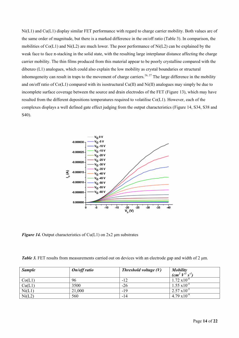
Ni(L1) and Cu(L1) display similar FET performance with regard to charge carrier mobility. Both values are of
the same order of magnitude, but there is a marked difference in the on/off ratio (Table 3). In comparison, the
mobilities of Co(L1) and Ni(L2) are much lower. The poor performance of Ni(L2) can be explained by the
weak face to face π-stacking in the solid state, with the resulting large interplanar distance affecting the charge
carrier mobility. The thin films produced from this material appear to be poorly crystalline compared with the
dibenzo (L1) analogues, which could also explain the low mobility as crystal boundaries or structural
inhomogeneity can result in traps to the movement of charge carriers.26, 27
The large difference in the mobility
and on/off ratio of Co(L1) compared with its isostructural Cu(II) and Ni(II) analogues may simply be due to
incomplete surface coverage between the source and drain electrodes of the FET (Figure 13), which may have
resulted from the different depositions temperatures required to volatilise Co(L1). However, each of the
complexes displays a well defined gate effect judging from the output characteristics (Figure 14, S34, S38 and
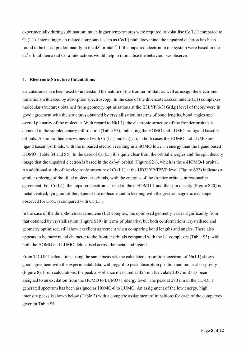
S40).
Figure 14. Output characteristics of Cu(L1) on 2x2 μm substrates
Table 3. FET results from measurements carried out on devices with an electrode gap and width of 2 μm.
Sample On/off ratio Threshold voltage (V) Mobility
(cm2 V
-1 s
-1)
Co(L1) 96 -12 1.72 x10⁻⁸
Cu(L1) 3500 -26 1.55 x10⁻⁵
Ni(L1) 21,000 -19 2.57 x10⁻⁵
Ni(L2) 560 -14 4.79 x10⁻⁹
Page 15 of 22
Magnetoresistance measurements were carried out on the Cu(L1) sample at cryogenic temperatures but the
conductivity of Co(L1) was too low to study at low temperatures. A constant gate voltage, along with a
source-drain voltage, was applied to the Cu(L1) sample as the source-drain current was measured. In the
absence of an applied gate potential the material fails to conduct a measurable source-drain current. The IV
characteristics of Cu(L1) were studied at various temperatures down to 4.35 K under a magnetic field swept
between 5 T and -5T. However, no significant magnetoresistance was witnessed. At 4.35 K a small positive
magnetoresistance (Figure S37) was observed but this was attributed to Lorentz forces from the magnetic field
scattering the charge carriers flowing perpendicular to the field, as opposed to an intrinsic material property.
Conclusions
We have prepared a series of planar Ni, Cu and Co tetraaza[14]annulene macrocyles and have carried out the
first assessment of these porphyrin analogues in thin-film devices. All the complexes exhibit p-type
semiconductivity with a gate effect in an FET configuration. Despite forming highly ordered thin films, the
hole mobilities are low. This can be rationalised by examination of the SEM images, which indicate
polycrystalline films with many grain boundaries. Accordingly, improvement of the film crystallinity is likely
to lead to much enhanced FET performance and this provides an area for future study using modified
tetraazaannulene ligands. Variation of the central metal has a marked impact on the resulting FET properties.
The key influence of the metal is in influencing the sublimation temperature and the resulting film
morphology. The different compounds necessitate slightly different deposition conditions due to their
different solid state interactions, leading to different degrees of crystallinity in the films, even for isomorphous
materials. Due to the dominant effect of the film morphology, it is difficult to directly compare the role of the
central metal between analogous complexes in terms of its electronic influence. Such a study would require
comparison of single crystal FET results or films of consistent morphology. Given however, the consistent
observation of gate-modulated transport across this series despite the non-ideal film characteristics, these
complexes provide an interesting alternative to porphyrins in the study of metal complexes for FETs, with
potential also in other electronic and optical devices. Following these initial promising results, their properties
may be further optimised through ligand modification and associated optimisation of thin-film morphology
and work in this direction is underway.
Experimental
All chemicals were purchased from Sigma Aldrich and used without further purification with the exception of
o-phenylenediamine, which was recrystallised from DCM prior to use. The complexes were synthesised from
o-phenylenediamine, 1,1,3,3-tetramethoxypropane and the corresponding metal(II) acetate salt, using an

Page 16 of 22
approach adapted from the literature.28
The resulting complexes were purified by vacuum sublimation. Single
crystals of each of the complexes were grown by vacuum sublimation, with the exception of Co(L1).Cl, which
was grown from DCM/toluene by slow evaporation.
Ni(L1). 1H NMR (CDCl3): 5.44 (t, 2H), 6.90 (m, 4H), 7.35 (m, 4H), 7.71 (d, 4H). MS (EI): m/z (%) = 344.1
(100.00%) [M+]. Calculated for C18H14NiN4, C 62.66, H 4.09, N 16.24; found C 62.55, H 3.98, N 16.13.
Cu(L1). MS (EI): m/z (%) = 349.0 (100.00%) [M+]. Calculated for C18H14CuN4, C 61.79, H 4.03, N 16.01;
found C 61.63, H 3.91, N 15.92.
Co(L1). MS (EI): m/z (%) = 345.0 (100.00%) [M+]. Calculated for C18H14CoN4, C 62.62, H 4.09, N 16.23;
found C 62.69, H 3.97, N 16.18.
Ni(L2). MS (EI): m/z (%) = 444.1 (100.00%) [M+]. Calculated for C26H18NiN4, C 70.15, H 4.08, N 12.59;
found C 69.99, H 3.99, N 12.56.
Images of the crystal structures have been produced using the software Mercury 2.3.29-32
All cyclic
voltammetry measurements were carried out in dry DCM using 0.3 M TBAPF6 electrolyte in a three electrode
system, with each solution being purged with N2 prior to measurement. The working electrode was a 0.2 mm2
Pt wire sealed in glass. The reference electrode was Ag/AgCl calibrated against Ferrocene/Ferrocenium in the
background electrolyte, and the counter electrode was a Pt rod. All measurements were made at room
temperature using an μAUTOLAB Type III potentiostat, driven by the electrochemical software GPES.
Solution UV/Vis spectra were recorded in solution in DCM using a quartz cell of path length 1 cm on a
Perkin-Elmer Lambda 9 spectrophotometer, controlled by a datalink PC, running UV/Winlab software and in
thin films on a Jasco V-570 UV/Vis/NIR spectrophotometer. Magnetic susceptibility measurements were
performed on powder samples from 1.8 to 300 K using a Quantum Design MPMS-XL SQUID magnetometer
with MPMS MultiVu Application software to process the data. The magnetic field used was 0.1 T.
Diamagnetic corrections were applied to the observed paramagnetic susceptibilities by using Pascal’s
constants. Single point and geometry optimisation calculations of the isolated complexes were carried out at
the B3LYP/6-31G(d,p) level of theory33-35
, using Gaussian 03.36
Time dependant DFT calculations were
carried out using the polarisable continuum model (PCM) for DCM which takes into account the effect of
solvation. The X-ray crystallographic coordinates were used as the starting structures. The molecular orbital
isosurfaces were visualised using ArgusLab 4.0. Thin film XRD was carried out on a Rigaku ultraX-18HB at
room temperature. Data were collected from 2θ angle of 5-40° at a rate of 2° per minute. Powder XRD was
carried out using a Bruker AXS D8 diffractometer. All the substrates for deposition, except PET and the
FETs, were cleaned in individual solutions of IPA, acetone and then chloroform prior to use. Deposition of

Page 17 of 22
Ni(L1) was carried out via vacuum sublimation in a temperature range between 335°C and 345°C at a
pressure of 5.0 x 10⁻⁴
Pa. This resulted in a growth rate of 0.2-0.4 Å/s which was monitored using a quartz
crystal microbalance (QCM). Cu(L1) was deposited between 220°C and 240°C at a pressure of 7.5 x 10⁻⁴
Pa,
which resulted in a growth rate of 0.2-0.4 Å/s. The less voltaile Co(L1) was deposited between 375°C and
385°C at a pressure of 5.2 x 10⁻⁴
Pa, which resulted in a growth rate of 0.1 Å/s. Ni(L2) was deposited between
425°C and 470°C at a pressure of 6.0 x 10⁻⁴
Pa, which resulted in a growth rate of 0.1 Å/s. The materials to be
sublimed were heated inside an inert crucible by applying a current. Films of 50 nm thickness were produced
according to the QCM. The actual thin film thickness was measured using a profileometer (Figure S2-S5).
The FET substrates used have gold source and drain electrodes with a width of 2 μm and a gap of 2 or 8 μm.
The measurements were carried out in darkness and under vacuum using a Keithley 2636A sourcemeter
equipped with Labtracer 2.0 software. Imaging of thin films was carried out using a Hitachi S-4300 Scanning
Electron Microscope.

Page 18 of 22
Notes and references
[†
]Electronic Supplementary Information (ESI) notes:
[Figure S15 Crystal structure of Co(L1)(Cl) in the presence of disordered toluene. Table S4 Crystallographic
information for Cu(L1), Ni(L2) and Co(L1)Cl.toluene. Table S5 Selected bond lengths and angles of Cu(L1)
and Ni(L2). Figure S16 Profile of Ni(L1) showing a film thickness of approximately 100 nm. Figure S17
Profile of Co(L1) showing a film thickness of approximately 90 nm. Figure S18 Profile of Cu(L1) showing a
film thickness of approximately 60 nm. Figure S19 Profile of Ni(L2) showing a film thickness of
approximately 90 nm. Figure S20 Cyclic voltammagram of Co(L1) in 0.3M TBAPF6/DCM at a scan rate of
0.1 V/s. Figure S21 Differential pulse voltammogram of Co(L1) in 0.3M TBAPF6/DCM scanning from 0 to 2
V. Figure S22 Differential pulse voltammogram of Co(L1) in 0.3M TBAPF6/DCM scanning from 0 to -2 V.
Figure S23 Cyclic voltammetry of Cu(L1) in 0.3M TBAPF6/DCM.
Figure S24 Differential pulse voltammogram of Cu(L1) in 0.3M TBAPF6/DCM. Figure S25 Cyclic
voltammetry of Ni(L1). Figure S26 The Pt working electrode before (left) and after (right) scanning 5x
between 2 and -2 V. Figure S27 Cyclic voltammetry of Ni(L1). Figure S28 Differential pulse voltammogram
of of Ni(L1) in 0.3M TBAPF6/DCM. Figure S29 Cyclic voltammagram of Ni(L2) in 0.3M TBAPF6/DCM at
a scan rate of 0.1 V/s. Figure S30 Differential pulse of Ni(L2) in 0.3M TBAPF6/DCM. Figure S31 χT vs. T
plot of Co(L1) fit to the Curie Weiss law. Figure S32 Comparison of structure obtained from geometry
optimisation calculation versus the structure obtained from single crystal diffraction. Table S6 Ni(L1) and
Ni(L2) molecular orbitals generated from DFT calculations at the B3LYP/6-31G level of theory with the
orbital energy in volts underneath. Table S7 Co(L1) orbitals and energies from single point calculations at the
B3LYP/6-31G(d,p) level of theory. Figure S33 Orbital energies of the alpha and beta orbitals of Co(L1). Also
displayed is the calculated spin density. Table S8 Cu(L1) orbitals and energies from single point calculations
at the B3LYP/6-31G(d,p) level of theory. Figure S34 Comparison of structure obtained from geometry
optimisation calculation versus the structure obtained from single crystal diffraction. Table S9 Ni(L1) and
Ni(L2) molecular orbitals generated from DFT calculations at the B3LYP/6-31G level of theory with the
orbital energy in volts underneath. Table S10 Co(L1) orbitals and energies from single point calculations at
the B3LYP/6-31G(d,p) level of theory. Figure S35 Orbital energies of the alpha and beta orbitals of Co(L1).
Also displayed is the calculated spin density.
Table S11 Cu(L1) orbitals and energies from single point calculations at the B3LYP/6-31G(d,p) level of
theory. Figure S36 Cu(L1) calculation at the B3LYP/6-31G(d,p) level of theory showing the energies of the
frontier orbitals and the spin density. Figure S37 Cu(L1) calculation at the UB3LYP/TZVP level of theory
showing the energies of the frontier orbitals and the spin density. Figure S38 TD-DFT generated absorption
spectra overlaid with an experimental solution measurement of Cu(L1).

Page 19 of 22
Figure S39 TD-DFT generated absorption spectra overlaid with an experimental solution measurement of
Co(L1). Figure S40 TD-DFT generated absorption spectra overlaid with an experimental solution
measurement of Ni(L2). Table S12 TD-DFT assignment of electronic absorption spectra between 250 and
1000 nm. Figure S41 Thin film diffraction pattern of Co(L1) in black, overlaid with the powder pattern in red.
Figure S42 Thin film diffraction pattern of Cu(L1) in black, overlaid with the powder pattern in red and
single crystal generated pattern in blue.
Figure S43 Unit cell of Ni(L1) with the (200) plane highlighted in red. Figure S44 Possible reflections from
Ni(L2) thin film XRD. Figure S45 Thin film absorption of Cu(L1) with solution spectrum overlaid. Figure
S46 Thin film absorption of Co(L1) with solution spectrum overlaid. Figure S47 Thin film absorption of
Ni(L1) with solution spectrum overlaid. Figure S48 SEM image of Ni(L2). Figure S49 Output characteristics
of Ni(L1) on 2x2 μm substrates. Figure S50 Transfer characteristics of Ni(L1) on 2x2 μm substrates. Figure
S51 Transfer characteristics of Cu(L1) on 2x2 μm substrates. Figure S52 Magnetoresistance measurement on
Cu(L1) at 4.35 K when applying a gate voltage of -60 V and a drain voltage of -40 V. Figure S53 Output
characteristics of Co(L1) on 2x2 μm substrates. Figure S54 Transfer characteristics of Co(L1) on 2x2 μm
substrates. Figure S55 Output characteristics of Ni(L2) on 2x2 μm substrates. Figure S56 Transfer
characteristics of Ni(L2) on 2x2 μm substrates.]. See DOI: 10.1039/b000000x/
[1] Y. Zhang, X. Cai, Y. Bian and J. Jiang, Springer Berlin / Heidelberg, 2010, pp. 275-321.
[2] F. Garnier, X. Peng, G. Horowitz and D. Fichou, Molecular Engineering, 1991, 1, 131-139.
[3] Z. Bao, A. J. Lovinger and A. Dodabalapur, Applied Physics Letters, 1996, 69, 3066-3068.
[4] P. Ma, Y. Chen, X. Cai, H. Wang, Y. Zhang, Y. Gao and J. Jiang, Synthetic Metals, 2010, 160, 510-515.
[5] D. Hohnholz, S. Steinbrecher and M. Hanack, Journal of Molecular Structure, 2000, 521, 231-237.
[6] H.-S. Kim and C. C. Wamser, Photochemical & Photobiological Sciences, 2006, 5, 955-960.
[7] M. V. Martinez-Diaz, G. de la Torre and T. Torres, Chemical Communications, 2010, 46, 7090-7108.
[8] T. Minari, Appl. Phys. Lett., 2007, 91, 123501.
[9] M. H. Hoang, Y. Kim, S.-J. Kim, D. H. Choi and S. J. Lee, Chemistry – A European Journal, 2011, 17,
7772-7776.
[10] N. B. Chaure and et al., Science and Technology of Advanced Materials, 12, 025001.
[11] Liqiang Li, Qingxin Tang, Hongxiang Li, Wenping Hu, Xiaodi Yang, Zhigang Shuai, Yunqi Liu and D.
Zhu, Pure Appl. Chem., 2008, 80, 2231–2240.

Page 20 of 22
[12] V. Plyashkevich, T. Basova, I. Yushina and I. Igumenov, Journal of Surface Investigation: X-ray,
Synchrotron and Neutron Techniques, 2008, 2, 423-428.
[13] T. Basova, E. Kol'tsov, A. Hassan, A. Tsargorodskaya, A. Ray and I. Igumenov, physica status solidi (b),
2005, 242, 822-827.
[14] J. Puigdollers, C. Voz, M. Fonrodona, S. Cheylan, M. Stella, J. Andreu, M. Vetter and R. Alcubilla,
Journal of Non-Crystalline Solids, 2006, 352, 1778-1782.
[15] P. Mountford, Chemical Society Reviews, 1998, 27, 105-116.
[16] L. G. Bell and J. C. Dabrowiak, Journal of the Chemical Society, Chemical Communications, 1975, 512-
513.
[17] P. J. Lukes, J. A. Crayston, D. J. Ando, M. E. Harman and M. B. Hursthouse, Journal of the Chemical
Society, Perkin Transactions 2, 1991, 1845-1849.
[18] L.-S. Lin, T. J. Marks, C. R. Kannewurf, J. W. Lyding, M. S. McClure, M. T. Ratajack and T.-C. Whang,
Journal of the Chemical Society, Chemical Communications, 1980, 954-955.
[19] M. C. Weiss, G. Gordon and V. L. Goedken, Inorganic Chemistry, 1977, 16, 305-310.
[20] P. J. Lukes, A. C. McGregor, T. Clifford and J. A. Crayston, Inorganic Chemistry, 1992, 31, 4697-4699.
[21] P. J. Hochgesang and R. D. Bereman, Inorganica Chimica Acta, 1988, 149, 69-76.
[22] C. Miry, D. Le Brun, J.-M. Kerbaol and M. L'Her, Journal of Electroanalytical Chemistry, 2000, 494,
53-59.
[23] F. C. McElroy and J. C. Dabrowiak, Journal of the American Chemical Society, 1976, 98, 7112-7113.
[24] W. E. Estes, D. P. Gavel, W. E. Hatfield and D. J. Hodgson, Inorganic Chemistry, 1978, 17, 1415-1421.
[25] J. M. Assour and W. K. Kahn, Journal of the American Chemical Society, 1965, 87, 207-212.
[26] L. G. Kaake, P. F. Barbara and X. Y. Zhu, The Journal of Physical Chemistry Letters, 2010, 1, 628-635.
[27] M. Tello, M. Chiesa, C. M. Duffy and H. Sirringhaus, Advanced Functional Materials, 2008, 18, 3907-
3913.
[28] A. R. Cutler, C. S. Alleyne and D. Dolphin, Inorganic Chemistry, 1985, 24, 2276-2281.
[29] R. Taylor and C. F. Macrae, Acta Crystallographica Section B, 2001, 57, 815-827.

Page 21 of 22
[30] I. J. Bruno, J. C. Cole, P. R. Edgington, M. Kessler, C. F. Macrae, P. McCabe, J. Pearson and R. Taylor,
Acta Crystallographica Section B, 2002, 58, 389-397.
[31] C. F. Macrae, I. J. Bruno, J. A. Chisholm, P. R. Edgington, P. McCabe, E. Pidcock, L. Rodriguez-Monge,
R. Taylor, J. van de Streek and P. A. Wood, Journal of Applied Crystallography, 2008, 41, 466-470.
[32] C. F. Macrae, P. R. Edgington, P. McCabe, E. Pidcock, G. P. Shields, R. Taylor, M. Towler and J. van de
Streek, Journal of Applied Crystallography, 2006, 39, 453-457.
[33] A. D. Becke, J. Chem. Phys., 1993, 98, 5648-5652.
[34] C. Lee, W. Yang and R. G. Parr, Phys. Rev. B, 1988, 37, 785-789.
[35] R. Ditchfield, W. J. Hehre and J. A. Pople, The Journal of Chemical Physics, 1971, 54, 724-728.
[36] M. J. Frisch, G. W. Trucks, H. B. Schlegel, G. E. Scuseria, M. A. Robb, J. R. Cheeseman, J. J. A.
Montgomery, T. Vreven, K. N. Kudin, J. C. Burant, J. M. Millam, S. S. Iyengar, J. Tomasi, V. Barone, B.
Mennucci, M. Cossi, G. Scalmani, N. Rega, G. A. Petersson, H. Nakatsuji, M. Hada, M. Ehara, K.
Toyota, R. Fukuda, J. Hasegawa, M. Ishida, T. Nakajima, Y. Honda, O. Kitao, H. Nakai, M. Klene, X. Li,
J. E. Knox, H. P. Hratchian, J. B. Cross, V. Bakken, C. Adamo, J. Jaramillo, R. Gomperts, R. E.
Stratmann, O. Yazyev, A. J. Austin, R. Cammi, C. Pomelli, J. W. Ochterski, P. Y. Ayala, K. Morokuma,
G. A. Voth, P. Salvador, J. J. Dannenberg, V. G. Zakrzewski, S. Dapprich, A. D. Daniels, M. C. Strain, O.
Farkas, D. K. Malick, A. D. Rabuck, K. Raghavachari, J. B. Foresman, J. V. Ortiz, Q. Cui, A. G. Baboul,
S. Clifford, J. Cioslowski, B. B. Stefanov, G. Liu, A. Liashenko, P. Piskorz, I. Komaromi, R. L. Martin,
D. J. Fox, T. Keith, M. A. Al-Laham, C. Y. Peng, A. Nanayakkara, M. Challacombe, P. M. W. Gill, B.
Johnson, W. Chen, M. W. Wong, C. Gonzalez and J. A. Pople, ed. Gaussian, Wallingford CT, 2004.