
ECFA LEVEL-1 MOS TRANSISTOR MODEL
43
Transcript of ECFA LEVEL-1 MOS TRANSISTOR MODEL
References
• B. Razavi, ”Design of Analog CMOS Integrated Circuits”, Mc Graw-Hill, 2001.
• K. Martin & D. Johns, “Analog Integrated Circuits Design”, John Wiley, 1997.
• W. Sansen & K. Laker, “Design of Analog Integrated Circuits & Systems”, Mc Graw-Hill, 1994.
• P. Gray & R. Meyer, “Analysis and Design of Analog Integrated Circuits”, third edition, John Wiley 1993.
• G. Temes & R. Gregorian, “Analog MOS Integrated Circuits for Signal Processing”, John Wiley, 1986.
• Jacky Porte,”OCEANE: Outils pour la Conception et l' Enseignement des circuits intégrés ANalogiquEs”, http://www-asim.lip6.fr/recherche/analog/oceane/
H. Aboushady University of Paris VI
Lecture I Basic MOS Device Physics
H. Aboushady University of Paris VI
���Basic MOS Device Physics
• The MOSFET structure
• MOS I/V Characteristics
• Second Order Effects
• MOS Device models
H. Aboushady University of Paris VI
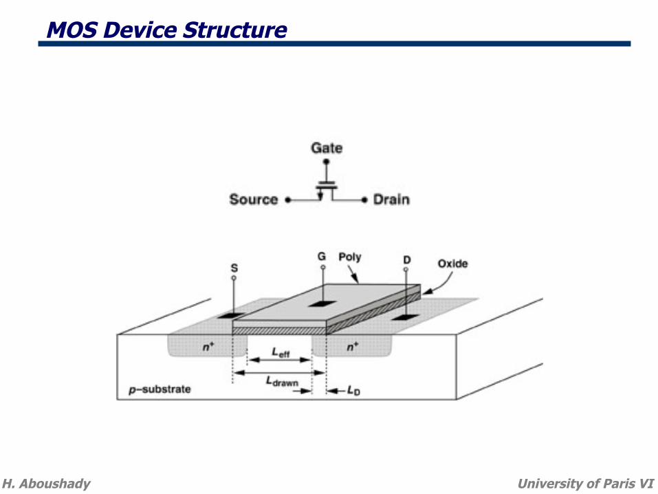
MOS Device Structure
H. Aboushady University of Paris VI
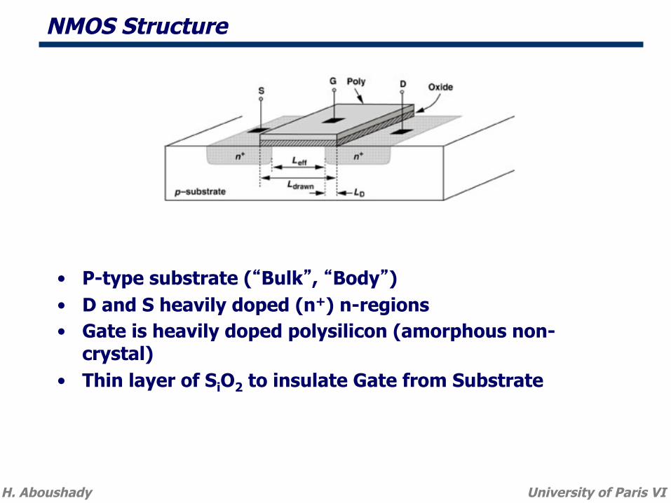
NMOS Structure
• P-type substrate (“Bulk”, “Body”) • D and S heavily doped (n+) n-regions • Gate is heavily doped polysilicon (amorphous non-
crystal) • Thin layer of SiO2 to insulate Gate from Substrate
H. Aboushady University of Paris VI
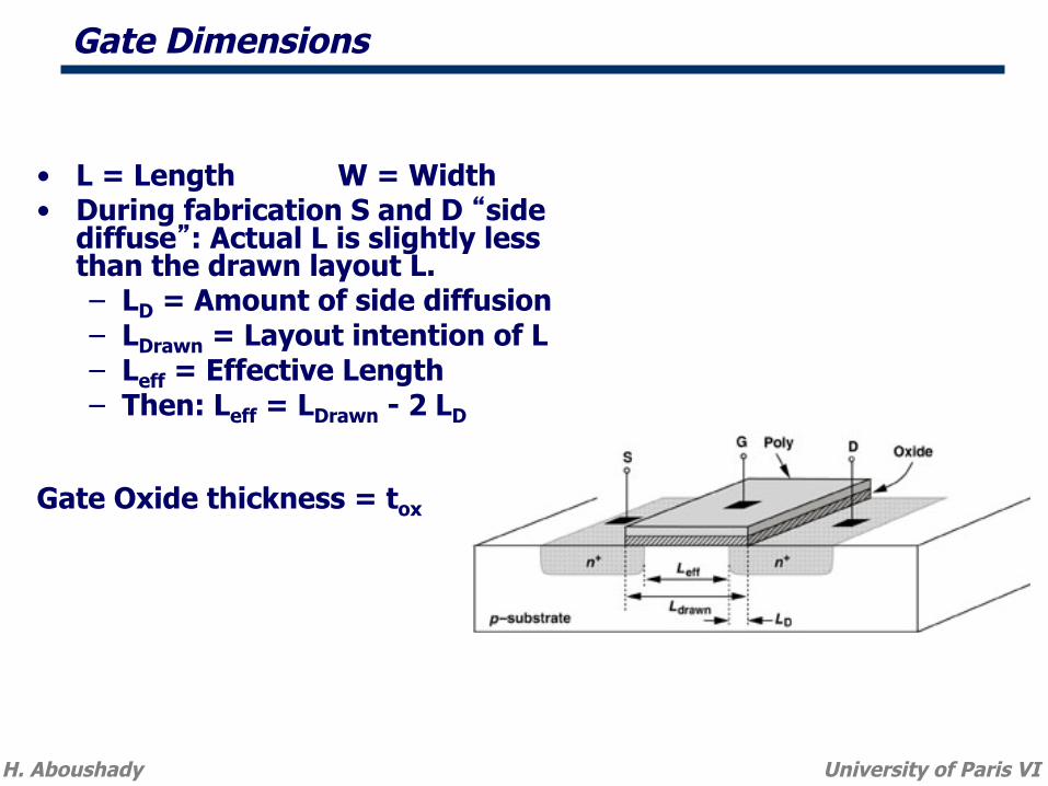
Gate Dimensions
• L = Length W = Width • During fabrication S and D “side
diffuse”: Actual L is slightly less than the drawn layout L. – LD = Amount of side diffusion – LDrawn = Layout intention of L – Leff = Effective Length – Then: Leff = LDrawn - 2 LD
Gate Oxide thickness = tox
H. Aboushady University of Paris VI
Technology Trends
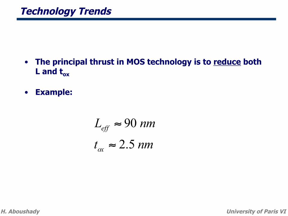
• The principal thrust in MOS technology is to reduce both L and tox
• Example:
nmtnmL
ox
eff
5.2
90
≈
≈
H. Aboushady University of Paris VI
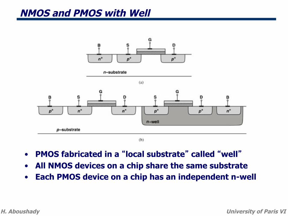
NMOS and PMOS with Well
• PMOS fabricated in a “local substrate” called “well” • All NMOS devices on a chip share the same substrate • Each PMOS device on a chip has an independent n-well
H. Aboushady University of Paris VI
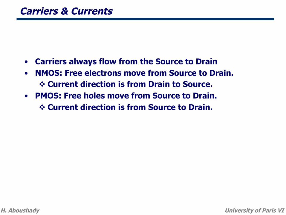
• Carriers always flow from the Source to Drain • NMOS: Free electrons move from Source to Drain.
! Current direction is from Drain to Source. • PMOS: Free holes move from Source to Drain.
! Current direction is from Source to Drain.
Carriers & Currents
H. Aboushady University of Paris VI
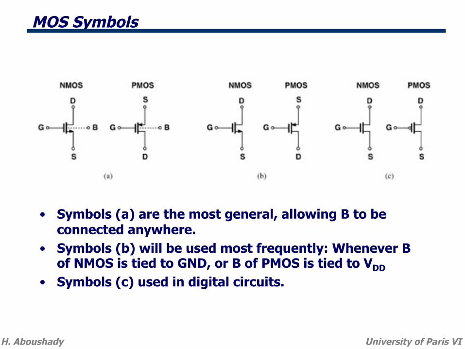
• Symbols (a) are the most general, allowing B to be connected anywhere.
• Symbols (b) will be used most frequently: Whenever B of NMOS is tied to GND, or B of PMOS is tied to VDD
• Symbols (c) used in digital circuits.
MOS Symbols
H. Aboushady University of Paris VI
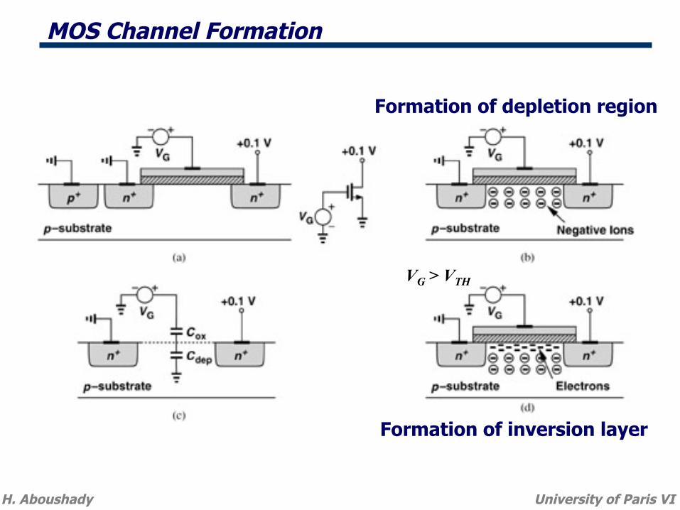
MOS Channel Formation
Formation of inversion layer
Formation of depletion region
VG > VTH
H. Aboushady University of Paris VI
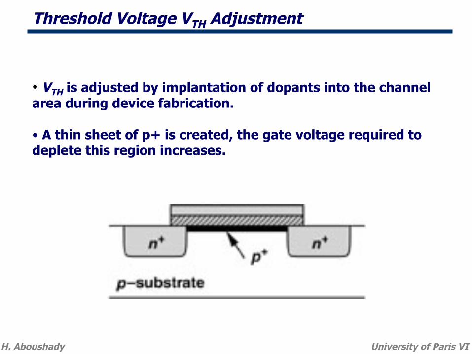
Threshold Voltage VTH Adjustment
• VTH is adjusted by implantation of dopants into the channel area during device fabrication.
• A thin sheet of p+ is created, the gate voltage required to deplete this region increases.
H. Aboushady University of Paris VI
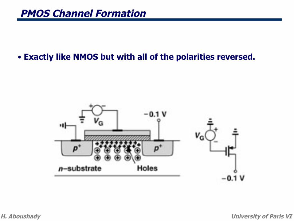
PMOS Channel Formation
• Exactly like NMOS but with all of the polarities reversed.
H. Aboushady University of Paris VI
���Basic MOS Device Physics
• The MOSFET structure
• MOS I/V Characteristics
• Second Order Effects
• MOS Device models
H. Aboushady University of Paris VI
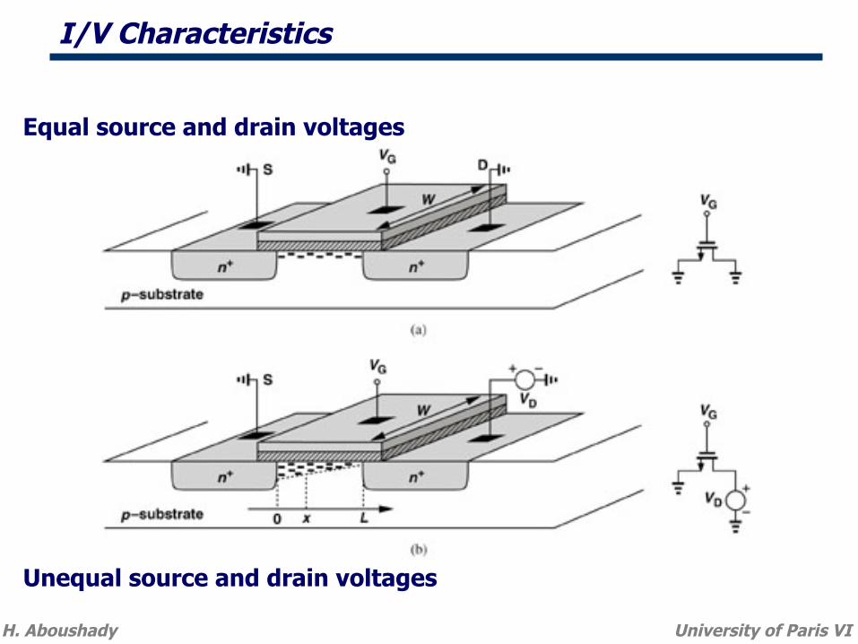
I/V Characteristics
H. Aboushady University of Paris VI
Equal source and drain voltages
Unequal source and drain voltages
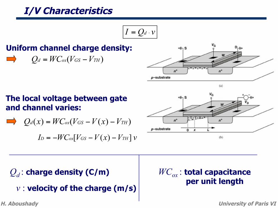
I/V Characteristics
)( THGSoxd VVWCQ −=
vQI d ⋅=
WCox : total capacitance per unit length
H. Aboushady University of Paris VI
))(()( THGSoxd VxVVWCxQ −−=
vVxVVWCI THGSoxD ])([ −−−=
Uniform channel charge density:
The local voltage between gate and channel varies:
v : velocity of the charge (m/s)
Qd : charge density (C/m)
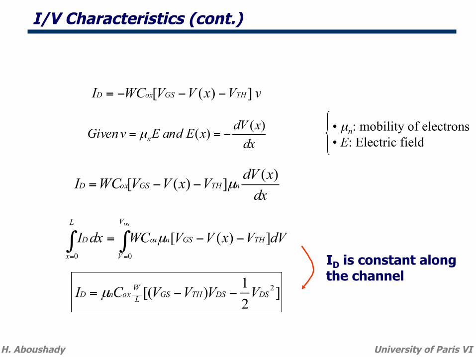
I/V Characteristics (cont.)
vVxVVWCI THGSoxD ])([ −−−=
∫∫==
−−=DSV
V
THGSnox
L
x
D dVVxVVWCdxI00
])([µ
dxxdVxEandEvGiven n)()( −== µ
dxxdVVxVVWCI nTHGSoxD)(])([ µ−−=
]21)[( 2
DSDSTHGSLW
oxnD VVVVCI −−= µ
• µn: mobility of electrons • E: Electric field
H. Aboushady University of Paris VI
ID is constant along the channel
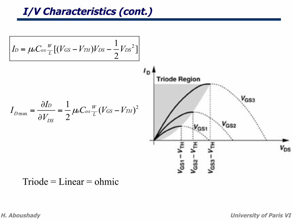
I/V Characteristics (cont.)
]21)[( 2
DSDSTHGSLW
oxnD VVVVCI −−= µ
Triode = Linear = ohmic
H. Aboushady University of Paris VI
2max )(
21
THGSLW
oxn
DS
DD VVC
VII −=
∂
∂= µ
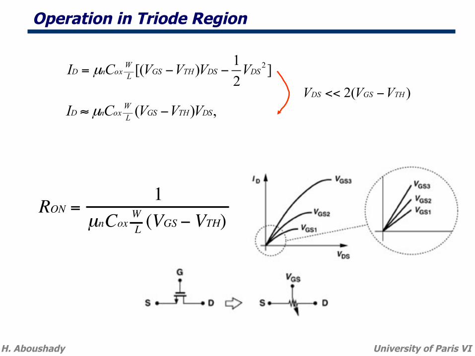
Operation in Triode Region
]21)[( 2
DSDSTHGSLW
oxnD VVVVCI −−= µ
,)( DSTHGSLW
oxnD VVVCI −≈ µ
RON =1
µnCoxWL (VGS − VTH)
H. Aboushady University of Paris VI
)(2 THGSDS VVV −<<
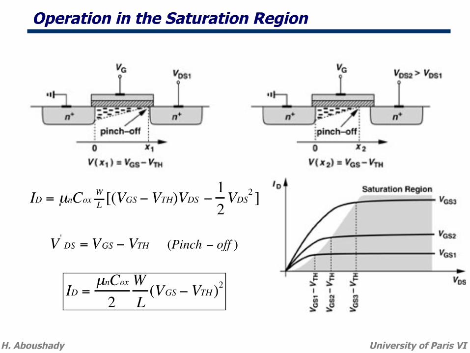
Operation in the Saturation Region
ID = µnCoxWL [(VGS − VTH)VDS −
12VDS
2 ]
ID =µnCox
2WL(VGS − VTH)2
V 'DS = VGS − VTH (Pinch − off )
H. Aboushady University of Paris VI

Saturated MOS Operating as a Current Source
H. Aboushady University of Paris VI
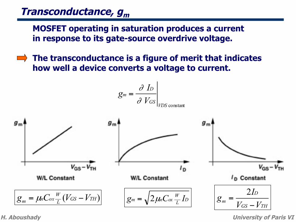
Transconductance, gm
constant VDSGS
Dm
VIg
∂∂
=
)( THGSLW
oxnm VVCg −= µ DLW
oxnm ICg µ2=THGS
Dm VV
Ig−
=2
H. Aboushady University of Paris VI
MOSFET operating in saturation produces a current in response to its gate-source overdrive voltage. The transconductance is a figure of merit that indicates how well a device converts a voltage to current.
���Basic MOS Device Physics
• The MOSFET structure
• MOS I/V Characteristics
• Second Order Effects
• MOS Device models
H. Aboushady University of Paris VI
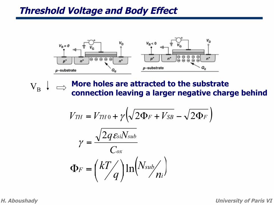
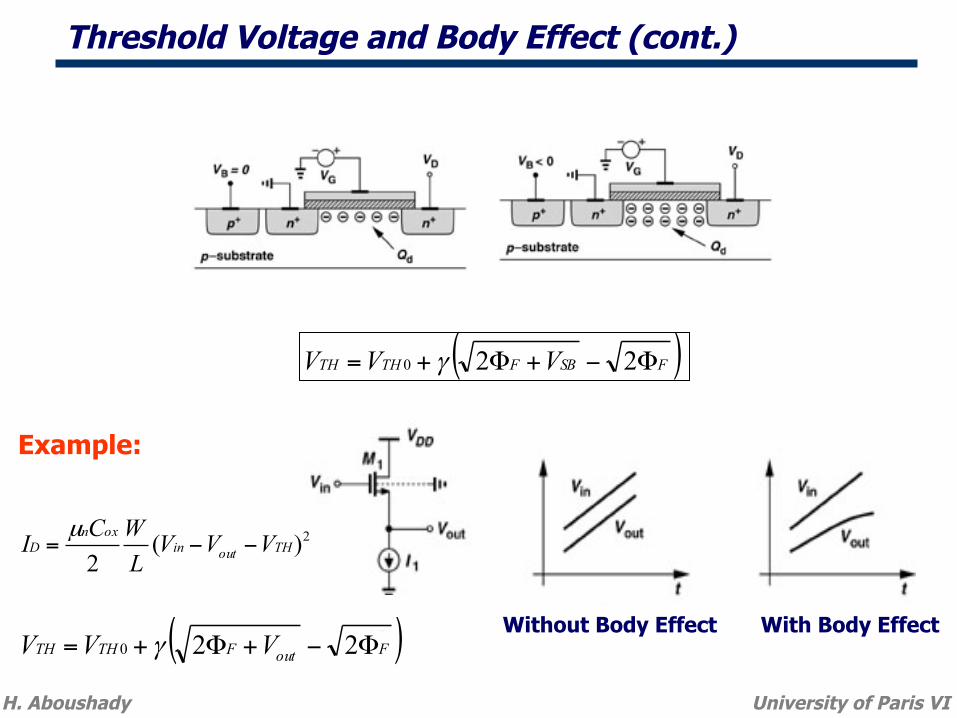
Threshold Voltage and Body Effect
VB More holes are attracted to the substrate connection leaving a larger negative charge behind
( ) 220 FSBFTHTH VVV Φ−+Φ+= γ
( )i
subF nN
qkT ln⎟
⎠⎞⎜
⎝⎛=Φ
ox
subsi
CNqε
γ2
=
H. Aboushady University of Paris VI
Threshold Voltage and Body Effect (cont.)
Nsub= doping concentrationof the substrate ni = intrinsic carrier concentration in silicon q = electron charge ΦF = Fermi-level Cox = gate oxide capacitance per unit area εsi = silicon dielectric constant
H. Aboushady University of Paris VI
Threshold Voltage and Body Effect (cont.)
( ) 220 FSBFTHTH VVV Φ−+Φ+= γ
H. Aboushady University of Paris VI
Without Body Effect With Body Effect
2)(2
THoutinoxn
D VVVLWCI −−=
µ
Example:
( ) 220 FoutFTHTH VVV Φ−+Φ+= γ
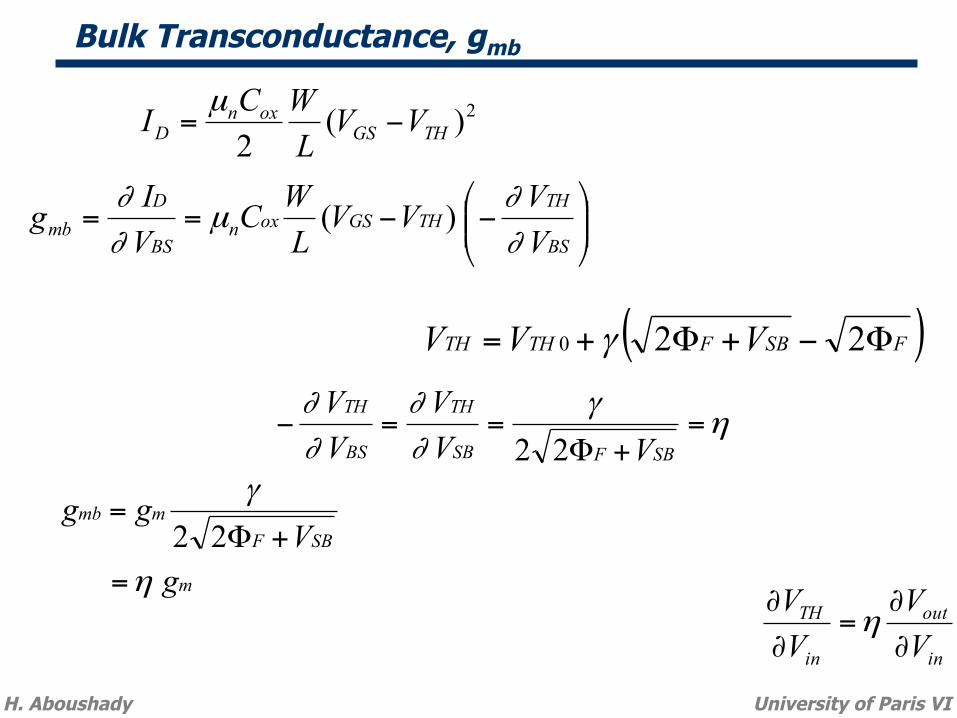
Bulk Transconductance, gmb
H. Aboushady University of Paris VI
in
out
in
TH
VV
VV
∂
∂=
∂
∂η
⎟⎟⎠
⎞⎜⎜⎝
⎛−−==
BS
THTHGSoxn
BS
Dmb V
VVVLWC
VIg
∂∂
µ∂∂ )(
m
SBFmmb
gV
gg
η
γ
=+Φ
=22
ηγ
∂∂
∂∂
=+Φ
==−SBFSB
TH
BS
TH
VVV
VV
22
2)(2 THGSoxn
D VVLWCI −=
µ
( ) 220 FSBFTHTH VVV Φ−+Φ+= γ
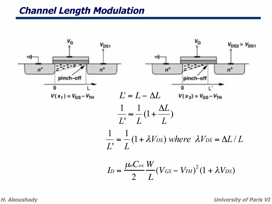
Channel Length Modulation
L' = L − ΔL
)1(1'1
LL
LLΔ
+≈
LLVwhereVLL
DSDS / )1(1'
1Δ=+= λλ
ID =µnCox
2WL(VGS − VTH)2 (1 + λVDS)
L L’
H. Aboushady University of Paris VI
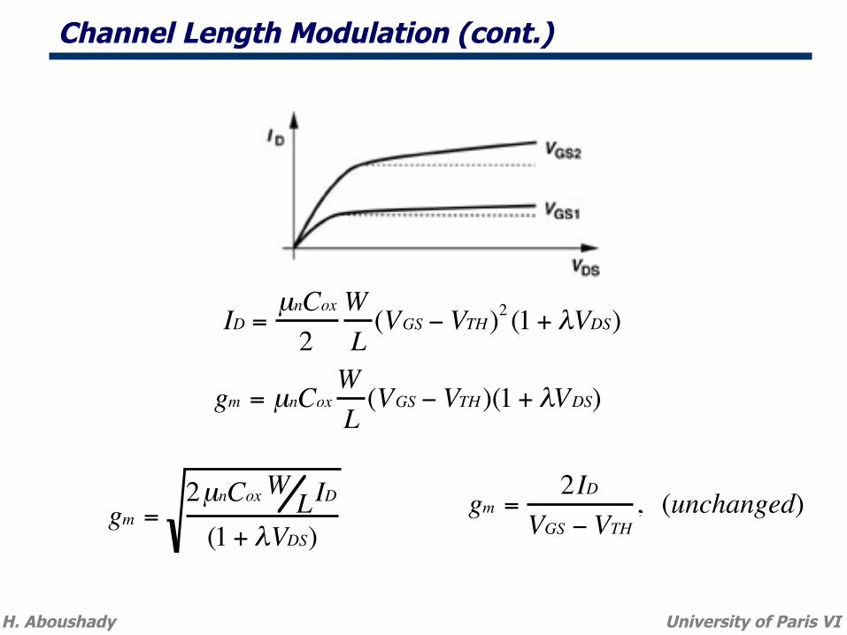
Channel Length Modulation (cont.)
gm = µnCoxWL(VGS − VTH)(1 + λVDS)
gm =2µnCoxW LID(1 + λVDS)
gm =2ID
VGS − VTH, (unchanged)
ID =µnCox
2WL(VGS − VTH)2 (1 + λVDS)
H. Aboushady University of Paris VI
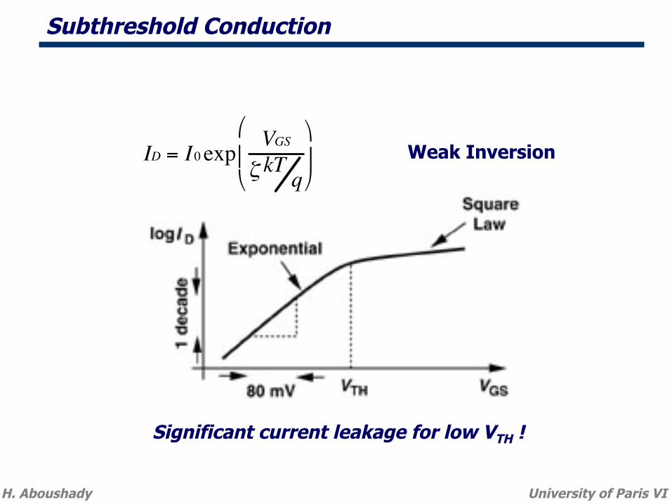
Subthreshold Conduction
ID = I0 exp VGSζ kT q
"
# $
%
& ' Weak Inversion
Significant current leakage for low VTH !
H. Aboushady University of Paris VI
���Basic MOS Device Physics
• The MOSFET structure
• MOS I/V Characteristics
• Second Order Effects
• MOS Device models
H. Aboushady University of Paris VI
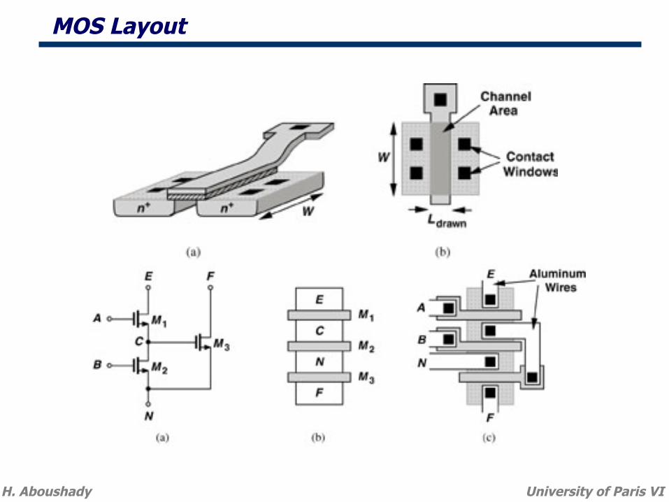
MOS Layout
H. Aboushady University of Paris VI
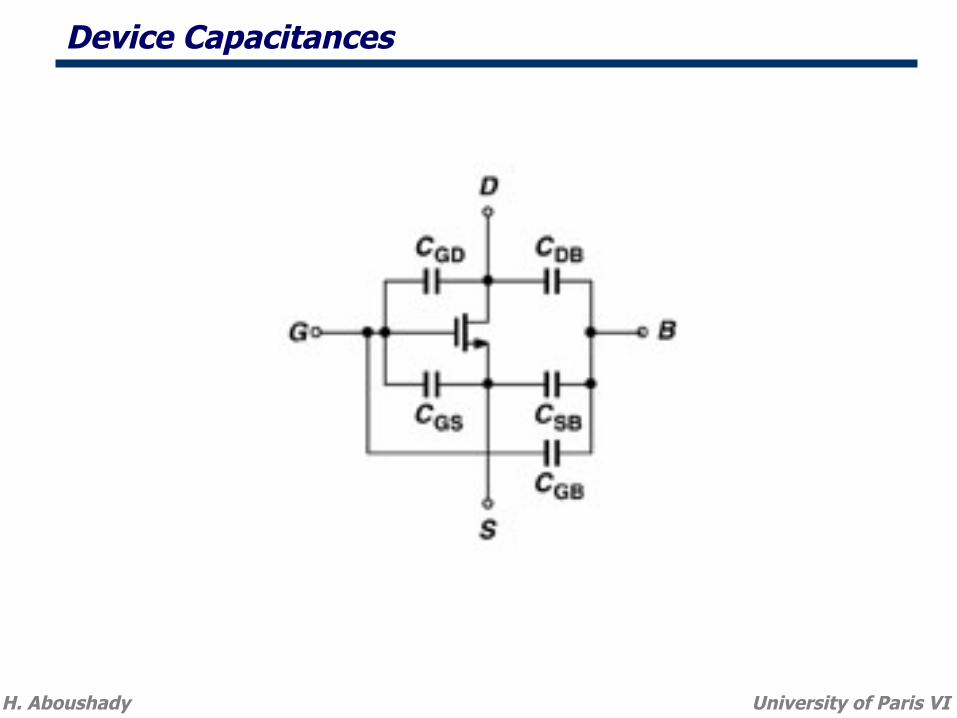
Device Capacitances
H. Aboushady University of Paris VI
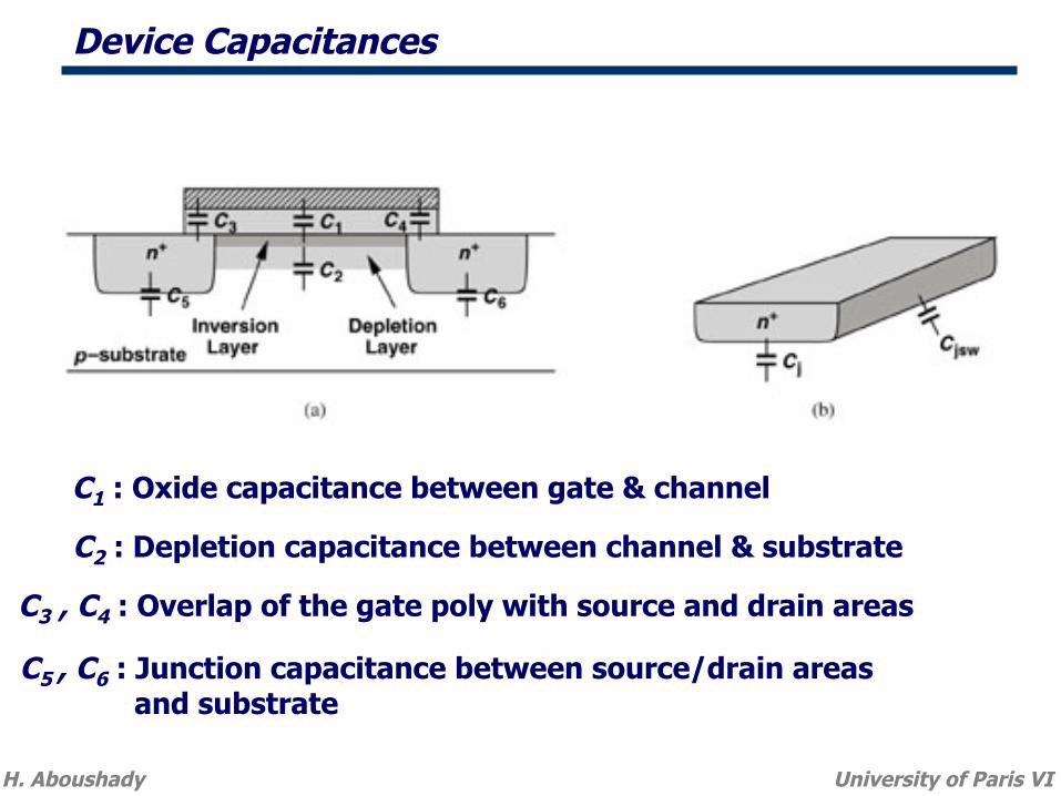
Device Capacitances
C1 : Oxide capacitance between gate & channel
C2 : Depletion capacitance between channel & substrate
C3 , C4 : Overlap of the gate poly with source and drain areas
C5 , C6 : Junction capacitance between source/drain areas and substrate
H. Aboushady University of Paris VI
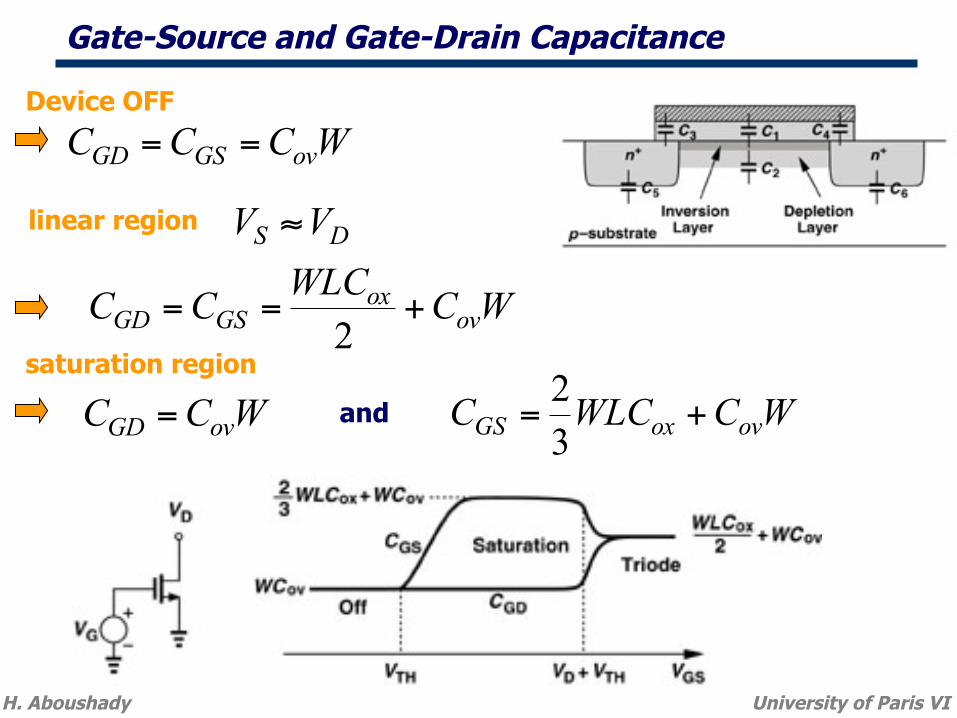
Gate-Source and Gate-Drain Capacitance
H. Aboushady University of Paris VI
linear region
WCWLCCC ovox
GSGD +==2
DS VV ≈
saturation region
WCC ovGD = WCWLCC ovoxGS +=32
WCCC ovGSGD ==Device OFF
and
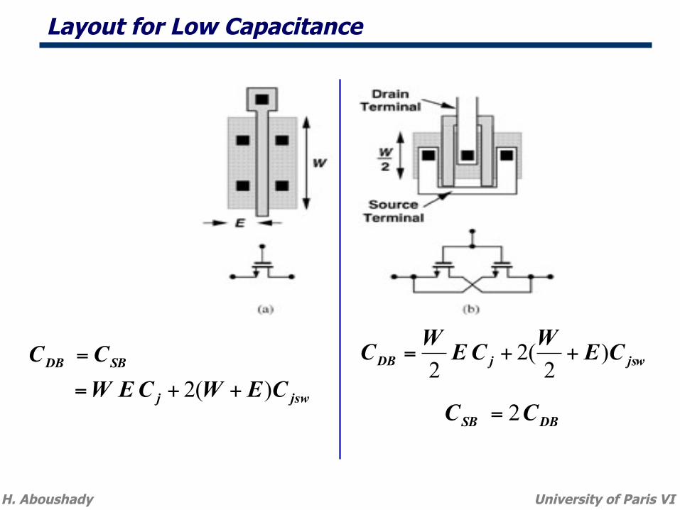
Layout for Low Capacitance
jswj
SBDB
CEWCEWCC
)(2 ++=
= jswjDB CEWCEWC )2(2
2++=
DBSB CC 2=
H. Aboushady University of Paris VI
MOS Small Signal Model
H. Aboushady University of Paris VI
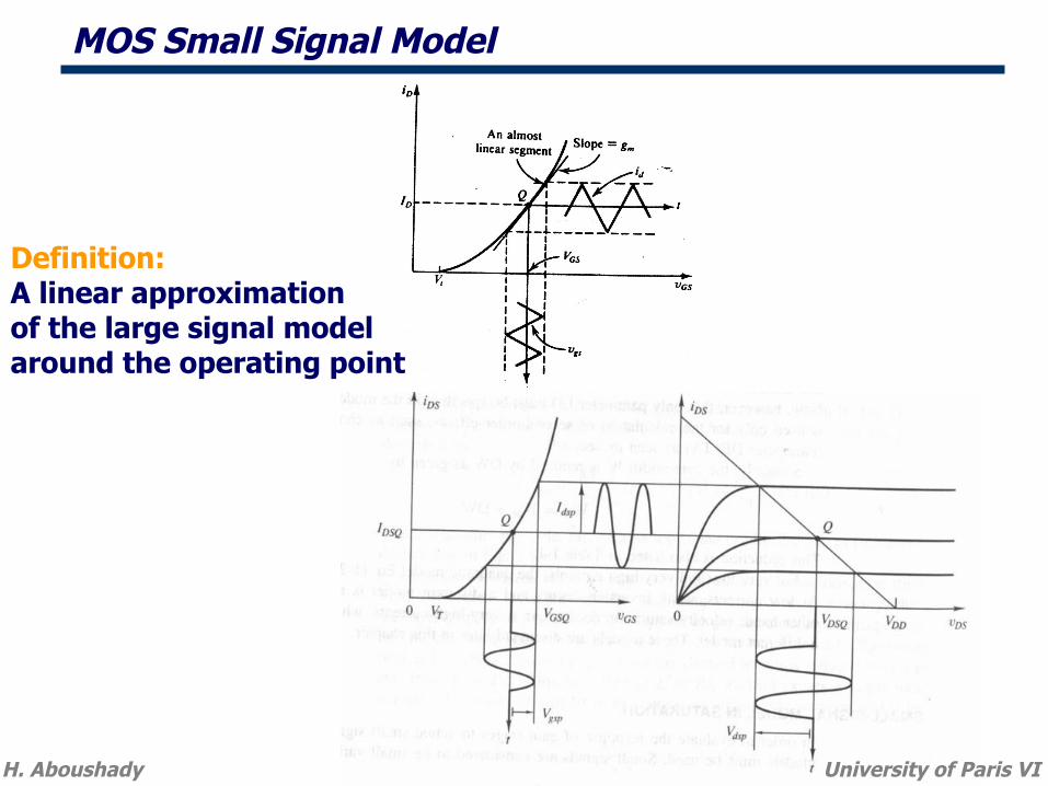
Definition: A linear approximation of the large signal model around the operating point
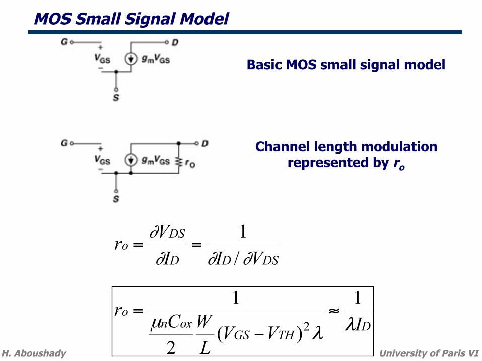
MOS Small Signal Model
Basic MOS small signal model
Channel length modulation represented by ro
H. Aboushady University of Paris VI
DTHGS
oxno
IVVLWCr
λλµ
1
)(2
12
≈−
=
DSDD
DSo
VIIVr
∂∂∂∂
/1
==
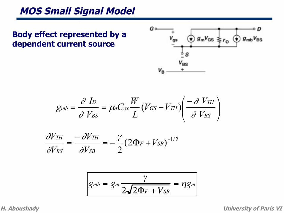
Body effect represented by a dependent current source
⎟⎟⎠
⎞⎜⎜⎝
⎛ −−==
BS
THTHGSoxn
BS
Dmb
VVVV
LWC
VIg
∂∂
µ∂∂ )(
gmb = gm γ2 2ΦF +VSB
= ηgm
2/1)2(2
−+Φ−=−
= SBFSB
TH
BS
TH VVV
VV γ
∂∂
∂∂
H. Aboushady University of Paris VI
MOS Small Signal Model
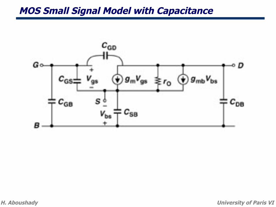
MOS Small Signal Model with Capacitance
H. Aboushady University of Paris VI
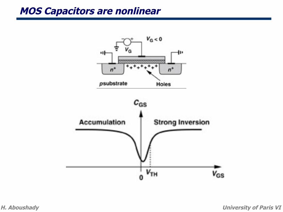
MOS Capacitors are nonlinear
H. Aboushady University of Paris VI
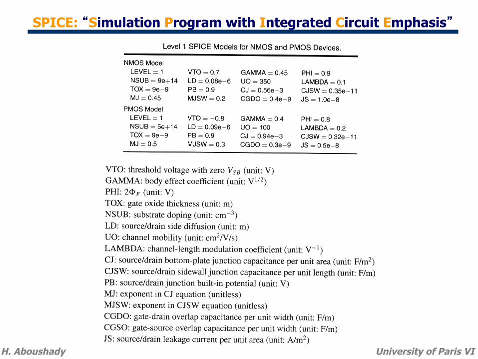
SPICE: “Simulation Program with Integrated Circuit Emphasis”
H. Aboushady University of Paris VI