MOS Transistor Theoryjmorizio/ece261/classlectures/MOS_theory.pdf · MOS Transistor Theory • So...
65
EE 261 James Morizio 1 MOS Transistor Theory • So far, we have viewed a MOS transistor as an ideal switch (digital operation) – Reality: less than ideal
Transcript of MOS Transistor Theoryjmorizio/ece261/classlectures/MOS_theory.pdf · MOS Transistor Theory • So...
EE 261 James Morizio 1
MOS Transistor Theory
• So far, we have viewed a MOS transistor as an ideal switch (digital operation)– Reality: less than ideal

EE 261 James Morizio 2
EE 261 James Morizio 3
Introduction• So far, we have treated transistors as ideal
switches• An ON transistor passes a finite amount of current
– Depends on terminal voltages– Derive current-voltage (I-V) relationships
• Transistor gate, source, drain all have capacitance– I = C (∆V/∆t) -> ∆t = (C/I) ∆V– Capacitance and current determine speed
• Also explore what a “degraded level” really means
EE 261 James Morizio 4
MOS Transistor Theory
• Study conducting channel between source and drain• Modulated by voltage applied to the gate (voltage-controlled device)• nMOS transistor: majority carriers are electrons (greater mobility), p-substrate doped (positively doped)• pMOS transistor: majority carriers are holes (less mobility), n-substrate (negatively doped)
EE 261 James Morizio 5
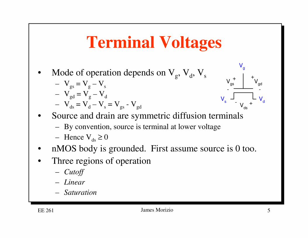
Terminal Voltages• Mode of operation depends on Vg, Vd, Vs
– Vgs = Vg – Vs
– Vgd = Vg – Vd
– Vds = Vd – Vs = Vgs - Vgd
• Source and drain are symmetric diffusion terminals– By convention, source is terminal at lower voltage– Hence Vds ≥ 0
• nMOS body is grounded. First assume source is 0 too.• Three regions of operation
– Cutoff– Linear– Saturation
Vg
Vs Vd
VgdVgs
Vds+-
+
-
+
-

EE 261 James Morizio 6
Gate Biasing
p-substrate
n+ n+
Source Gate Drain
Channel
+ -
E
SiO2
VSS (Gnd)
• Vgs=0: no current flows fromsource to drain (insulated by two reverse biased pn junctions
• Vgs>0: electric field created across substrate
• Electrons accumulate under gate: region changes from p-typeto n-type
• Conduction path between source and drain
EE 261 James Morizio 7
nMOS Device Behavior
Vgs << Vt
Polysilicon gatep-substrate
Accumulationmode
• Enhancement-mode transistor: Conducts when gate biasVgs > Vt
• Depletion-mode transistor: Conducts when gate bias is zero
Vgs = Vt
Depletion mode
Depletion region
Oxide insulator
Vgs > Vt
Inversion mode
Depletion region
InversionRegion(n-type)
EE 261 James Morizio 8
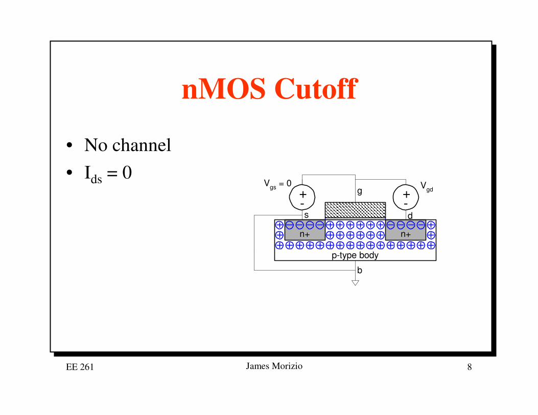
nMOS Cutoff
• No channel• Ids = 0
+-
Vgs = 0
n+ n+
+-
Vgd
p-type body
b
g
s d
EE 261 James Morizio 9
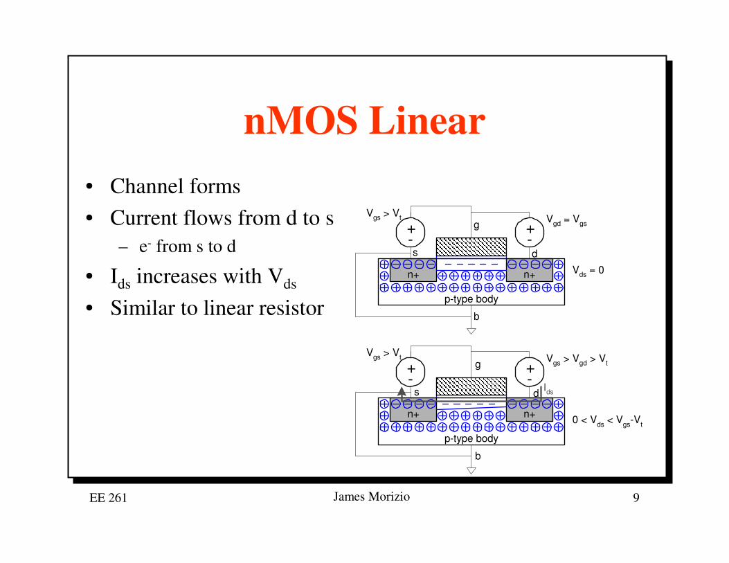
nMOS Linear• Channel forms• Current flows from d to s
– e- from s to d
• Ids increases with Vds
• Similar to linear resistor
+-
Vgs > Vt
n+ n+
+-
Vgd = Vgs
+-
Vgs > Vt
n+ n+
+-
Vgs > Vgd > Vt
Vds = 0
0 < Vds < Vgs-Vt
p-type body
p-type body
b
g
s d
b
g
s d Ids
EE 261 James Morizio 10
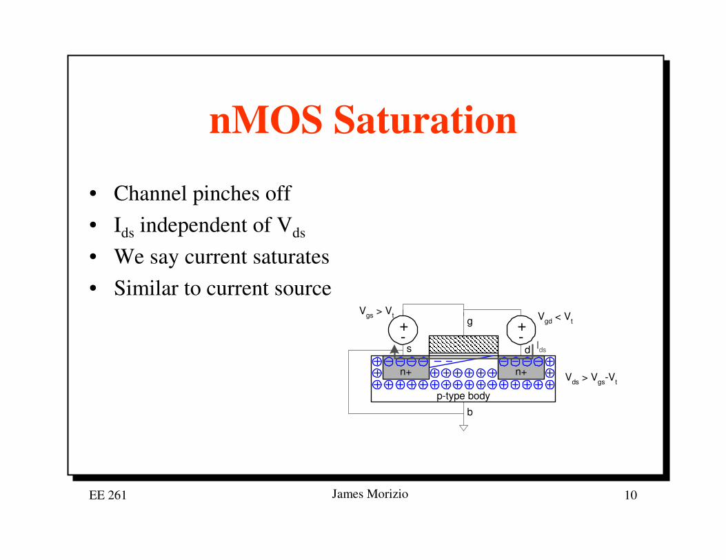
nMOS Saturation
• Channel pinches off• Ids independent of Vds
• We say current saturates• Similar to current source
+-
Vgs > Vt
n+ n+
+-
Vgd < Vt
Vds > Vgs-Vt
p-type body
b
g
s d Ids
EE 261 James Morizio 11
I-V Characteristics
• In linear region, Ids depends on– How much charge is in the channel?– How fast is the charge moving?
EE 261 James Morizio 12
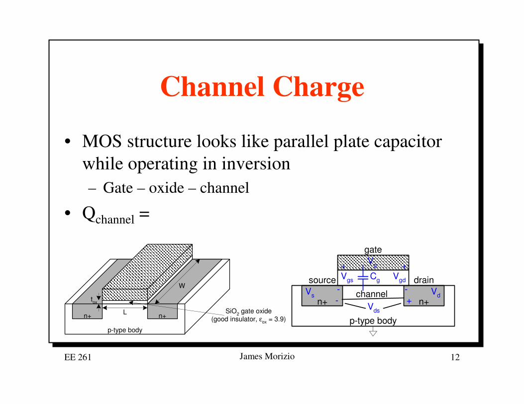
Channel Charge
• MOS structure looks like parallel plate capacitor while operating in inversion– Gate – oxide – channel
• Qchannel =
n+ n+
p-type body
+
Vgd
gate
+ +source
-
Vgs
-drain
Vds
channel-
Vg
Vs Vd
Cg
n+ n+
p-type body
W
L
tox
SiO2 gate oxide(good insulator, εox = 3.9)
polysilicongate
EE 261 James Morizio 13
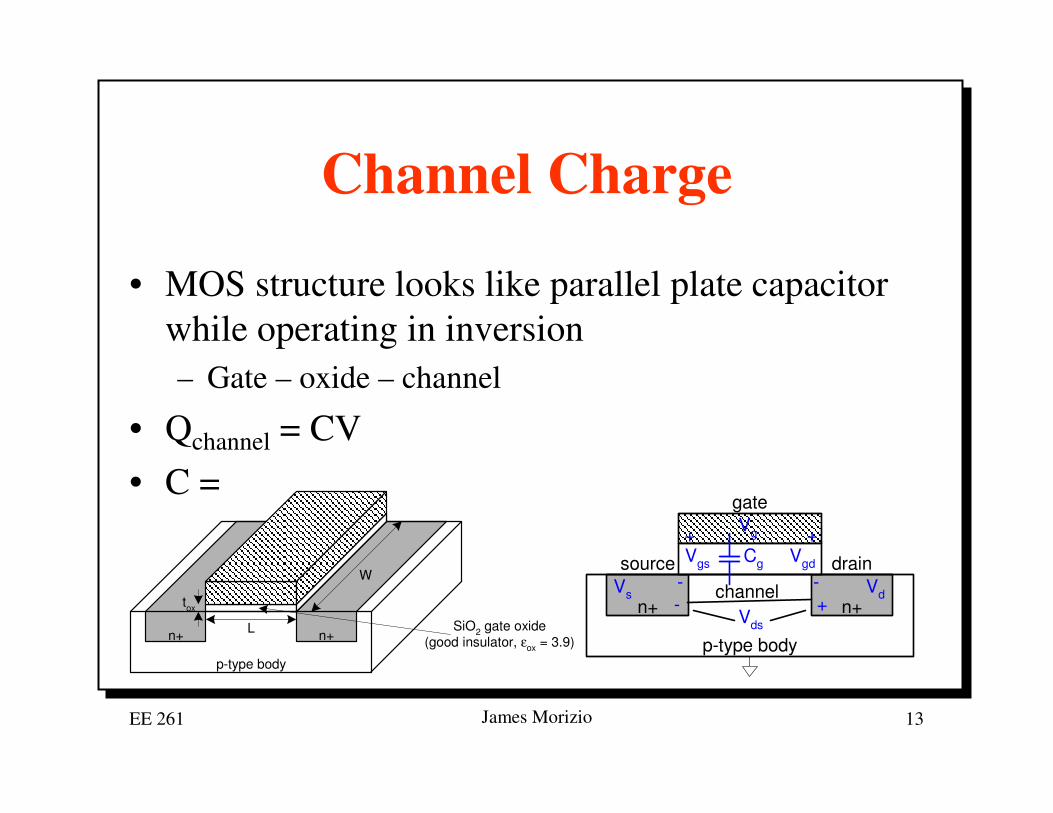
Channel Charge
• MOS structure looks like parallel plate capacitor while operating in inversion– Gate – oxide – channel
• Qchannel = CV• C =
n+ n+
p-type body
+
Vgd
gate
+ +source
-
Vgs
-drain
Vds
channel-
Vg
Vs Vd
Cg
n+ n+
p-type body
W
L
tox
SiO2 gate oxide(good insulator, εox = 3.9)
polysilicongate
EE 261 James Morizio 14
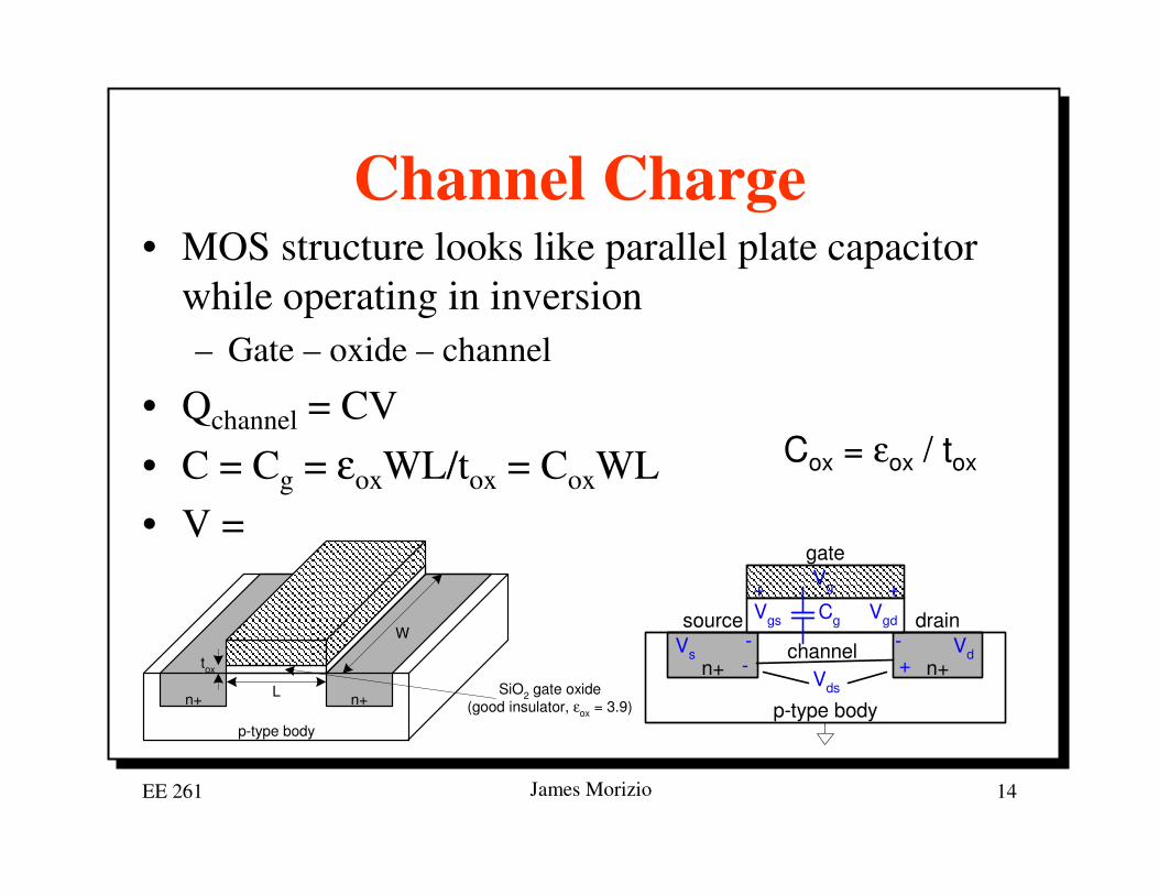
Channel Charge• MOS structure looks like parallel plate capacitor
while operating in inversion– Gate – oxide – channel
• Qchannel = CV• C = Cg = εoxWL/tox = CoxWL• V =
n+ n+
p-type body
+
Vgd
gate
+ +source
-
Vgs
-drain
Vds
channel-
Vg
Vs Vd
Cg
n+ n+
p-type body
W
L
tox
SiO2 gate oxide(good insulator, εox = 3.9)
polysilicongate
Cox = εox / tox
EE 261 James Morizio 15
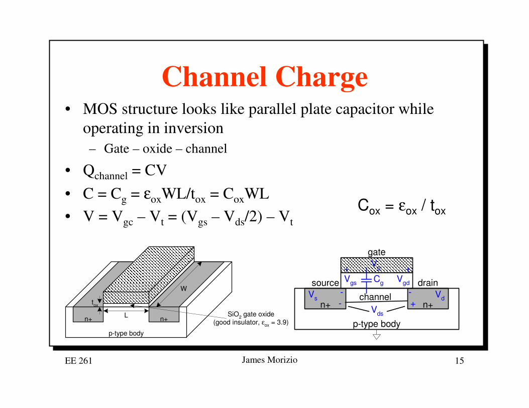
Channel Charge• MOS structure looks like parallel plate capacitor while
operating in inversion– Gate – oxide – channel
• Qchannel = CV• C = Cg = εoxWL/tox = CoxWL• V = Vgc – Vt = (Vgs – Vds/2) – Vt
n+ n+
p-type body
+
Vgd
gate
+ +source
-
Vgs
-drain
Vds
channel-
Vg
Vs Vd
Cg
n+ n+
p-type body
W
L
tox
SiO2 gate oxide(good insulator, εox = 3.9)
polysilicongate
Cox = εox / tox
EE 261 James Morizio 16
Carrier velocity
• Charge is carried by e-• Carrier velocity v proportional to lateral E-field
between source and drain• v =
EE 261 James Morizio 17
Carrier velocity
• Charge is carried by e-• Carrier velocity v proportional to lateral E-field
between source and drain• v = µE µ called mobility• E =

EE 261 James Morizio 18
Carrier velocity
• Charge is carried by e-• Carrier velocity v proportional to lateral E-field
between source and drain• v = µE µ called mobility• E = Vds/L• Time for carrier to cross channel:
– t =
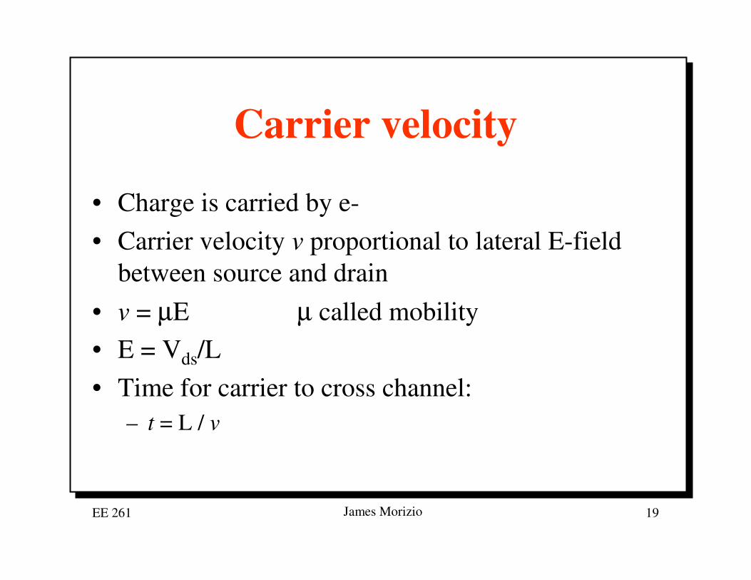
EE 261 James Morizio 19
Carrier velocity
• Charge is carried by e-• Carrier velocity v proportional to lateral E-field
between source and drain• v = µE µ called mobility• E = Vds/L• Time for carrier to cross channel:
– t = L / v
EE 261 James Morizio 20
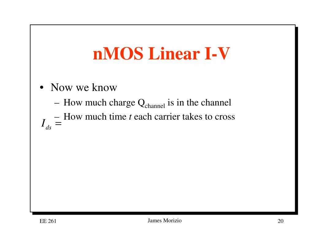
nMOS Linear I-V
• Now we know– How much charge Qchannel is in the channel– How much time t each carrier takes to cross
dsI =

EE 261 James Morizio 21
nMOS Linear I-V
• Now we know– How much charge Qchannel is in the channel– How much time t each carrier takes to cross
channelds
QI
t=
=

EE 261 James Morizio 22
nMOS Linear I-V• Now we know
– How much charge Qchannel is in the channel– How much time t each carrier takes to cross
channel
ox 2
2
ds
dsgs t ds
dsgs t ds
QI
tW VC V V VL
VV V V
µ
β
=
= − −
= − −
ox = W
CL
β µ

EE 261 James Morizio 23
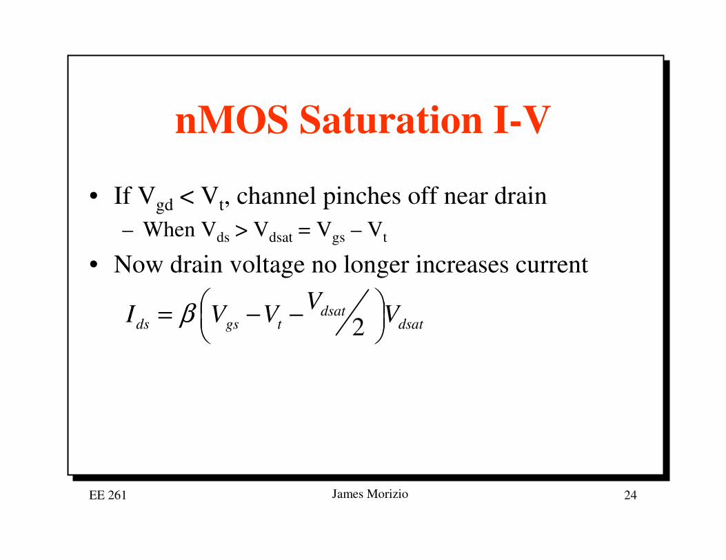
nMOS Saturation I-V
• If Vgd < Vt, channel pinches off near drain– When Vds > Vdsat = Vgs – Vt
• Now drain voltage no longer increases current
dsI =
EE 261 James Morizio 24
nMOS Saturation I-V
• If Vgd < Vt, channel pinches off near drain– When Vds > Vdsat = Vgs – Vt
• Now drain voltage no longer increases current
2dsat
ds gs t dsatVI V V Vβ = − −

EE 261 James Morizio 25
nMOS Saturation I-V
• If Vgd < Vt, channel pinches off near drain– When Vds > Vdsat = Vgs – Vt
• Now drain voltage no longer increases current
( )2
2
2
dsatds gs t dsat
gs t
VI V V V
V V
β
β
= − −
= −
EE 261 James Morizio 26
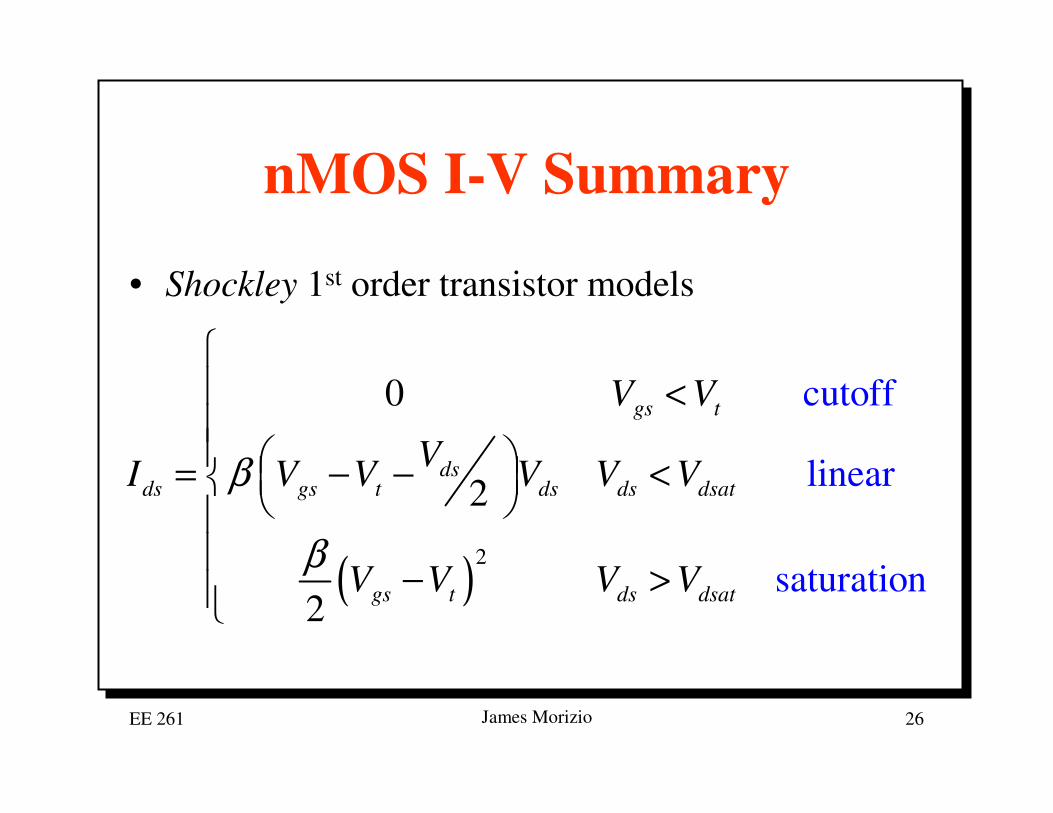
nMOS I-V Summary
( )2
cutoff
linear
saturatio
0
2
2n
gs t
dsds gs t ds ds dsat
gs t ds dsat
V V
VI V V V V V
V V V V
β
β
< = − − <
− >
• Shockley 1st order transistor models
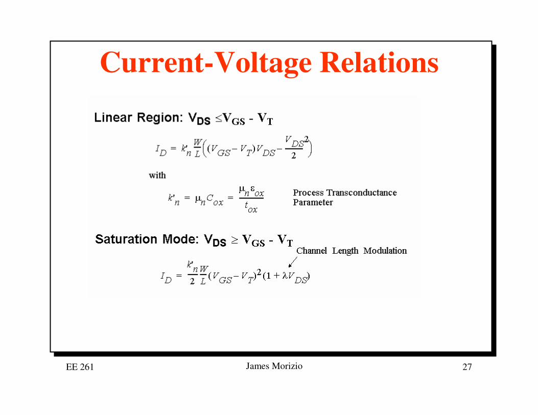
EE 261 James Morizio 27
Current-Voltage Relations
EE 261 James Morizio 28
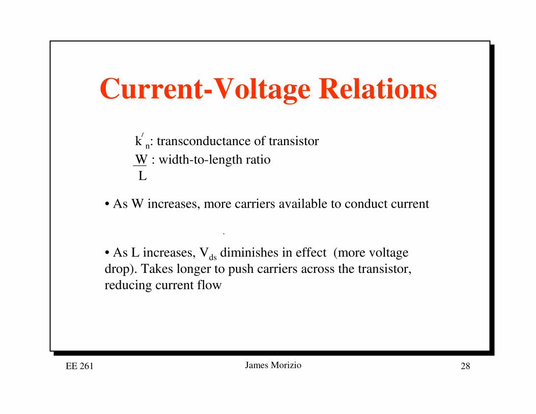
Current-Voltage Relationsk n: transconductance of transistorW : width-to-length ratioL
• As W increases, more carriers available to conduct current
• As L increases, Vds diminishes in effect (more voltage drop). Takes longer to push carriers across the transistor, reducing current flow
EE 261 James Morizio 29
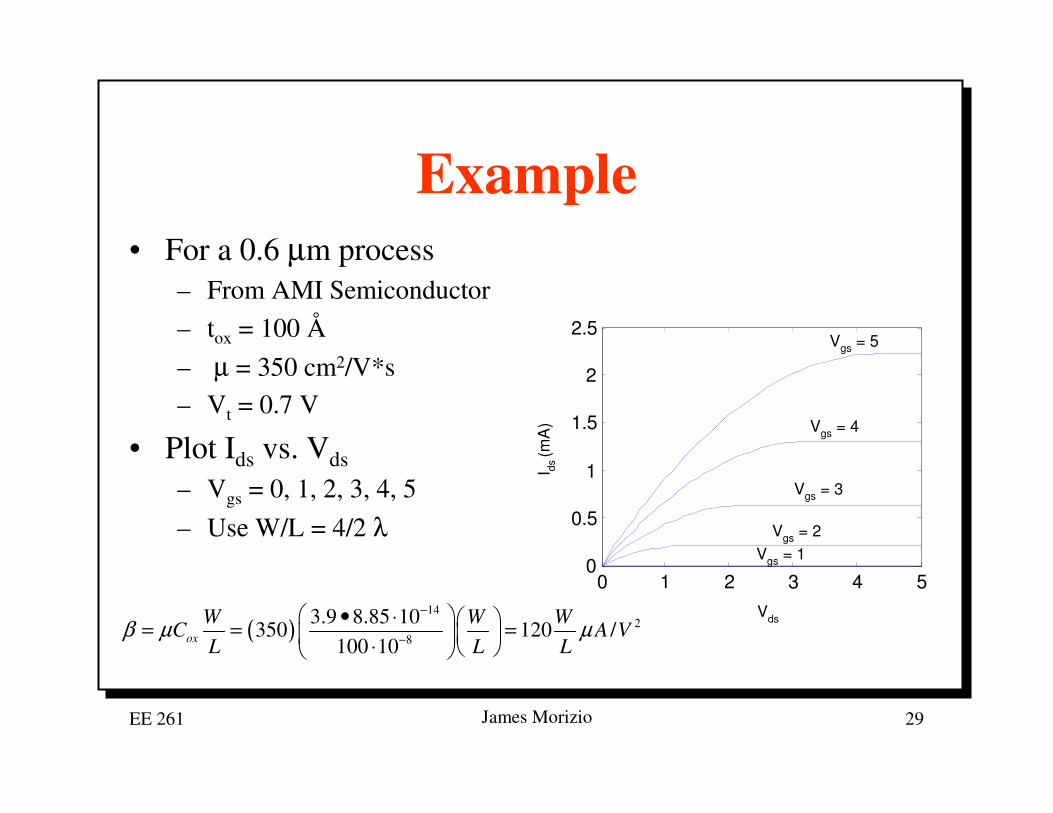
Example• For a 0.6 µm process
– From AMI Semiconductor– tox = 100 Å– µ = 350 cm2/V*s– Vt = 0.7 V
• Plot Ids vs. Vds– Vgs = 0, 1, 2, 3, 4, 5– Use W/L = 4/2 λ
( )14
28
3.9 8.85 10350 120 /
100 10ox
W W WC A V
L L Lβ µ µ
−
−
• ⋅ = = = ⋅
0 1 2 3 4 50
0.5
1
1.5
2
2.5
Vds
I ds (m
A)
Vgs = 5
Vgs = 4
Vgs = 3
Vgs = 2Vgs = 1

EE 261 James Morizio 30
pMOS I-V
• All dopings and voltages are inverted for pMOS• Mobility µp is determined by holes
– Typically 2-3x lower than that of electrons µn
– 120 cm2/V*s in AMI 0.6 µm process
• Thus pMOS must be wider to provide same current– In this class, assume µn / µp = 2 to 3
EE 261 James Morizio 31
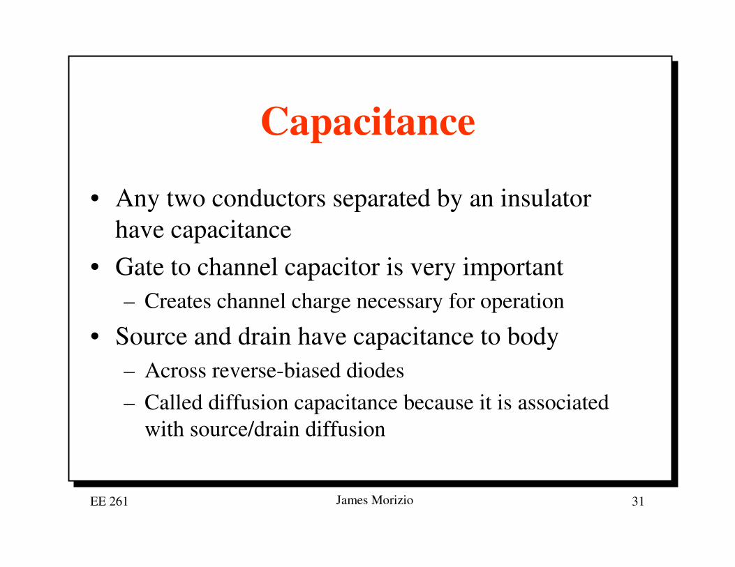
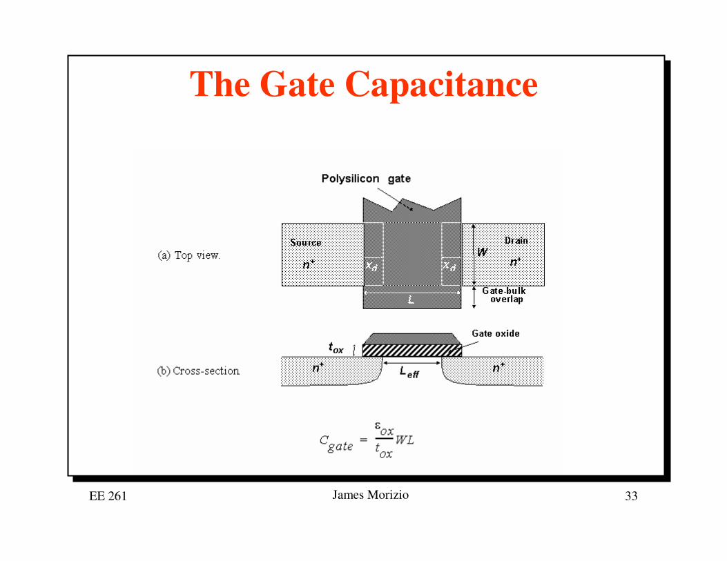
Capacitance
• Any two conductors separated by an insulator have capacitance
• Gate to channel capacitor is very important– Creates channel charge necessary for operation
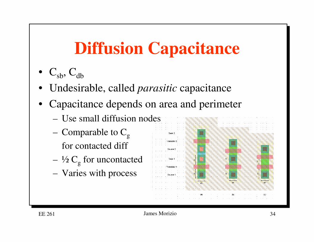
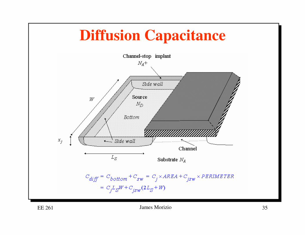
• Source and drain have capacitance to body– Across reverse-biased diodes– Called diffusion capacitance because it is associated
with source/drain diffusion
EE 261 James Morizio 32
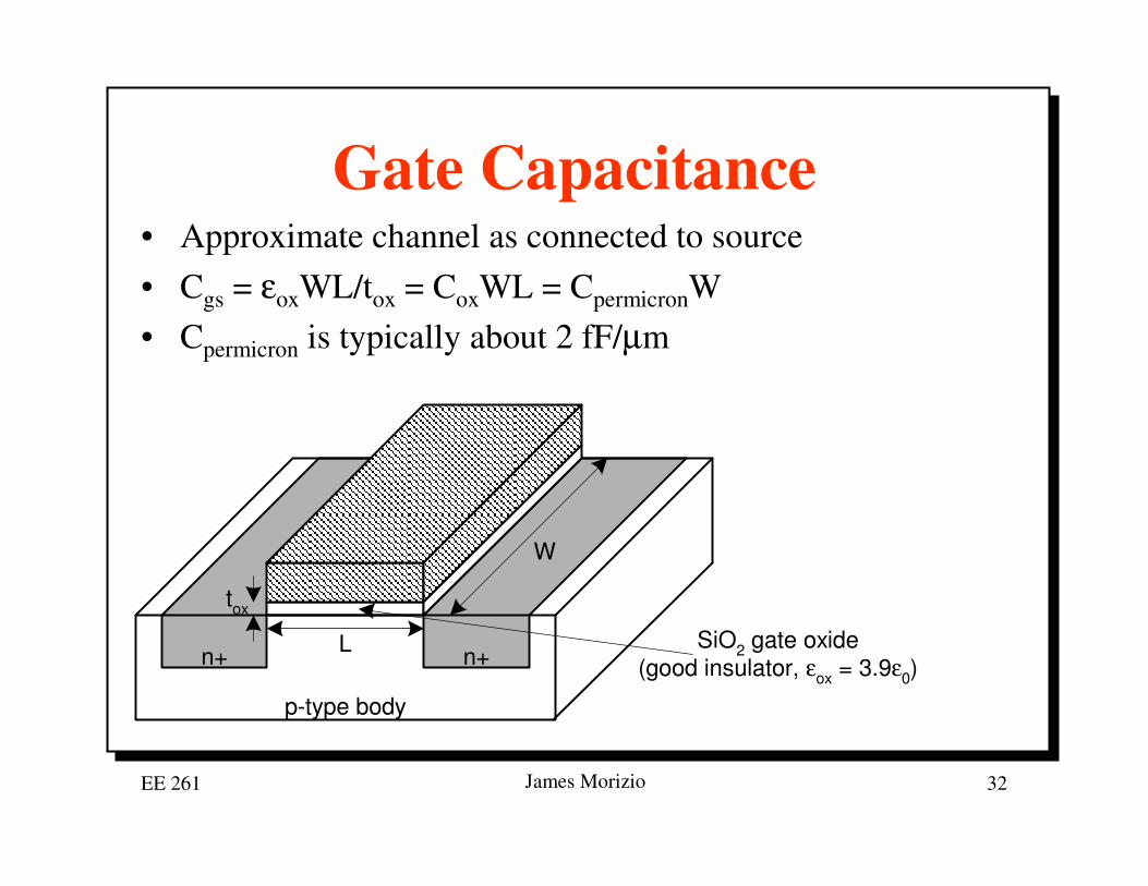
Gate Capacitance• Approximate channel as connected to source• Cgs = εoxWL/tox = CoxWL = CpermicronW• Cpermicron is typically about 2 fF/µm
n+ n+
p-type body
W
L
tox
SiO2 gate oxide(good insulator, εox = 3.9ε0)
polysilicongate
EE 261 James Morizio 33
The Gate Capacitance
EE 261 James Morizio 34
Diffusion Capacitance• Csb, Cdb
• Undesirable, called parasitic capacitance• Capacitance depends on area and perimeter
– Use small diffusion nodes– Comparable to Cg
for contacted diff– ½ Cg for uncontacted– Varies with process
EE 261 James Morizio 35
Diffusion Capacitance
EE 261 James Morizio 36
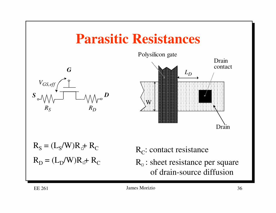
Parasitic Resistances
W
LD
Drain
Draincontact
Polysilicon gate
DS
G
RS RD
VGS,eff
RS = (LS/W)R + RC
RD = (LD/W)R + RC
RC: contact resistanceR : sheet resistance per square
of drain-source diffusion
EE 261 James Morizio 37
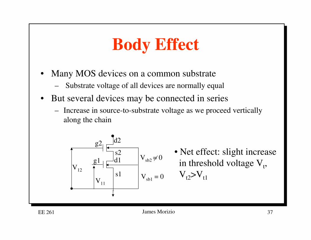
Body Effect• Many MOS devices on a common substrate
– Substrate voltage of all devices are normally equal
• But several devices may be connected in series– Increase in source-to-substrate voltage as we proceed vertically
along the chain
d1
d2
s1
s2
V12
V11
g1
g2
Vsb1 = 0
Vsb2 = 0• Net effect: slight increasein threshold voltage Vt,Vt2>Vt1

EE 261 James Morizio 38
Pass Transistors
• We have assumed source is grounded• What if source > 0?
– e.g. pass transistor passing VDD
VDDVDD

EE 261 James Morizio 39
Pass Transistors
• We have assumed source is grounded• What if source > 0?
– e.g. pass transistor passing VDD
• Vg = VDD– If Vs > VDD-Vt, Vgs < Vt
– Hence transistor would turn itself off
• nMOS pass transistors pull no higher than VDD-Vtn– Called a degraded “1”– Approach degraded value slowly (low Ids)
• pMOS pass transistors pull no lower than Vtp
VDDVDD
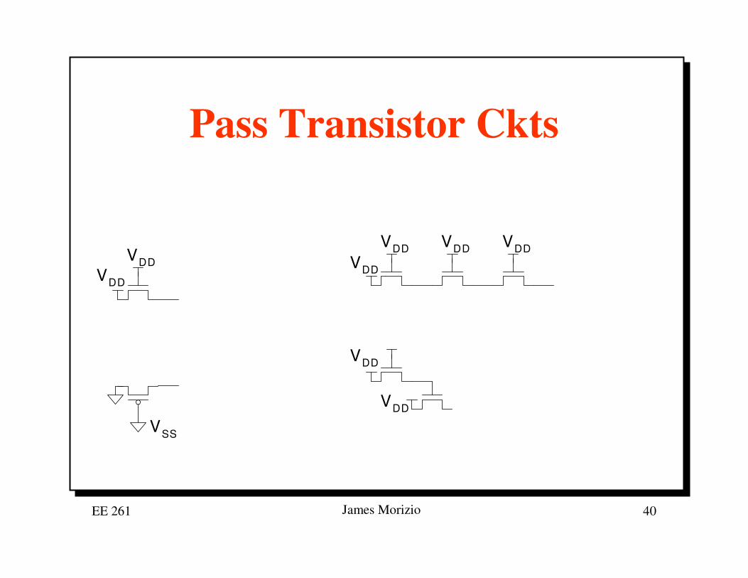
EE 261 James Morizio 40
Pass Transistor Ckts
VDDVDD
VSS
VDD
VDD
VDD VDD VDD
VDD
EE 261 James Morizio 41
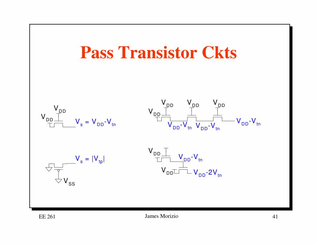
Pass Transistor Ckts
VDDVDD Vs = VDD-Vtn
VSS
Vs = |Vtp|
VDD
VDD-Vtn VDD-VtnVDD-Vtn
VDD
VDD VDD VDD
VDD
VDD-Vtn
VDD-2Vtn

EE 261 James Morizio 42
Effective Resistance
• Shockley models have limited value– Not accurate enough for modern transistors– Too complicated for much hand analysis
• Simplification: treat transistor as resistor– Replace Ids(Vds, Vgs) with effective resistance R
• Ids = Vds/R– R averaged across switching of digital gate
• Too inaccurate to predict current at any given time– But good enough to predict RC delay

EE 261 James Morizio 43
RC Delay Model• Use equivalent circuits for MOS transistors
– Ideal switch + capacitance and ON resistance– Unit nMOS has resistance R, capacitance C– Unit pMOS has resistance 2R, capacitance C
• Capacitance proportional to width• Resistance inversely proportional to width
kgs
d
g
s
d
kCkC
kCR/k
kgs
d
g
s
d
kC
kC
kC
2R/k
EE 261 James Morizio 44
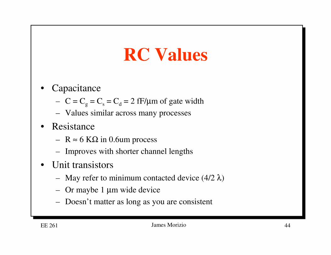
RC Values
• Capacitance– C = Cg = Cs = Cd = 2 fF/µm of gate width– Values similar across many processes
• Resistance– R ≈ 6 KΩ in 0.6um process– Improves with shorter channel lengths
• Unit transistors– May refer to minimum contacted device (4/2 λ)– Or maybe 1 µm wide device– Doesn’t matter as long as you are consistent
EE 261 James Morizio 45
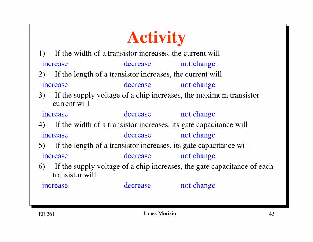
Activity1) If the width of a transistor increases, the current willincrease decrease not change
2) If the length of a transistor increases, the current willincrease decrease not change
3) If the supply voltage of a chip increases, the maximum transistor current will
increase decrease not change4) If the width of a transistor increases, its gate capacitance willincrease decrease not change
5) If the length of a transistor increases, its gate capacitance willincrease decrease not change
6) If the supply voltage of a chip increases, the gate capacitance of each transistor will
increase decrease not change

EE 261 James Morizio 46
Activity1) If the width of a transistor increases, the current willincrease decrease not change
2) If the length of a transistor increases, the current willincrease decrease not change
3) If the supply voltage of a chip increases, the maximum transistor current will
increase decrease not change4) If the width of a transistor increases, its gate capacitance willincrease decrease not change
5) If the length of a transistor increases, its gate capacitance willincrease decrease not change
6) If the supply voltage of a chip increases, the gate capacitance of each transistor will
increase decrease not change
EE 261 James Morizio 47
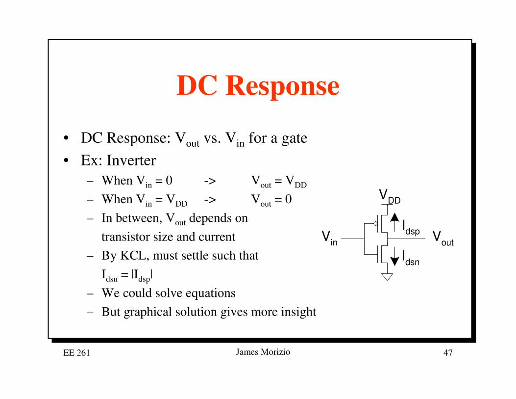
DC Response
• DC Response: Vout vs. Vin for a gate• Ex: Inverter
– When Vin = 0 -> Vout = VDD
– When Vin = VDD -> Vout = 0– In between, Vout depends on
transistor size and current– By KCL, must settle such that
Idsn = |Idsp|– We could solve equations– But graphical solution gives more insight
Idsn
Idsp Vout
VDD
Vin
EE 261 James Morizio 48
Transistor Operation
• Current depends on region of transistor behavior• For what Vin and Vout are nMOS and pMOS in
– Cutoff?– Linear?– Saturation?
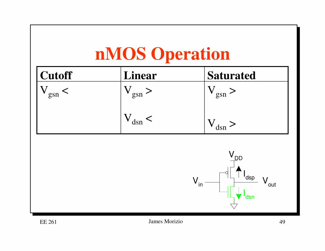
EE 261 James Morizio 49
nMOS Operation
Vgsn >
Vdsn >
Vgsn >
Vdsn <
Vgsn <SaturatedLinearCutoff
Idsn
Idsp Vout
VDD
Vin
EE 261 James Morizio 50
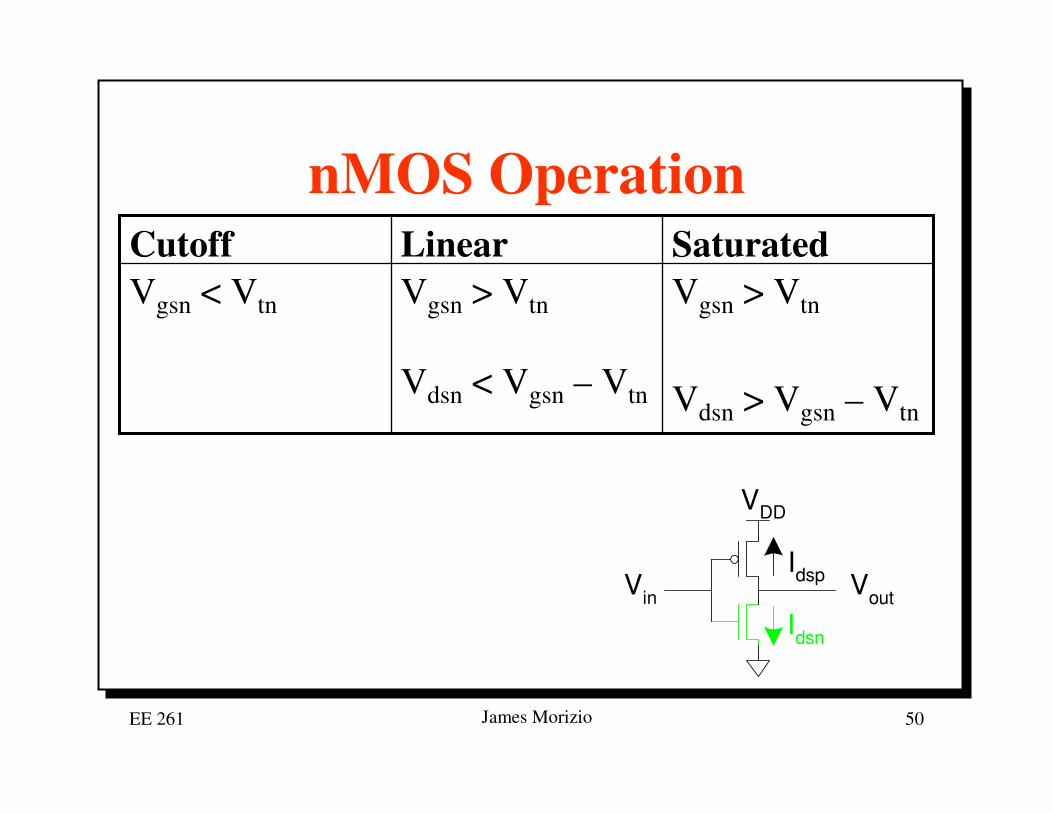
nMOS Operation
Vgsn > Vtn
Vdsn > Vgsn – Vtn
Vgsn > Vtn
Vdsn < Vgsn – Vtn
Vgsn < Vtn
SaturatedLinearCutoff
Idsn
Idsp Vout
VDD
Vin
EE 261 James Morizio 51
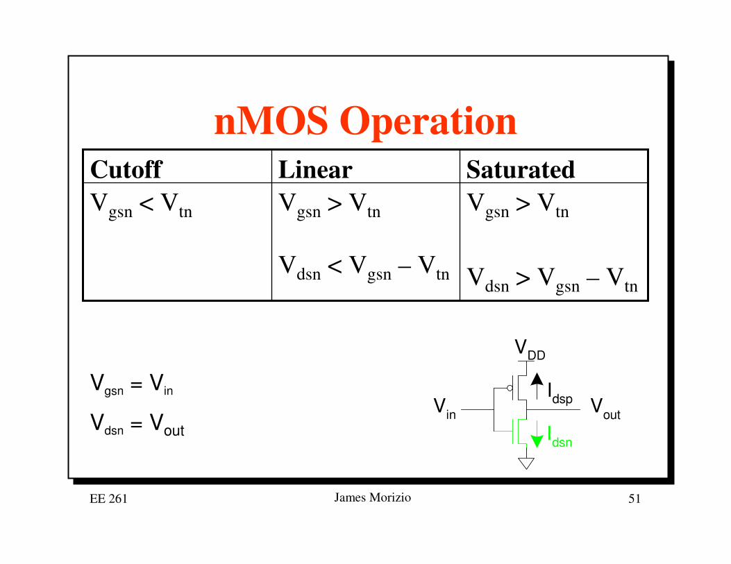
nMOS Operation
Vgsn > Vtn
Vdsn > Vgsn – Vtn
Vgsn > Vtn
Vdsn < Vgsn – Vtn
Vgsn < Vtn
SaturatedLinearCutoff
Idsn
Idsp Vout
VDD
Vin
Vgsn = Vin
Vdsn = Vout
EE 261 James Morizio 52
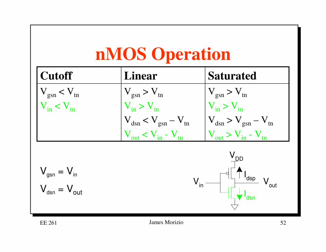
nMOS Operation
Vgsn > Vtn
Vin > Vtn
Vdsn > Vgsn – Vtn
Vout > Vin - Vtn
Vgsn > Vtn
Vin > Vtn
Vdsn < Vgsn – Vtn
Vout < Vin - Vtn
Vgsn < Vtn
Vin < Vtn
SaturatedLinearCutoff
Idsn
Idsp Vout
VDD
Vin
Vgsn = Vin
Vdsn = Vout

EE 261 James Morizio 53
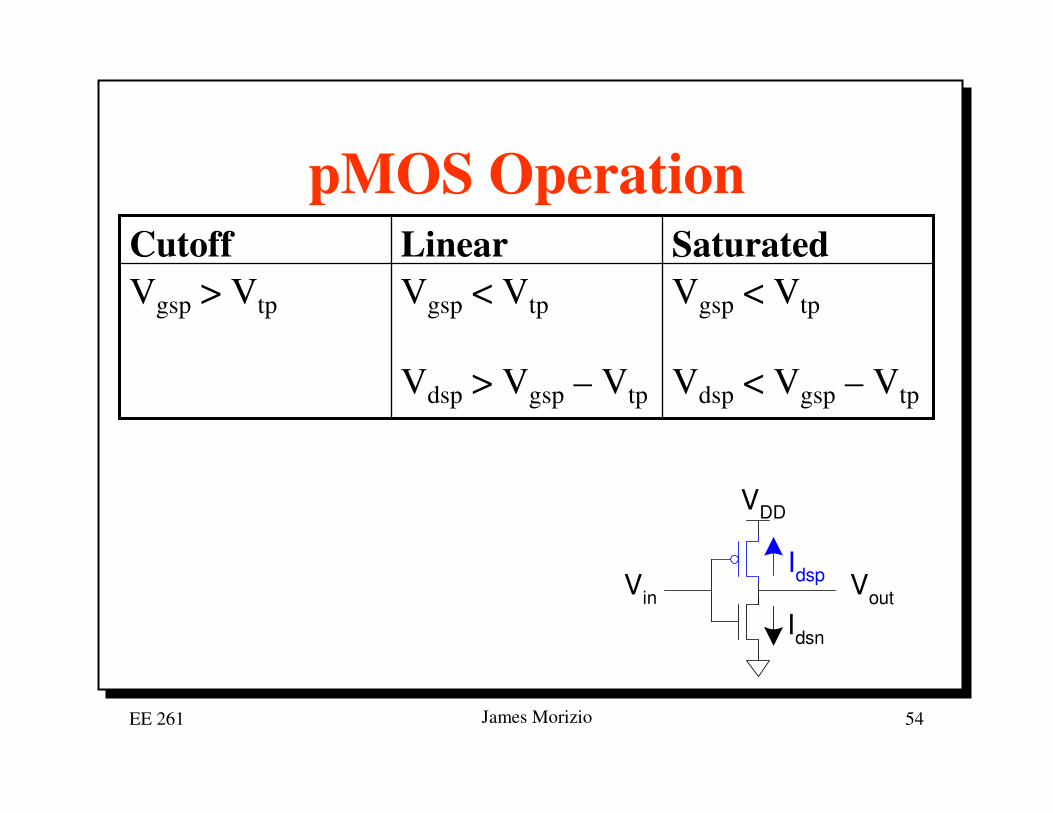
pMOS Operation
Vgsp <
Vdsp <
Vgsp <
Vdsp >
Vgsp >SaturatedLinearCutoff
Idsn
Idsp Vout
VDD
Vin
EE 261 James Morizio 54
pMOS Operation
Vgsp < Vtp
Vdsp < Vgsp – Vtp
Vgsp < Vtp
Vdsp > Vgsp – Vtp
Vgsp > Vtp
SaturatedLinearCutoff
Idsn
Idsp Vout
VDD
Vin

EE 261 James Morizio 55
pMOS Operation
Vgsp < Vtp
Vdsp < Vgsp – Vtp
Vgsp < Vtp
Vdsp > Vgsp – Vtp
Vgsp > Vtp
SaturatedLinearCutoff
Idsn
Idsp Vout
VDD
Vin
Vgsp = Vin - VDD
Vdsp = Vout - VDD
Vtp < 0

EE 261 James Morizio 56
pMOS Operation
Vgsp < Vtp
Vin < VDD + Vtp
Vdsp < Vgsp – Vtp
Vout < Vin - Vtp
Vgsp < Vtp
Vin < VDD + Vtp
Vdsp > Vgsp – Vtp
Vout > Vin - Vtp
Vgsp > Vtp
Vin > VDD + Vtp
SaturatedLinearCutoff
Idsn
Idsp Vout
VDD
Vin
Vgsp = Vin - VDD
Vdsp = Vout - VDD
Vtp < 0

EE 261 James Morizio 57
I-V Characteristics• Make pMOS wider than nMOS such that βn = βp
Vgsn5
Vgsn4
Vgsn3
Vgsn2Vgsn1
Vgsp5
Vgsp4
Vgsp3
Vgsp2
Vgsp1
VDD
-VDD
Vdsn
-Vdsp
-Idsp
Idsn
0
EE 261 James Morizio 58
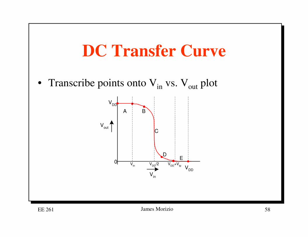
DC Transfer Curve
• Transcribe points onto Vin vs. Vout plot
CVout
0
Vin
VDD
VDD
A B
DE
Vtn VDD/2 VDD+Vtp
EE 261 James Morizio 59
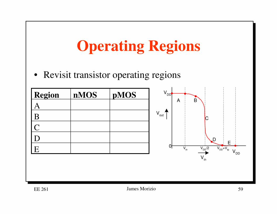
Operating Regions
• Revisit transistor operating regions
CVout
0
Vin
VDD
VDD
A B
DE
Vtn VDD/2 VDD+VtpEDCBA
pMOSnMOSRegion

EE 261 James Morizio 60
Operating Regions
• Revisit transistor operating regions
CVout
0
Vin
VDD
VDD
A B
DE
Vtn VDD/2 VDD+VtpCutoffLinearE
SaturationLinearD
SaturationSaturationC
LinearSaturationB
LinearCutoffA
pMOSnMOSRegion
EE 261 James Morizio 61
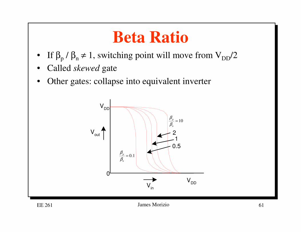
Beta Ratio• If βp / βn ≠ 1, switching point will move from VDD/2• Called skewed gate• Other gates: collapse into equivalent inverter
Vout
0
Vin
VDD
VDD
0.51
2
10p
n
ββ
=
0.1p
n
ββ
=
EE 261 James Morizio 62
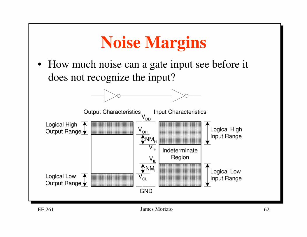
Noise Margins• How much noise can a gate input see before it
does not recognize the input?
IndeterminateRegion
NML
NMH
Input CharacteristicsOutput Characteristics
VOH
VDD
VOL
GND
VIH
VIL
Logical HighInput Range
Logical LowInput Range
Logical HighOutput Range
Logical LowOutput Range

EE 261 James Morizio 63
Logic Levels
• To maximize noise margins, select logic levels at
VDD
Vin
Vout
VDD
βp/βn > 1
Vin Vout
0
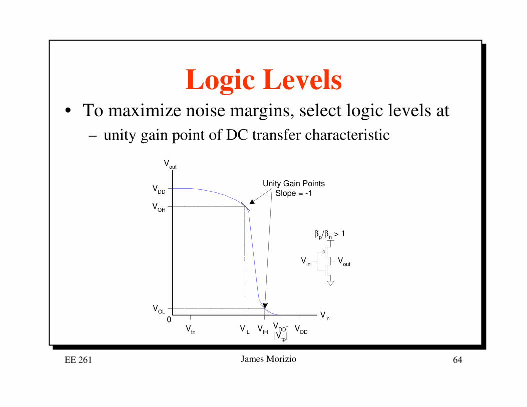
EE 261 James Morizio 64
Logic Levels• To maximize noise margins, select logic levels at
– unity gain point of DC transfer characteristic
VDD
Vin
Vout
VOH
VDD
VOL
VIL VIHVtn
Unity Gain PointsSlope = -1
VDD-|Vtp|
βp/βn > 1
Vin Vout
0
EE 261 James Morizio 65