DO IT YOURSELF - SCANNING TUNNELING MICROSCOPE41j.com/blog/wp-content/uploads/2014/09/paper.pdf ·...
33
Do It Yourself – Scanning Tunneling Microscope Kantonsschule Wettingen Maturaarbeit 2008/2009 Authors Sandro Merkli Ivan Ovinnikov Dominik Wild Advisers Wolfgang Mann Dr. Thomas Graf
Transcript of DO IT YOURSELF - SCANNING TUNNELING MICROSCOPE41j.com/blog/wp-content/uploads/2014/09/paper.pdf ·...

Do It Yourself –
Scanning Tunneling Microscope
Kantonsschule WettingenMaturaarbeit 2008/2009
Authors
Sandro MerkliIvan OvinnikovDominik Wild
Advisers
Wolfgang MannDr. Thomas Graf

Preface
Already half a year before the beginning of the Maturaarbeit, we had decidedwhat we wanted to do: to build our own scanning tunneling microscope. Theidea emerged when we heard that the physical assistant at our school, HansulrichSchmutz, had bought components to construct such a device. We thought it tobe an ideal project for several reasons. The practical work would set a contrastto school and it would be an opportunity to experience research and its creativeprocesses. Furthermore, we are all intrigued by sciences and technology.
We were aware of the fact that our enterprise did not promise definite success.Due to this circumstance, we set our minimal goal to be the following: measureand derive a function of the tunneling current depending on the distance betweenthe tip and the sample. We are glad to have reached this goal but we didnot succeed to accomplish our ultimate goal of a fully functioning microscope.However, we plan to continue our project and this work lays a solid base forthat. Thus, that we are looking forward to make quick progress. We are alsoparticipating in the Schweizer Jugend Forscht competition which sets a differenttime frame. The deadline set for the competition is a few months later than theMaturaarbeit’s deadline. This makes it possible for us to try and achieve ourfinal goals until then.
This paper should give an impression of our work and introduce the reader tothe topic of scanning tunneling microscopy. The first part covers the theoreticalbackground whereas the second part specifically documents our implementationof a scanning tunneling microscope. Both parts have their own introductionwhich will guide the reader. In the third part, we document and interpretthe results we have achieved so far. In addition to this paper, we acquired aninternet domain (www.stm-diy.ch).Under this address, we published a summaryof the work we’ve done and contact addresses for questions. For more detailedinformation, we provide a downloads section containing useful schematics.
We are greatly indebted to many people and organizations who supportedus in our work. The Paul Scherrer Institute, IBM Zurich, EMPA and Carl ZeissAG all contributed to our project with their generous financial aid. IBM Zurichand the Paul Scherrer Institut both offered their help in technical concerns.The co-operation with the Paul Scherrer Institut turned out to be extremelyhelpful and we owe special thanks to Jan Hovind, Siegfried Ebers, Dr. ThomasJung and Valeri Ovinnikov, Ivan’s father. He spent a lot of time designing thecontrol electronics, a task not fulfillable for us. Finally, we have to expressour gratitude to Hansulrich Schmutz. His experience, explanations and effortwere of inestimable value and confirmed us in our enthusiasm. Martin Merkli,Sandros father, helped a lot in the acquisition of non-standard materials usedfor the mechanical setup, and provided a car, making us a lot more mobile andtime-efficient.

CONTENTS
Contents
I Theoretical Treatment 4
1 Introduction 5
2 Quantum Tunneling 6
3 Piezoelectric elements 103.1 The piezoelectric effect . . . . . . . . . . . . . . . . . . . . . . . . 103.2 Scanner Types . . . . . . . . . . . . . . . . . . . . . . . . . . . . 11
4 Electronics 114.1 Amplification . . . . . . . . . . . . . . . . . . . . . . . . . . . . . 114.2 Control Electronics . . . . . . . . . . . . . . . . . . . . . . . . . . 13
5 Vibration Isolation 15
6 Tip Preparation 15
II Documentation 16
7 Initial Approach 177.1 Mechanical Build . . . . . . . . . . . . . . . . . . . . . . . . . . . 177.2 Tunneling Current Amplifier . . . . . . . . . . . . . . . . . . . . 177.3 Scanning Electronics . . . . . . . . . . . . . . . . . . . . . . . . . 18
8 Difficulties 218.1 Vibration Damping . . . . . . . . . . . . . . . . . . . . . . . . . . 218.2 Acoustic Noise . . . . . . . . . . . . . . . . . . . . . . . . . . . . 218.3 Tunneling Current Amplifier . . . . . . . . . . . . . . . . . . . . 228.4 Control Electronics . . . . . . . . . . . . . . . . . . . . . . . . . . 23
9 Current Design 24
10 Future plans 2510.1 Mechanical Build . . . . . . . . . . . . . . . . . . . . . . . . . . . 2510.2 Control Electronics . . . . . . . . . . . . . . . . . . . . . . . . . . 25
III Experimental Results 26
11 Methods 26
12 Results 27
Conclusion 31
2

LIST OF FIGURES
List of Figures
1 Schematic diagram of a STM . . . . . . . . . . . . . . . . . . . . 52 STM scan of a graphite surface . . . . . . . . . . . . . . . . . . . 63 Potential energy in a STM . . . . . . . . . . . . . . . . . . . . . . 74 Wavefunction of an electron in the sample . . . . . . . . . . . . . 75 Probability function . . . . . . . . . . . . . . . . . . . . . . . . . 96 Piezoelectric coefficients . . . . . . . . . . . . . . . . . . . . . . . 107 Scanner types . . . . . . . . . . . . . . . . . . . . . . . . . . . . . 118 A number of op-amps . . . . . . . . . . . . . . . . . . . . . . . . 129 Operational amplifier symbol . . . . . . . . . . . . . . . . . . . . 1210 Analog and digital feedback control . . . . . . . . . . . . . . . . . 1411 Our approach . . . . . . . . . . . . . . . . . . . . . . . . . . . . . 1712 Picture of our STM . . . . . . . . . . . . . . . . . . . . . . . . . . 1813 PIC32 Microprocessor Board . . . . . . . . . . . . . . . . . . . . 1914 Voltage converters . . . . . . . . . . . . . . . . . . . . . . . . . . 1915 P-CAD 2006 PCB Designer . . . . . . . . . . . . . . . . . . . . . 2016 Empty Printed Circuit Board . . . . . . . . . . . . . . . . . . . . 2017 Stands for the vibration damping . . . . . . . . . . . . . . . . . . 2118 Sound isolation box . . . . . . . . . . . . . . . . . . . . . . . . . 2219 The second and the third amplifier . . . . . . . . . . . . . . . . . 2320 Schematic of the third amplifier . . . . . . . . . . . . . . . . . . . 2321 The current design of the STM . . . . . . . . . . . . . . . . . . . 2422 The control electronics in the opened box . . . . . . . . . . . . . 2423 Computer-based measurement . . . . . . . . . . . . . . . . . . . . 2624 A good measurement . . . . . . . . . . . . . . . . . . . . . . . . . 2725 Current-position characteristic . . . . . . . . . . . . . . . . . . . 2826 A bad measurement . . . . . . . . . . . . . . . . . . . . . . . . . 30
3

I THEORETICAL TREATMENT
Part I
Theoretical TreatmentThis part covers the most important theoretical aspects of scanning tunnelingmicroscopy. Due to the variety of components in a scanning tunneling mi-croscope, the sections in this part are not continuous. For the same reason,the treatment of the single aspects remains rather qualitative. Nevertheless, itshould give the reader an insight to challenges and their technical solutions evenin topics he is not familiar with.
The introduction gives a short overview about scanning tunneling microscopyand explains the fundamental working of a STM. Section 2, Quantum Tunnel-ing, explores more precisely the physical principles underlying scanning tunnel-ing microscopy. The following four sections concentrate on technical aspects.Section 3, Piezoelectric elements, provides information about how the smallmovements of the tip can be realized, while section 4 is about the differentkinds of electronics which are required for read-out and control. The last twosections, Vibration Isolation and Tip Preparation, shortly comment on two fur-ther challenges.
The issues addressed are by no means exhaustive but we do not want to gointo more details. Our bibliography refers to relevant literature about scanningtunneling microscopy for further reading. Even these books refer to literatureabout specific topics as they cannot treat it sufficiently.
4

I THEORETICAL TREATMENT
1 Introduction
The STM is a powerful device to investigate surfaces and was invented in 1981by Gerd Binnig and Heinrich Rohrer at the IBM research center in Ruschlikon.Binnig and Rohrer were awarded the Nobel Prize in Physics for this inventionin 1986. Figure 1 illustrates the functioning of the STM. A very sharp probe –in the best case, there is a single atom at the end – scans the surface from a verysmall distance, usually in the order of an atomic diameter. The scanning motionis controlled with piezoelectric elements (3 Piezoelectric elements, page 10). Dueto a quantum physical phenomenon called tunneling effect, the voltage betweenprobe and sample leads to a very small current (2 Quantum Tunneling, page 6).Information about the surface can be obtained by measuring this current as itdepends on electrical properties of the sample and on the distance between thetip of the probe and the sample.
In general, there are two ways to scan a surface. Either the vertical positionof the probe or the current is kept constant. The former only works on very flatsurfaces but allows a high scanning speed. It is mainly used to study dynamicprocesses. The latter requires a feedback circuit to adjust the vertical positionof the tip such that there is no risk that the tip could crash into the sample. Atthe end, an image is generated from the x-y-z-coordinates of the tip (constantcurrent) or the x-y-coordinates and the current (constant distance). Good STMscan even resolve single atoms. Figure 2 shows an image of a graphite surfacewith atomic resolution.
There are other applications of the STM such as tunneling spectroscopywhich is out of the scope of this project. STMs only work on conducting sur-faces. The are other microscopes of the same type, the family of scanning probemicroscopes, which can scan non-conducting surfaces. The most important onein this family is the atomic force microscope. The principle of scanning is thesame but it measures force, rather than current.
Figure 1: Schematic diagram of a STM. http://en.wikipedia.org/wiki/Image:ScanningTunnelingMicroscope_schematic.png (January 8, 2009)
5

I THEORETICAL TREATMENT
Figure 2: STM scan of a graphite surface with atomic resolution.http://de.wikipedia.org/w/index.php?title=Bild:Graphite_ambient_STM.jpg
(January 8, 2009)
2 Quantum Tunneling
In order to understand the tunneling effect, we first consider the classical be-havior of particles. As a simplification we use a one-dimensional model. Themotion of a particle with energy E in a potential Epot(z) is described by
Ekin =12mv2 = E − Epot(z) ,
where m is the mass and v the velocity of the particle. v has a real result forE−Epot(z) ≥ 0. Therefore an area with potential Epot > E is impenetrable byclassical laws.
At the beginning of the 20th century, quantum mechanics revolutionized thephysical understanding of matter. On the one hand it was found out that lightdid not only show wave-like behavior. Rather it had to be described as a streamof particles, the photons, to explain some experiments. On the other handexactly the opposite was stated for particles. All matter has a wave-like nature.This statement is called De Broglie hypothesis in honor to Louis de Broglie whostated it in his PhD thesis in 1924 and received the Nobel Prize in Physics in1927 for his work. The wavelength of matter waves is described by the equation
λ =h
p.
h is Planck’s constant having the value 6.626069 ·10−34 J s and p is the particle’smomentum. The equation tells us why the wave-like behavior of matter cannotbe observed in everyday life. Let us take the example of a tennis ball weighing57g and flying at a speed of 40 m
s . We get a result of λ = 2.906 ·10−34 m which isfar too small that any effect caused by the wave-like nature would be observable.However on small scales or very low temperatures it is measurable and definitelynot negligible. Many phenomena on atomic scale, such as the tunneling effect,can only be explained with the help of quantum mechanics.
A particle in quantum mechanics is described by the wavefunction ψ(z) sat-isfying the Schrodinger equation. The Schrodinger equation was postulated in1926 by the Austrian physicist Erwin Schrodinger. It is a differential equation,which means it states a relationship between a function and its derivative. Actu-ally, the Schrodinger equation is a second order differential equation, containingthe second derivative.
6

I THEORETICAL TREATMENT
d2ψ(z)dz2
= −2m~2
(E − Epot)ψ(z)
is the so-called time-independent version of the Schrodinger equation. ~ = h2π =
1.054 · 10−34 Js is a constant often used to simplify equations. The time depen-dent version, often denoted as Ψ, is more complex (also in the mathematicalsense of the word) but it is not required in order to understand the tunnelingeffect. There is a relation between the wavefunction and the probability forthe particle to stay in a certain region of space. The continuous probabilitydistribution P (z) equals the wavefunction squared.
P (z) = (ψ(z))2
Applying the Schrodinger equation, it is possible to calculate the wavefunc-tion of an electron in a model similar to the situation in a STM. We take thepotential of the probe as point of reference. The electrons have a positive energyof E since they are moving in the solid. φ is the work function of the material.It is defined as the minimum energy required to remove an electron from thematerial [1]. E is smaller than φ because otherwise the electrons would not bebound to the metal. Figure 3 shows a graph of this situation.
φ
Energy
zSample
Epot
Vacuum Tip
E
Figure 3: Potential energy in a STM. Own illustration.
ψ
z
Figure 4: Wavefunction of an electron in the sample. Own illustration.
7

I THEORETICAL TREATMENT
The Schrodinger equation has two principally different solutions. Figure 4shows how these solutions apply in the model of the STM.
ψ(z) = A cos (kz + δ) if E − Epot > 0
k2 =2m~2
(E − Epot)
ψ(z) = Be−κz if E − Epot < 0
κ2 =2m~2
(Epot − E)
We do not show how to derive these results. Nevertheless, one can easily ver-ify them by putting ψ back into the Schrodinger equation. We denote thewavefunction in the sample, the vacuum and the tip as ψ1(z), ψ2(z) and ψ3(z),respectively. ψ depends on the amplitude A and the phase shift α. Analogously,ψ3 depends on C and β. As a fifth parameter, there is B in ψ2. These five pa-rameters can be reduced to one, here A, considering the constraint that thecomplete wavefunction of the electron has to be continuous. The first two con-ditions are received by equating the functions at the points where they meet,the other two by equating the derivatives. The gap between sample and tipbegins at z = 0 and ends at z = d.
ψ1(z) = A cos (kz + α)
ψ2(z) = Be−κz
ψ3(z) = C cos (kz + β)
A cos (α) = B (I)−kA sin (α) = −κB (II)
Be−κd = C cos (kd+ β) (III)
−κBe−κd = −kC sin (kd+ β) (IV)
tan (α) =κ
k(II) : (I)
tan (kd+ β) =κ
k(IV) : (III)
α = kd+ β = arctanκ
k
β = arctanκ
k− kd
B = A cos (α) = A cos(
arctanκ
k
)= A
k√k2 + κ2
C =B
cos (kd+ β)e−κd =
B
cos (α)e−κd = Ae−κd
8
I THEORETICAL TREATMENT
ψ1(z) = A cos(kz + arctan
κ
k
)ψ2(z) = A
k√k2 + κ2
e−κz
ψ3(z) = Ae−κd cos(kz + arctan
κ
k− kd
)Astonishingly the wavefunctions are not zero, neither in the tip nor in the vac-uum. This means that it is possible that an electron from the sample overcomesthe barrier and tunnels to the probe. Figure 5 shows the probability functionof the electron. Although small, there is a probability that the electron stays inthe tip. It can be seen from the result for ψ3(z) that the tunneling probabilityis proportional to e−2κd, the amplitude of the probability function in the tip.By classical laws the crossing of the barrier is not possible. Tunneling cannotbe explained by classical physics but only by quantum mechanics.
ψ2
z
Figure 5: The probability function of the electron in Figure 4. Own illustration.
Still there is no measurable current without a voltage applied because elec-trons tunnel equally from the tip to the sample and vice versa. With a voltageone side is put onto a higher potential. The electrons on this side have a greaterprobability to tunnel than the ones in the lower potential. This results in anet current which is measured in a STM. The current is proportional to theprobability of tunneling.
I ∝ e−2κd
A typical value for Epot,vac − E = φ (the work function) is 5 eV [11]. Togetherwith the electron mass m = 9.109 · 10−31 kg, we can use this value to calculatea numerical estimate for the decrease of the tunneling current with distance.
κ =√
2mφ~
= 1.146 · 1010 1m
For a distance d of 1A (10−10 m), this gives for the current
I ∝ e−2κd = e−2.291 =1
9.886.
Thus, the current decreases by roughly one order of magnitude per 1A. Thisvalue is only true in the vacuum. In air, the workfunction is much smallerbecause water condensates on the probe and tip (see section 12 for more infor-mation).
9

I THEORETICAL TREATMENT
3 Piezoelectric elements
3.1 The piezoelectric effect
The piezoelectric effect is a property of certain crystals and ceramics. If piezo-electric materials are compressed, an electric field in direction of the actingforce occurs. This effect is called the direct piezoelectric effect. The conversepiezoelectric effect is the elongation of a material if a voltage is applied. Pierreand Jacques Curie were the first to demonstrate the piezoelectric effect in 1880[7]. Quartz is an example of a piezoelectric material and it is widely used inwatches and clocks as oscillator. Another well-known application are piezoelec-tric crystals as igniter of lighters. A hammer hits the crystal thereby producinga voltage of thousands of volts which creates a spark [7].
In a STM, stacks of piezoceramics are used to control the position of theprobe. Such piezostacks consist of layers of a piezoceramic material with elec-trodes separating the layers. The single layers are therefore serially coupledand the effect is amplified. There are two important constants describing theproperties of piezoelectric materials. Figure 6 shows a piezoelectric element ina homogeneous electric field E3 parallel to the z-axis. The element not onlyexpands along the z-axis but also contracts in x-direction. The relative changesin length are
S1 = Sx =∆xx
S3 = Sz =∆zz.
x
z
x + ∆x
z+
∆z
Ez (E3)
Figure 6: Illustration of the piezoelectric coefficients. Own illustration (inspiredby [1]).
In the standard convention x, y, z are labeled with 1, 2 and 3. The so-calledpiezoelectric coefficients are the relative expansion divided by the electric field.The first number of the index is the direction of the field, the second one thedirection of the expansion.
d31 =S1
E3
d33 =S3
E3
10

I THEORETICAL TREATMENT
Using the relation E3 = Uz we get
∆x = d31 Ux
z∆z = d33 U
3.2 Scanner Types
Two scanner types used in STMs are worth to be mentioned. The tripod scannerconsists of three piezoelectric bars arranged in a tripod. It was implemented inthe first STM by Binnig and Rohrer and is still used in some home-built STMs.A tube scanner is a piezoelectric tube with four electrodes on the outer andone on the inner side. It can be bent by applying a voltage to two oppositeelectrodes. The elongation (z-direction) is controlled using the fifth electrodeinside the tube. The tube has several advantages over the tripod scanner and istherefore more often used in professional microscopes. The resonance frequencyof tube scanners is higher than the one of tripod scanners and, in addition, itis simpler in operation.
Figure 7: The tripod and the tube scanner. Own illustration.
4 Electronics
4.1 Amplification
The small tunneling current, in the order of pico- to nanoamps, needs to beamplified to be measurable. The current should also be converted into into avoltage since voltages are less sensitive to noise and can be easier processed.An amplifier that transforms a current into a voltage is called transimpedanceamplifier. A technical solution is offered by operational amplifiers (op-amps).
4.1.1 Operational Amplifiers
Op-amps are electronic components available in all different colors and shapes(Figure 8). Standard op-amps are a mass product and therefore very cheap.Op-amps with the specifications required for the application in a STM are moreexpensive but there is still a number of products to choose from, different man-ufacturers included. Due to the versatility of op-amps, they are used in a vastarray of devices.
Figure 9 shows the circuit board symbol of an op-amp with its most impor-tant pins. Us+ and Us− are the power supply pins. The voltage at the pins isvery often ±15 V, which also defines the maximum output voltage. U+ and U−
11

I THEORETICAL TREATMENT
Figure 8: A number of different op-amps. http://upload.wikimedia.org/
wikipedia/commons/0/06/OPAMP_Packages.jpg (January 8, 2009)
are the non-inverting and the inverting inputs respectively. Uout is the outputpin. In an ideal op-amp the input resistance, the resistance between U+ andU−, is infinite, so is the gain factor G. The output resistance is zero. Thesevalues are practically impossible but the properties of real op-amps are actuallyclose to the ideal ones.
Iin
Rfb
Uout
U
U
UoutU
U
−
+
s−
s+
Figure 9: The circuit board symbol of an op-amp (left) and an op-amp as a cur-rent amplifier (right). Modified from http://upload.wikimedia.org/wikipedia/
commons/9/97/Op-amp_symbol.svg (23.11.2008)
An op-amp as shown on the left hand side of Figure 9 amplifies the inputvoltage U+ − U− by the gain factor G.
Uout = (U+ − U−)G
This is useless since G is very high and weak noise is already amplified to themaximum output voltage. However, there are many different op-amp circuitssuch as the logarithmic or the differential amplifier which render the op-ampso flexible. Most relevant for the application in a STM is the transimpedanceamplifier or current amplifier also shown in Figure 9. The working of this circuitcan be derived from Kirchhoff’s laws but at this place, a good approximationshall be enough. From [1]:
To a very good approximation, the output voltage should pro-vide a feedback current through the feedback resistance Rfb to com-pensate the input current such that the net current entering theinverting input of the op-amp is zero. The non-inverting input isgrounded, and the voltage at the inverting input should be equal toground. This implies
UOUT = −IINRFB
12

I THEORETICAL TREATMENT
A common value forRfb in order to achieve sufficient amplification is 100 MΩ.This gives a gain factor of 0.1 V
nA . A gain of 1 VnA is often desirable [1]. Since
feedback resistances greater than 100 MΩ may cause technical problems, theamplification is often implemented as a cascade of two amplifiers.
There are other issues regarding amplification such as noise and frequencyresponse. All of these topics are thoroughly covered in [1]. It is important toknow that noise and other technical aspects, for instance parasitic capacities,are limiting factors of the amplifier.
4.2 Control Electronics
The amplified signal from the tunneling amplifier has to be read out and theposition of the z-piezo must be adapted accordingly if running the STM inconstant current mode. Principally, there exist two different implementationsof such a feedback loop, an analog and a digital one. Figure 10 shows a schematicdrawing of two such implementations.
The analog feedback circuit consists of a logarithmic amplifier and somefeedback electronics which compare the output signal to a set-point value andreturn a signal to the high voltage amplifier driving the piezos. In the feedbackelectronics a differential amplifier amplifies the difference between the outputvoltage and a set-point value. This value is then integrated since the differencebetween the set-point current and the measured current refers to a deviationfrom the current position of the tip. Therefore the value of the differentialamplifier has to be added to the voltage at the z-piezo. This is exactly what isdone by an integrator. The logarithmic amplifier, the differential amplifier andthe integrator can all be realized as op-amp circuits, which makes the analogfeedback quite simple.
For a fully functional STM, the x- and y-piezos must be controlled as welland the signal must be read out. Both can be accomplished by different means.In the first STMs, the scanning signal was produced using function generators,nowadays computers in combination with a digital to analog converter (D/Aconverter) can take this task. The output signal is often read out using ananalog to digital converter (A/D converter) but it could also be analyzed withsimpler means such as an oscilloscope.
In a digitally controlled feedback, all the steps after the current amplifierare replaced by an A/D converter, D/A converter and a computer, usually amicrocontroller. The signals from the current amplifier are converted to digitalsignals and registered by the microcontroller. They can be later transmittedto a personal computer. The microcontroller compares the value to a set-pointvalue and returns a corresponding voltage to the high voltage amplifier via aD/A converter.
The great advantage of digital implementation is its versatility. Other pa-rameters such as the x- and y-piezos and the bias voltage can be controlled usingthe same platform. Modifications of the scanning procedure can be controlledby software. However, it is more complicated than an analog implementationsand especially the speed of the platform can pose a problem. The real-timerequirements ask for special solutions, i.e. a microcontroller, and are hard tofulfill with a PC.
An effect to be considered in both approaches is the delay in response of thesystem. There is a delay in every amplifier, in the converters and in the mi-
13

I THEORETICAL TREATMENT
crocontroller. Neither do the piezos respond instantaneously due to mechanicalinertia. Therefore, the gain of the feedback circuit cannot be chosen arbitrarilyhigh. If the gain is chosen too high, the tip moves to its new position whilethe position is corrected even more so that at the end the tip is too far awayor too close. The whole process starts into the other direction. The response isunderdamped and the tip oscillates. It is easiest to find the critical damping byexperiment.
HighVoltageAmplifier Feedback
Electronics
LogarithmicAmplifier
CurrentAmplifier
x-piezoy-piezoz-piezo
OutputSignal
SetPoint
ScanningSignal
TunnelingCurrent
Analog feedback control
HighVoltageAmplifier
D/AConverter
A/DConverter
CurrentAmplifier
x-piezoy-piezoz-piezo
Bias Voltage
TunnelingCurrent
Digital feedback control
Figure 10: Typical implementations of analog and digital feedback control. Ownillustration (inspired by [1]).
14

I THEORETICAL TREATMENT
5 Vibration Isolation
In order to achieve high resolution, the STM should be insensitive to externalvibrations. The sources of vibrations can be various, from acoustic noise to astreet running nearby. Therefore, the required damping also depends on theenvironmental circumstances. Without any calculation, one can understandthat a rigid design is the most important factor in vibration isolation. Thevibrations do not influence the measurement if all parts of a STM vibrate atthe same frequency and amplitude. Springs together with a viscous damper,the damping force is proportional to the speed of the spring, can be completelysufficient. Sometimes, in a very quiet environment, no damping at all is required.Two stage systems can provide even better damping but the overall gain inperformance is limited so the focus should be on a rigid design. There are manydifferent approaches to vibration isolation, some of them dedicated to specialworking conditions such as ultra high vacuum. Exploring their advantages anddisadvantages would incorporate long calculations with doubtable success sincemany insights are based on experimental experience.
6 Tip Preparation
Ideally, there should be a single atom at the end of the tip to achieve maximumresolution. This proves to be less critical in experiment than expected. Since thetunneling current shows an exponential behavior, a single atom being a bit closerto the surface than others is responsible for most of the current flowing. Mosttips are made of a Platinum-Iridium alloy or of tungsten. Platinum-Iridiumdoes not easily oxidate and is therefore often used under ambient air conditions.The tips can be prepared using a side cutter, half drawing, half cutting under anacute angle. Tungsten tips are sometimes etched which gives a better controlover the resulting tip. Another suitable way to get a good tip is to apply arelatively high voltage between tip and sample while scanning which draws asingle atom out of the surface which is than attached to the tip.
Even with a seemingly good tip, atomic resolution is not always given. Itcan occur spontaneously during a scan, even after a crash with the surface.
15

II DOCUMENTATION
Part II
DocumentationThe documentation of our work illustrates our implementation and process toachieve it. In this documentation we follow a structure which aims to empha-size the process of improvement and problem solving. In the section InitialApproach, we explain our initial plans how to build the STM. This part isheld relatively short concerning the mechanics whereas the complexity of theelectronics require a longer introduction. As expected, various difficulties arosein the course of our work. The attempt to minimize their negative influences,whether they were successful or not, were reason for changes in the design weused in the beginning. All these difficulties and changes are subject in the sec-ond section, Difficulties. The third section, Current Design, summarizes thestate after all the improvements made. As we are participating in the competi-tion hosted by Schweizer Jugend forscht and due to our personal ambition, theend of the Maturaarbeit is not the end of our work. Hence, our future plans arementioned in section 10, Future plans.
We hope this allows insight to our working process and perhaps even helpsother amateur STM-builders in their enterprise.
16

II DOCUMENTATION
7 Initial Approach
7.1 Mechanical Build
When building our STM, we initially kept really close to a reference designwe had found during our research on the internet [10]. The main reason forthis is that a full design of a microscope would simply require too much timeto realize. Figure 11a shows the body of our STM. The reference design isbased on a construction which contains two aluminium plates, one lying ontop of the other with a three-point support. All three heights can be adjustedvia fine approach screws. The scanning head is mounted between two of thescrews, with an adjustable distance to the line connecting the two. This designmakes the lever applied by the third screw at the back user-adjustable, which isconvenient. The coarse approach of the tip is done using the screw at the back.For oscillation damping, we intended to use a metal plate with a weight of about30 kg placed on a pneumatic tire semi-filled with air (Figure 11b). A simplecardboard box with cone foam isolation was supposed to acoustically isolate themicroscope.
All mechanical parts, safe for the two parts of the scanning head, were man-ufactured by us at school. Material and instructions on how to use the machinewere provided by the school’s assistant of the physics department, HansulrichSchmutz, who soon became our main consultant in terms of mechanical parts.Due to their diminutive size, production of the scanning head parts had to beoutsourced to Jan Hovind from PSI. The heavy metal plate was bought in astore in Wettingen pointed to by Martin Merkli. The actual use of such platesis to close pipes that will be under pressure. As the plate was very dirty, wesent it to galvanizing using a contact of Martin Merkli’s. The wooden board waseasily obtained at a local do-it-yourself store and cut down to size at purchase.
(a) Mechanical build (b) Vibration damping
Figure 11: Two pictures illustrating our approach. Own pictures.
7.2 Tunneling Current Amplifier
At the beginning of our experiments, we used an amplifier which we had receivedfrom Siegfried Ebers, an electronics engineer at PSI. The amplifier was designedto amplify signals from photodiodes in order to detect radioactive radiation.Both the amplification of the tunneling current and of photodiodes deal with
17

II DOCUMENTATION
high resistances at the input and very small currents. The amplifier was builton a printed circuit board and included a two-stage amplification and a DC/DCconverter so that it was not depending on a ±15 V power supply. To shield theamplifier, we fabricated a custom enclosure at the school’s mechanical facility.Starting off from a commercially available enclosure for 2.5 inch hard drives, weadded custom front and back plates, having drilled holes for inputs and outputsinto them.
Figure 12: Picture of the body of the first amplifier in its case. Own picture.
7.3 Scanning Electronics
Perhaps the most complex part of our project are the electronics required toscan the surface of the sample. We chose the digital approach as describedin section 4, based around a microprocessor and digital-to-analog and analog-to-digital signal converters. Due to our lack of knowledge and experience, theschematics were drawn by Valery Ovinnikov using the P-Cad 2006 Suite. Thedesign of the printed circuit board, however, was largely our work with a revisionby a specialist, who, in our case, was again Valery.
7.3.1 Components
The integral part of the control electronics is the microprocessor or microcon-troller used for the feedback loop. We chose the PIC32 Microprocessor producedby Microchip due to its versatility and connectivity. The PIC32 USB StarterKit board consists of the microprocessor itself, a fast USB interface for commu-nication with the host PC, a JTAG debugging port and a 120-pin I/O connectorto transfer signals coming from the D/A and A/D converters.
For the D/A converter we used the DAC8814 chip produced by Texas In-struments (TI). It features four independent 16-bit channels, which is suitablefor our purposes - 3 channels are dedicated for each of the piezo actuators andanother one for the regulated bias voltage. The 16-bit A/D converter chipused for the conversion of the output from the current amplifier (ADS8321) isalso manufactured by TI. The reason for choosing the 16-bit resolution is thatit theoretically permits very detailed scans. Due to external factors however,it is impossible to achieve such a resolution with the current mechanics whilemaintaining the precision of the scan.
Another important section of the circuit design are the power amplifiers -OPA551 by TI - which provide the high voltages required by the piezo drivers,thus enabling their control from the host PC.
18

II DOCUMENTATION
Figure 13: PIC32 Microprocessor Board. http://www.microchip.com/stellent/
images/mchpsiteimages/USBStarterBoard_oblq.png (January 8, 2009)
To supply the components with power, we acquired a linear power supply.The benefits of a linear power supply over a switched one is the relatively lownoise output, which plays a crucial role in our case, since we work with extremelysmall signals. The linear power supply helps keeping the noise at a minimum.Due to the fact that the components require an array of different voltages, weinitially thought of procuring a power supply with a regulated multiple voltageoutput. Unfortunately, such a device turned out to be quite expensive andrare. Therefore, we settled with an unregulated linear power supply providing±32V, which are then transformed into the required values by passing the initialvoltages through a series of voltage converters.
Figure 14: Voltage converters. Own picture.
7.3.2 PCB Design
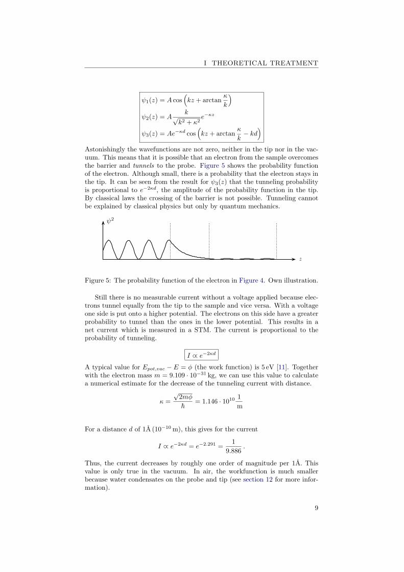
Instead of using a prototype board, which would be a simpler approach, wedecided to design a proper printed circuit board to host our components. Thesoftware used is part of the P-Cad 2006 Suite, provided by the Paul ScherrerInstitute.
Our PCB consists of four layers: two signal layers (Top and Bottom), AGND,the analog ground layer and ‘−15V’ – a power layer. It needs to be noted thatboth the AGND and the −15V layers include alterations – the AGND layer issplit up into analog and digital ground and contains a +15V and a +5V powerline. The power layer consists of the −15V and ±24V power planes.
The design of printed circuit boards generally consists of two tasks - theplacing of the components onto the board and the routing of the connections
19
II DOCUMENTATION
between the single components. To begin placing components, a netlist mustbe generated. The netlist contains the information on the components it drawsfrom the schematic. This information consists of the component’s name, con-nections and the PCB pattern - its real-life dimensions and pin designators.When generating a netlist, an automatic error check takes place, ensuring theconformity of the design to electric rules, such as checking for possible shortcircuits.
When placing components, it is best to avoid the entanglement of unroutedconnections - this contributes to the overall simplicity of the design and helpsto prevent unnecessary routing problems. To route the connections, a varietyof autorouters may be used, in our case we chose SPECCTRA, one of the moresophisticated autorouters available. It is also possible to route the connectionsby hand, however this requires a lot of time and skill. Nowadays, manual routingis mostly used for small alterations and improvements to the automatic routing.While working with our board, it was necessary for adjustment of vias and looseconnections - connections which the autorouter failed to route.
Figure 15: P-CAD 2006 PCB Designer. Own picture.
Figure 16: Empty Printed Circuit Board. Own picture.
20

II DOCUMENTATION
8 Difficulties
8.1 Vibration Damping
Section 5 concludes that the need for vibration damping depends on how rigidthe design of the STM is. The big size of our STM is a disadvantage concerningrigidity, so we required an effective damping. Our first approach consisted of theaforementioned air-filled tire and heavy metal plate but further experimentationdeemed this solution to be too sensitive to vibration. We therefore decided totake a different approach using elastic strings (Figure 17). This build seemedmore efficient than the other, though further improvements had to be done.When hanging the heavy metal plate from elastic strings, the proportions ofthe stand proved to be a determining factor. Using a ladder (Figure 17a), thefeet are too close to each other, allowing for the whole build to swing sideways.With wooden stands (Figure 17b), the feet are further apart, stabilizing the mi-croscope a lot more. The influence of outside oscillation was sufficiently reducedsuch that the tunneling current would not be strongly influenced. The elasticstrings used are actually designed for body fitness training and elongate a lot,but using multiple strings for every corner eliminated this problem altogether.As a backup for when one of the strings would tear apart, a solid cardboard boxjust centimeters beneath the hanging plate was used. The length of the stringsseemed unimportant but both external advice and our experimentation showedthat they needed to be loaded to their limit. This makes the strings harder andless prone to change their length when more or less force is applied.
(a) Hanging from a ladder. (b) Hanging from wooden stands.
Figure 17: The ladder was only a provisional, less effective stand which we laterreplaced by more stable ones. Own pictures.
8.2 Acoustic Noise
Acoustic noise negatively influenced the stability of the tunneling current whichis also related to the big size of the STM. Following an expert’s advice, we builta box lined with cone foam. However, when applied, the tunneling current wasstill very sensitive to acoustic noise. Our only temporary solution to it was toget the environment of the microscope to be as quiet as possible. The designof a new box using glass wool and aluminium foil improved noise cancellation a
21

II DOCUMENTATION
lot, so much in fact that quiet speaking around the microscope during experi-mentation did not negatively influence a measurement. The noise cancellationbox introduced another difficulty in handling though, as putting it over themicroscope after successful approaching of the tip to the sample often ruinedthe approach. It either crushed the tip into the sample or distanced the tip sofar that there was no tunneling current measurable anymore. Yet very carefulhandling of the box and microscope allowed for some successful experiments,which in turn were a lot more stable.
Figure 18: Sound isolation box. Own picture.
8.3 Tunneling Current Amplifier
In experiment, the amplifier turned out to be too slow and noise was on a criticallevel even though we had put the amplifier into a metal case to shield it. Weconducted tests with a 10 GΩ resistor and in situ with the microscope. When weremoved some capacitors to increase the speed, the noise became unacceptablyhigh. Since we could not locate a problem in the circuit, we decided to build anew amplifier.
We also had to construct a provisional case for the new amplifier, allowingus to test it. It performed well even though it was by far not as elaborate asthe first amplifier. After this success, we built a more durable case and a thirdimproved amplifier. The case was manufactured by us from a stock box of thatsize, adding the connectors and soldering the cabling inside. It features a VGAplug to connect it to the control electronics. Furthermore, there is a plug forthe piezos which is internally wired to the VGA connector. The amplifier itselfwas soldered from the individual parts on a test board and set into the boxafterwards. As an improvement from the second amplifier, we added capacitorsat the power supply lines to filter noise from the supply. Figure 20 shows theschematic of the amplifier circuit.
The acquisition of the low-noise opamps was surprisingly uncomplicated.The first amplifier used an OPA 111, the second an OPA 129 and the third onean OPA 124, all of them produced by Burr Brown, Texas Instruments. From thedata sheets one can easily tell whether an amplifier is suited for an application.Furthermore, there are sample applications on most data sheets. It is good toknow that free samples of most opamps can be ordered.
22

II DOCUMENTATION
Figure 19: The second and the third amplifier, which could be directly mountedonto the STM. Own pictures.
Figure 20: Schematic of the third amplifier. Own picture.
8.4 Control Electronics
We have encountered several problems in the course of designing the board.Since P-Cad has been discontinued, the component libraries are not updatedanymore, resulting in a lack of information concerning some of the components.To solve this, we needed to draw some of the components ourselves, as someof the patterns were nowhere to be found. Especially the female part of the120-pin I/O connector of the PIC32 board proved to be a challenge. Anotherproblem had to do with the routing - due to the somewhat wrong placementof the components, some of the power lines were barely reachable for othercomponents and therefore had to be readjusted. Further difficulty arose whenour board was rejected by Eurocircuits because of the insufficient diameter ofthe vias - connection channels from one layer to the other. This required furthercustomization of the autorouted connections from our side. After resizing thevias and refitting some of the components, the problem was solved.
23

II DOCUMENTATION
9 Current Design
After all the manipulations done by us in the course of improving the scanningresults, the following design is currently giving us the best results so far.
Figure 21: A picture showing the complete design. Own picture.
Damping is now dealt with by elastic ropes and the heavy metal plate, andmost of the noise-related problems vanished after the production and usage ofthe new, improved noise cancellation box. Some trouble still exists, though. Themain problem is the vibration caused by us putting the box over the microscopeafter the coarse approach. This could be solved by using a remotely controlledstepping motor for the coarse approach. This would allow for the box to beput over the microscope before the coarse approach – the coarse approach to bebegun only after all vibration has seized.
The latest amplifier works well with relatively little noise. The direct mountonto the STM body and the different connectors simplify the usage. There isonly one cable connecting the STM to other devices – now oscilloscopes andpower supplies, later the microcontroller interface.
In terms of control electronics, we have successfully produced a uniformcontrol box containing the hand-soldered printed circuit board, the voltage reg-ulators and power supply. Currently, the board is calibrated and the commu-nication between the processor and the DAC and ADC channels is enabled,theoretically allowing us to perform scans.
Figure 22: The control electronics in the opened box. Own picture.
24

II DOCUMENTATION
10 Future plans
10.1 Mechanical Build
The mechanical build still incorporates certain faults which we are in the courseof improving. The inclusion of a stepping motor and linked to this the changeof the form factor to a smaller lever is in conception, and a floor board for thenoise cancellation box to further enhance its effect is in production.
10.2 Control Electronics
From the present standpoint, we have fully accomplished the task of producingthe hardware necessary for the scanning of the sample. To be able to actuallygenerate the scans, the following software must be developed:
• A VISA-compliant USB Class for the communication between LabVIEWand our microprocessor and thus the transfer and processing of raw datacoming from our board
• An algorithm managing the scanning signals and reading the data comingfrom the A/D converter
• A LabVIEW Virtual Instrument which would allow us to process the dataand display the scan
Due to the complexity of the USB protocol, it has been proposed that Valerywould take over the development of the USB class, allowing us to concentrateon the other two programming tasks.
25
III EXPERIMENTAL RESULTS
Part III
Experimental Results
11 Methods
The first experiments were supposed to ensure the working of the amplifier. Weconnected an adjustable power supply and a 10 GΩ resistance in series to the twoinputs. The corresponding output voltages for the input voltage could be readout with a voltage meter or an oscilloscope. As mentioned above, we noticedthat the amplifier performed insufficiently for our purpose. Nevertheless, weused it in our first attempts to measure the tunneling current.
The experimental setup for the experiments with the STM incorporatedthe following: the mechanical body of the STM, a battery to provide a stablebias voltage, the amplifier and two power supplies – one to power the amplifierand one to control the z-piezo. We used a Highly Ordered Pyrolytic Graphite(HOPG) sample and a piece of platinum-iridium wire as the tip, which we hadboth received from Dr. Thomas Jung (PSI, Uni Basel). Already in the first fewattempts, we succeeded in detecting the tunneling current. However, the signalwas too unstable to examine its properties.
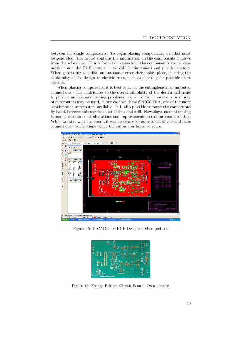
After we had made the improvements mentioned in the documentation, wefinally managed to get a rather stable signal. Computer connectible voltageprobes and the software Logger Pro immensely simplified the measurements.The probes could be borrowed from our school, however, they had a range fromonly −10 V to +10 V. This seemed sufficient for the amplifier output which hasa maximum output voltage of about 14 V. In contrast, the voltage at the z-piezoranged from 0 V to 32 V. A simple voltage divider built from a potentiometersolved the problem, dividing the voltage by four. This could be reversed onsoftware basis in Logger Pro.
Figure 23: Computer-based measurement turned out to be very helpful – ascreenshot of Logger Pro. Own picture.
26

III EXPERIMENTAL RESULTS
12 Results
Figure 24 shows two graphs we obtained from a very good measurement. Inthe lower graph, the output voltage is logarithmized, very well illustrating theexponential relationship between tunneling current and distance.
Figure 24: The two images show the results of one of our best measurements.The upper graph plots the output voltage over the voltage at the piezo (bothin Volts) – in the lower one the output voltage is logarithmized. Own pictures.
27
III EXPERIMENTAL RESULTS
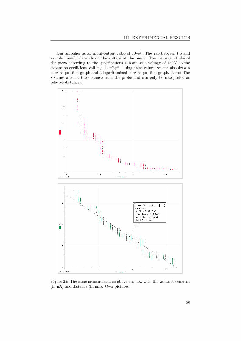
Our amplifier as an input-output ratio of 10 nAV . The gap between tip and
sample linearly depends on the voltage at the piezo. The maximal stroke ofthe piezo according to the specifications is 5µm at a voltage of 150 V so theexpansion coefficient, call it ρ, is 100 nm
3 V . Using these values, we can also draw acurrent-position graph and a logarithmized current-position graph. Note: Thez-values are not the distance from the probe and can only be interpreted asrelative distances.
Figure 25: The same measurement as above but now with the values for current(in nA) and distance (in nm). Own pictures.
28

III EXPERIMENTAL RESULTS
In section 2, we showed that the tunneling current I is proportional to e−2κd,with κ =
√2meφ
~ = 1.087 · 1010 1m . One receives this numerical value with a
workfunction equal to 4.5 eV, which is the approximate value for HOPG. We canuse the slope in Figure 25 to check correlation between theory and experiment.
Iout = I0 e−2κd
ln I = ln I0 − 2κdd lnId d
= −2κ
This means the slope in the lower graph in Figure 25 should be equal to −2κ =2.17 ·1010 1
m = 21.7 1nm . This is much greater than the measured value, by about
a factor 200. With the same values, a work function φ = 1 · 10−4 eV can becalculated. This is four orders of magnitude smaller than the actual value. Theslope was between about 0.06 1
nm and 0.18 1nm in our measurements.
As our results are reproducable, we had to find explanation for such a bigdiscrepancy. After asking him for help, Dr. Thomas Jung from PSI gave usthe hint that when operating in air, water will condensate on the sample. Thisseverly influences the work function of the material. From [5]:
Tunneling microscopy had long since entered the scientific arsenalas a precision instrument for the exploration of nanostructure of thesurface of conducting materials. At the same time, the twenty-yearexperience of using scanning tunneling microscopes (STM) has un-equivocally demonstrated that, when operating in air (ex situ) orin solutions (in situ), the behavior of the STM gap is impossibleto describe by relationships intended for the electron tunneling ina vacuum. For example, the height of the tunneling barrier, whenformally evaluated from the data of the tunneling-spectroscopy mea-surements in air with formulas for a vacuum tunneling gap is a feworders of magnitude as low as that obtained when performing mea-surements in a vacuum. At the same time, the resolution reached byan STM operating in air falls as a rule far short of that in a vacuumor even in solutions.
Specifics of the ex situ operation of STM is defined by the formationof a thin layer of condensed moisture in the gap. The layer is in factan electrolyte of an indefinite composition. The condensate on thesurface was in some cases observed experimentally. When movedin, the STM tip is as a rule immersed into such a layer and thegap current has an electrochemical origin. As a result, at the samespecified values of current, the tip-sample distance in the ex situSTM configuration happens to be far greater than in vacuum (orlow-temperature) STM.
Drawing from the source, we can deduce that the big discrepancy betweentheory and experiment is due to the humid environment whereas the differentvalues of the measured slopes can be attributed to an error in measurement.This is rather obvious, considering that even the graph of good measurementsis rather a bar than a line and that external influences are still noticeable.
Sudden jumps of the current posed a frequent problem (Figure 26). Con-cluding from the quotation above, it seems probable that the tip moves into the
29

III EXPERIMENTAL RESULTS
condensate when the current jumps. Forces between the tip and the sample canalso contribute to this problems. It is known that the attractive force betweenthe tip and a HOPG sample can deform the sample [3].
Figure 26: The tunneling current remains almost constant until it makes asudden jump. Own picture.
30

CONCLUSION
ConclusionIn the course of the past six months, we have been investing major portions ofour time for this, many would say, daring project of building such a device. Ithas involved a lot of hard work, patience and a lot of help from all sides. It hasalso taken a great deal of organisational work to pull this through. But we havehad a great time, trying to master this challenge we have set before us. It hasbeen fascinating to be able to create such an instrument and a great opportunityto immerse ourselves in this area of physics, closely related to nanotechnology,a topic which is on everyone’s lips nowadays. We have discovered what it’s liketo be engaged in a scientific pursuit and how captivating such research can be.A further interesting aspect of our work was the development of solutions to thevarious problems, which inevitably arise in the course of such a large project.
Despite the fact that we did not succeed in accomplishing the fully functionalmicroscope as we initially hoped to, we do not plan on giving up this projectand it is our wish and ambition to continue working in the same direction andachieve the goal we have set before us.
31

REFERENCES
References
[1] Chen, C. Julian. 1993.Introduction to Scanning Tunneling Microscopy.Oxford University Press. New York.
[2] Jia, Jin-Feng; Yang, Wei-Sheng and Xue, Qi-Kun.Scanning Tunneling Microscopy.In: Yao, Nan and Wang, Zhong Lin (Publ.). Handbook of Microscopy forNanotechnology.Kluwer Academic Publisher. New York.
[3] Kusunoki, Kouji; Sakata, Ichiro; Miyamura, Kazuo.Interaction between Tip and HOPG Surface Studied by STS.In: Analytical Sciences 2001, Vol.17 Supplement, i1267-i1268.
[4] Park, Sang-il and Barrett, Robert C. (1993).Design Considerations for An STM System.In: Stroscio, Joseph A. and Kaiser, William J. (Publ.). Scanning TunnelingMicroscopy.Academic Press, Inc. San Diego.
[5] Yusipovich, A. I.; Vassiliev S. Yu.Voltage–Height Spectroscopy in the Ex Situ Configuration of a Scanning Tun-neling Microscope.In: Russian Journal of Electrochemistry, Vol. 41, No. 5, 2005, pp. 510–521.
[6] Jurgen MullerAn Amateur Scanning Tunneling Microscope.http://www.e-basteln.de/ (January 8, 2009)
[7] Piezoelectricity.http://en.wikipedia.org/wiki/Piezoelectricity (January 8, 2009)
[8] Piezomechanik GmbH.http://www.piezomechanik.com (January 8, 2009)
[9] Dreyer, Hans Peter; Brovelli, D.; Cornaz, A.;Dunki, R.; Lohe, H.-J.Raster-Tunnel-Mikroskop (Leitprogramm).http://www.educ.ethz.ch/lehrpersonen/physik/unterrichtsmaterialien_
phy/modernephysik/raster_tunnel/index (January 8, 2009)
[10] SXM Project.http://sxm4.uni-muenster.de/stm-de (January 8, 2009)
[11] Work function.http://en.wikipedia.org/wiki/Work_function (January 8, 2009)
32