Digital Logic Design Lecture # 9 University of Tehran.
26
Digital Logic Design Lecture # 9 University of Tehran
-
Upload
dora-dixon -
Category
Documents
-
view
220 -
download
0
Transcript of Digital Logic Design Lecture # 9 University of Tehran.

Digital Logic Design
Lecture # 9University of Tehran

Outline
MSI Parts as a Decoder Multiplexer Three State Buffer MSI Parts as a Multiplexer Realization of Switching Functions
Using Multiplexers

MSI Parts as a Decoder Up till now, we saw a modular component
named as a decoder. Let’s now see what standard modules with that functionality are available.
74138: This standard decoder is the most used in between the MSI decoders. It has active-low outputs, and one of the enable inputs is also active-low, while the other two are active-high. There is no particular reason to why they are 3 enable inputs other than obeying the standard number of pins these packages have.
1
Y 0 N
Y 1 N
Y 2 N
Y 3 N
Y 4 N
A
B
C
G 1
Y 5 N
Y 6 N
Y 7 N
G 2 A N
G 2 B N
7 4 1 3 8
3 :8 D E C O D E R
MSI Parts as a Decoder (continued…) 74154: As in the 74138, this package also
needs activity of both enable pins to work.2
O 0 N
D
C
B
A
G 2 N
G 1 N
O 1 2 N
O 11 N
O 1 0 N
O 1 5 N
O 1 4 N
O 1 3 N
O 1 N
O 2 N
O 3 N
O 4 N
O 5 N
O 6 N
O 7 N
O 8 N
O 9 N
7 4 1 5 4
D E C O D E R

MSI Parts as a Decoder (continued…) 74139: This decoder is often called a dual 2-to-
4 decoder and is actually just two 2-to-4 decoders in one chip.
3
A 1B 1A 2B 2G 1 NG 2 N
Y 1 0 N
Y 2 0 NY 1 3 NY 1 2 NY 11 N
Y 2 3 NY 2 2 NY 2 1 N
7 4 1 3 9
2 :4 D E C O D E R

Multiplexer Data is stored as bytes in computer memory.
When discussing data transport, a lot of wiring would be needed to be able to move 8 bits of a byte in parallel. Trading cost for performance we use serial connections to transport one bit of data at a time. This means we share a transition line between the source and destination.

Multiplexer (continued…) For instance, in the following diagram, the
transition line works of 1ms between A and A’ and then changes position as the next bit move on. In this diagram the first box is a multiplexer and the second a demultiplexer. The multiplexers we discuss have no memory.
A
DCB
A’
D’C’B’
Multiplexer Demultiplexer

Multiplexer (continued…) Let us consider such a module with one output
and four inputs, where one of the four inputs must be selected for output through 2 selection lines.
I0I1I2I3
S0S1
y
MUXy
0
0
00
1
1 1
1
S0S1
I0
I1
I2
I3

Multiplexer (continued…) To observe the gate level design of such
structures, let’s consider a dual 4-to-1 MUX and show its design:
1I0
2I0
2I1
2I2
2I3
2y
2en
1I1
1I2
1I3
1y
1en
S0S1
1I01I11I21I3
1y
1en
2I02I12I22I3
2y
2en
S0
S1 }0/3

Multiplexer (continued…) We need to be able to construct larger
multiplexer modules by cascading smaller ones. This cascading is done by using the enable inputs of our smaller modules as shown in the following figure:
1I01I11I21I3
1y
1en
2I02I12I22I3
2y
2en
S0
S1 }0/3
S0S1S2
abcd
efgh
y

Multiplexer (continued…) Recall the structure can be used as
a 1-to-2 decoder which has been used to choose the particular 4-to-1 MUX to be enabled in the last example. That is when s2=0 the upper package is working and when s2=1 the lower one. We could have used a 2-to-1 MUX to choose between 1y and 2y and use s2 as the selector.
y0
y1

Multiplexer (continued…) Let’s observe different structures of a 2-to-1
MUX:
I0
I1
y
64
64
64
s
1
I0
I1
y
s
2

Multiplexer (continued…) About the second structure as a MUX shown in
the last slide it must be mentioned that it would have been logically correct use a PMOS transistor instead of the inverter and NMOS, but PMOS transistors are much slower than the same size NMOS transistors, so this structure is preferred (this structure uses the level before as its power supply).

Multiplexer (continued…) Multiplexers can be used in the design of both
complex circuits and also realization of primitive gates such as XOR and AND gates.
XOR gate: If we look at an XOR gate’s functionality a little differently, we can easily see that when one input is 0 the other is simply propagated through and when one is 1 the other is complemented. Using a multiplexer to realize this, is shown in the following figure. This realization uses only 6 transistors if we use the second method used for a 2-to-1 MUX whereas XOR gates usually consist of 8 transistors.a b y
0
1
1
0
0
00
1
1 1
1
0
a
b
b-
y0
1

Multiplexer (continued…) AND gate: Again we use only 4 transistors instead of
the usual 6 used for an AND gate.
a b y
1
0
0
0
0
00
1
1 1
1
0
a
0
b
y0
1

Three State Buffer Another useful and primitive component in
digital circuits is the three state buffer:
This three state buffer lets it’s input through to the output when the control is 1 and give a high impedance output otherwise.
c a y
1
0
Z
0
0
00
1
1 1
1
Z
ENB
a(input)
c(control)
y(output)
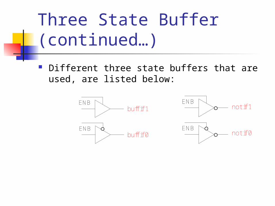
Three State Buffer (continued…) Different three state buffers that are used, are
listed below:
ENB
ENB
buff if 1
buff if 0
ENB
ENB
not if 1
not if 0

Three State Buffer (continued…) Let us know use our knowledge of three state
buffers to construct other structures that realize multiplexers and observe some new concepts. Thus for a 4-to-1 MUX, we have:
y0
y1
y2
y3
en
1 0
ENB
ENB
ENB
ENB
I0
I1
I2
I3

Three State Buffer (continued…) Note: It must be taken to consideration that a
wired OR structure can only be used when we have three state lines.
We can do cascading on packages with three state outputs with the same type of ORing:
I0I1I2I3
y
en
S0S1S2
I0I1I2I3
y
enabcd
hgfe
S0
S0
S1
S1
Shows threestate outputs

MSI Parts as a Multiplexer Let us now see some standard multiplexer
packages. 74153: It’s clear that this package is a dual 4-
to-1 multiplexer.1
2 Y
1 Y
1 C 1
1 C 0
1 G N
2 C 0
2 G N
1 C 3
1 C 2
2 C 2
2 C 1
A
B
2 C 3
7 4 1 5 3
M U LT IP L E X E R
MSI Parts as a Multiplexer (continued…) 74157: This is a quad 2-to-1 MUX with
common select and enable inputs. Outputs are not in three state.
2
A 1
B 1
S E L
B 2
A 3
B 3
A 2
B 4
G N
A 4
Y 1
Y 2
Y 3
Y 4
7 4 1 5 7
M U LT IP L E X E R

MSI Parts as a Multiplexer (continued…) 74251: This is an 8-to-1 MUX that gives us the
complemented form of the output too. The outputs are three state and the last level of the MUX can be seen below:
3
G N
D 3D 2D 1D 0
D 7D 6D 5D 4
CBA
Y
W N
M U LT IP L E X E R
7 4 2 5 1
ENBy
WN
...

MSI Parts as a Multiplexer (continued…) Note:
ENB

Realization of Switching Functions Using Multiplexers Multiplexers can also be used to realize more
complex switching functions, for example we will now realize a full adder using a 74153 multiplexer module.
F . A.
a b
cin cout
sum
a b cin co
0
0
00
00
000 0
0
0
0
1
0
1
11
1
11
0
1
0
111
11
1
1
1
S
0
0
11
1
1
0
0

Realization of Switching Functions Using Multiplexers (continued…)
20 1
1 0
ab
cin00
0
1
0
1 3
40 1
1 0
6
7 5
01 11 10
Scin cincin cin
4
0 11
06
7 5
20
1
10
ab
cin00
0
1
0
1 3
01 11 10
co0 1cin cin

Realization of Switching Functions Using Multiplexers (continued…)
0123
en
0123
en
10 }0/3
ab
S
cin
cin
co
0
1
cin