Design of Ultra-Low Power Circuits for Battery-Powered ... · PDF fileDesign of Ultra-Low...
14
1 SNAA301A – January 2017 – Revised May 2017 Submit Documentation Feedback Copyright © 2017, Texas Instruments Incorporated Design of Ultra-Low Power Circuits for Battery-Powered Wireless PIR Motion Detectors Application Report SNAA301A – January 2017 – Revised May 2017 Design of Ultra-Low Power Discrete Signal Conditioning Circuit for Battery-Powered Wireless PIR Motion Detectors Bahram Mirshab ABSTRACT In this document, a cost-optimized, ultra-low power op amp interface for wireless battery operated PIR (Passive Infrared) motion detectors is described. A single new 4-channel nanopower operational amplifier, TLV8544, implements the analog signal path, including two gain stages, two bandpass filters, and a window comparator. Contents 1 Introduction ................................................................................................................... 2 2 Passive Infrared (PIR) Motion Detector Sensor ......................................................................... 2 3 Biasing PIR Sensor for Low Power Operation ........................................................................... 4 4 Gain Stages and Band Pass Filtering .................................................................................... 4 5 Calculation Of The Total Gain Of Stages “A” AND “B” ................................................................. 7 6 Window Comparator Stage ................................................................................................. 7 7 Current Consumption ...................................................................................................... 11 8 Conclusion .................................................................................................................. 11 9 Device Family ............................................................................................................... 12 10 References .................................................................................................................. 12 List of Figures 1 Block Diagram of a Wireless Battery Operated PIR Motion Detector System....................................... 2 2 (a) PIR Senor, (b) PIR Transducer, (c) PIR Sensor Output In Presence of Motion of a Heat Source In The Field Of View............................................................................................................ 3 3 Murata Surface Mount PIR Sensor and Fresnel Lens Used in the Design .......................................... 3 4 PIR Sensor Biasing Method for Low Power Consumption ............................................................. 4 5 The Analog Stages For Filtering and Amplifying the Sensor Signal .................................................. 5 6 Input Stage “A” Bandpass Filter, Gain and Clamp ...................................................................... 6 7 Stage “B”; Bandpass Filter And Gain .................................................................................... 7 8 Amplified PIR Signal and The Output Signals of The Window Comparator Circuit ................................. 8 9 The Window Comparator Circuit Made of Amplifier "C" And "D" of TLV8544 ....................................... 9 10 Adding Hysteresis To The Inverting Comparator ...................................................................... 10 11 Adding Hysteresis To The Noninverting Comparator ................................................................. 11 12 PIR Motion Detector Experiment Board, BOOSTXL-TLV8544PIR ................................................. 12
Transcript of Design of Ultra-Low Power Circuits for Battery-Powered ... · PDF fileDesign of Ultra-Low...
1SNAA301A–January 2017–Revised May 2017Submit Documentation Feedback
Copyright © 2017, Texas Instruments Incorporated
Design of Ultra-Low Power Circuits for Battery-Powered Wireless PIR MotionDetectors
Application ReportSNAA301A–January 2017–Revised May 2017
Design of Ultra-Low Power Discrete Signal ConditioningCircuit for Battery-Powered Wireless PIR Motion Detectors
BahramMirshab
ABSTRACTIn this document, a cost-optimized, ultra-low power op amp interface for wireless battery operated PIR(Passive Infrared) motion detectors is described. A single new 4-channel nanopower operational amplifier,TLV8544, implements the analog signal path, including two gain stages, two bandpass filters, and awindow comparator.
Contents1 Introduction ................................................................................................................... 22 Passive Infrared (PIR) Motion Detector Sensor ......................................................................... 23 Biasing PIR Sensor for Low Power Operation ........................................................................... 44 Gain Stages and Band Pass Filtering .................................................................................... 45 Calculation Of The Total Gain Of Stages “A” AND “B” ................................................................. 76 Window Comparator Stage................................................................................................. 77 Current Consumption ...................................................................................................... 118 Conclusion .................................................................................................................. 119 Device Family............................................................................................................... 1210 References .................................................................................................................. 12
List of Figures
1 Block Diagram of a Wireless Battery Operated PIR Motion Detector System....................................... 22 (a) PIR Senor, (b) PIR Transducer, (c) PIR Sensor Output In Presence of Motion of a Heat Source In
The Field Of View............................................................................................................ 33 Murata Surface Mount PIR Sensor and Fresnel Lens Used in the Design .......................................... 34 PIR Sensor Biasing Method for Low Power Consumption ............................................................. 45 The Analog Stages For Filtering and Amplifying the Sensor Signal .................................................. 56 Input Stage “A” Bandpass Filter, Gain and Clamp ...................................................................... 67 Stage “B”; Bandpass Filter And Gain .................................................................................... 78 Amplified PIR Signal and The Output Signals of The Window Comparator Circuit................................. 89 The Window Comparator Circuit Made of Amplifier "C" And "D" of TLV8544 ....................................... 910 Adding Hysteresis To The Inverting Comparator ...................................................................... 1011 Adding Hysteresis To The Noninverting Comparator ................................................................. 1112 PIR Motion Detector Experiment Board, BOOSTXL-TLV8544PIR ................................................. 12

Gain, bandpass filter & clamp
Window comparator
SimpleLink multi-standard 2.4 GHz
(ARM M3)
PIR Sensor
Rg
D
S
CR2032 coin cell battery
TLV8544 C & D
TLV8544 A & B
CC2650
Mot
ion
x
Copyright © 2017, Texas Instruments Incorporated
Supply Voltage
TLV8544
Introduction www.ti.com
2 SNAA301A–January 2017–Revised May 2017Submit Documentation Feedback
Copyright © 2017, Texas Instruments Incorporated
Design of Ultra-Low Power Circuits for Battery-Powered Wireless PIR MotionDetectors
1 IntroductionSmart building automation systems employ a large number of various sensing nodes distributedthroughout small, medium and large infrastructures. The sensing nodes measure motion, temperature,vibration, and other parameters of interest. Wireless nodes are monitored in a central location. Because ofthe large number of distributed nodes possible in such a system, battery operated nodes designed withcost-effective, nanopower, electronic components are desirable. Typically, the wireless nodes need to runon a single CR2032 coin battery for eight to ten years. The block diagram of a wireless, battery-poweredPassive Infrared (PIR) motion detector is shown in Figure 1. Such detectors are widely used in industrial,commercial and residential building automation applications—See TI reference design, TIDA-01398, formore system information.
Figure 1. Block Diagram of a Wireless Battery Operated PIR Motion Detector System
In this document, an analog interface circuit for a PIR motion detector, suitable for smart buildingautomation applications, is described. The TLV8544, a new 4-channel nanopower amplifier designed forcost-sensitive systems, is utilized to reduce the power consumption of the sensor node. Configuring twoamplifiers of the quad operational amplifier package for amplifying/filtering the signal, and the remainingtwo amplifiers for implementing a window comparator cost effectively. A booster board, BOOSTXL-TLV8544PIR, for CC2650 Launchpad LAUNCHXL-CC2650 is available from TI website for hands-onexperimentation and evaluation of the PIR motion detector circuit.
2 Passive Infrared (PIR) Motion Detector SensorThe pyroelectric material used in a PIR sensor generates an electric charge when subjected to thermalenergy flow through its body [1]. The phenomenon is actually a secondary effect of thermal expansion ofthe pyroelectrics material, which is also piezoelectric. The absorbed heat by the material causes the frontside of the sensing element to expand. The resulting thermally induced stress leads to presence of apiezoelectric charge on the element electrodes. This charge shows up as voltage across the electrodesdeposited on the opposite sides of the elements.
Due to the piezoelectric properties of the element, if the sensor is subjected to a slight mechanical stressby any external force, it generates a charge indistinguishable from that caused by the infrared heat waves.For this reason, the PIR sensors are fabricated symmetrically, as shown in Figure 2(b), by placingidentical elements inside the sensor’s package. The elements are connected to the electronic circuit in away to produce out-of-phase signals when subjected to the same in-phase inputs. Hence, spurious heat(or external force) signals applied to both electrodes simultaneously (in phase) will be canceled at theinput of the circuit, whereas the variable thermal radiation due to motion of a heat source to be detectedwill be absorbed by only one element at a time, avoiding cancellation. A JFET transistor is used as avoltage buffer and provides a DC offset at the sensor output.

Murata IML-0669 Fresnel Lens for SMD type PIR
Murata IRS-B210ST01-R1 Surface mount Pyroelectric, Motion
Sensing SMD Module
(a) (b)
VBAT
PIR element
RgR
D
S
VOUT
xxxxxxxxx
xxxxxxxxxx
xx+
-
+
-
Mot
ion
Vbias
Upper Electrode
x
(a)
(b)
(c)
Bottom electrodes
Rg
GND
D
S
Vout
VCC
Bottom electrodes
To Rg resistor
C1
C2
+ -
+ -
R
Circuit representation of PIR sensor(d)
www.ti.com Passive Infrared (PIR) Motion Detector Sensor
3SNAA301A–January 2017–Revised May 2017Submit Documentation Feedback
Copyright © 2017, Texas Instruments Incorporated
Design of Ultra-Low Power Circuits for Battery-Powered Wireless PIR MotionDetectors
Figure 2. (a) PIR Senor, (b) PIR Transducer, (c) PIR Sensor Output In Presence of Motion of a HeatSource In The Field Of View
The output voltage signal due to a moving object in the sensor’s field of view is shown in Figure 2(c). Theamplitude of this signal is proportional to the speed and distance of the object relative to the sensor and isin a range of a few hundred microvolts Vp-p up to low millivolts Vp-p. The best sensor response isachieved if it is physically mounded on the board such that the motions are across the elements. Noticethat the sensor detects the heat emitted from a source relative to the ambient temperature surrounding thesource, therefore, the sensor in the system should be placed away from other sources of time varying highheat such as discharge vents and lamps.
A Murata surface mound (SMD) type PIR sensor [2] and the related lens [3] used in this design is shownin Figure 3. The Fresnel lens is needed in front of the PIR sensor to extend the range of the sensor in adesired field of view. The lens focuses the IR energy onto the small sensor elements in the sensor.Depending on each application, the lens is design for a particular overall viewing angle and detection areacoverage.
Figure 3. Murata Surface Mount PIR Sensor and Fresnel Lens Used in the Design

3.3 V
PIR
R1
R2
To the gain/bandpass filter stages
C1
Rg
D
S
Large resistor value to lower current
consumption
Rad
iate
d he
at fr
om
an o
bjec
t in
mot
ion
x
Signal caused by the motion of an object in the field of view
Murata IML-0669 Fresnel Lens for SMD
type PIR
Murata IRS-B210ST01-R1 Surface mount
Pyroelectric, Motion Sensing SMD Module
Supply line filter
DC biasresistor
Biasing PIR Sensor for Low Power Operation www.ti.com
4 SNAA301A–January 2017–Revised May 2017Submit Documentation Feedback
Copyright © 2017, Texas Instruments Incorporated
Design of Ultra-Low Power Circuits for Battery-Powered Wireless PIR MotionDetectors
The micropower circuit around the PIR sensor typically takes up to 30 seconds to charge all thebypass/feedback capacitors through all the large value resistors. During this time the signal from the laststage is not stable. Therefore, power cycling of the PIR senor and the related analog interface is notpractical in motion detection application and the sensor and the interface must be kept "on" continuously.
The bypass capacitor C1 is a critical component because the power supply rejection ratio (PSRR) of thedetector is poor (less than 10 dB). Any fluctuation of the supply due to noise will be seen as a signal bythe gain stages, resulting in false triggering at the output.
3 Biasing PIR Sensor for Low Power OperationThe PIR sensor supply range is from 2 V to 15 V, in this case about 3V, directly supplied from the battery.As mentioned in the previous section, it must stay on continuously in the system due to its long warm uptime from off condition.
Figure 4. PIR Sensor Biasing Method for Low Power Consumption
As shown in Figure 4, the current through the JFET output transistor of the PIR sensor is controlled byresistor R2, which also, provides the DC bias for the first amplifier stage. Since power cycling of the PIRsensor is not practical, to reduce the current consumption of the sensor substantially, a much larger value(1.3 MΩ) of R2 than the recommended value (47 kΩ) by the sensor manufacturer is used. The penalty isdecreased sensitivity and higher output noise at the sensor output, which is a fair tradeoff for increasedbattery lifetime. To compensate the loss of sensitivity at the sensor output, higher gain value in the filterstages in necessary.
4 Gain Stages and Band Pass Filtering
4.1 Circuit DescriptionThe analog signal path is shown in Figure 5.

Vin
_
+
_
+
TLV8544BTLV8544
A
TLV8544C
TLV8544D
Window Comparator
_
_
+
+MCU I/O
MCU I/O
Gain Stages, bandpass filters
R1
C1
R3
C2
C3
R4C4
R5
C5
R6
R7
R10
C7R8
C6
C8
D1
D2
R9
RgR2
D
S
PIR
Quad Package Supply Pin
VBAT
VBAT
CR2032 coin cell
VBAT
Rad
iate
d he
at fr
om a
n ob
ject
in m
otio
n
x
Signal
VBAT
VREF generator network
IVR
EF
Fresnel Lens
www.ti.com Gain Stages and Band Pass Filtering
5SNAA301A–January 2017–Revised May 2017Submit Documentation Feedback
Copyright © 2017, Texas Instruments Incorporated
Design of Ultra-Low Power Circuits for Battery-Powered Wireless PIR MotionDetectors
Figure 5. The Analog Stages For Filtering and Amplifying the Sensor Signal
The TLV8544 quad op amp is powered directly by a 3.3 V CR2032 coin battery. The first two amplifierstages of the TLV8544 amplify and filter the signal from the PIR senor. The remaining opamps of theTLV8544 are used for making a window comparator. The comparator signals the detection of a motionevent to an ultra-low power wireless microcontroller on the board. Due to the higher gain in the filterstages and higher output noise from the sensor, it is necessary to optimize the placement of the highfrequency filter pole and the window comparator thresholds to avoid false detection.
The first two amplifiers (“A” and “B”) in the circuit are used in identical active bandpass filters with cornerfrequencies of 0.7 and 10.6 Hz. Each filter stage has a gain of about 220 V/V to account for the reducedsensitivity of the sensor due to the low current biasing of the PIR sensor. Considering the 8 kHz unity gainbandwidth (UGBW) product of the TLV8544, the bandwidth of each stage is limited to approximately 36Hz. The above choice of cutoff frequencies give a relatively wide bandwidth to detect a person running inthe field of view, yet narrow enough to limit the peak-to-peak noise at the output of the filters.
Amplifier “A” is a noninverting gain/filter stage, providing the high input impedance needed to preventloading of the sensor. The DC gain of the stage due to the presence of C6 is unity. Therefore, the sensoroutput provides the bias voltage needed at the “A” stage to avoid clipping of the lower cycle of the inputsignal. Diodes D1 and D2 limit the output signal, avoiding over-driving of the second stage, andconsequently placing a large charge on coupling capacitor C4, which helps with the recovery time.

Vin
_
+
TLV8544A
Noninverting gain/bandpass stage ³$´DQGLQSXWYROWDJHFODPS
R5 C5
R6
C6
D1
D2
From PIR Output To gain/ILOWHUVWDJH³%´
R5G 1
R6
Chigh5 5
12
¦R C
Su u
Clow6 6
12
¦R C
Su u
Gain Stages and Band Pass Filtering www.ti.com
6 SNAA301A–January 2017–Revised May 2017Submit Documentation Feedback
Copyright © 2017, Texas Instruments Incorporated
Design of Ultra-Low Power Circuits for Battery-Powered Wireless PIR MotionDetectors
4.2 Calculation of the Cutoff Frequencies and Gain Of Stage “A”:The low cutoff frequency of amplifier "A" is:
(1)
Choosing R6 = 6.81 kΩ and C6 = 33 μF, the low cutoff frequency is fClow= 0.71 Hz. The high cutofffrequency of the filter is:
(2)
For R5 = 1.5 MΩ and C5 = 0.01 µF, the high cutoff frequency is fChigh= 10.6 Hz. The gain of the stage is:
(3)
Choosing R5 = 1.5 MΩ and R6 = 6.81 kΩ, the gain of the stage “A” is G=221.26 V/V (46.9dB)
Figure 6. Input Stage “A” Bandpass Filter, Gain and Clamp
4.3 Calculation Of The Cutoff Frequencies And Gain Of Stage “B”As shown in Figure 7, amplifier “B” is an inverting bandpass filter and gain stage. Capacitor C4 creates anAC coupled path between the “A” and the “B” stages. Thus the signal level must be shifted at the input ofthe amplifier “B”. This is done by connecting a midpoint voltage of the reference voltage dividerscomprising R10, R9, R8 and R7 to the non-inverting input of amplifier “B”, biasing the input signal to themid-rail (1.65V).
Because the input impedance of the TLV8544 is very high (CMOS input), the positive terminal of theamplifier "B" provides a desired high impedance node for the voltage divider to prevent increase in staticcurrent consumption of the reference voltage generator circuit. That is the main reason for using aninverting configuration in stage "B".
A very large feedback resistor R3 is chosen to minimize the dynamic current due to presence of peak-to-peak noise voltage at the output of this stage.

R3G
R4
Chigh3 3
12
¦R C
Su u
Clow4 4
12
¦R C
Su u
Inverting gain/bandpass ILOWHUVWDJH³%´
From the gain/bandpass filter VWDJH³$´
From the center tap of the reference generator network (VCC/2 Bias)
To the inputs of the window comparator
_
+
TLV8544B
R3
C2
C3
R4C4
www.ti.com Calculation Of The Total Gain Of Stages “A” AND “B”
7SNAA301A–January 2017–Revised May 2017Submit Documentation Feedback
Copyright © 2017, Texas Instruments Incorporated
Design of Ultra-Low Power Circuits for Battery-Powered Wireless PIR MotionDetectors
Figure 7. Stage “B”; Bandpass Filter And Gain
The low cutoff frequency of amplifier "B" is:
(4)
Choosing R4 = 68.1 kΩ and C4 = 3.3 μF, the low cutoff frequency is, fClow = 0.71 Hz. The high cutofffrequency of the filter is:
(5)
For R3 = 15 MΩ and C3 = 1000 pF, the high cutoff frequency is, fChigh= 10.6 Hz. The gain of the stage is:
(6)
For R3 = 15 MΩ and R4 = 68.1 kΩ, the gain is calculated |G|=220.26 V/V (46.9 dB).
5 Calculation Of The Total Gain Of Stages “A” AND “B”The overall gain of the two stages “A” and “B” is: GTotal= GA*GB= 221.26*220.26=48810 V/V = 93.77 dB.
6 Window Comparator StageThe signal from a moving object in front of the PIR sensor, after amplification and filtering, is connected toa window comparator. The comparator converts the analog signal to digital pulses for interrupting an on-board MCU (microcontroller unit), flagging detection of motion. A different approach is to digitize theanalog signal continuously by an ADC (analog-to-digital converter) and implement the comparatorfunctionality in the digital domain. This method has the advantage of enabling the post processing of thedata to reduce the chance of false detection. However, continuous conversion and processing of data bythe MCU increases the power consumption, lowering the battery's life time drastically. Therefore, awindow comparator in this case is used to wake up the MCU from power-down state when the PIR signalbegins to change due to presence of motion in the field of view.
6.1 Making A Window Comparator With OpampsRather than using separate low power comparator integrated circuits to implement the window comparatorsection of the circuit, the remaining opamps in the TLV8544 package are used to implement thecomparator stage. Benefits of this approach include fewer components and thus reduced system cost.
Although an opamp can sometimes be used as a comparator, an amplifier cannot be used as acomparator interchangeably in all applications because of amplifiers’ relatively long recovery time fromoutput saturation and relatively long propagation delay due to internal compensation. Particularly, thenanopower opamps have very slow slew rate, limiting their usage as a comparator in only applicationswith very low frequency input signal.
Vbias
VBAT
GND
VREF_High
VREF_Low
&RPS³&´2XWSXW
&RPS³'´2XWSXW
Order of the pulses depends on the direction of the motion
PIR signal
Window Comparator Stage www.ti.com
8 SNAA301A–January 2017–Revised May 2017Submit Documentation Feedback
Copyright © 2017, Texas Instruments Incorporated
Design of Ultra-Low Power Circuits for Battery-Powered Wireless PIR MotionDetectors
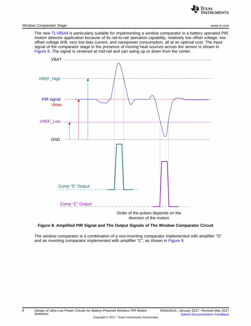
The new TLV8544 is particularly suitable for implementing a window comparator in a battery operated PIRmotion detector application because of its rail-to-rail operation capability, relatively low offset voltage, lowoffset voltage drift, very low bias current, and nanopower consumption, all at an optimal cost. The inputsignal of the comparator stage in the presence of moving heat sources across the sensor is shown inFigure 8. The signal is centered at mid-rail and can swing up or down from the center.
Figure 8. Amplified PIR Signal and The Output Signals of The Window Comparator Circuit
The window comparator is a combination of a non-inverting comparator implemented with amplifier “D”and an inverting comparator implemented with amplifier “C”, as shown in Figure 9.

_
6
REF Low CC CC CC6
R7 1.5 10V V V 0.25 V
R8 R9 R10 R7 6 10
u§ · u u¨ ¸ © ¹ u
_
6
REF High CC CC CC6
R7 R8 R9 4.5 10V V V 0.75 V
R7 R8 R9 R10 6 10
u§ · u u¨ ¸ © ¹ u
TLV8544C
TLV8544D
VBAT
Window Comparator stage implemented using the remaining two
opamps of quad TLV8544
_
_
+
+MCU I/O
MCU I/O
R7
R10
C7R8
C8
R9
7RWKHJDLQ6WDJH³%´
noninverting input (VCC/2 Bias)
)URPWKHJDLQ6WDJH³%´2XWSXW
(amplified PIR signal)
Inverting &RPS³&´
Noninverting &RPS³'´
VREF_High
VREF_Low
www.ti.com Window Comparator Stage
9SNAA301A–January 2017–Revised May 2017Submit Documentation Feedback
Copyright © 2017, Texas Instruments Incorporated
Design of Ultra-Low Power Circuits for Battery-Powered Wireless PIR MotionDetectors
Figure 9. The Window Comparator Circuit Made of Amplifier "C" And "D" of TLV8544
6.2 Reference VoltagesReferring to Figure 9, the divider networks comprising R7, R8, R9 and R10, generate the referencevoltages “VREF_High” and “VREF_Low” of the window comparator. The center point of the dividerprovides the bias voltage of the gain in the stage “B” through the connection to the noninverting input ofthe amplifier.
Due to the very low bias current of the TLV8544, it is possible to use very large values of resistors in thedivider networks to minimize the current to ground through the resistors to a negligible amount. For R7 =R8 = R9 =R10 = 15 MΩ:
(7)
(8)
Low leakage ceramic capacitors C7 and C8 maintain constant threshold voltages, preventing potentialchatter at the output of the comparators. The comparator outputs stay low in the absence of motion acrossthe sensor. In the presence of motion, comparators ”C” and “D” generate “high” output pulses as shown inFigure 8. The order of the pulses depends on the direction of the motion in front of the sensor.

LTR1
V VOLR1 R2§ ·
E u¨ ¸© ¹
UTR1
V VOHR1 R2§ ·
E u¨ ¸© ¹
_REF LowR2
VR1 R2§ ·
u¸¹
E ¨ ©
_REF LowR2 R1
V V VOR1 R2 R1 R2§ · § ·
u u¨ ¸ ¨ ¸ © ¹ © ¹
TLV8544
C_
+VO
3.3 VR1
Vin
VREF_Low
Vin
Vout
R2 VOH
VOL
Hysteresis
VLT VUT
Inverting Op-uu^_
with hysteresis
t
(a) (b)
Window Comparator Stage www.ti.com
10 SNAA301A–January 2017–Revised May 2017Submit Documentation Feedback
Copyright © 2017, Texas Instruments Incorporated
Design of Ultra-Low Power Circuits for Battery-Powered Wireless PIR MotionDetectors
6.3 Adding Hysteresis to the Window ComparatorThe window comparator of the PIR motion detector described in section does not include hysteresis. Thisis because the opamps are slow and do not react to narrow transitions on the input line rapidly, andtherefore, the circuit works well without adding hysteresis. Additionally, hysteresis would cause increasedstatic current dissipation and interference with the divider function due to the changing input impedance,and would require “uneconomical” hysteresis resistor values (100M or higher). In the event that the readerdesires to add hysteresis to the window comparator, at the expense of increased current consumption, thefollowing section describes the circuits for adding hysteresis. For a in-depth coverage of this topic pleasesee the LM139-N Datasheet and the application note SNOA654A "AN-74 LM139/LM239/LM339 A Quad ofIndependently Functioning Comparators"
6.3.1 Adding Hysteresis to the Inverting Comparator
The inverting voltage comparator circuit with external hysteresis resistors R1 and R2 is shown in (a). Thecorresponding voltage characteristic is shown in Figure 10(b).
Figure 10. Adding Hysteresis To The Inverting Comparator
The voltage at the noninverting input is [4]:
(9)
The amount β that the transition voltage is shifted is given by:
(10)
The upper transition voltage VUT, and the lower transition voltage VLT are given by:
(11)
(12)
6.3.2 Adding Hysteresis to the Noninverting ComparatorThe noninverting comparator circuit external hysteresis resistors R1 and R2 are shown in Figure 11(a).The corresponding voltage characteristic is shown in Figure 11(b).

ITotal = 0.5A + A+ 1.6A = 2.16 A
9QTLVI 4 400 10 1.6 A
u u P
IVREF = 3.3 V
4Û156À A
LTR1
V VOHR2§ ·
D u¨ ¸© ¹
UTR1
V VOLR2§ ·
D u¨ ¸© ¹
_REF HighR1
1 VR2
§ · u¨ ¸© ¹
v
TLV8544D_
+VO
Vin
VREF_High
3.3 VR1
R2
Vin
VO
VOL
Hysteresis
VLT VUT
VOH
Noninverting Op-amp Comp ³'´ZLWKK\VWHUHVLV
.
(a) (b)
www.ti.com Current Consumption
11SNAA301A–January 2017–Revised May 2017Submit Documentation Feedback
Copyright © 2017, Texas Instruments Incorporated
Design of Ultra-Low Power Circuits for Battery-Powered Wireless PIR MotionDetectors
Figure 11. Adding Hysteresis To The Noninverting Comparator
The amount α that the transition voltage is shifted by is given by:
(13)
The upper transition voltage, VUT, and the lower transition voltage, VLT, are given by:
(14)
(15)
7 Current ConsumptionAs previously indicated, ultra-low current consumption is a key requirement for wireless motion detectornodes. The three stages motion detector circuit shown in Figure 5 is powered directly by a single 3.3VCR2032 battery and is optimized for good performance, very low power consumption and optimized cost.
The special biasing of the sensor discussed in this document limits the current consumption of the PIRsensor to 0.5 μA.
The current consumed in the VREF divider circuit is approximately:
(16)
The quiescent current consumption of the TLV8544 is typically 500 nA per channel. The total typicalcurrent consumed in the two stages “A” and “B” are approximately:
(17)
The total consumption of the analog interface plus the sensor is approximately:(18)
8 ConclusionBattery operated PIR motion detectors are increasingly used in wireless building automation systems inwhich nanopower amplifiers for amplification and filtering of the low and noisy signal from PIR sensors areessential.
In this document, a new cost effective quad, nanopower operational amplifier, the TLV8544, wasintroduced. It was shown how to design the entire analog sensor interface stage, namely amplification,filtering and high- and low- threshold detection, with only a single TLV8544 IC, eliminating the extra cost ofadditional comparators and components.

Device Family www.ti.com
12 SNAA301A–January 2017–Revised May 2017Submit Documentation Feedback
Copyright © 2017, Texas Instruments Incorporated
Design of Ultra-Low Power Circuits for Battery-Powered Wireless PIR MotionDetectors
The reader is encouraged to obtain and experiment with a PIR motion detector booster board from TI,BOOSTXL-TLV8544PIR shown in Figure 12. The BOOSTXL-TLV8544PIR bundle includes a wirelessCC2650 Launchpad board, and the related GUI to interface to a PC, see the board's user's guideSNOU148. The PIR motion detector circuit described in this document is used in the booster board.
Figure 12. PIR Motion Detector Experiment Board, BOOSTXL-TLV8544PIR
9 Device Family
Table 1. Nanopower Amplifiers Family
Family Channel Count IQ/Ch Vos (max) VsupplyTLV854x 1, 2, 4 500 nA 3.1 mV 1.7 to 3.6 VTLV880x 1, 2 320 nA 4.5 mV 1.7 to 5.5 VLPV81x 1, 2 425 nA 0.3 mV 1.6 to 5.5 V
10 References1. Handbook of Modern Sensor; Physics, Design, and applications, third Edition Jacob Fraden, Springer.
ISBN 0-387-00750-42. Murata IRS-B210ST01-R1 Surface mound Pyroelectric, Motion Sensing SMD Module can be obtained
from mouser3. Murata IML-0669 Fresnel Lens for SMD type PIR4. Operational Amplifier Circuits; Comparators and positive Feedback. Lecture notes, Chaniotakis and
Cory. 6.071 Spring 2006

www.ti.com Revision History
13SNAA301A–January 2017–Revised May 2017Submit Documentation Feedback
Copyright © 2017, Texas Instruments Incorporated
Revision History
Revision HistoryNOTE: Page numbers for previous revisions may differ from page numbers in the current version.
Changes from Original (January 2017) to A Revision .................................................................................................... Page
• Changed enhanced the PIR Sensor Biasing Method for Low Power Consumption figure 4.................................... 4• Changed enhanced the Analog Stages For Filtering and Amplifying the Sensor Signal figure 5 .............................. 4• Changed enhanced the Input Stage “A” Bandpass Filter, Gain and Clamp figure 6 ............................................. 6• Changed enhanced the Stage “B”; Bandpass Filter And Gain figure 7 ............................................................ 6• Changed Enhanced The Window Comparator Circuit Made of Amplifier "C" And "D" of TLV8544 figure 9 .................. 8• Changed equation 16 ................................................................................................................... 11• Changed equation 18 ................................................................................................................... 11• Changed Device Family Section....................................................................................................... 12

IMPORTANT NOTICE FOR TI DESIGN INFORMATION AND RESOURCES
Texas Instruments Incorporated (‘TI”) technical, application or other design advice, services or information, including, but not limited to,reference designs and materials relating to evaluation modules, (collectively, “TI Resources”) are intended to assist designers who aredeveloping applications that incorporate TI products; by downloading, accessing or using any particular TI Resource in any way, you(individually or, if you are acting on behalf of a company, your company) agree to use it solely for this purpose and subject to the terms ofthis Notice.TI’s provision of TI Resources does not expand or otherwise alter TI’s applicable published warranties or warranty disclaimers for TIproducts, and no additional obligations or liabilities arise from TI providing such TI Resources. TI reserves the right to make corrections,enhancements, improvements and other changes to its TI Resources.You understand and agree that you remain responsible for using your independent analysis, evaluation and judgment in designing yourapplications and that you have full and exclusive responsibility to assure the safety of your applications and compliance of your applications(and of all TI products used in or for your applications) with all applicable regulations, laws and other applicable requirements. Yourepresent that, with respect to your applications, you have all the necessary expertise to create and implement safeguards that (1)anticipate dangerous consequences of failures, (2) monitor failures and their consequences, and (3) lessen the likelihood of failures thatmight cause harm and take appropriate actions. You agree that prior to using or distributing any applications that include TI products, youwill thoroughly test such applications and the functionality of such TI products as used in such applications. TI has not conducted anytesting other than that specifically described in the published documentation for a particular TI Resource.You are authorized to use, copy and modify any individual TI Resource only in connection with the development of applications that includethe TI product(s) identified in such TI Resource. NO OTHER LICENSE, EXPRESS OR IMPLIED, BY ESTOPPEL OR OTHERWISE TOANY OTHER TI INTELLECTUAL PROPERTY RIGHT, AND NO LICENSE TO ANY TECHNOLOGY OR INTELLECTUAL PROPERTYRIGHT OF TI OR ANY THIRD PARTY IS GRANTED HEREIN, including but not limited to any patent right, copyright, mask work right, orother intellectual property right relating to any combination, machine, or process in which TI products or services are used. Informationregarding or referencing third-party products or services does not constitute a license to use such products or services, or a warranty orendorsement thereof. Use of TI Resources may require a license from a third party under the patents or other intellectual property of thethird party, or a license from TI under the patents or other intellectual property of TI.TI RESOURCES ARE PROVIDED “AS IS” AND WITH ALL FAULTS. TI DISCLAIMS ALL OTHER WARRANTIES ORREPRESENTATIONS, EXPRESS OR IMPLIED, REGARDING TI RESOURCES OR USE THEREOF, INCLUDING BUT NOT LIMITED TOACCURACY OR COMPLETENESS, TITLE, ANY EPIDEMIC FAILURE WARRANTY AND ANY IMPLIED WARRANTIES OFMERCHANTABILITY, FITNESS FOR A PARTICULAR PURPOSE, AND NON-INFRINGEMENT OF ANY THIRD PARTY INTELLECTUALPROPERTY RIGHTS.TI SHALL NOT BE LIABLE FOR AND SHALL NOT DEFEND OR INDEMNIFY YOU AGAINST ANY CLAIM, INCLUDING BUT NOTLIMITED TO ANY INFRINGEMENT CLAIM THAT RELATES TO OR IS BASED ON ANY COMBINATION OF PRODUCTS EVEN IFDESCRIBED IN TI RESOURCES OR OTHERWISE. IN NO EVENT SHALL TI BE LIABLE FOR ANY ACTUAL, DIRECT, SPECIAL,COLLATERAL, INDIRECT, PUNITIVE, INCIDENTAL, CONSEQUENTIAL OR EXEMPLARY DAMAGES IN CONNECTION WITH ORARISING OUT OF TI RESOURCES OR USE THEREOF, AND REGARDLESS OF WHETHER TI HAS BEEN ADVISED OF THEPOSSIBILITY OF SUCH DAMAGES.You agree to fully indemnify TI and its representatives against any damages, costs, losses, and/or liabilities arising out of your non-compliance with the terms and provisions of this Notice.This Notice applies to TI Resources. Additional terms apply to the use and purchase of certain types of materials, TI products and services.These include; without limitation, TI’s standard terms for semiconductor products http://www.ti.com/sc/docs/stdterms.htm), evaluationmodules, and samples (http://www.ti.com/sc/docs/sampterms.htm).
Mailing Address: Texas Instruments, Post Office Box 655303, Dallas, Texas 75265Copyright © 2017, Texas Instruments Incorporated