
Design, Fabrication, and Characterization of a 2-D SOI ...
157
Design, Fabrication, and Characterization of a 2-D SOI MEMS Micromirror with Sidewall Electrodes for Confocal MACROscope Imaging by Yanhui Bai A thesis presented to the University of Waterloo in fulfillment of the thesis requirement for the degree of Doctor of Philosophy in Systems Design Engineering Waterloo, Ontario, Canada, 2010 ©Yanhui Bai 2010
Transcript of Design, Fabrication, and Characterization of a 2-D SOI ...

Design, Fabrication, and Characterization of
a 2-D SOI MEMS Micromirror with
Sidewall Electrodes for
Confocal MACROscope Imaging
by
Yanhui Bai
A thesis
presented to the University of Waterloo
in fulfillment of the
thesis requirement for the degree of
Doctor of Philosophy
in
Systems Design Engineering
Waterloo, Ontario, Canada, 2010
©Yanhui Bai 2010

ii
I hereby declare that I am the sole author of this thesis. This is a true copy of the thesis, including any
required final revisions, as accepted by my examiners.
I understand that my thesis may be made electronically available to the public.
Yanhui Bai

iii
Abstract
Micro-Electro-Mechanical Systems (MEMS) micromirrors have been developed for more than two
decades along with the development of MEMS technology. They have been used into many
application fields: optical switches, digital light projector (DLP), adoptive optics (AO), high
definition (HD) display, barcode reader, endoscopic optical coherence tomography (OCT) and
confocal microscope, and so on. Especially, MEMS mirrors applied into endoscopic OCT and
confocal microscope are the intensive research field. Various actuation mechanisms, such as
electrostatic, electromagnetic, electro bimorph thermal, electrowetting, piezoelectric (PZT) and hybrid
actuators, are adopted by different types of micromirrors. Among these actuators, the electrostatic is
easily understood and simple to realize, therefore, it is broadly adopted by a large number of
micromirrors.
This thesis reports the design, fabrication, and characterization of a 2-D Silicon-on-insulation (SOI)
MEMS micromirror with sidewall (SW) electrodes for endoscopic OCT or confocal microscope
imaging. The biaxial MEMS mirror with SW electrodes is actuated by electrostatic actuators. The
dimension of mirror plate is 1000m×1000m, with a thickness of a 35m. The analytical modeling
of SW electrodes, fabrication process, and performance characteristics are described. In comparison
to traditional electrostatic actuators, parallel-plate and comb-drive, SW electrodes combined with
bottom electrodes achieve a large tilt angle under a low drive voltage that the comb-drive does and
possess fairly simple fabrication process same as that of the parallel-plate. A new fabrication process
based on SOI wafer, hybrid bulk/surface micromachined technology, and a high-aspect-ratio shadow
mask is presented. Moreover, the fabrication process is successfully extended to fabricate 2×2 and
4×4 micromirror arrays. Finally, a biaxial MEMS mirror with SW electrodes was used into Confocal
MACROscope for imaging. Studied optical requirements in terms of two optical configurations and
frequency optimization of the micromirror, the biaxial MEMS mirror replaces the galvo-scanner and
improves the MACROscope. Meanwhile, a new Micromirror-based Laser Scanning Microscope
system is presented and allows 2D images to be acquired and displayed.

iv
Acknowledgements
It is a pleasure to thank the many people who made this thesis possible. I would like to express my
sincere gratitude to my supervisor, Professor John T.W. Yeow, for his support, encouragement, and
guidance. I am also thankful to my co-supervisor, Professor Brian C. Wilson, for his continuous
support and patience.
I am thankful to my committee member, Professor Eihab M. Abdel-Rahman, for valuable
discussions and suggestions, and to my committee member, Professor John S. Zelek, for strict
requirements on my writing. I am also grateful to my committee member, Professor William W.
Melek who kindly accepted to take the post from Professor Hamid Jahed, and my external examiner,
Professor Muthukumaran Packirisamy from Concordia University, for taking time to review my thesis.
I would like to thank Professor Michael Skvarla from Cornell NanoScale Science and Technology
facility, for teaching me to start micromachining in clean room.
I would also like to thank Dr. Savvas Damaskinos and Dr. Paul Constantinou from Biomedical
Photometrics Inc. (BPI), Waterloo, ON, for taking me into their lab and providing me the opportunity
of learning experimental techniques for adjustment of optical systems.
I would like to thank my lab mates, Sangtak Park, Andrew Logan, Yun Wang, and Fred Sun for
valuable discussions and suggestions. I would like to thank Manu Venkataram, Albert Chen, Ashley
Ee, and Adrian Spanu, for their assistances in my work. I would also like to thank Weijie Wan, So-Ra,
Tracy Bai, Joyce Gao, Mohsen Shahini, and Mehdi Shahini, for enjoyable lab time.
I acknowledge Vicky Lawrence, for her assistances on daily matters.
Finally, no words can describe my gratitude to my parents and to my mother-in-law, and to my
beloved wife Lingling without her patience and support this work would have been impossible.

v
Contents
List of Tables ........................................................................................................................... x
List of Figures ......................................................................................................................... xi
List of Abbreviations ........................................................................................................... xvi
List of Symbols ................................................................................................................... xviii
Chapter 1 ................................................................................................................................. 1
Background and Thesis Overview ......................................................................................... 1
1.1 Introduction ..................................................................................................................... 1
1.2 MEMS Mirror Overview ................................................................................................ 2
1.2.1 Surface & Bulk Micromachining Techniques .......................................................... 3
1.2.2 Materials in MEMS Mirrors ..................................................................................... 6
1.2.3 Actuation Mechanisms ............................................................................................. 7
1.2.3.1 Electro Thermal Bimorph Actuator ....................................................................... 7
1.2.3.2 Electromagnetic Actuator ...................................................................................... 8
1.2.3.3 Piezoelectric Actuator ........................................................................................... 9
1.2.3.4 Electrowetting Actuator ......................................................................................... 9
1.2.3.5 Hybrid Microactuator .......................................................................................... 10
1.2.3.6 Electrostatic Actuators for MEMS Mirrors ......................................................... 10
1.2.4 Single Micromirror & Mirror Array ....................................................................... 12

vi
1.3 MEMS Mirrors in Endoscopic OCT and Confocal Microscope................................... 12
1.3.1 Endoscopy, OCT and Confocal Microscopy .......................................................... 14
1.3.1.1 Endoscopy ........................................................................................................... 14
1.3.1.2 OCT System ........................................................................................................ 15
1.3.1.3 Confocal Microscopy .......................................................................................... 17
1.4 Thesis Organization ...................................................................................................... 17
1.5 Author‘s Contributions ................................................................................................. 17
Chapter 2 ............................................................................................................................... 20
A Characteristic Study of Micromirror with Sidewall Electrodes ................................... 20
2.1 Introduction ................................................................................................................... 20
2.2 The Theoretical Modeling of Micromirror with Sidewall Electrodes .......................... 21
2.2.1 Building a Theoretical Modeling of Micromirror with Sidewall Electrodes ......... 21
2.2.1.1 Define the Coordinate System ............................................................................. 22
2.2.1.2 Electrostatic Force on one Element of the Micromirror Plate ............................. 25
2.2.1.3 Equilibrium between Electrostatic Force and Mechanical Torsion .................... 28
2.2.1.4 Integral Domain on the Micromirror Plate .......................................................... 29
2.3 The Characteristics of the Micromirror with Sidewall Electrodes ............................... 29
2.3.1 The Open-loop Drive .............................................................................................. 30
2.3.2 The Static Behavior of Micromirror ....................................................................... 31
2.3.2.1 Linearity and Nonlinearity .................................................................................. 31
2.3.2.2 Pull-in Voltage ..................................................................................................... 34
2.3.3 The Dynamic Behaviour of Micromirror ............................................................... 39
2.3.3.1 System Dynamical Function Based on Lagrange Equations ............................... 39

vii
2.3.3.2 Resonant Frequency and Frequency Shifting Phenomena .................................. 42
2.3.3.3 Transient Response at a Step Voltage Excitation ................................................ 44
2.4 Conclusion .................................................................................................................... 46
2.5 Summary ....................................................................................................................... 47
Chapter 3 ............................................................................................................................... 48
Design, Fabrication, and Characterization of MEMS Mirror with Sidewall Electrodes48
3.1 Introduction ................................................................................................................... 48
3.2 Analytical Modeling of MEMS Mirror with Sidewall Electrodes ................................ 49
3.2.1 Modified Electrostatic Force .................................................................................. 51
3.2.1.1Electrostatic Field Distribution ............................................................................. 51
3.2.1.2 Electrostatic Force on Gimbal Frame .................................................................. 52
3.2.1.3 Equilibrium between Electrostatic Force and Mechanical Torsion .................... 53
3.2.1.4 Dynamic Modeling .............................................................................................. 53
3.2.2 Stiffness of the Serpentine Torsion Bar .................................................................. 55
3.3 Fabrication Process ....................................................................................................... 58
3.3.1 Micromirror Plate Fabrication ................................................................................ 58
3.3.2 Sidewall Electrodes Fabrication ............................................................................. 60
3.3.3 Assembly of the Micromirror Plate and SW Electrodes ........................................ 61
3.4 Simulation and Experiment ........................................................................................... 63
3.4.1 Experiment Configuration ...................................................................................... 63
3.4.2 Static Characteristics .............................................................................................. 64
3.4.3 Dynamic Characteristics ......................................................................................... 71
3.4.3.1 Resonance Frequency of the Micromirror ........................................................... 71

viii
3.4.3.2 Resonance Frequency Shifting ............................................................................ 73
3.5 Conclusions ................................................................................................................... 76
3.6 Summary ....................................................................................................................... 77
Chapter 4 ............................................................................................................................... 78
Design and Fabrication of 2×2 and 4×4 Micromirror Array ............................................ 78
4.1 Introduction ................................................................................................................... 78
4.2 Design of Micromirror Arrays ...................................................................................... 80
4.3 Fabrication of 2×2 Micromirror Array.......................................................................... 81
4.3.1 Micromirror Array Fabrication ............................................................................... 81
4.3.2 Sidewall Electrode Fabrication ............................................................................... 86
4.3.3 Assembly of Micromirror Array and SW Electrodes ............................................. 88
4.4 Fabrication of 4×4 Micromirror Array.......................................................................... 91
4.5 Optimization of Design and Fabrication ....................................................................... 92
Chapter 5 ............................................................................................................................... 94
MEMS Mirror with SW Electrodes applied for Confocal MACROscope Imaging ....... 94
5.1 Introduction ................................................................................................................... 94
5.2 Confocal MACROscope Prototype with MEMS Mirrors............................................. 96
5.2.1 Two Optical Systems for Confocal MACROscope with MEMS Mirrors ............. 96
5.2.2 MEMS Mirrors in Confocal MACROscope System .............................................. 99
5.3 Experiments and Imaging ........................................................................................... 101
5.3.1 Transient Response of the Micromirror ............................................................... 101
5.3.2 Frequency Transient Response of Micromirror under Triangle Waveform ......... 101
5.3.3 Images of Confocal MACROscope with MEMS Mirrors .................................... 107

ix
5.3.4 Laser Scanning Microscope System with Micromirror and PIC .......................... 110
5.4 Conclusion .................................................................................................................. 113
Chapter 6 ............................................................................................................................. 114
Conclusions and Future Research ..................................................................................... 114
6.1 Summary and Conclusions.......................................................................................... 114
6.2 Future Works .............................................................................................................. 116
Bibliography ........................................................................................................................ 117
Appendices ........................................................................................................................... 133
Appendix A .......................................................................................................................... 134

x
List of Tables
Table 1.1: Characteristics of different typical actuators used in the micromirrors 11
Table 2.1: Parameters of the biaxial micromirror 24
Table 2.2: Results from mathematical model method and FEM simulation 35
Table 2.3: The pull-in voltage based on different methods 38
Table 2.4: Modal analysis result: model method and ANSYS modal analysis 42
Table 3.1: Parameters of the biaxial micromirror 50
Table 3.2: Force balance on each segment of the spring (from free end) 56
Table 3.3: α-scan and β-scan resonance frequency values under different bias voltages 75

xi
List of Figures
Figure 1.1: MEMS mirrors based on surface micromachining techniques ............................................. 4
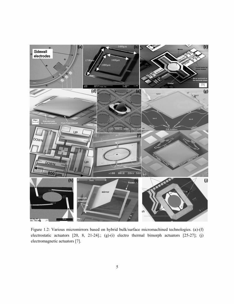
Figure 1.2: Various micromirrors based on hybrid bulk/surface micromachined technologies. ............ 5
Figure 1.3: A simple 1-D micromirror with electrostatic actuators. ....................................................... 6
Figure 1.4: Three scanning ways for Endoscopic OCT and Confocal microscope. ............................. 13
Figure 1.5: Schematic of the 3-D endoscopic OCT probe [74]. 2-D scanning MEMS mirror is putted
in front of GRIN lens. Sideimaging process ..................................................................... 15
Figure 1.6: Schematic OCT system using a fiber-optic implementation of a Michelson interferomenter
with a laser low coherence light source [66]. .................................................................... 16
Figure 1.7: Schematic diagram of a conventional confocal microscope [80]. ...................................... 16
Figure 2.1: Schematic diagram of a biaxial micromirror ...................................................................... 23
Figure 2.2: Schematic of electrostatic distribution when micromirror lies on an arbitrary tilt angle. .. 24
Figure 2.3: The layout of the four groups of electrodes........................................................................ 25
Figure 2.4: Projected angles in between the mirror plate and sidewall electrodes. .............................. 27
Figure 2.5: Four projected lines on the micromirror (=5o , =5
o) ...................................................... 30
Figure 2.6: (a) (b) (c) shows the scanning angle and Z displacement under differential drive voltage,
micromirror with bottom and sidewall electrodes. This result presents a linear relationship.
........................................................................................................................................... 32

xii
Figure 2.7: (a) (b) and (c) show the FEM simulation results: micromirror with bottom and sidewall
electrodes under differential drive. .................................................................................... 33
Figure 2.8: Pull-in voltage characteristics during -scan. ................................................................... 36
Figure 2.9: Pull-in voltage characteristics during -scan. .................................................................... 36
Figure 2.10: Capacitance versus changeable tilt angle. ........................................................................ 37
Figure 2.11: The dynamic response of -scan (solid line) and -scan (dotted line) at a bias voltage
Vbias=55V. .......................................................................................................................... 43
Figure 2.12: Resonant frequency of -scan at the different bias voltage. ............................................ 45
Figure 2.13: Resonant frequency of -scan at the different bias voltage.............................................. 45
Figure 2.14: Transient response of micromirror with sidewall and bottom electrodes. One curve
comes from scan, another from scan. The step voltage is Vs=65V. ......................... 46
Figure 3.1: Cross-section view of the micromirror with SW. ............................................................... 51
Figure 3.2: SEM of a single MEMS mirror with sidewall electrodes (micromirror with 1.5m torsion
bar) .................................................................................................................................... 54
Figure 3.3: The micromirror plate fabrication process flow. ................................................................ 59
Figure 3.4: The sidewall electrodes fabrication process flow ............................................................... 61
Figure 3.5: SEM of the sidewall electrodes .......................................................................................... 62
Figure 3.6: Schematic experimental configuration for characterizing the micromirror. ...................... 64
Figure 3.7: The linearity of the scanning angle and drive voltage for the micromirror with 3m
serpentine torsion bar ........................................................................................................ 65
Figure 3.8: The linearity of the scanning angle and drive voltage for the micromirror with 1.5m
serpentine torsion bar ........................................................................................................ 66

xiii
Figure 3.9: Scanning angle displacement under simple differential drive method for the micromirror
with 3m serpentine torsion bar. One group of curves are from micromirror with 3m
torsion bar with SW, the other from a 3m torsion bar micromirror without SW (only
bottom electrodes). ............................................................................................................ 67
Figure 3.10: Scanning angle displacement under simple differential drive method. The micromirror
with SW is based on different widths of torsion bar, 1.2m, 1.5m, and 2m. The
micromirror without SW is based on 1.5m and 2m width torsion bars ........................ 68
Figure 3.11: Large scan angle tests with simple differential drive method at- and - scan .............. 70
Figure 3.12: Electrostatic field distribution of one quadrant of the micromirror with SW under
different angular deflection ............................................................................................... 71
Figure 3.13: The frequency response of micromirror with 3m torsion bar and 1.5m torsion bar
under sinusoidal sweep experiments for a frequency range of 1Hz to 1000Hz ................ 72
Figure 3.14: The resonance frequency shifting under different bias voltages (ANSYS and
experiments) ...................................................................................................................... 74
Figure 3.15: 3D profile of the mirror with SW acquired from an Olympus LEXT OLS3100 confocal
microscope, and the distance between the mirror plate and the top of sidewall electrodes.
........................................................................................................................................... 76
Figure 4.1: The structure of 2×2 micromirror array ............................................................................. 79
Figure 4.2: The fabrication process flow of 2×2 and 4×4 micromirror arrays ..................................... 82
Figure 4.3: The front side features and critical 3-end serpentine torsion bars ...................................... 83
Figure 4.4: The backside features of the micromirror array plate after DRIE ...................................... 84
Figure 4.5: The compressive unstressed SiO2 thin film exposed after DRIE ...................................... 85
Figure 4.6: The fabrication process flow of shadow mask based on dry etching (method I) ............... 87

xiv
Figure 4.7: The fabrication process flow of shadow mask based on hybrid wet etching and dry etching
(method II) ........................................................................................................................ 88
Figure 4.8: The bulk sidewall electrodes after fabrication process ....................................................... 89
Figure 4.9: SEM of alignment mark on the SW electrodes .................................................................. 90
Figure 4.10: Photograph of 2×2 micromirror array after wire bonding in a chip carrier. ..................... 90
Figure 4.11: (a) Assemly of 4×4 micromirror array and SW electrodes; (b) SEM of 4×4 micromirror
array; (c) SEM of SW electrode array; (d) 4×4 SW electrodes after shadow mask lift-off;
(e) SEM of single micromirror with a broken serpentine torsion bar. .............................. 92
Figure 5.1: Schematic of MACROscope system with a galvo-scanner (the micromirror instead of the
galvo-scanner) [138]. DPC Detector, OFM Spectrometer, and PMT were removed from
the MACROscope system during experiments. ................................................................ 96
Figure 5.2: Optical System-I: the laser scanning microscope with a 4× beam expander. The
micromirror is located at f1 focus distance, and the entrance pupil of the objective lens at
f2 focus distance. The objective lens is M Plan Apo 5, NA=0.14, f=200. ......................... 98
Figure 5.3: Optical System-II: the laser scanning microscope with a unitary telescope. The
micromirror is located between Bi-Convex lens, f2, and the objective lens (M Plan Apo 5,
NA=0.14, f=200). The micromirror requires as close as to the entrance pupil. ................ 98
Figure 5.4: SEM of the micromirror with SW electrodes ................................................................... 100
Figure 5.5: The transient response of the micomirror with 2m torsion bars. ................................... 101
Figure 5.6: The frequency transient response of the micromirror with 2m torsion bars driven by the
triangle waveform under Vbias=50V and Vac=2.5V. The driving signal actuated the
micromirror on - and -scan, respectively .................................................................... 103
Figure 5.7: The frequency transient response of the micromirror with 3m torsion bars driven by the
triangle waveform. The driving signal actuated the micromirror on - and -scan,
respectively ..................................................................................................................... 106

xv
Figure 5.8: The pattern scanning from the micromirror with SW electrodes with 2m torsion bars.
Examples of scan pattern for various combinations of amplitude and frequency [83]. .. 106
Figure 5.9: The images in terms of the galvo-scanner without XYZ-stage movement. Two optical
systems: without Beam Expander and with 4×Beam Expander. The grate patterns are 5,
10, 20, and 50m. The galvo-scanner works at 40Hz. (Green laser source: 532nm, the
objective lens: M Plan Apo 5, NA=0.14, f=200.) ........................................................... 108
Figure 5.10: The 1-D scanning images in terms of the micromirror with 2m torsion bars. The optical
system includes a 4× beam expander with He-Ne laser source (633nm), the objective
lens: M Plan Apo 5, NA=0.14, f=200. The sample is 20m metal lines. The micromirror
only scans the 1-D scanning, at -scan, without the stage movement in order to test
synchronization under open-loop control. The frequency ranges from 30Hz to 70Hz. .. 109
Figure 5.11: 2-D images display 20m metal grate pattern. The micromirror with 2m torsion bars is
adopted in the optical system with unitary telescope (Optical System-II). The objective
lens is f-theta lens, NA=0.14, f=200mm. The light source is green laser, =532nm. The
frequency of the control signal is 40Hz. .......................................................................... 110
Figure 5.12: The laser scanning microscope system with a MEMS micromirror with 2m torsion bars.
............................................................................................................................................................ 111
Figure 5.13: The grate pattern images from LSMS on PIC LCD. The frame size is 240×320pixels. 112

xvi
List of Abbreviations
2D Two-dimensional
CLSM Confocal laser scanning MACROscope
CMP Chemical-mechanical polishing
DAQ Data acquisition
DLP Digital light projector
DMD Digital Micromirror DeviceTM
DoF Degree of Freedom
DRIE Deep reactive ion etching
DSP Double side polished
EOCT Endoscopic optical coherence tomography
FEM Finite element method
FOV Field of view
LPCVD low pressure chemical vapor deposition
LSMS laser scanning microscope system
MEMS Micro-Electric-Mechanical System
OCT Optical coherence tomography
ODE Ordinary differential equation

xvii
PECVD Plasma enhanced chemical vapor deposition
PIC Programmable interface controller
PSD Position sensing detector
RIE Reactive ion etching
SCS Single crystal silicon
SEM Scanning electron micrograph
SOI Silicon-on-insulator
SSP Single side polished
SW Sidewall

xviii
List of Symbols
d dstance between the micromirror plate and electrodes
Di torsional motion damping coefficient about axis i (i=1 for x-axis, i=2 for y-axis)
dP electrostatic force acting on the micromirror element area
E Young‘s modulus of the mirror plate material, 169GPa
E net flux of electrostatic field
Eeij flux of electrostatic field caused by electrodes eij (i =1,2,3,4; j=1,2,3)
f natural frequency of the mirror about x-axis
f natural frequency of the mirror about y-axis
FZM mechanical force on the z-axis
FE
Zeij electrostatic force along z-axis generated by electrodes eij (i=1,2,3,4; j=1,2,3)
Fz0 mechanical force caused by the mirror plate
g gap between micromirror plate and bottom electrodes
G shear modulus of the hinge material, 73GPa
Gfeij, Gfeij, integration factor caused by electrodes eij (i=1,2,3,4; j=1,2,3)
GfZeij
Ipi polar moment of inertia of hinge pair i (i=1 for x-axis, i=2 for y-axis)
Ji moment of inertia i (i=1 for micromirror inertia, i=2 for gimbal inertia)
ki spring constant of hinge pairs i (i=1,2)
l length of the torsion bars

xix
lo, lf, lp, li segment length of the torsion bars
Le distance between the parallel sidewall electrodes
Lm length and width of the micromirror plate
M0, TM0 mechanical torques caused by the mirror plate
tb thickness of the torsion bars
T mechanical torsion for x-axis
mechanical torsion for y-axis
TEeij electrostatic torsion for x-axis caused by electrodes eij (i=1,2,3,4; j=1,2,3)
TEeij electrostatic torsion for y-axis caused by electrodes eij (i=1,2,3,4; j=1,2,3)
Vbias DC bias voltage
Vx, Vy oscillating waveform voltage
Vi applied voltage (micromirror plate against electrode i) (i=1,2,3,4)
w width of the torsion bars
Greek letters
scan angle rotating about x-axis
scan angle rotating about y-axis
Γ torque around x-axis
Γ torque around y-axis
dielectric constant of vacuum, 8.854e-12 F/m
individual local coordinate along the axial length
projected angle between the micromirror plate and the bottom electrodes
wavelength
density of the micromirror plate material, 2329 Kg/m3

xx
normalized time
projected angle between the micromirror plate and the sidewall electrodes

1
Chapter 1
Background and Thesis Overview
1.1 Introduction
Micro-Electro-Mechanical Systems (MEMS) micromirrors have been developed for more than two
decades along with the development of MEMS technology [1]. Various MEMS devices, such as ink
jet printhead, inertial sensors, pressure sensors, accelerators, gyroscopes, RF switches, resonators, and
micromirrors, have been exploited. MEMS mirrors are the intensive research field among these
devices. They are considered the leading technology for many application fields, such as in adaptive
optics (AO), optical switches, digital light projector (DLP), high-definition (HD) laser display,
barcode reader, optical coherence tomography (OCT), and confocal microscopes [2–10]. The
performances and limitations of these devices are highly dependent on MEMS mirrors in systems.
Particularly, there has been intensive research on integrating MEMS mirrors into an endoscopic
optical coherence tomography (EOCT) system or confocal microscope. Design and fabrication of a
biaxial micromirror that is capable of large 2 Degree-of-Freedom (DoF) angular scans with low
driving voltages for endoscopic application and confocal microscope is the motivation of this thesis.
In this thesis, a 2-D Silicon-on-insulator (SOI) MEMS micromirror with sidewall (SW) electrodes
for imaging is presented. A theoretical model of SW electrodes for a biaxial micromirror is developed.
Subsequently, a novel fabrication process is developed to fabricate a biaxial micromirror with SW
electrodes. The static and dynamic characteristics of the micromirror with SW electrodes are

2
exploited. The process is also extended to fabricate micromirror arrays. Finally, a biaxial micromirror
with SW electrodes is applied into Confocal MACROscope (from Biomedical Photometrics Inc.
(BPI), Waterloo, ON) for imaging.
1.2 MEMS Mirror Overview
Various MEMS mirrors are achieved through a combination of two broad micromachining
technologies, surface or bulk micromachining techniques. They possess a number of attractive
features, such as extremely compact structure size, small weight, potential low power and low cost,
high reliability, and batched fabrication. MEMS mirrors have a large scale range from several
micrometers to millimeters and a wide bandwidth in worked frequency from a low frequency (Hz) to
a high frequency (kHz) in terms of different fabrications and applications. Recently, various
commercial fabrication processes are developed successfully, such as Poly-MUMPs, SOI-
MUMPs&Metal-MUMPs (provided by MUMSCAP), SUMMiT-V, DMD (from Texas Instrument Inc.
(Dallas, TX)), Optical iMEMS process (from Analog Devices Inc.), and IntelliSense technology.
However, each fabrication process has its own specification and limitation for a certain application.
Thus, it is necessary to develop a novel fabrication process for a biaxial micromirror with SW
electrodes that is applied into Endoscopic OCT and confocal microscope.
By studying various MEMS mirrors, their basic characters can be derived and listed as the
following:
Fabrication processes based on surface micromachining or hybrid bulk/surface
micromachining techniques
Different materials adopted by micromirrors
Various actuation mechanisms
Self-assembly, assembly, or non-assembly processes for micromirrors
1-D, 2-D, or 3-D micromirrors with gimbal or gimballess structures
Micromirror functions in optical systems: Digital, analogue, or fixed mirror

3
In fact, although developing a sophisticated micromirror is very complicated, it is possible to reach
the goal by grasping the fabrication process and actuation mechanism of the micromirror in terms of
requirements of an application. A typical micromirror is composed of a movable mirror plate,
supporting frames, and actuators.
1.2.1 Surface & Bulk Micromachining Techniques
The main techniques in MEMS technology are composed of surface micromachining and bulk
micromachining. Surface micromachining techniques leave the wafer untouched, but add/remove
additional layers above the wafer surface, first widely used in 1990‘s, while bulk micromachining
techniques involve removing material from the silicon wafer itself [11]. Figure 1.1(a), (b), and (c)
show three types of micromirrors based on surface micromachining. As shown in Figure 1.1(a), the
micromirror is fabricated in terms of SUMMiT-V technique. Multiple layers are deposited and
patterned [12]. An upper spring and a lower spring support the mirror plate. The bottom electrodes
(electrostatic actuators) drive the mirror plate to rotate along two directions. Figure 1.1(b) shows a
micromirror array and an electrostatic actuator in a DMD chip. The electrostatic actuator actuates the
micromirror to realize ―on‖ or ―off‖ mode [13, 14]. A micromirror in Figure 1.1(c) is fabricated by
surface micromachining. The mirror plate is elevated through a self-assembly process after all
fabrication processes; therefore, a large gap between the mirror plate and bottom electrodes is created
[15]. The main advantage of surface micromachining techniques is that it is compatible with CMOS
process easily and suitable to obtain a large micromirror array, however, the thickness of each layer
on the substrate has a limitation less than 2-3m. As a result, it is difficult to get a thicker mirror plate
than deposited layers. The curvature of the mirror plate is large and the scanning angle is small [16,
17]. Moreover, the release process requires a bunch of etching holes on the surface of the mirror plate.
Those holes degrade the optical properties [18, 19].
Hybrid bulk/surface micromachining techniques are widely adopted by various micromirrors, as
shown in Figure 1.2. Combining with SOI technology, bulk micromachining easily obtains a thick

4
(a) (b)
(c)
Figure 1.1: MEMS mirrors based on surface micromachining techniques. (a) A micromirror in terms
of SUMiMT-V; (b) A DMD from Texas Instrument; (c) A micromirror with elevating self-assembly
process.
5
Figure 1.2: Various micromirrors based on hybrid bulk/surface micromachined technologies. (a)-(f)
electrostatic actuators [20, 8, 21-24].; (g)-(i) electro thermal bimorph actuators [25-27]; (j)
electromagnetic actuators [7].

6
mirror plate and a large cavity on the substrate, so various complex micromirrors employ hybrid
bulk/surface micromachining techniques. From Figure 1.2 (a) to (f), electrostatic actuators actuate the
mirror plate which has a large size and a low curvature to get 2-D scanning. Electro thermal bimorph
actuators are used in some micromirrors, as shown in Figure 1.2 (g), (h), and (i). Electromagnetic
actuators are adopted by the micromirror in Figure 1.2(j). The micromirrors in Figure 1.2(a), (c), (d),
(f), (g), (h), and (i) require non-assembly process, while, those in Figure 1.2(b), (e), and (j) need an
assembly process.
1.2.2 Materials in MEMS Mirrors
Various materials adopted by MEMS mirrors enrich fabrication processes and designs. Kurt Peterson
states single crystal silicon as a perfect mechanical material in MEMS devices [28]. In
micromachining, silicon, glass, ceramics, group III and V elements are important substrate materials.
A variety of metals including titanium, platinum, tungsten, aluminum, gold, chrome, nickel, copper,
and so on, are used widely as thin deposited films. Meanwhile, silicon dioxide, silicon nitrides, silicon
carbides, carbon, and polymers (Polyimide, PMMA, SU-8, and parylene, and so on) are also
deposited as thin films.
Figure 1.3: A simple 1-D micromirror with electrostatic actuators.

7
For example, a very simple 1-D micromirror with electrostatic actuators is composed of a movable
mirror plate, torsion bars, support frames, and electrodes, as shown in Figure 1.3. Generally, materials
of the mirror plate could be silicon, polysilicon, polymers, SU-8 or parylene [29], and the torsion bars
may be based on silicon, polysilicon [23], silicon nitride [8], metals [30], polymer [5], or SU-8 [31].
The substrate could be silicon or glass. Metal thin films, aluminum or gold, are patterned on the
substrate to form bottom electrodes. Depositing titanium/gold or chrome/aluminum on the surface of
the mirror plate improves the ratio of light reflecting. Subsequently, the support frame with the mirror
plate mounts on the substrate by flip-chip or bonding process. If the micromirror adopts different
actuators, its corresponding materials and fabrication process have to be selected in terms of the
specialty of the actuator.
1.2.3 Actuation Mechanisms
The design, fabrication, and characteristics of MEMS mirrors are highly dependent on actuation
mechanisms. Actuation mechanisms include electrostatic, electro thermal bimorph, electromagnetic,
PZT, electrowetting, and hybrid types. Table 1.1 illustrates the outline of different MEMS actuators
used in MEMS mirrors from literatures. It is very important to understand various actuation
mechanisms for selecting micromirror structures and fabrication processes when a new micromirror is
developed for a special application.
1.2.3.1 Electro Thermal Bimorph Actuator
The thermal bimorph actuator is formed by using two materials with the thermal coefficient of
expansion (TCE) difference. The bimorph tip performs an angular rotation due to both the residual
stress and the TCE difference of two materials. The bimorph actuator is composed of either double
layers with the TCE difference, such as Al/SiO2, Au/SiO2, metal/silicon nitride, Ni/Ni-diamond [32],
or Al and SiO2 enclosing the polysilicon or Pt heater [7, 25, 33, 34]. The bimorph actuator drives
MEMS mirrors to perform either one direction (upward or downward) deflection [6, 26, 27], or dual
direction movements in terms of dual S-shape bimorph [25, 34]. Its fabrication process is compatible

8
with CMOS sequences. The micromirror with thermal bimorph actuators can be built on one piece of
single-crystal-silicon (SCS) wafer or SOI wafer entirely, so that an assembly process is avoided. In
order to create an out-of-plane curling structure, the amount of fabrication experiments are required,
but it is difficult to control curling angles after the mirror plate is released.
The main disadvantages of thermal actuators are high power consumption, low actuation speed, and
material degradation and fatigue due to thermal stress cycles for a long period of time. The hysteresis
phenomenon can be observed due to the thermal relaxation time [7]. In addition, the design of heat
sink is a basic requirement for bimorph actuators [33]. The thermal resistance of bimorph actuators
depends on the heat-flow path from the actuator to the substrate. This requires a sophisticated design.
1.2.3.2 Electromagnetic Actuator
Electromagnetic actuators utilize the Lorenz force, F=I×B, generated when the electric current, I,
pass through the coils in the external electromagnetic field with the magnetic flux density, B. Those
actuators are created by either fabricating incorporated actuation coils or depositing ferromagnetic
materials such as nickel-iron on the movement portion of devices [6, 10, 35-45]. In order to obtain the
external electromagnetic field, some magnetic actuators use external permanent magnets or
electromagnets while others use deposition and patterning of hard magnetic materials during the
fabrication [41, 43, 44]. Therefore, the electroplating process is very common to fabricate thick coils
or ferromagnetic materials for those actuators. Usually there is an assembly process for the last step
after fabricating all the components. Magnetic actuation technique can deliver sufficient torque to
allow a mirror plate to scan a large angle, thus, the size of the mirror plate can be designed in several
millimeters and the spring hinge could have high spring stiffness [6]. Although the drive voltage is
small, the current is high (in the range of milli-amps(mA)) comparing with other actuators. Such
actuator generates a lot of heat during work duration. Its disadvantage is potentially poor hysteresis
and fatigue performance, which could affect static pointing accuracy and reliability. Most of
micromirrors can realize 1-D scan [10, 37, 38], while some of micromirrors perform 2-D scan [35, 40,
43, 44].

9
1.2.3.3 Piezoelectric Actuator
Piezoelectric actuators utilize the piezoelectric effect, that is, when electric field applies to the class of
materials, a piezoelectric thin film causes a strain to transverse direction by its inverse piezoelectric
effect. Usually, a piezoelectric actuator has a metal/piezoelectric material/metal sandwich structure
stacked on an insulation layer [47-52]. Pb(Zrx,Ti1-x)O3 (PZT) is present general preferred
piezoelectric material. The fabrication process is pretty simple, but requires depositing ferroelectric
layers by sol-gel process and high Curie temperature [46]. When the exciting displacement frequency,
that is applied electric field frequency, agrees with the resonant frequency of bending or torsional
mode of a MEMS mirror, the mirror plate is actuated at the resonant vibration on each mode [47, 49].
Piezoelectric hysteresis and polarization are the main consideration during the design and fabrication
[50]. In addition, since the piezoelectric actuator forms a capacitor, the leakage current is another
characteristic during the design and fabrication. Zara et al. [48] adopted the piezoelectric bimorph as
an actuator to drive the micromirror rotate about pivot axis by polyimide hinge for an endoscope.
1.2.3.4 Electrowetting Actuator
Electrowetting (EW) and Electrowetting-on-dielectric (EWOD) actuation are principles that control
the shape of electrolyte drops on an electrode plate using electric potential [53, 54]. When a mirror
plate is assembled on liquid droplets, the movement of the plate is generated by the shape change of
droplets. The liquid metal drop (LMD) has several advantages over an electrolyte drop as a pivot of a
micromirror: lower vapor pressure, less electrolysis, and better electrical/thermal contact with the
substrate and the mirror. Mercury drop and gallium drop have been tested by Zeng et al. [53]. The
insulation layer thickness between the LMD and the electrode plate affects the behavior of liquid
metal drops. The micromirror plate and the electrodes are assembled with the LMD at their ―confine
spot‖—a wetting metal spot surrounded by nonwetting parylene insulating surface treated by argon
sputter. With the confine spot, the LMD drop can adhere strongly to the mirror plate and the substrate.
Although the micromirror with electrowetting actuator can realize piston movement, it is essential to

10
realize the 2D rotation as well. The drive voltage is high. There is no any report about this kind of
actuators for endoscopes in literatures.
1.2.3.5 Hybrid Microactuator
Hybrid microactuators combine two types of actuators or more to compensate disadvantages of
individual actuators. Several hybrid actuators are developed: i) electromagnetic and electrostatic; ii)
electromagnetic and electrothermal; iii) electrothermal and electrostatic. Il-Joo Cho et al. [55] used
electromagnetic and electrostatic actuators into a RF-MEMS switch in order to obtain low power and
low voltage operation. Youngkee Eun et al. [56] fabricated a micromirror with an electrothermal and
electromagnetic actuator that generates a buckling deformation by the electrothermal actuator and
control the buckling direction by the electromagnetic actuator in static mode. A RF-MEMS switch
using electrostatic and electrothermal microactuators was fabricated by Ph. Robert et al. [57].
Moreover, Aravind Alwan et al. [58] gave an analytical modeling and figured out advantages of
electrostatic and electrothermal actuation theoretically.
1.2.3.6 Electrostatic Actuators for MEMS Mirrors
Electrostatic actuators exploit the difference in electrostatic forces between two electrodes. Generally,
there are two common electrostatic actuators: (i) parallel-plate; and (ii) comb-drive. Most
micromirrors adopt parallel-plate actuators. They are actuated by high voltages and have a small tilt
angle range. Therefore, the reduction of driving voltages while increasing the tilt angle range is a core
requirement for the next-generation of electrostatic scanners. Traditionally, a biaxial micromirror is
actuated by either four separate bottom electrodes [15] or by two inner bottom electrodes on the
micromirror and two outer bottom electrodes on the outer attraction plates of the micromirror [8].
Meanwhile, a number of micromirrors adopt comb-drive actuators [59-63], which are built on the
multiple SOI wafers and wafer bonding technology. In order to fabricate two layers of comb fingers

11
Table 1.1: Characteristics of different typical actuators used in the micromirrors
Characteristics Different actuators based on different physical basis Electromagne
tic1
Bimorph
electrothermal
Piezoelectric (PZT) Electrowetting Electrostatic
Comb drive Parallel plate
Physical basis The Lorentz
force
F=I×B
Two metals
with different
thermal
expansion
coefficient
An electrical
resistor may
change its
resistance when it
experiences a strain
and deformation
R=pl/A
Liquid metal drop
changing shape at
electric field
2
1
012
2coscos u
d v
Electrostatic
force,
fringe field
effect
An electrostatic force
between the two
parallel plates
2
2
1V
x
CF
Substrate SCS, SOI SCS, SOI SCS SCS, SOI SCS, SOI
Voltage low low high high low high
Current large large small small small
Power
consumption
high high low low low
Response time fast slow fast fast fast fast
Scan angle2 large large small small large small
Scan mode 1D, 2D 1D , 2D 1D, 2D 1D, 2D 1D , 2D 1D, 2D
Assembly3 yes no no yes yes yes
Structure
character4
gimbal gimbal gimbal gimballess gimbal,
gimballess
gimbal,
gimballess
Fabrication
process
complex complex complex simple complex, simple
Notice:
1. Electromagnetic actuators have a shielding requirement and require the fabrication of ferromagnetic materials, and hence increase the
overall size of the micromirror system;
2. Scan range comes from literatures, and the biggest scan angle bases on the real application;
3. Assembly is a process integrating the micromirror plate with the actuators;
4. Structure of the micromirror can be divided into gimbal and gimballess. Gimbal structure increases the overall size and has a low fill
factor, and gimballess structure decreases the overall size and has a high fill factor.

12
with different height, a sophisticated fabrication process has to be employed. One group of comb
fingers realize either upward or downward movement, thus, the design of micromirrors with comb
drive actuators often require a large area to accommodate the actuators and thereby increase the
overall device size. More details of electrostatic actuators are presented in subsequence chapters.
Various micromirrors with different actuators in EOCT and confocal microscope have been
developed. When compared with these actuators, as listed in Table 1.1, electrostatic actuators are easy
to be understood and simple to realize. Therefore, this thesis focuses on developing a micromirror
with electrostatic actuators.
1.2.4 Single Micromirror & Mirror Array
From single micromirror to micromirror arrays, they apply to DMD, optical switches, adoptive optics
(AO), and optical phased array, and so on. Moreover, a micromirror array requires more sophisticated
fabrication process than that of single micromirror. In a digital device such as a DMD chip, thousands
of micromirrors are integrated at a small area. The reliability, yield rate and fill factor are important
parameters. On the other hand, a micromirror array divides a large aperture into small apertures in
order to keep the frequency bandwidth. In this thesis, the fabrication process is developed from single
micromirror fabrication to micromirror array fabrication. Another important work is to calibrate each
micromirror on an entire mirror array chip.
1.3 MEMS Mirrors in Endoscopic OCT and Confocal Microscope
Endoscopic OCT (EOCT) and confocal microscope employ MEMS mirrors to build laser scanning
imaging systems. Generally, there exists three ways to perform laser beam scanning: i) beam scanning
before the objective lens (Pre-Objective Scanning); ii) beam scanning after the objective lens (Post-
Objective Scanning); iii) objective lens scanning. Figure 1.4 shows these three scanning
configurations. MEMS mirrors are often used for the first two scanning ways, while MEMS
microlenses or optic fiber bundles are adopted for the third one [8, 10, 64]. In this thesis, a biaxial
micromirror with SW electrodes that is based on electrostatic actuation mechanism is mainly used

13
Figure 1.4: Three scanning ways for Endoscopic OCT and Confocal microscope.
into the first two ways. The goal of the thesis is to design and fabricate a biaxial micromirror for
EOCT or Confocal MACROscope, which is a Confocal Laser Scanning Microscope (CLSM) with a
large field of view (FOV) procured from Biomedical Photometrics Inc (BPI), Waterloo, ON. In order
to integrate a micromirror with an endoscopic probe, there are several requirements the micromirror
should process:
Satisfies the endoscopic dimensional requirements: An endoscope has strict requirements on
its diameter that is dependent on its application. In an endoscopic OCT system, the
endoscopic probe is inserted into the human body; therefore the diameter of the endoscope
will determine the diagnostic limitations. There are two scan modes: (i) side-imaging; and (ii)
forward-imaging, for an endoscopic probe. The outer diameter of a side-imaging probes
ranges from 0.4mm to 5mm, and that of forward-imaging probes range from 1.65mm to

14
7.5mm [65]. The dimensions of the micromirror have to be compatible with the diameter of
the endoscopic probe.
Provides a large scanning angle under a low driving voltage: The drive voltage actuating the
micromirror is a safety concern when the endoscope is inserted into the human body. A larger
angular scan will be able to create a larger field-of-view. Hence, physicians are able to image
a larger piece of tissues within a shorter duration of time. This will greatly reduce the
diagnostic time of the patient.
Capable of 2 DoF scans: Combining a fast scan with a slow scan creates 2-D raster scan.
Needs a large micromirror plate in order to obtain high resolution images.
Requires simple fabrication processes that are compatible with MEMS fabricating
technology.
1.3.1 Endoscopy, OCT and Confocal Microscopy
Endoscopic probes can be integrated with either OCT system or confocal microscope. Endoscope
based on MEMS mirrors with a sophisticated optical system performs the laser beam scanning and
collects reflected light that is excited or emits from the tissue or samples back to an optical fiber. Only
a general discussion of selected fundamental concepts of endoscopy, OCT system and confocal
microscopy is given here, for more detailed discussion see [66, 67].
1.3.1.1 Endoscopy
An endoscope is a probe for performing the laser scanning and also detecting scattered or reflected
light. It is not only a diagnostic tool but it can also be used as a therapeutic equipment [65]. There are
two typical endoscopes: (i) capsule endoscope; and (ii) catheter endoscope. The latter is our focus. A
compact MEMS mirror is well-suited for endoscope applications because of its limited small
dimension by MEMS technology. Scanning methods are of the utmost importance for endoscope
probe. Generally, the scan modes can be divided into forward imaging and side imaging probe. Other
important technical characteristics of an EOCT probe are the mirrors‘ scanning range, field-of-view
(FOV), speed, and scanning flexibility.

15
Various endoscopes based on MEMS technology are being developed by many groups around the
world [7-9, 26, 27, 68-75]. The typical structure of an MEMS-based endoscope is shown in Figure 1.5.
The probe consists of a biaxial MEMS mirror and pigtailed gradient index (GRIN) lens mounted in
tubular steel housing [74]. The optical fiber transmits light to the MEMS mirror and receives the
scattered light from the tissues through the MEMS mirror again. The Optical fiber, GRIN lens, and
the MEMS mirror are positioned so that the noise generated in the scanning head minimized. By
monitoring the noise and minimizing it, high precision assembly within an error of few microns could
be achieved [24].
Figure 1.5: Schematic of the 3-D endoscopic OCT probe [74]. 2-D scanning MEMS mirror is putted
in front of GRIN lens. Sideimaging process
1.3.1.2 OCT System
An OCT system is based on a fiber-optic Michelson interferometer to obtain high-resolution
noninvasive cross-sectional imaging of tissue microstructure [66, 76-79]. OCT is an optical imaging
technique that is analogous to ultrasound B-mode imaging and operates using continuous wave short
coherent length light and can image the cellular structure of tissues at depths greater than
conventional microscopes [66]. Light reflected from scattering sites within a sample is localized in
depth by low-coherence interferometry. The low coherence interferometry measures the
electromagnetic field of the optical beam rather than its intensity, since when two beams of light are
combined, their fields rather than their intensities add and produce interference. Scanning a reference
delay line while recording the interferometric detector response creates a map of reflectivity relative
to optical depth. Here, the detector measures the intensity of the output optical beam, which is

16
proportional to the square of the electromagnetic field [66]. Two-dimensional images are made from
sequential longitudinal image lines of backscatter versus distance into the sample. OCT produces
tomographic images of subsurface microscopic structures with a resolution of 10m or less [77, 79].
The performance of OCT systems varies widely according to their design and data acquisition speed
requirements [66].Figure 1.6 shows the schematic OCT system.
Figure 1.6: Schematic OCT system using a fiber-optic implementation of a Michelson interferomenter
with a laser low coherence light source [66].
Figure 1.7: Schematic diagram of a conventional confocal microscope. The screen with the pinhole
lies in the back focal plane of the sample with respect to the objective, thus rejecting most out-of-
focus light. The rotating mirrors scan the sample pixel by pixel, and are the rate-limiting step for
obtaining an image [80].

17
1.3.1.3 Confocal Microscopy
Confocal microscope is an optical imaging technique used to increase micrograph contrast and/or to
reconstruct 3D images by using a spatial pinhole to eliminate out-of-focus light or flare in specimens
that are thicker than the focal plane [67]. Figure 1.7 illustrates the schematic diagram of a
conventional confocal microscope. In this system, a biaxial micromirror can replace the two scanning
mirrors and realize the same function. More details of confocal microscope with MEMS mirrors will
be discussed in Chapter 5.
1.4 Thesis Organization
The organization of this thesis is as follows. Chapter 1 contains the research background and
micromirror overview. Developing a biaxial MEMS mirror applied into EOCT and confocal
microscope is the motivation of this thesis. Chapter 2 presents a characteristic study of a micromirror
with SW electrodes. An analytical modeling of SW electrodes for a biaxal micromirror is developed.
Chapter 3 contains the design, fabrication and characterization of a 2-D micromirror with sidewall
electrodes. Micromirrors with 3m and 1.5m serpentine torsion bars are successfully fabricated.
Chapter 4 describes the fabrication process of 2×2 and 4×4 micromirror array with SW electrodes.
Chapter 5 presents the micromirror with SW electrodes for the MACROscope imaging and a
Micromirror-based Laser Scanning Microscope System. As the system developed is still at the proof
of concept phase, a discussion on future directions is found in Chapter 6. Appendix A contains a list
of integral factors.
1.5 Author‘s Contributions
The work in Chapter 2 was published in International Journal of Optomechatronics, Vol. 1, No. 3,
pp231-258, July 2007 [81]. The author created an analytical modeling of SW electrodes so as to
simulate the static and dynamic characteristics of a micromirror with SW electrodes. The linear
voltage-to-angle property is still maintained under differential drive method and the drive voltage to

18
achieve the same angular displacement is greatly reduced. The pull-in voltage is not changed
significantly. As a novel electrostatic actuator, using SW electrodes is the main consideration for
design and fabrication of a micromirror.
The work in Chapter 3 was published in IEEE Journal of Microelectromechanical Systems, Vol. 19,
No. 3, pp619-631, June 2010 [82]. The author designed and fabricated a 2 Degrees-of-Freedom (DoF)
silicon-on-insulator (SOI) MEMS mirror with SW electrodes. The biaxial MEMS mirror with SW
electrodes is actuated by electrostatic actuators. The dimension of mirror plate is 1000m×1000m,
thickness 35m. The extended analytical modeling, fabrication process, and performance
characteristics are described. The chapter analyzes the effects of the 3-end single crystal serpentine
torsion bar width and the bottom electrodes and SW electrodes on the performance of the mirror. A
new fabrication process based on SOI wafer, hybrid bulk/surface micromachined technology, and a
high aspect ratio shadow mask is presented. In comparison to previous fabrication processes and the
Optical iMEMS®
process, the process is novel, easily understood, and simple to realize. The measured
maximum angular deflection achieved is ±11º (mechanical angle) at a static operating voltage and
±21º (mechanical angle) at a resonance frequency driving.
Chapter 4 devotes to extend the fabrication process of the single micromirror with SW electrodes to
fabricate micromirror arrays. Four depths on the backside of the SOI wafer by DRIE process, two
methods to fabricate the shadow mask, and sophisticated assembly process are the outstanding
features. After optimization of the design and fabrication process, 2×2 and 4×4 micromirror arrays are
obtained successfully. Although the fabrication of micromirror arrays is more difficult than that of the
single micromirror, micromirror arrays achieved prove that the novel well-designed process possesses
a flexibility and feasibility. The single micromirrors with SW electrodes, 2×2 and 4×4 micromirror
arrays are fabricated at Cornell NanoScale Science & Technology Facility (CNF), Cornell University,
USA.
The development of Micromirror-based MACROscope and a prototype of Micromirror-based Laser
Scanning Microscope System are founded in Chapter 5. A biaxial MEMS mirror with SW electrodes
at first time was tested in the MACROscope for the purpose of simplifying the MACROscope system.
19
This work cooperates with BPI. The study of optical requirements figures out optimizations on
frequency and scanning range of the micromirror. In terms of experiment results from Micromirror-
based MACROscope, the Micromirror-based Laser Scanning Microscope System is developed and 2-
D images are obtained. This mirror is well-suited for applications where these characteristics are
critical, such as in endoscopic scanning elements.
Some data in Chapter 3, Chapter 4, and Chapter 5 are from the paper ―A 2-D micromachined SOI
MEMS mirror with sidewall electrodes for biomedical imaging‖, which has been published by
IEEE/ASME Transactions on Mechatronics, Vol. 15, No. 4, pp501-510, 2010 [83].
Except as noted, all the experiments were performed in Professor John Yeow‘s laboratory at the
Advanced Micro-/Nano- Devices Lab/University of Waterloo.

20
Chapter 2
A Characteristic Study of Micromirror with
Sidewall Electrodes
2.1 Introduction
The Optical Microelectromechanical System (MOEMS) scanner is one of the core components in
many interesting fields as laser imaging, information handling, factory automation, printing, graphic
arts, image digitizing, quality inspection, barcode reading, data storage, precision pattern generation,
display, surveillance, and medical imaging [7, 13, 84-86]. It usually determines the device‘s limitation
and performance. A biaxial micromirror used in an Optical Coherence Tomography (OCT) system to
acquire 3-Dimensional images has already been demonstrated [8]. In addition, the micromirror
actuating mechanisms such as electrostatic, thermal [26, 27, 87], piezoelectric [47, 88],
electromagnetic [7], electrowetting of liquid metals [53] or hybrid actuators, are the subjects of
intense research. During the actuator design process, performance such as static and dynamic
characteristics of the scanner should be modeled, simulated, and understood [89, 90]. Several papers
have reported the methodology on how to design a micromirror device [91-93].
Electrostatic actuator is widely used in many micromirror designs. The principles of electrostatic
actuator are well-understood and their designs are simpler than other typical actuators. Electrostatic
actuators are easy to fabricate by traditional integrated circuit (IC) process. There are two common
electrostatic actuators: (i) parallel-plate; and (ii) comb-drive. Although parallel-plate actuators are

21
only capable of relatively small tilt angles under a high voltages in comparison to comb-drive
actuators, their fabrication process are fairly straightforward, simple to be realized.
For parallel-plate actuators, the electrode configuration has a significant effect on the drive voltage
threshold. Two typical electrode configurations have already been demonstrated: (i) planar electrode
configuration [8, 9, 59-63]; (ii) inclined electrode configuration [94, 95]. The first configuration is
very popular, and the second one is used by a handful of designers. Based on the electrostatic force,
F=1/20AV2/d
2, (0 – dielectric constant of vaccum, A – effective area, d – the distance between
electrode and mirror plate), if the same drive voltage is used, an increase in d will decrease the
electrostatic force rapidly. Meanwhile, increasing the effect area of electrodes is effective to raise the
electrostatic force. As a result, micromirrors with sidewall electrodes are proposed in Pu et al. [20].
Although the effect of bottom electrodes is well understood [8, 15, 96], there is no theoretical model
to describe the effect of sidewall electrodes on a biaxial micromirror [97, 98]. The purpose of
combining sidewall electrodes with bottom electrodes is to increase the electrostatic force on the
micromirror plate. In this configuration, the static and dynamic behaviours of micromirrors deserve
more investigation and detailed analyses.
In this chapter, a micromirror with a combination of sidewall and bottom electrodes will be
modeled and investigated. Theoretical electrostatic model on a micromirror with sidewall and bottom
electrodes are derived and simulated. Design parameters such as the controllable tilt angle, the pull-in
angle and dynamic characteristics-modal analysis are studied to determine the desired scanner designs.
All analytical design results are compared with Finite Element Modeling (FEM) simulations.
2.2 The Theoretical Modeling of Micromirror with Sidewall Electrodes
2.2.1 Building a Theoretical Modeling of Micromirror with Sidewall Electrodes
Generally, a biaxial micromirror consists of a rigid mirror plate, spring hinges, supporting frames and
actuating electrodes. A micromirror structure is shown in Figure 2.1. The micromirror is suspended
by the double-gimbal structure, which consists of two pairs of torsion bars (straight beam) for 2-
22
Degree-of-Freedom (DoF) scans: -scan and -scan, which rotates about the X-axis and Y-axis
respectively. The micromirror plate is electrically grounded and the quadrant electrodes (sidewall and
bottom electrodes) offer V1, V2, V3 and V4 voltages. The parameters of the micromirror are listed in
Table 2.1.
In order to simplify the electrostatic force model between the micromirror and sidewall electrodes
and bottom electrodes, we made several assumptions, namely:
Ignore the electrostatic fringe field effect
Electrostatic force caused by the bottom electrode will act on the entire micromirror plate
Electrostatic force caused by the sidewall electrode is divided into upper sidewall electrostatic
field and lower sidewall electrostatic field, as shown in Figure 2.2. The upper sidewall
electrostatic field on the micromirror plate is ignored when tilt angle is small
2.2.1.1 Define the Coordinate System
Although the models for vertical electrode configuration are deduced in [97, 98], there is no existing
models to describe 2 DoF configuration. The coordinate systems are defined: (i) global coordinate
system (XYZ); and (ii) body-fixed coordinate system (xyz). Global coordinate system is fixed on the
substrate and the origin of body-fixed coordinate system is set on the centre of the micromirror plate.
These definitions are the same as Toshiyoshi et al. [15].
A small area (dS) on the mirror in the body-fixed coordinate system, A(x, y, 0), and the normal
vector of the mirror, m=(0, 0, 1), in Figure 2.3, are transferred to the global coordinate system, and
corresponding coordinate A and vector m are represented by:
sinsincos,cossinsin,cos yxyxxA (2.1)
and
coscos,cossin,sin m (2.2)
respectively (see, e.g., (Toshiyoshi et al. [15]).

23
Figure 2.1: Schematic diagram of a biaxial micromirror (a) 3D diagram, mirror plate rotates about
inner torsion bar, y-axis (-scan); gimbal frame with mirror plate that rotates about outer torsion bar,
x-axis (-scan). (b) cross sectional view.

24
Table 2.1: Parameters of the biaxial micromirror
Paremeters Variable Value
Micromirror properties
Mirror width Lm 400m
Mirror length Lm 400m
Mirror plate thickness tm 1.5m
Gimbal width Lgw 580m
Gimbal thickness tg 1.5m
Gimbal length Lgl 900m
Torsion bar width w 2m
Torsion bar thickness tb 1.5m
Torsion bar length l 200m
Electrode bottom edge
width
Le 450m
Gap g 75m
Assumed material properties
Young‘s modulus E 169 Gpa [99]
Shear modulus, G 73 Gpa
Silicon density, ρ 2329 kg/m3
Air permittivity, 0 8.854e-12 F/m
Figure 2.2: Schematic of electrostatic distribution when micromirror lies on an arbitrary tilt angle.

25
Figure 2.3: The layout of the four groups of electrodes.
Note that the four group electrodes, e11 e12 e13 , e21 e22 e23 , e31 e32 e33 , and e41 e42 e43 are shown in
Figure 2.3. When the micromirror plate is inclined, we can define the angles between the micromirror
plate, and the bottom electrodes and the sidewall electrodes by , , and respectively. The
maximum slope angle of the mirror to the bottom electrode, , is equal to the angle between the
normal vector of the mirror, m and the Z-axis (Z=(0,0,1)) (Toshiyoshi et al. [15]). In addition, as
shown in Figure 2.4(a), the maximum slope angle of the mirror to the sidewall electrode (e12), , is
equal to the angle between the normal vector m and the Y-axis (Y=(0,1,0)); in Figure 2.4(b), the
maximum slope angle of the mirror to the sidewall electrode (e13), , is equal to the angle between
the normal vector m and the X-axis (X=(1,0,0)). Therefore, we take the inner product of them to
find , , and as follows:
coscoscos Zm , so coscoscos,1
(2.3)
cossincos Ym , so cossincos,1
(2.4)
sincos Xm , so )(sincos,1
(2.5)
2.2.1.2 Electrostatic Force on one Element of the Micromirror Plate

26
Since the flux of electrostatic field is perpendicular to the mirror surface, an element, dS, in Figure 2.3,
on the mirror is attracted by electrostatic force from both the bottom electrode and the sidewall
electrodes. Therefore, the net flux of electrostatic field E is approximately
E ≈ Ee11+Ee12+Ee13 (2.6)
for one quadrant of the mirror plate, where Ee11, Ee12 and Ee13 are the flux of electrostatic field caused
by the electrodes, e11, e12 and e13, respectively.
The electrostatic pressure is defined by:
2
0
2
02
1
2
1
d
VEF (2.7)
= 8.854×10⁻¹²
- dielectric constant of vacuum. The electrostatic force on the element, dS, is
dAd
VdSEdP
2
0
2
02
1
2
1
(2.8)
The moments of electrostatic force on the micromirror plate are
ydPdT
(2.9)
and
xdPdT
(2.10)
y represents the moment direction based on the global coordinate system.
The electrostatic flux caused by sidewall electrodes on the element, dS, can be derived as
cossinsin2
)sin(
)()sin(
12
12
yxLe
V
AQ
V
AA
V
d
VE e
(2.11a)
cos2
)sin(
)()sin(
13
13
xLe
V
AQ
V
AA
V
d
VE e
(2.11b)

27
Figure 2.4: Projected angles in between the mirror plate and sidewall electrodes.
The moment of electrostatic force from sidewall electrodes on the micromirror rotating about X-
axis (-scan) are:
12
2
0
12
2
2
012
2
1
cossinsin2
1)sin(
2
1ef
Se
EGVdxdy
yxLeyVVT
(2.12a)
13
2
0
13
2
2
013
2
1
cos2
1)sin(
2
1ef
Se
EGVdxdy
xLeyVVT
(2.12b)

28
The moment of electrostatic force from sidewall electrodes on the micromirror rotating about Y-
axis (-scan) are:
12
2
0
2
12
2
012
2
1
cossinsin2
1)sin(
2
1ef
Se
EGVdxdy
yxLexVVT
(2.13a)
13
2
0
2
13
2
013
2
1
cos2
1)sin(
2
1ef
Se
EGVdxdy
xLexVVT
(2.13b)
Moreover, the micromirror plate is pulled down along Z direction, so the entire electrostatic forces
caused by the e12 and e13 electrodes along Z-direction are the sum of components: dPe12cos(/2-) and
dPe13cos(/2-), respectively.
12
2
0
2
12
2
012
2
1
cossinsin2
1)sin()2/cos(
2
1fZe
Se
ZeE
GVdxdyyxLe
VVF
(2.14a)
13
2
0
2
13
2
013
2
1
cos2
1)sin()2/cos(
2
1fZe
Se
ZeE
GVdxdyxLe
VVF
(2.14b)
where Gfeij , Gfeij , and Gfeij are integral factors and Appendix A gives all integral factor expressions
which are caused by e11, e12, e13, e21, e22, e23, e31, e32, e33, and e41, e42, e43.
2.2.1.3 Equilibrium between Electrostatic Force and Mechanical Torsion
When the micromirror plate is actuated by the electrodes, the equations can be derived in terms of the
equilibrium between the electrostatic and mechanical torques,
4
1
3
1i j
eij
EM TT (2.15a)
4
1
3
1i jeij
EM TT (2.15b)

29
4
1
3
1i j
ZeijE
ZM FF (2.15c)
where the TM , TM , mechanical torsion for X-axis and Y-axis, and FZM, mechanical force on the Z
direction, which come from torsion bar [100], namely
b
bbM
t
w
w
t
l
GwtT
2tanh
1921
32
5
3
(2.16a)
b
bbM
t
w
w
t
l
GwtT
2tanh
1921
32
5
3
(2.16b)
Z
l
EIFZM 3
2
192
2
1 (2.16c)
The above parameters are from Table 2.1. For all bottom electrodes and sidewall electrodes, the
integral factors are from Appendix A.
2.2.1.4 Integral Domain on the Micromirror Plate
When calculating the double integral, the integral domains are based on the effective area on which
the electrostatic field is acting. The bottom electrostatic field caused by bottom electrodes e11, e21, e31
and e41, we assume the integral domain is the entire micromirror plate. For the sidewall electrostatic
field by e12, e13, e22, e23, e32, e33, e42 and e43, we assume the effective integral domain is enclosed by the
micromirror edges and the projected lines of lower sidewall electrostatic field, as shown in Figure 2.5.
The projected lines, LAB, LCD, LEH and LFG are the projection of PQ, RS, PS and QR edges, respectively.
In Figure 2.5, it is assumed that the scanning angle are =5o, =5
o.
2.3 The Characteristics of the Micromirror with Sidewall Electrodes
The static and the system dynamic properties of the scanner are derived and analyzed in this section.
These two characteristics are important factors to be considered when designing the scanner.

30
Figure 2.5: Four projected lines on the micromirror (=5o , =5
o) (a) line LAB is the projection of PQ
edge; (b) lines, LAB, LCD, LEH and LFG , and the shadows are composed mainly of the integral domains
of lower sidewall electrostatic field.
2.3.1 The Open-loop Drive
Two drive methods are used for driving the micromirror (Toshiyoshi et al. [15]), one is
nondifferential drive, another is differential drive. We define the differential drive
2
2
2
2
4
3
2
1
yx
bias
yx
bias
yx
bias
yx
bias
VVVV
VVVV
VVVV
VVVV
(2.17)
where V1 is on the e11, e12, e13 electrodes, V2 on the e21, e22, e23 electrodes, V3 on the e31, e32, e33
electrodes, and V4 on the e41, e42, e43 electrodes.
The micromirror plate is electrically grounded and the four group electrodes are driven by varying
voltages. In the case of the differential drive method, the bias voltage on the electrodes causes the
scanner to be operated under the unipolar voltage so that the micromirror will respond at the same

31
frequency as the drive voltage rather than twice that frequency [96]. However, the application of a DC
bias voltage will alter the resonant frequency of micromirror. Section 2.3.3 will analyze this situation
in detail.
2.3.2 The Static Behavior of Micromirror
2.3.2.1 Linearity and Nonlinearity
Linearity of the scan response is important for a scanner, especially for imaging applications.
Particularly, the linearity property is one core technology requirement if the micromirror is used for
imaging applications. It is well understood that a scanner based on differential electrostatic drive has a
linear voltage-to-angle relationship (Toshiyoshi et al. [15]). Therefore, the voltage-to-angle
characteristics of a scanner with both sidewall and bottom electrodes deserve more attention. This
section will analyze the characteristics of a micromirror with sidewall electrodes.
Based on the above mathematical models, we can solve a system of nonlinear equations to
determine the relationships between the drive voltages and tilt angles (). The nonlinear equations
are solved using MATLAB. There are two approaches to solving the nonlinear equations: (i) by using
input drive voltages to solve for the tilt angles (); and (ii) the other is the reciprocal of the first
method.
When the differential drive method is adopted, the linear properties are shown in Figure 2.6, and
Figure 2.7. Figure 2.6 is calculated from the model method by MATLAB calculation. Figure 2.7 is
generated from FEM simulation. The linearity property of a micromirror with the addition of sidewall
electrodes can be verified by our derived model and FEM simulation. FEM simulation adopt ESSOLV
macro solver of ANSYS multiphysics field. Table 2.2 shows the different values for the micromirror
with bottom electrodes and with sidewall electrodes at different drive voltage values. The bias voltage
used is Vbias=55V.

32
Figure 2.6: (a) (b) (c) shows the scanning angle and Z displacement under differential drive voltage,
micromirror with bottom and sidewall electrodes. This result presents a linear relationship.
(deg
ree)
(deg
ree)
(deg
ree)
(m)

33
Figure 2.7: (a) (b) and (c) show the FEM simulation results: micromirror with bottom and sidewall
electrodes under differential drive.
(deg
ree)
(deg
ree)
(m)

34
From Table 2.2, the -scan angle, -scan angle and Z displacement of micromirror with sidewall
have been increased about 1.7 times than that with bottom electrodes based on model method.
Although the results of FEM simulation and model method are different, the characteristics appear
consistent.
From these figures, we observe that the design of a micromirror with the addition of sidewall
electrodes can reduce the drive voltages to achieve the same scanning angles as that of only the
bottom electrodes. Although the design with sidewall electrodes is beneficial for reducing the drive
voltage, the Z-displacement is also larger than that with only bottom electrodes.
In addition, from Figure 2.6(c) and Figure 2.7(c), the Z-displacement of FEM simulation is shown
to be larger than that of the model simulation. This is expected because the electrostatic field model
for - and -scan has ignored the Z-displacement and the fringe field effect.
2.3.2.2 Pull-in Voltage
The pull-in voltage of a scanner is of interest because it shows the stable and unstable operating
regions of the micromirror. There are reports on the determination of pull-in voltage of a 1-D
micromirror under electrostatic force [101-103]. Xiao et al. [104] presented a method of calculating
2-D micromirror pull-in voltage . Based on the equilibrium Eqs. (15a) and (15b), we can directly
solve these two nonlinear equations by numerical method and plot of the relative tilt angle as a
function of drive voltage.
Figure 2.8 shows the relationship between the -scan angle and drive voltage. There are four
curves in the figure: (i) micromirror with sidewall under nondifferential drive voltage; (ii)
micromirror with sidewall under differential drive voltage and bias voltage is 55V; (iii) micromirror
with only bottom electrodes under nondifferential drive voltage; and (iv) micromirror with only
bottom electrodes under differential drive voltage, bias voltage 55V. From the figure, it is observed
that the -scan pull-in voltage of micromirror with sidewall electrodes is about 100-101V, and that of
micromirror with only bottom electrodes is about 104-105V.

35
Table 2.2: Results from mathematical model method and FEM simulation
Drive voltage value Micromirror drive type
Model method FEM simulation
scan scan Zdisp (μm) scan scan Zdisp
(μm)
Vbias=55V, Vx=0V,Vy=0V
micromirror with bottom electrodes 0o 0
o Z1=-2.67 0
o 0
o Z1=-5.37
micromirror with addition of sidewall
electrodes 0
o 0
o Z2=-4.29 0
o 0
o Z2=-8.56
Relative change ((Z2-Z1)/Z1) 60.7% 59.4%
Vbias=55V, Vx=26.5V,
Vy=26.5V
micromirror with bottom electrodes 1=1.48o 1=1.48
o Z1=-3.19 1=1.87
o 1=1.88
o Z1=-6.44
micromirror with addition of sidewall
electrodes 2=2.5
o 2=2.5
o Z2=-5.13 2=2.52
o 2=2.67
o Z2=-9.52
Relative change ((2-1)/1,
(2-1)/1), (Z2-Z1)/Z1) 68.9% 68.9% 60.8% 34.8% 42.02% 47.8%

36
Figure 2.8: Pull-in voltage characteristics during -scan.
Figure 2.9: Pull-in voltage characteristics during -scan.
(deg
ree)
(deg
ree)

37
Similar to Figure 2.8, Figure 2.9 illustrates the relationship in between -scan angle and drive
voltage. The -scan pull-in voltage of micromirror with sidewall electrodes is about 100-101V, and
that of micromirror with only bottom electrodes about 104-105V.
In addition, in order to verify the modeling results, additional FEM simulation is adopted. In
ANSYS simulation, a capacitance versus the tilt angle function is developed by changing the value of
the tilt angle and re-enabling the CMATRIX command (ANSYS R8.0 [105]). The micromirror plate,
sidewall electrodes and bottom electrodes together comprise the net capacitance. Since the structure is
symmetric, the capacitance curve reflects the relationship of a pair of micromirror plate and one group
of electrodes (such as e11, e12, e13, e21, e22, and e23). Figure 2.10 displays the nonlinearity effects of
capacitance related to the changeable tilt angle. These capacitance values are then placed in ANSYS
model for pull-in voltage analysis.
Figure 2.10: Capacitance versus changeable tilt angle.
(pF
)

38
Table 2.3: The pull-in voltage based on different methods
Pull-in
direction
Micromirror drive method Model
method(V)
FEM
simulation(V)
Formula
(V)
-scan Micromirror with bottom electrodes 104-105 90-91 104.5323
Micromirror with with addition of
sidewall electrodes
100-101 97-98
-scan Micromirror with bottom electrodes 104-105 86-87 104.5323
Micromirror with with addition of
sidewall electrodes
100-101 93-94
Moreover, based on a paper by Degani et al. [102], we can calculate the pull-in voltage of
micromirror with only bottom electrodes analytically. When calculating the α-scan pull-in voltage, the
pull-in voltage is determined to be Vαpull-in=104.5323V, and the -scan pull-in voltage is Vβpull-
in=104.5323V. All the pull-in analysis results are listed in Table 2.3.
Pull-in voltage gives the threshold of drive voltage in the stable situation. The different results of
three methods used in calculating the pull-in voltage are shown in Table 2.3. The following
explanations are provided:
For micromirror with bottom electrodes, pull-in voltage is the same based on model and
analytical methods. However, FEM simulation results are smaller than them. Both the model
and analytical methods do not include the torsion bar bending effect, ignoring the Z-
displacement. On the contrary, FEM simulation includes the fringe field effect and torsion bar
bending effect. Therefore, it is expected that the pull-in voltage computed by FEM simulation
is smaller.
The formula method is not applicable to a micromirror with sidewall electrodes because it
assumes parallel plate capacitance [102]. The model calculations show that the pull-in voltage
of micromirror with sidewall electrodes is smaller than that with bottom electrodes. However,
the results contradict that of FEM simulations. The model method ignores fringe field effect
and upper sidewall electrostatic field (shown in Figure 2.2). If the scanning angle is greater

39
than 6o-7
o, the upper sidewall electrostatic field need cannot be ignored and is to be
considered. On the other hand, FEM simulations include both of the effects.
Although the micromirror structure uses the symmetrical quadrant electrodes, the
configuration of the two pairs of torsion bar is not symmetric. When rotating about the x-axis
(-scan), the total deflection should include (i) bending of the inner and outer pairs of torsion
bars; (ii) rotation of the outer pair torsion bars; and (iii) gimbal deformation. These
deformations affect the -scan more than -scan, and thereby lead to different pull-in
voltages for -scan and -scan. FEM simulation takes these non-idealities into account while
the analytical model method ignores these parameters.
2.3.3 The Dynamic Behaviour of Micromirror
Another important property is the dynamic property of the micromirror. Dynamical analyses provide
more insight into a moving system than static analyses. MEMS devices, such as RF MEMS switch,
and optical MEMS switches operate at the resonant frequency, and the frequency can range from
several MHz to several Hz. Dynamic analysis will show the spectral performance of such devices.
2.3.3.1 System Dynamical Function Based on Lagrange Equations
The biaxial micromirror consists of a rigid mirror plate, spring hinges and gimbals. The micromirror
plate rotates about X-axis and Y-axis, and spring hinges bend along Z-axis. As a mechanical system,
the biaxial mirror dynamics can be derived by using the Lagrange formulation [106]:
i
ii
Fq
L
q
L
dt
d
, 2,1i (2.18)
where q is the generalized coordinates, and t
is the generalized velocity, UTL with T
as the kinetic energy and U the potential energy. Fi is the generalized force at the corresponding axis.
T can be calculated as:

40
2
1
22)(
2
1
i
iiii JvmT (2.19)
where mi is the micromirror mass, Ji is the moment of micromirror inertia, vi is the velocity of the
center of mass at link i with respect to the base substrate (global coordinate origin), wi is the angular
velocity about the center of mass at link i with respect to the base substrate.
And U can be calculated as:
2
1
2
2
1
i
ii qkU (2.20)
where ki the hinge spring coefficients (the equivalent torsion stiffness with respect to torsion spring),
it can be calculated as:
lGIk pii /4 (2.21)
where Ipi the polar moment of inertia of hinge pair i, l the total length of hinge pair i , G the shear
modulus of silicon. Ipi can be expressed as
4
43
12121.0
3
1
w
t
w
ttwI
bbbpi
(2.22)
for ( wtb , tb is torsion bar thickness) [100].
Meanwhile, the moment of micromirror inertia Ji, J1 is the moment of micromirror plate inertia, J2
is the moment of gimbal inertia, they can be expressed as
12/4
1 mm LtJ (2.23)
12)2()(33
2 gsyglgsxgwglgwg LLLLLLtJ (2.24)
Now assuming air-damping to be zero, applying Lagrange formulation to micromirror plate leads to

41
21
121 )(
kJ
kJJ
(2.25)
where
4
1
3
1
4
1
3
1
i jeij
E
i j
eij
E
T
T
(2.26)
By introducing the normalized parameters, t0 , 120 Jk , )( 2111 JJk ,
1
2
21
12
0
2
1J
k
JJ
k
, then substituting Eqs. (2.26) into (2.25), the dynamic equations become
201
4
1
3
1
2
2
2021
4
1
3
1
2
2
)(
J
T
d
d
JJ
T
d
d
i jeij
E
i j
eij
E
(2.27)
Eqs. (2.27) represents a set of nonlinear coupled dynamic equations for -scan and the -scan.
Although this 2-D micromirror can perform both -scan and the -scan, decoupling of these two
scans should lead to negligible deviation from its practical performance since the torsion beams
supporting the micromirror plate and the gimbal are mechanically separated. The solution of Eqs.
(2.27) can be obtained by the numerical method, i.e. Runge-Kutta method. By using the parameters in
Table 2.1, the -scan resonant frequency is determined to be 6172
11
f Hz, and the -scan
resonant frequency is 17362
02
f Hz.

42
Letting 1x , ddx 2 , 3x , ddx 4 , Eqs. (2.27) becomes a first-order differential
equation set
201
34
43
2021
12
21
)(
J
Txx
xx
JJ
Txx
xx
E
E
(2.28)
By using ANSYS modal analysis, we can get results for different modes as shown in Table 2.4.
Table 2.4: Modal analysis result: model method and ANSYS modal analysis
Model
method (Hz)
ANSYS modal
analysis (Hz)
First mode (-scan direction) 617 634.07 Torsion motion about
coordinate axis X
Second mode (-scan direction) 1736 1749.7 Torsion motion about
coordinate axis Y
Third mode (Z-displacement direction) 1775.1 Vertical bending along
axis Z
2.3.3.2 Resonant Frequency and Frequency Shifting Phenomena
The dynamic response of the micromirror can be solved by Eqs. (2.28). To simulate the response of
the micromirror, the following arbitrary initial values are assumed: [x10, x2
0, x3
0, x4
0] =[0, 0.005, 0,
0.002]. The bias voltages are used are: 0V, 10V, 20V, 30V, 35V, 40V, 45V, 50V, 55V and 60V.
Different bias voltages are substituted into Eqs. (2.28) to solve the ODE function. Finally, the time
period T of the response is obtained from the solution. Figure 2.11, Figure 2.12 and Figure 2.13
demonstrate the dynamic performance of the torsion micromirror without considerations of the
damping effect.

43
Figure 2.11: The dynamic response of -scan (solid line) and -scan (dotted line) at a bias voltage
Vbias=55V.
Figure 2.11 shows the solution of ODE function under a bias voltage Vbias = 55V. The solid line is
the response of -scan, while the dotted line is that of -scan. The time periods, T and T, are
observed in Figure 2.11, thereby the resonant frequency under different bias voltages, f and fcan be
computed [95]. The effect of bias voltages on -scan and -scan are shown in Figure 2.12 and Figure
2.13 respectively.
From Figure 2.12 and Figure 2.13, it is observed that the resonant frequency of the micromirror
with the addition of sidewall electrodes is higher than that of micromirror without sidewall electrodes.
Our derived mathematical model and ANSYS simulations show the same tendency of resonant
frequency shifting, namely, undesired spring-softening effect commonly found in electrostatic
actuation [96]. Both our model and ANSYS simulations show that the decrease in resonance
frequency is significantly reduced by the effect of sidewall electrodes. That is the effect of sidewall
electrodes is efficient for decreasing the spring-softening effect. This is advantageous when the
micromirror is required to function over a wide range of operating voltages.

44
2.3.3.3 Transient Response at a Step Voltage Excitation
From practical performance, the damping item needs to be added into Eqs. (2.25),
221
11)
21(
kDJ
kDJJ
(2.29)
where D1 and D2 are the damping coefficient. Corresponding to Eqs. (2.27), we can introduce the
normalized parameters, 021
11
)( JJ
DR
and
01
22
J
DR . So the dynamic equations lead to
201
22
2
2021
12
2
)(
J
Rd
d
JJ
Rd
d
(2.30)
The set of Eqs. (2.28) become
201
3424
43
2021
1212
21
)(
J
TxxRx
xx
JJ
TxxRx
xx
E
E
(2.31)
With Eqs. (2.31), it is possible to simulate the transient behavior of the micromirror with sidewall
and bottom electrodes. As an example, we can examine the transient response of the micromirror
caused by a step voltage. We only consider the squeeze film damping, and the damping coefficients
are estimated [R1, R2]=[0.2, 0.2] in terms of Hao et al. [91] and Pan et al. [107]. The arbitrary initial
values are assumed [x10, x2
0, x3
0, x4
0] =[0, 0.02, 0, 0.02]. Figure 2.14 shows the transient response of a
step voltage, Vs=65V. The corresponding transient characteristics are found, such as settling time and
overshoot.

45
Figure 2.12: Resonant frequency of -scan at the different bias voltage.
Figure 2.13: Resonant frequency of -scan at the different bias voltage.

46
Figure 2.14: Transient response of micromirror with sidewall and bottom electrodes. One curve
comes from scan, another from scan. The step voltage is Vs=65V.
2.4 Conclusion
Static and dynamic analyses are presented by analytical modeling of a micromirror with the addition
of sidewall electrodes. Its characteristics are shown to have significant differences from micromirror
with only bottom electrodes. Biaxial micromirror with the addition of sidewall electrodes appears to
retain its linear angle-to-voltage property under differential drive, and the drive voltage is smaller than
that of a micromirror with only bottom electrodes. Our model is also used for pull-in voltage analysis.
The simplicity of our model is quite appealing. It is less consuming in term of time and processing
power than FEM simulations. The system dynamic characteristic is also modeled to provide insights
into the dynamic response of the micromirror with sidewall electrodes.

47
2.5 Summary
This chapter derived the analytical modeling of a micromirror with sidewall electrodes and studied
static and dynamic characteristics of the micromirror. These results indicate that additional sidewall
electrodes effectively increase a tilt angle more than only bottom electrodes under same drive
voltages. The configuration of combined sidewall and bottom electrodes could benefit for a biaxial
micromirror with electrostatic actuators. The developed analytical modeling of sidewall electrodes
becomes a theoretical basis for a new electrostatic actuator, which is different with parallel-plate and
comb-drive actuators.

48
Chapter 3
Design, Fabrication, and Characterization of
MEMS Mirror with Sidewall Electrodes
3.1 Introduction
MEMS mirrors possess a number of attractive features, such as extremely compact structure size,
potential low cost and high reliability. Thus, MEMS mirrors are considered the leading technology for
endoscopic imaging systems [8, 68, 74, 96]. Designing and fabricating a novel MEMS mirror for
endoscopic OCT and confocal microscope applications is the main motivation for the present work.
The micromirror is designed to satisfy the following requirements:
large angular scan with a low driving voltage: the drive voltage actuating the micromirror is a
safety concern when the endoscope is inserted into the body. Moreover, large angular scans
allow a larger field-of-view, so that larger areas of tissue can be imaged within a given time.
2-DoF scans: combining a fast scan with a slow scan creates 2-D raster scan to build three-
dimentional (3-D) images in OCT system.
simple fabrication processes that are compatible with MEMS fabrication technology.
In previously reported micromirrors, different actuating mechanisms, such as electrostatic [8, 15,
68, 74, 91, 96], electromagnetic [6, 44], bimorph thermal [26, 71], electrowetting [53] and
piezoelectric (PZT) actuators [47], have been commonly adopted. Table 1.1 lists the characteristics of

49
different typical actuators. Compared with other actuators, the electrostatic approach is relatively
straightforward, easy to understood, and has a fairly simple fabrication process. The major
disadvantage of electrostatic actuators is the requirement for large voltages, but only capable of
relatively small scanning angles.
In terms of the theoretical modeling of sidewall electrodes built in Chapter 2, designing and
fabricating a biaxial micromirror with SW electrodes is the focus. A micromirror with SW electrodes
is proposed in Pu et al. [20]. The combination of sidewall and bottom electrodes increases the
electrostatic force on the micromirror plate. One micromirror (800m×800m) with sidewall
electrodes has been fabricated using the Optical iMEMS process. It uses a 3-layer silicon stack and
SOI wafer bonding technique developed by Analog Devices Inc [108]. In order to obtain the
80m~90m thick spacer layer, Grind, chemical-mechanical polishing (CMP) process, and multiple
bonding technologies are necessary. The process is very complicated and expensive. Moreover, the
process needs release holes on the device layer, and the thickness of the micromirror plate is limited
by the device layer of the SOI wafer. Although the thick bulk micromirror plate has a lower curvature
than devices built on surface micromachined technology to minimize distortions of the light
wavefronts, it is impossible to obtain a thicker mirror plate beyond the SOI device layer based on the
Optical iMEMS.
In the present work, to avoid these limitations, we have developed a novel fabrication process for
the MEMS micromirror with SW electrodes. This is an inherently simple fabrication process based on
SOI wafer, hybrid bulk/surface micromachined technology, and a high aspect ratio shadow mask.
In addition, we have extended theoretical model of sidewall electrodes for a biaxial micromirror.
When compared with traditional electrostatic actuators, SW electrodes increase the effective area and,
thereby, decrease the drive voltage needed to achieve large scanning angles. Moreover, sidewall
electrodes are demonstrated to change pull-in threshold and suppress the resonance frequency shifting.
3.2 Analytical Modeling of MEMS Mirror with Sidewall Electrodes

50
As shown in Figure 3.2, a biaxial micromirror with SW consists of a rigid mirror plate, spring hinges,
supporting frames and actuating electrodes. The micromirror is suspended by a double-gimbal
structure, which consists of two pairs of torsion bars (serpentine beams) to achieve the 2-DoF scans:
- and -scan, rotating about the X-axis and Y-axis respectively. Table 3.1 lists the parameters of the
biaxial mirror. Figure 3.1 shows the cross-section view of the micromirror with SW electrodes. The
term definition is the same as used in Bai et al. [81]. In Figure 3.2(a), the gimbal frame edges that are
parallel to the X-axis are wider than along the Y-axis. This configuration is used to generate a
different electrostatic field distribution on - and -scans. When the micromirror rotates about the X-
axis (-scan), the effective area ―A‖ in the expression F=1/2ε0AV2/d
2 involves the mirror plate and the
gimbal frame. While rotating about Y-axis (-scan), only the mirror plate is involved and the effective
area is the mirror plate itself. As a result, slow and fast scans can be achieved in the and
directions, respectively.
Table 3.1: Parameters of the biaxial micromirror
Paremeters Variable Value
Micromirror properties
Mirror width Lm m
Mirror length Lm 1000m
Mirror plate thickness tm 35 m
Gimbal outer width Lgw 1400 m
Gimbal inner width Lgwi 1200 m
Gimbal outer length Lgl 1700 m
Gimbal inner length Lgli 1200 m
Gimbal thickness tg 35 m
Torsion bar width w 3 m,1.5m
Torsion bar thickness tb 12 m
Electrode bottom edge
width
Le 1060 m
Gap g m
Sidewall height h m
Assumed material properties
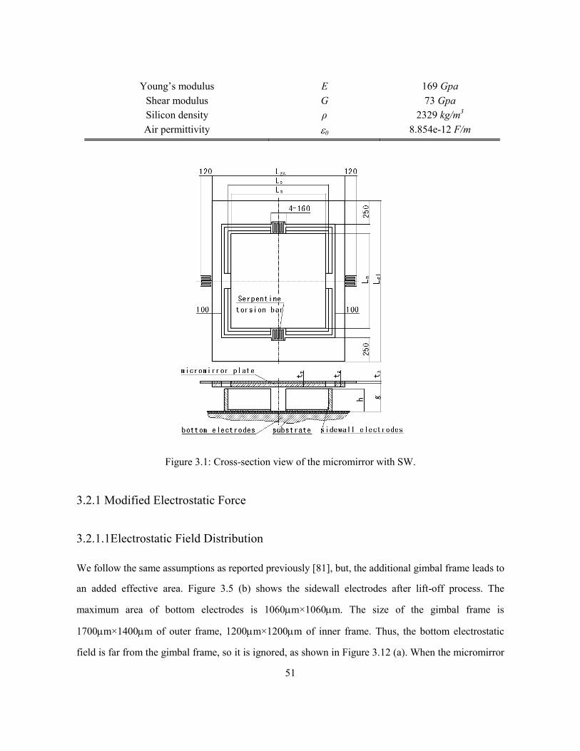
51
Young‘s modulus E 169 Gpa
Shear modulus G 73 Gpa
Silicon density ρ 2329 kg/m3
Air permittivity 0 8.854e-12 F/m
Figure 3.1: Cross-section view of the micromirror with SW.
3.2.1 Modified Electrostatic Force
3.2.1.1Electrostatic Field Distribution
We follow the same assumptions as reported previously [81], but, the additional gimbal frame leads to
an added effective area. Figure 3.5 (b) shows the sidewall electrodes after lift-off process. The
maximum area of bottom electrodes is 1060m×1060m. The size of the gimbal frame is
1700m×1400m of outer frame, 1200m×1200m of inner frame. Thus, the bottom electrostatic
field is far from the gimbal frame, so it is ignored, as shown in Figure 3.12 (a). When the micromirror

52
plate rotates to a large scanning angle, as shown in Figure 3.12 (c), the bottom electrostatic field on
the gimbal frame is still weak and can be ignored as well. Therefore, only the electrostatic force
caused by the sidewall electrodes on the gimbal frame is considered. When calculating the double
integral, the integral domains on the gimbal frame are the entire gimbal frame with edges along the X-
axis.
3.2.1.2 Electrostatic Force on Gimbal Frame
The gimbal frame only can rotate about the -scan axis. The additional moment of electrostatic force
that is contributed from the sidewall electrodes (e12, e22, e32 and e42) on gimbal frame is:
22_12
2
0
22_12
2
2
022_12
2
1
cos2
1)sin(
2
1efg
Se
EgGVdxdy
yLeyVVT
(3.1a)
42_32
2
0
42_32
2
2
042_32
2
1
cos2
1)sin(
2
1efg
Se
EgGVdxdy
yLeyVVT
(3.1b)
Simultaneously, the micromirror plate is pulled down along Z direction, so that the electrostatic
forces caused by the e12, e22, e32 and e42 electrodes on gimbal frame along Z-direction are the sum of
the components: dPe12cos(/2-), dPe22cos(/2-) , dPe32cos(/2-) , and dPe42cos(/2-).
22_12
2
0
2
22_12
2
022_12
2
1
cos2
1)sin()2/cos(
2
1fgZe
Se
ZeEg
GVdxdy
yLeVVF
(3.2a)
42_32
2
0
2
42_32
2
042_32
2
1
cos2
1)sin()2/cos(
2
1fgZe
Se
ZeEg
GVdxdy
yLeVVF
(3.2b)
, where Gfgeij , and GfgZeij are integral factors, and is the maximum slope angle of the mirror to the
sidewall electrode.

53
3.2.1.3 Equilibrium between Electrostatic Force and Mechanical Torsion
When the micromirror plate is actuated by the electrodes, the equations can be derived in terms of the
equilibrium between the electrostatic and mechanical torques,
4
1
2
4
1
3
1 i
ei
Eg
i j
eij
ETTK
(3.3a)
4
1
3
1i jeij
ETK
(3.3b)
4
1
2
4
1
3
1 i
ZeiEg
i j
ZeijE
b FFZK (3.3c)
, where KandKare the torsional stiffness of the 3-end serpentine bar at the and scans,
respectively. Kb is the bending stiffness along Z-direction. We will derive these parameters in the
subsequent section.
3.2.1.4 Dynamic Modeling
The dynamic response of the biaxial micromirror was derived by using the Lagrange Formulation [81,
106, 109]. The air-damping effects can be neglected since the gap between the micromirror plate and
bottom electrodes is about 290m and the micromirror works in the low frequency range (less than
500Hz). Thus, by introducing to the normalized parameters [81], and letting 1x , ddx 2 ,
3x , ddx 4 , Eqs. (2.27) become a first-order differential equation set
2
01
34
43
2
021
12
21
)(
J
Txx
xx
JJ
TTxx
xx
E
EgE
(3.4)

54
(a) (b)
(c) (d)
Figure 3.2: SEM of a single MEMS mirror with sidewall electrodes (micromirror with 1.5m torsion
bar). (a) as-fabricated micromirror with SW; (b) 1.5m 3-end serpentine torsion bar; (c) 1.5m 2-end
serpentine torsion bar; (d) free body diagram of a 3-end serpentine torsion bar.

55
3.2.2 Stiffness of the Serpentine Torsion Bar
In comparison to a straight torsion bar, a serpentine torsion bar provides several advantages by: i)
extending the effective length of beam; ii) minimizing the occupied space in order to deduce the
overall size; and iii) being well-suited for simple bulk micromachining technology. There are three
configurations: classic, 2-end rotated [110, 111], and 3-end serpentine springs. Figure 3.2 (b)
illustrates a 3-end serpentine spring (a guided-end beam with two fixed ends and one end with the
mirror plate). From the structural viewpoint, the 3-end serpentine spring is a more stable structure
than the classic and rotated springs, and we have adopted it here. Although the 3-end serpentine
spring is a statically indeterminate structure, the spring constant can be derived from Castigliano‘s 2nd
theorem and the unit-load method directly [100, 112].
In order to build a stiffness model for the 3-end serpentine spring, we make several reasonable
assumptions, such as small angle and vertical deflections, ignoring residual stress and extensional
stress, adopting the neutral surface as an analysis basis, and considering the 3-end serpentine torsion
bar as a guided-end beam. Meanwhile, we use Fz0, TM0, and M0 to present the forces and torques
caused by the mirror plate, as shown in Figure 3.2 (d). Table 3.2 lists the transferred bending
moments and torques imposed on all 17 segments of the spring, resulting from external electrostatic
loads at the free end, in order to express the total strain energy. In Table 3.2 the variable, represents
the individual local coordinate that is along the axial length direction. Castigliano‘s 2nd
theorem states
that the partial derivative of the strain energy of a linear structure, U, with respect a given load, Fi, Mi,
and Ti, is equal to the displacement at the point of application of the load, i , i and i :
i
iF
U
i
iM
U
i
iT
U
(3.5)
In order to obtain individual spring constants from Eqs. (3.5), we can solve one the expressions and
let the other two deflections equal zero simultaneously. Letting i=0 and i=0, M0 and Fz0 are zero,
and for the torsional deflection, we obtain

56
Table 3.2: Force balance on each segment of the spring (from free end)
Segment
No. Length Moment Torque
1 lf M0+Fz0 TM0
2 lo 1/2TM0+1/2Fz0 1/2M0+1/2Fz0lf
3 lp 1/2M0+1/2Fz0(lf - 1/2TM0+1/2Fz0lo
4 lo 1/2TM0+1/2Fz0(lo+ 1/2M0+1/2Fz0(lf -lp)
5 lp 1/2M0+1/2Fz0(lf -lp+ 1/2TM0+Fz0lo
6 lo 1/2TM0+1/2Fz0(2lo + 1/2M0+1/2Fz0lf
7 lp 1/2M0+1/2Fz0(lf - 1/2TM0+3/2Fz0lo
8 lo 1/2TM0+1/2Fz0(4lo+ 1/2M0+1/2Fz0(lf -lp)
9 li 1/2M0+1/2Fz0(lf -lp+ 1/2TM0+2Fz0lo
10 lo 1/2TM0 -1/2Fz0 1/2M0+1/2Fz0lf
11 lp 1/2M0+1/2Fz0(lf - 1/2TM0 -1/2Fz0lo
12 lo 1/2TM0 -1/2Fz0(lo+ 1/2M0+1/2Fz0(lf -lp)
13 lp 1/2M0+1/2Fz0(lf -lp+ 1/2TM0 -Fz0lo
14 lo 1/2TM0 -1/2Fz0(2lo+ 1/2M0+1/2Fz0lf
15 lp 1/2M0+1/2Fz0(lf - 1/2TM0 -3/2Fz0lo
16 lo 1/2TM0 -1/2Fz0(3lo+ 1/2M0+1/2Fz0(lf -lp)
17 li 1/2M0+1/2Fz0(lf -lp+ 1/2TM0 -2Fz0lo
b
o
t
ipf
MtEI
l
GJ
lll
T
84
12
4
16
4
1
0
(3.6)
Letting i=0, TM0 is zero, such that for the bending moment stiffness Kand the bending force
stiffness KF, we obtain
opofpf
t
iipifppff
b
Z
op
t
ipf
b
b
llllllGJ
lllllllllEI
F
llGJ
lllEI
M
474
1
222624
1
74
1264
4
1
222
0
0
(3.7)

57
ioopfpoof
t
iippf
ippfppfpfof
b
opof
t
ipipifpff
b
b
lllllllllGJ
lllll
lllllllllll
EIF
llllGJ
lllllllllEI
M
2222
322
232233
0
222
0
3242844
1
3
1
223
642
3
1
4
1
284
1
2
1
2
332
2
1
4
1
(3.8)
Eqs.(3.7) and (3.8) can briefly be written as the following simplified forms:
022021
012011
Zb
Zb
FCMC
FCMC
(3.9)
, where the coefficients C11, C12, C21, and C22 are the terms of flexibility matrix of the spring. Thus, in
terms of the definition of spring constant [112], the torsion stiffness Kt for a side spring is given by:
1
84
12
4
16
4
1
b
o
t
ipf
tEI
l
GJ
lll
K (3.10)
Meanwhile, due to rigid body assumption of the micromirror with SW, no bending slope at free end
of the serpentine spring is expected where there is a joint between the spring and the micromirror.
This boundary condition is satisfied by letting the first equation in (3.9) equal zero at the joint.
Substitution of the solved equivalent bending moment into the second equation in (3.9) gives the
bending stiffness at the free end:
21122211
11
CCCC
CK
b
(3.11)
The rotational stiffness at the free end can be

58
21122211
22
CCCC
CK
b
(3.12)
Thus, we deduced the spring constant coefficient for one side of serpentine bar. For two sides of the
serpentine bars, we only need to double the coefficients.
3.3 Fabrication Process
The fabrication process is divided into three steps: (i) micromirror plate fabrication, (ii) sidewall
electrode fabrication, and (iii) assembly of the micromirror plate and sidewall electrodes. Single
micromirror with SW, 2×2 micromirror array with SW and 4×4 micromirror array with SW are
fabricated through this process.
3.3.1 Micromirror Plate Fabrication
The micromirror plate is fabricated on an SOI wafer. The SOI wafer is 100mm, device layer 12m,
buried oxide layer 0.5m and handle layer 290m. The fabrication process, shown in Figure 3.3, is
based on reactive ion etching (RIE) and high aspect ratio deep reactive ion etching (DRIE).
Fabrication of the front side features: Layers of 0.5m and 2m silicon dioxide are deposited by
using plasma enhanced chemical vapor deposition (PECVD) on top of the device layer and the handle
wafer layer, respectively. Photoresist (PR) is patterned on the device layer to define the mirror plate
features. RIE follows next to etch the 0.5m silicon dioxide layer. The patterned silicon dioxide layer
is used as a mask for the subsequent DRIE process. Next, Bosch Etching DRIE is used to etch silicon
and stopping on the buried oxide layer. This process forms the tiny serpentine torsion bars, the mirror
plate and the gimbal frame on the device layer, as shown in Figures 3.3 (a)~(c).
Fabrication of the back side features: PR is patterned on the handle wafer layer to define the back
features of the mirror. RIE is used to etch the 2m silicon dioxide layer to expose the silicon, as
shown in Figure 3.3 (d). PR is patterned on the exposed silicon to define the backside patterns of the
micromirror plate and the gimbal frame, as shown in Figure 3.3 (e). DRIE is used to etch the exposed
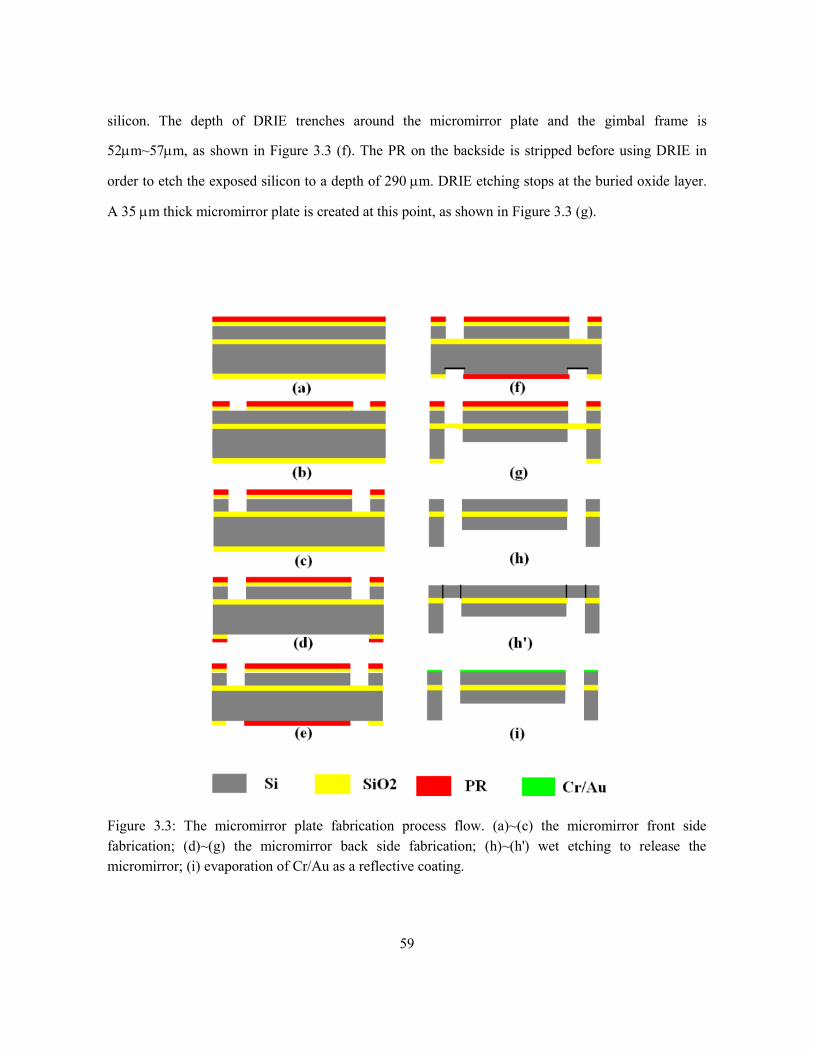
59
silicon. The depth of DRIE trenches around the micromirror plate and the gimbal frame is
52m~57m, as shown in Figure 3.3 (f). The PR on the backside is stripped before using DRIE in
order to etch the exposed silicon to a depth of 290m. DRIE etching stops at the buried oxide layer.
A 35m thick micromirror plate is created at this point, as shown in Figure 3.3 (g).
Figure 3.3: The micromirror plate fabrication process flow. (a)~(c) the micromirror front side
fabrication; (d)~(g) the micromirror back side fabrication; (h)~(h') wet etching to release the
micromirror; (i) evaporation of Cr/Au as a reflective coating.

60
Release of the micromirror plate from the SOI wafer: Releasing the micromirror plate is a
challenge in the fabrication process. A wet etching method is adopted to release the micromirror plate
by using 6:1 Buffered Oxide Etchant (BOE). After releasing the micromirror from the SOI wafer, DI
water cleans the surface and pure alcohol dries it, as shown in Figure 3.3 (h). Figure 3.3 (h') shows the
cross-sectional view of the device when rotated by 90º.
Evaporation of the reflective metals: Cr or Ti (16nm) is evaporated by using a CVC4500
evaporator as an adhesive layer before evaporating Au (150nm) as the reflective surface. Figure 3.3 (i)
shows this process. The thickness of the reflective thin film affects the micromirror curvature, while
the thin film quality influences the surface reflectivity.
3.3.2 Sidewall Electrodes Fabrication
The sidewall electrodes are fabricated on another SOI wafer, diameter 100mm, with device layer
250m, buried oxide layer 2m and handle layer 300m. There are two challenges in this: (i)
fabricating the 250m tall sidewall electrodes on the SOI wafer; and (ii) patterning the connecting
wire and pad on the bottom and sidewall electrodes. For the high aspect ratio structure, it is
impossible to pattern through PR and evaporate metal layers on the vertical surface. Thus, a high
aspect ratio shadow mask and bulk sidewall electrode fabrication are used to form the sidewall
electrodes.
Fabrication of the shadow mask: The shadow mask is fabricated by a single crystal silicon (SCS)
based on bulk micromachining technique. The SCS wafer has a diameter 100mm with thickness
250m. RIE and DRIE are used to pattern the shadow mask features.
Fabrication of the bulk sidewall electrode: A 2.5m silicon dioxide layer is deposited by using
PECVD on top of the device layer. Subsequently, a thicker PR (S1845) is patterned on top of the
silicon dioxide layer. Next, RIE is used to etch the 2.5m silicon dioxide layer. Finally, the structure
of bulk sidewall electrodes is obtained by DRIE. The process is shown in Figures 3.4 (a)~(c).

61
Figure 3.4: The sidewall electrodes fabrication process flow. (a)~(c) sidewall electrode fabrication by
DRIE; (d)~(e) assembly of shadow mask and evaporation of metal Cr/Al as a conductive layer; (f)
lift-off of the shadow mask to obtain the sidewall electrodes.
Assembly of a shadow mask on the sidewall electrodes: Figure 3.4 (d) and Figure 3.5 (a) present the
assembling of a shadow mask on the sidewall electrode wafer. Cr or Ti (16nm) as an adhesive layer
and Al layer (1~1.2m) are sputtered on the sidewall surface by using CVC Sputter Dep System.
Figure 3.4 (e) shows the process. Finally, the shadow mask is removed by a lift-off process, shown in
Figure 3.4 (f), and then the sidewall wafer is diced into single dies. Figure 3.5 (b) shows the pattern
on the sidewall electrodes after lift-off the shadow mask.
3.3.3 Assembly of the Micromirror Plate and SW Electrodes
The last step is to assemble the micromirror plate and sidewall electrodes through using a transparent
alignment tool built on a Pyrex glass wafer with four pins (height 50m) and the HTG System III-HR
Contact Aligner (HTG). The assembly process resembles flip-chip method. The die of the sidewall

62
(a)
(b)
Figure 3.5: SEM of the sidewall electrodes. (a) assembly of the shadow mask and the sidewall
electrode wafer; (b) the sidewall electrodes after shadow mask lift-off.

63
electrodes with a small quantity of epoxy glue, SU-8, is putted on top of HTG stage, and then the
micromirror plate is stacked and aligned on the sidewall electrodes. Applied low pressure through the
alignment tool, the micromirror plate is glued to the sidewall electrodes. Subsequently, the
micromirror device is placed in a 90oC
oven for 12 h. Figure 3.2 (a) shows the single micromirror
with SW.
The yield rate is about 80% for the single micromirror with SW. The micromirrors are needed to
store in a drying environment to keep Cr/Au reflective layer drying and clean.
3.4 Simulation and Experiment
Two types of micromirrors with SW having 3m and 1.5m torsion bars are fabricated at the Cornell
Nanoscale & Sciences Facility (CNF). One micromirror without SW (only bottom electrodes), and
having 3m torsion bar and identical mirror parameters is also fabricated. Extensive experiments are
performed to investigate the static and dynamic characteristics of the micromirror and verify the
analytical modeling.
3.4.1 Experiment Configuration
The micromirror is driven by a differential drive method in order to obtain scan linearity [15]. The
micromirror plate and the gimbal frame are electrically grounded. The drive voltages on the quadrant
electrodes (sidewall and bottom electrodes) are denoted by V1, V2, V3 and V4. The differential drive
voltages are defined in Eq. (2.17).
In the experiment configuration, the MEMS mirror is controlled by signals generated by LabVIEW.
A position sensitive detector (PSD) is used to measure the position of a laser spot reflected by the
MEMS mirror. A data acquisition (DAQ) system is used to record the experimental data. Figure 3.6
shows the schematic experiment configuration.

64
Figure 3.6: Schematic experimental configuration for characterizing the micromirror.
3.4.2 Static Characteristics
Only one quadrant of the micromirror is investigated because of the symmetry of the structure. Figure
3.7 illustrates the analytical modeling and experiment results for the static properties of the
micromirror with 3m torsion bar. Figure 3.8 shows the micromirror with 1.5 m torsion bar. For the
case of the micromirror with 3m torsion bar, as shown in Figure 3.7, the Vbias is 55V, and Vx and Vy
range from 0 to 100V. When Vx and Vy are 100V, the scan angular deflection is about 0.80o and
0.87o, respectively, as shown in Figures 3.7 (a) and (c). The scan is 0.61
o and 0.68
o, respectively, as
shown in Figures 3.7 (b) and (d). For the case of the micromirror with 1.5m torsion bar, Vbias is 55V,
and Vx and Vy range from 0 to 30V. When Vx and Vy are 25V, the scan angular deflection is about
1.71o and 2.68
o, respectively, as shown in Figures 3.8 (a) and (c), while the scan is about 1.31
o and
1.42o, as shown in Figures 3.8 (b) and (d).
From Figures 3.7-3.8, it is observed that: i) there is a good linearity under small scanning angles,
with good-consistency between the analytical modeling and experimental results; ii) the mirror with
3m torsion bar reaches a small angle under the differential voltage 100V, but the mirror with 1.5m
torsion bar achieves a large angle under 25V and the stiffness of spring constants affects the behavior
of the mirror greatly.

65
(a) (b)
(c) (d)
Figure 3.7: The linearity of the scanning angle and drive voltage for the micromirror with 3m
serpentine torsion bar. (a) -scan angle displacement (from models); (b) -scan angle displacement
(from models); (c) -scan angle displacement (from experiments); (d) -scan angle displacement
(from experiments).
(deg
ree)
(deg
ree)
(deg
ree)
(deg
ree)

66
(a) (b)
(c) (d)
Figure 3.8: The linearity of the scanning angle and drive voltage for the micromirror with 1.5m
serpentine torsion bar. (a) -scan angle displacement (from models); (b) -scan angle displacement
(from models); (c) -scan angle displacement (from experiments); (d) -scan angle displacement
(from experiments).
(deg
ree)
(deg
ree)
(deg
ree)
(deg
ree)
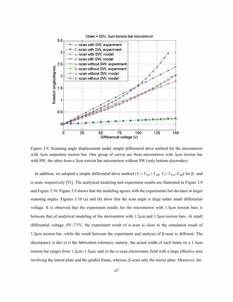
67
Figure 3.9: Scanning angle displacement under simple differential drive method for the micromirror
with 3m serpentine torsion bar. One group of curves are from micromirror with 3m torsion bar
with SW, the other from a 3m torsion bar micromirror without SW (only bottom electrodes).
In addition, we adopted a simple differential drive method (V1=Vbias+Vdiff, V2=Vbias-Vdiff) for - and
-scan, respectively [91]. The analytical modeling and experiment results are illustrated in Figure 3.9
and Figure 3.10. Figure 3.9 shows that the modeling agrees with the experiments but deviates at larger
scanning angles. Figures 3.10 (a) and (b) show that the scan angle is large under small differential
voltage. It is observed that the experiment results for the micromirror with 1.5m torsion bars is
between that of analytical modeling of the micromirror with 1.2m and 1.5m torsion bars. At small
differential voltage, 0V~7.5V, the experiment result of -scan is close to the simulation result of
1.2m torsion bar, while the result between the experiment and analysis of -scan is different. The
discrepancy is due to i) the fabrication tolerance, namely, the actual width of each beam on a 1.5m
torsion bar ranges from 1.2m~1.5m, and ii) the -scan electrostatic field with a large effective area
involving the mirror plate and the gimbal frame, whereas, -scan only the mirror plate. Moreover, the

68
(a)
(b)
Figure 3.10: Scanning angle displacement under simple differential drive method. The micromirror
with SW is based on different widths of torsion bar, 1.2m, 1.5m, and 2m. The micromirror
without SW is based on 1.5m and 2m width torsion bars. (a) -scan angle displacement; (b) -scan
angle displacement.

69
effects of the spring stiffness nonlinearity become larger along with increasing the scanning angle.
However, although there are deviations at large scanning angle as shown in Figures 3.9-3.10, the
analytical modeling is adequate for estimating the static characteristics of the micromirror with small
angular deflection. Therefore, the analytical model can be used for determining the required
micromirror parameters before an expensive fabrication run. Meanwhile, in comparison to the
micromirror with only bottom electrodes, the micromirror with SW has demonstrated to achieve a
larger scan angle for using the same drive voltage.
Pull-in properties: Figure 3.11 shows the large angular deflection for the micromirrors with 3m 3-
end torsion bars and 1.5 m 2-end serpentine bars. Figure 3.2 (c) shows the 2-end serpentine bar (a
guided-end beam with one fixed end and one end with the mirror plate). In Figure 3.11 (a), the -scan
angular deflection of the mcromirror with 3m 3-end torsion bar has three phases: 0o~4.5
o, 4.5
o~6.5
o,
6.5o~11
o. In Figure 3.11 (b), for -scan, the pull-in can be observed when the mcromirror rotates
about 5.5o. Such results are caused by the changes of electrostatic field distribution and the spring
stiffness of different torsion bars. Figure 3.12 shows the changes of electrostatic field distribution
under different -scan deflection. The -scan has a similar distribution, but without the gimbal frame.
When the mirror plate rotates to 1 (around 5.5o), the edge of the mirror plate is closest to the
sidewall, as shown in Figure 3.12 (b). In this condition, the fringe field generates a maximum bending
moment, Mo, to pull the mirror plate closer to the sidewall. Thus, the narrower the width of torsion
bars, the smaller is the spring stiffness and thereby, the larger the lateral shift.
The experimental results in Figure 3.11 (b) have a convex shape because: i) the sidewall
electrostatic field and fringe field can prevent the spring-softening effect [20]; and ii) the spring
stiffness of the 1.5m 2-end serpentine torsion bar has nonlinear property under large angular
deflection. The width of a torsion bar affects both the ratio and linearity of the voltage-to-angle
relationship. A smaller torsion bar width will decrease the required drive voltage to achieve a large
angular rotation, however, it will also induce nonlinearity in the relationship.

70
(a)
(b)
Figure 3.11: Large scan angle tests with simple differential drive method at- and - scan. (a)
micromirror with 3m 3-end torsion bar with SW, Vbias = 55V; (b) micromirror with 1.5m 2-end
serpentine bar with SW, Vbias=18V.

71
Figure 3.12: Electrostatic field distribution of one quadrant of the micromirror with SW under
different angular deflection. (a) scanning angle 0o ; (b) scanning angle 1 ; (c) scanning angle 2 .
3.4.3 Dynamic Characteristics
There are two important characteristics of the dynamic properties of the micromirror: (i) the
resonance frequency and (ii) resonance frequency shifting.
3.4.3.1 Resonance Frequency of the Micromirror
The dynamic response of the micromirror can be solved by through Eq. (3.6). To simulate the
response of the micromirror, the following arbitrary initial values were assumed: [x10,x2
0,x3
0,x4
0]=[0,
0.012, 0, 0.02]. Eq. (3.4) can be solved by the Runge-Kutta method [81], to obtain the periods, T and
T, and thereby the resonant frequency, under different bias voltages, f and f (Tff) [81].
In order to find the system resonance frequency experimentally, the micromirror is actuated by DC
and AC voltages. The sinusoidal AC voltage has a frequency range of 1- 1000Hz. The peak voltages
show the resonant frequency response of the scan and scan, as shown in Figure 3.13. Thus, the

72
(a)
(b)
Figure 3.13: The frequency response of micromirror with 3m torsion bar and 1.5m torsion bar
under sinusoidal sweep experiments for a frequency range of 1Hz to 1000Hz. (a) Micromirror with
3m torsion bar; (b) Micromirror with 1.5m torsion bar.

73
resonance frequency under different DC bias voltage is tested. The micromirror with 3m 3-end
torsion bar has the resonance frequency 454.6Hz at -scan, 215.4Hz at -scan, the micromirror with
1.5m 3-end torsion bar has the resonance frequency 146.5Hz at -scan, 50.2Hz at -scan, under DC
bias voltage 55V. In addition, for one micromirror with 3m torsion bars running at the resonance
frequency, the scanning angle reaches ±12º (mechanical angle, Vbias=55V Vac=35V, fr=181Hz) at -
scan, and ±20º (mechanical angle, Vbias=80V Vac=80V, fr=383Hz) at -scan.
3.4.3.2 Resonance Frequency Shifting
The resonant frequency changes under different bias voltages [96]. This is an important property of
MEMS mirrors actuated by electrostatic forces. The resonance frequency determines the scanning
frequency bandwidth of the micromirror. The larger the resonance frequency shifting, the smaller is
the bandwidth. It is known that micromirrors without SW have large range resonance frequency shifts.
However, although the micromirror with SW still exhibits this phenomenon, it is much smaller, i.e.
the sidewall electrodes suppress resonance frequency shifting, in that the fringe field effects from
sidewall electrodes affect the stiffness of the tiny torsion bars. Figure 3.14 illustrates this under
different bias voltages, showing good agreement between ANSYS simulation and experiments in
terms of the values of Table 3.3. In addition, from the dynamic tests for the micromirror without SW,
the resonance frequency shifting cannot be observed: the reason is the large gap between the mirror
plate and bottom electrodes, around 300m. The generated electrostatic force is small and has very
weak contribution for changing the resonance frequency through different bias voltages.
In fact, the resonance frequency under different bias voltages can be obtained by solving Eq. (3.4).
It also indicates that the resonance frequency shift is negligible. Figure 3.15 shows the 3-D profile of
the mirror with SW that was acquired from the Olympus LEXT OLS3100 confocal microscope. The
height between the mirror plate and the edge top of the sidewall electrodes is about 55m. However,
in the analytical models, we assume that the effective integral domain is enclosed by the micromirror
edges and the projected lines of the lower sidewall electrostatic field [76], and ignore upper sidewall

74
(a)
(b)
Figure 3.14: The resonance frequency shifting under different bias voltages (ANSYS and
experiments). (a) Resonance frequency shifting of -scan; (b) Resonance frequency shifting of -scan.

75
Table 3.3: α-scan and β-scan resonance frequency values under different bias voltages
Bias
voltage
(V)
Micromirror with 3m width torsion bars Micromirror with 1.5m width torsion bars
α-scan, resonance frequency(Hz)
(mirror plate with gimbal frame)
β-scan, resonance frequency(Hz)
(mirror plate)
α-scan, resonance frequency(Hz)
(mirror plate with gimbal frame)
β-scan, resonance frequency(Hz)
(mirror plate)
Experiment ANSYS Experiment ANSYS Experiment ANSYS Experiment ANSYS
10 224.2 247.4 462.8 584.9 75 82.7 176.8 203.5
20 222.9 246.6 461.9 584.0 72.2 80.5 173.5 201.0
30 221.5 245.3 460.5 582.6 68.8 76.7 168.8 196.7
35 220.5 244.5 459.6 581.6 66.2 74.2 166.2 193.8
40 219.4 243.5 458.7 580.5 64.2 71.1 163.3 190.4
45 218.1 242.4 457.7 579.2 61.3 67.4 156 186.6
50 216.6 241.5 456.5 577.8 58.7 63.1 151.5 182.1
55 215.4 239.7 454.6 576.2 50.2 57.9 146.5 177.1
60 213.5 238.2 453 574.5 45.8 51.7 140.4 171.4

76
Figure 3.15: 3D profile of the mirror with SW acquired from an Olympus LEXT OLS3100 confocal
microscope, and the distance between the mirror plate and the top of sidewall electrodes.
electrostatic field and fringe field effects. This assumption is a major contributor to the differences
among the analytical modeling, experiments, and ANSYS simulation.
In addition, the ANSYS simulation results are larger than the measurements. These differences are
attributed to discrepancies in the estimation of material parameters and fabrication tolerance.
3.5 Conclusions
In terms of both the analytical modeling and the experiments, the characteristics of the MEMS
micromirror with SW are determined by several factors: the cross section (width and thickness) and
length of the serpentine torsion bars, the distance between the mirror plate and bottom electrodes, and
the height of sidewall electrodes. The higher the sidewall electrodes, the smaller are the electrostatic

77
field effects of the bottom electrodes and the smaller the resonance frequency shifting. Within a small
scanning angle range, the mirror scan is linear under differential voltage drive, but, as the scanning
angle is increased, nonlinearity is observed. Although there are differences between the analytical
models and the experiments, they are very consistent at small scanning angles. In this domain, the
analytical modeling describes the system very well and can be used as a very good reference during
the design phases before a commitment to a fabrication runs. It is also shown that the height of the
sidewall electrode affects the pull-in threshold during the large angular deflection.
3.6 Summary
A novel biaxial MEMS mirror with SW electrodes has been fabricated successfully in terms of a new
fabrication process. The static and dynamic characteristics of the micromirror with SW electrodes are
obtained. In the following chapters, the extended fabrication process succeeds in achieving
micromirror arrays, and also a biaxial MEMS mirror with SW electrodes is used into a laser scanning
microscope system – the MACROscope system.
78
Chapter 4
Design and Fabrication of 2×2 and 4×4
Micromirror Array
4.1 Introduction
2×2 and 4×4 micromirror arrays based on the extended fabrication process are fabricated in order to
get a large optical aperture that is the requirement of the EOCT and confocal microscope for
obtaining high resolution images [67]. The optical aperture is determined by a micromirror plate.
However, the larger the micromirror plate, the lower resonance frequency the micromirror has. To
simulate a large aperture tilt micromirror, micromirror arrays divide a large aperture into small
micromirrors with significantly reduced inertia and increase rotation speed. Different types of
micromirror arrays apply to optical switches, DMD, adoptive optics (AO) [3], telescope [114, 115],
and optical phased arrays [116, 117]. DMD developed by Texas Instrument Inc is widely adopted into
digital light projector (DLP) and confocal microscopy [118]. Each mirror in DMD is only 10m or a
little bit large with ―on‖ or ―off‖ state. Optical phased array technology was developed by Paul F.
McManamon et al. [119]. Micromirror arrays can be used as optical phased arrays for laser beam
steering. Several types of micromirror arrays are fabricated in terms of surface micromachining or
hybrid bulk/surface micromachining techniques [12, 22, 114-117, 120]. Micromirror arrays process
several advantages: low inertia, high frequency, and large field of view (FOV). Therefore, applying a
micromirror array to Endoscopic OCT and confocal microscope becomes the motivation of design

79
(a)
(b)
(c)
Figure 4.1: The structure of 2×2 micromirror array. (a) schematic of one micromirror element; (b)
overview of 2×2 micromirror array; (c) close-up view of one micromirror on the right corner.

80
and fabrication of 2×2 and 4×4 micromirror arrays.
This chapter presents the design and fabrication of 2×2 and 4×4 micromirror array. Although the
process flow of micromirror arrays is based on that of the single micromirror with SW electrodes [82],
relevant modification and plenty of optimization on the mirror array design and fabrication
parameters are required.
4.2 Design of Micromirror Arrays
The schematic design of 2×2 micromirror array is shown in Figure 4.1. The micromirror array is
composed of a mirror plate array and sidewall electrodes. The size of one mirror plate in the array is
1mm×1mm, which is supported by two pairs of 3-end serpentine torsion bars, and the total optical
aperture combined from four micromirrors is close to 2mm×2mm. The gap between the mirror plate
array and bottom electrodes is about 300m, which makes each micromirror have a large scan angle
potentially. The width of the torsion bar is designed to 2m. Figure 4.1 (a) illustrates a cross–view of
one micromirror, and Figure 4.1 (c) shows a close–up view on the right corner micromirror. Figures
4.3 (b) and (c) show outer and inner 3-end serpentine torsion bars. In order to control each
micromirror, the mirror plate array is an electrical ground and each cell of 2×2 SW electrode actuators
is insulated. The driving voltages, V1,V2, V3 and V4, are added onto each actuator, respectively. Figure
4.3 illustrates 2×2 micromirror array bonded in a chip carrier. In addition, the fill factor is an
important parameter for micromirror array devices. Fill factor can be calculated through equation
[117]:
2
ba
af
(4.1)
in which a is the size of each sub-aperture, and b is the spacing between adjacent pixels. Due to the
electrostatic actuators, a can be in millimeter scale. The choice of b is subjected to several factors
including the robustness of the silicon walls, manufacturability and process tolerances. In a 2×2

81
micromirror array, a=1mm and b=335μm, rendering a fill factor of 56%. However, for a 4×4
micromirror array, a=1mm and b=1.4mm, rendering a fill factor of 17%.
4.3 Fabrication of 2×2 Micromirror Array
The fabrication process of 2×2 micromirror array is based on that of the single micromirror with SW
electrodes and is composed of micromirror array fabrication, SW electrode fabrication, and assembly
of micromirror array and SW electrodes. This section emphasizes the fabrication process specialties
and difference between single micromirrors and micromirror arrays.
4.3.1 Micromirror Array Fabrication
The micromirror array is built on a double side polished (DSP) SOI wafer, 100mm diameter, with
12m device layer, 0.5m buried oxide layer, and 290m handle layer. The process, as shown in
Figure 4.2, is based on reactive ion etching (RIE) and high aspect ratio deep reactive ion etching
(DRIE).
Shallow trench etched on top of the handle layer: A layer of 0.5m silicon dioxide (SiO2) is
deposited by GSI PECVD on top of the device layer. S1818 Photoresist (PR) is patterned on top of
the handle layer to define a shallow trench area. Bosch Etching DRIE follows next to etch the shallow
trench, depth 8-9m. The first depth is created, as shown in Figures 4.2 (a) and (b). Then, the
remained PR is cleaned by Hot Tank. A layer of 2m SiO2 is deposited by GSI PECVD on top of the
fabricated handle layer, as shown in Figure 4.2 (c).
2×2 micromirror array patterned on top of the device layer: S1813 PR is patterned on the device
layer. RIE is used to etch SiO2 as a mask for the next DRIE etching. DRIE etching silicon stops on
the buried oxide layer. This process forms tiny serpentine torsion bars, the mirror array and the
gimbal frame on the device layer, as shown in Figures 4.2 (d) and (e). The diagrams in Figure 4.3
show the pattern of 2×2 micromirror array.

82
Figure 4.2: The fabrication process flow of 2×2 and 4×4 micromirror arrays
Backside features of 2×2 micromirror array etched on top of the handle layer: Subsequently,
S1818 PR is patterned on the handle layer to define backside features of the micromirror array. RIE is
used to etch the 2m silicon dioxide layer to expose the silicon handle layer, as shown in Figure 4.2
(f). PR is patterned on the exposed silicon to define the backside patterns of the micromirror array and
the gimbal frame, as shown in Figure 4.2 (g). DRIE is used to etch the silicon on the backside. The
depth of the DRIE trenches around the mirror array and the gimbal frame is 60-65m, as shown in
Figure 4.2(h). PR on the backside is stripped and then DRIE is used to etch the exposed silicon to a
depth of 290m, as shown in Figure 4.2 (i). The backside features of 2×2 micromirror array after
DRIE etching is illustrated in Figure 4.4. DRIE etching stops at the buried oxide layer. A 35m thick
micromirror plate is created at this point. As shown in Figure 4.4 (c), four layers on the backside are
created from three masks. In terms of the literatures, the maximum layers are three, and it is the first

83
time to get four layers through DRIE for fabricating complex structures. After DRIE etching, the
buried oxide layer is exposed and shown in Figure 4.5. The thermal SiO2 layer is a compressive
unstressed layer. After exposed, it becomes a buckled thin film, as shown in Figure 4.5(b). The tiny
serpentine torsion bars will be damaged if the deformation of the thin film is too big. This effect has
to be considered when designing 3-end serpentine torsion bars.
(a)
(b) (c)
Figure 4.3: The front side features and critical 3-end serpentine torsion bars. (a) SEM of 2×2
micromirror array; (b) outer serpentine torsion bar; (c) inner serpentine torsion bar.

84
(a)
(b) (c)
Figure 4.4: The backside features of the micromirror array plate after DRIE. (a) SEM of the backside
feature of the micromirror array plate; (b) close-up view of the backside gimbal frame and mirror
plate on the serpentine torsion bar area; (c) overview of the corner on the mirror plate backside.

85
(a)
(b)
Figure 4.5: The compressive unstressed SiO2 thin film exposed after DRIE. (a) backside view on the
serpentine torsion bar area; (b) frontside view close to serpentine torsion bars.
Release of the micromirror plate array: The micromirror array is released by a wet etching method.
6:1 Buffered Oxide Etchant (BOE) is adopted. After releasing the micromirror array from the SOI
wafer, DI water and pure alcohol are used to dry the surface, as shown in Figure 4.2 (j). Figure 4.2 (j')
shows the cross-sectional view of the device when rotated by 90o.

86
Evaporation of the reflective metal layer: The subsequent step is to evaporate the reflective metals,
for which Cr or Ti (16nm) is evaporated by a CVC4500 evaporator as an adhesive layer, and then Au
(150nm) as a reflective surface. Figure 4.2 (k) shows this process. The thickness of the reflective thin
film affects the micromirror curvature, while the thin film quality influences the surface reflectivity.
4.3.2 Sidewall Electrode Fabrication
The sidewall electrodes are fabricated on another SOI wafer, diameter 100mm, with 250m device
layer, 2m buried oxide layer and 300m handle layer. RIE and DRIE are adopted to form the
sidewall features. The layer of 2.5m silicon dioxide is deposited by PECVD on top of the device
layer, and then, a thicker PR (S1845) is patterned on top of the SiO2 layer to pattern the sidewall
features. Next, RIE is used to etch the 2.5m SiO2 layer. Finally, the bulk sidewall electrode with
250m height is obtained by DRIE. The process is shown in Figures 3.4 (a)~(c). Figure 4.8 (a) shows
the bulk sidewall electrodes after DRIE etching.
In order to get bulk sidewall electrodes, sacrificial walls are designed to enclose the sidewall. After
a long time DRIE, the etch rate is faster at three-fourth position of the entire wafer than at the center
and the edge. There exists a 10-20m difference in the etched depth on the whole wafer. Moreover,
the feature density on the wafer affects DRIE etch rate. The diagrams in Figures 4.8 (b) and (c)
illustrate that the difference of etch rate affects final structure pattern. At the high density area does
the undercut show up while vertical walls at the low density area.
A shadow mask is adopted to pattern wires, pads, and bottom electrode features on the high-aspect-
ratio bulk sidewall electrodes. The shadow mask is fabricated on single crystal silicon (SCS),
diameter 100mm, thickness 250m and 285m. Although a silicon shadow mask has been reported in
[121], the characteristics of the shadow mask for the bulk sidewall electrodes are thicker and applied
on top of the wafer with high-aspect-ratio bulk features. RIE and DRIE are used to pattern the shadow
mask features. Two methods are adopted during the fabrication, as shown in Figure 4.6 and Figure 4.7.
Figure 4.6 shows a dry etching process flow with RIE and DRIE. Figure 4.7 shows a hybrid wet
etching and dry etching process flow. The big difference between two methods is to get different

87
thickness of shadow masks. Dry etching process, Method I, adopts a 250m or 285m DSP SCS
wafer. If fabricating a thinner shadow mask, the thin silicon wafer is expensive and maybe required to
grind to expected thickness. Method II shows a little bit complex process, based on 500m SSP SCS
wafer, but the thickness can be fabricated thinner than 20m.
Subsequently, the shadow mask is assembled on the sidewall electrodes. The HTG System III-HR
Contact Aligner (HTG) is used to align the shadow mask with the sidewall electrodes wafer, as shown
in Figure 3.4 (d). Cr or Ti (16nm) as an adhesive layer and Al layer (1~1.2m) are sputtered on the
sidewall surface by CVC Sputter Dep System. Figure 3.4 (e) shows the process. Finally, the shadow
mask is removed by a lift-off process and the sidewall wafer is cut into single dies. The process is
shown in Figure 3.4 (f).
Figure 4.6: The fabrication process flow of shadow mask based on dry etching (method I)

88
Figure 4.7: The fabrication process flow of shadow mask based on hybrid wet etching and dry etching
(method II)
4.3.3 Assembly of Micromirror Array and SW Electrodes
The last step is to assemble the micromirror array and SW electrodes through a transparent alignment
tool with four pins and HTG contact aligner. A few droplets of epoxy glue, SU-8, are deposited on the
SW electrode die, and then the micromirror array is stacked on top. Subsequently, the micromirror
array with SW electrodes is moved to HTG stage. The micromirror array could be aligned with the
SW electrodes. Figure 4.9 shows an alignment mark on the SW electrodes. With low pressure applied
through the alignment tool, the micromirror plate is glued to the sidewall electrodes. Finally, the
micromirror device is placed in a 90oC
oven for 12 h. The yield rate of 2×2 micromirror array is about
60% after all the process. The 2×2 micromirror array with SW is shown in Figure 4.10.

89
(a)
(b) (c)
Figure 4.8: The bulk sidewall electrodes after fabrication process. (a) SEM of 2×2 sidewall electrode
array; (b) SEM of the bulk sidewall electrodes at the center; (c) SEM of the bulk sidewall electrode at
the corner.

90
Figure 4.9: SEM of alignment mark on the SW electrodes
Figure 4.10: Photograph of 2×2 micromirror array after wire bonding in a chip carrier.

91
4.4 Fabrication of 4×4 Micromirror Array
The design of 4×4 micromirror array has a gimbal structure to realize a biaxial rotation. Each of
micromirrors has the same structure as the single micromirror with SW electrodes developed in
Chapter 3. The micromirror plate is ground electrically, and V1,V2,V3 and V4 are applied on four
sidewall electrodes, respectively. Each micromirror can be controlled separately. The process of 4×4
micromirror array is developed in terms of that of 2×2 micromirror array. The process includes: i)
4×4 micromirror array fabrication; ii) 4×4 sidewall electrode fabrication; iii) assembly of mirror plate
and SW electrodes. The diagrams in Figure 4.11 show 4×4 micromirror array. Figure 4.11 (e) shows
one single micromirror with a broken torsion bar. Although the backside features have been designed,
they are etched out after a long time DRIE due to the large open cavity on the backside of the mirror
plate array. The thickness of the micromirror is 12m without backside features after the entire
fabrication process.
(a) (b)

92
(c) (d)
(e)
Figure 4.11: (a) Assemly of 4×4 micromirror array and SW electrodes; (b) SEM of 4×4 micromirror
array; (c) SEM of SW electrode array; (d) 4×4 SW electrodes after shadow mask lift-off; (e) SEM of
single micromirror with a broken serpentine torsion bar.
4.5 Optimization of Design and Fabrication
The fabrication process of micromirror arrays is more complicated than that of the single micromirror
with SW electrodes. It is a continuous and repeated procedure to optimize the structure design and the
process flow. Several aspects have to be considered. First of all, Bosch DRIE etch rate is effected by
the following: i) aspect ratio of each feature; ii) density of features in one die; iii) open area in one die;
iv) position of one die on the entire wafer. When adopting DRIE etching process, the distribution of

93
DRIE etch rate is faster at three-fourth circle than at the center and the edge of the entire wafer.
Secondly, the structure design has to be optimized in terms of the distribution of DRIE etch rate on
the entire wafer. The dimensions of torsion bars, gimbal frame, and trench not only satisfy mechanical
requirements, but also coincide with the DRIE etch rate. Some sacrificial structures are required in
order to fabricate sophisticate features. Thirdly, assembly of the mirror plate array and SW electrodes
is a challenge. The special alignment mark and transparent alignment tools are important and can be
optimized in the future.
The micromirror array with SW electrodes has a low fill factor. It is possible to improve if the
micromirror plate with a pedestal is mounted on top of the micromirror array with SW electrode. The
following provides a possible process flow: i) fabricating the micromirror plate array with pedestal on
SOI wafer I; ii) fabricating the micromirror array with serpentine torsion bars on SOI wafer II, as
shown in Figure 4.2 (a) to (e); iii) flip-chip bonding the wafer I that includes the micromirror plate
array on top of the wafer II that have serpentine torsion bars and mirror features; iv) removing the
handle layer from the wafer I; v) keeping on following the process in Figure 4.2 (f) to (j‘); vi)
evaporate Cr/Au on the top layer as a reflective surface. The SW electrode actuator utilizes the same
process flow as in section 4.3.2. And then, the micromirror array plate and SW electrodes are
assembled through alignment tools.

94
Chapter 5
MEMS Mirror with SW Electrodes applied
for Confocal MACROscope Imaging
5.1 Introduction
The first confocal microscope was invented and built with a stage movement in 1961, when Dr.
Markvin Minsky presented the principle of the confocal microscopy [122]. A confocal microscope
has one major advantage over a traditional microscope. It allows the focus plane light to pass through
a pinhole on the conjugate (or ‗confocal‘) plane to the detector while blocking light emitted from out-
of-focus planes. As a result, the image resolution and contrast are improved significantly. A confocal
microscope images a sample by scanning a diffraction limited spot across the sample either by
translating the sample under a fixed beam with an XYZ-stage [122, 123], or by using a system with
mirrors scanning the beam on the stationary sample [67]. In comparison to stage scanning, the mirror
scanning system is not limited by the scanning speed for acquiring images in vivo, therefore, it is well
suited for a wide range of applications. The confocal microscope is broadly applied to biological and
clinic imaging, as well as semiconductor inspection. The other two types of confocal microscopes are
two-photon or multi-photon confocal microscopes and Nipkow disk confocal microscopes [67]. A
two-photon confocal microscope images a sample, through an intense near-infrared (IR) laser, by
exciting the fluorophore to emit a fluorescence photon with a half wavelength of the laser beam in the
focused spot [124-126]. The fluorescence emission is collected by an efficient photodetector without

95
a use of a pinhole or aperture as the excitation spot is being scanned. Nipkow disk confocal
microscopes obtain the scanning beam by spinning a Nipkow disk with regular patterned pinholes.
Current scanning methods such as galvanometer, spinning polygon, and acousto-optic scanners are
typically used into the confocal microscopes and can introduce vibrations into the system which
degrades image quality. Recently, MEMS mirrors have been successfully integrated with traditional
confocal microscopes and two-photon confocal microscopes [10, 124-126]. For example, Olympus
LEXT OLS3100 confocal microscope is integrated with a 1-D MEMS mirror mounted on a 1-D
galvo-scanner [10, 127, 128], and handheld confocal microscopes for skin cancer inspection ultilizes
MEMS mirrors or microlens [64, 129-137].
The Confocal Laser Scanning MACROscope (CLSM) system (by BPI, Waterloo, Ontario) is a
confocal microscope with a large field of view (FOV) for biological analysis. It can obtain very large
images with high resolution with a galvo-scanner and a XYZ stage movement. Figure 5.1 shows the
schematic of the MACROscope system. The intention is to integrate the MEMS mirror with SW
electrodes to a MACROscope system for biomedical imaging [138]. Point-scanning instruments like
the MACROscope or confocal microscopes could benefit from the small size and unique features of
the MEMS mirror. The galvo-scanner currently used in the MACROscope system consists of a
scanning mirror that is actuated by a servo motor. This scanner is large (50 mm x 35 mm) and is
capable of scanning at a maximum rate of 40 Hz over +/- 6 degrees (optical) using a closed-loop
position feedback system. A very sturdy frame is required to minimize vibrations produced by the
large amount of inertia when running at maximum frequency. Using a micromirror instead of the
galvo-scanner, it would be possible to simplify the frame structure and decrease the size and weight of
the system. An additional advantage is the potential to scan at frequencies much greater than 40 Hz,
as well as being able to scan in two directions simultaneously. A MEMS mirror with SW electrodes is
used to replace the galvo-scanner for obtaining biomedical imaging.
This chapter presents a MEMS mirror with SW electrodes applied into the MACROscope for
biomedical imaging. In comparison to the galvo-scanner, the micromirror plate has a small optical
aperture, thus the original optical system requires to be adjusted. This section focuses on developing

96
the critical optical requirements and optimizing micromirror frequency in a confocal laser scanning
imaging system. Two laser scanning optical systems were prototyped and tested. The optimized
frequency range based on the MACROscope was investigated. An open-loop control method was
adopted to control the MEMS mirror in the system. Finally, a new Micromirror-based Laser Scanning
Microscope system was developed with imaging acquisition/processing system based on
Programmable Interface Controller (PIC) allowed 2D images to be acquired and displayed.
Figure 5.1: Schematic of MACROscope system with a galvo-scanner (the micromirror instead of the
galvo-scanner) [138]. DPC Detector, OFM Spectrometer, and PMT were removed from the
MACROscope system during experiments.
5.2 Confocal MACROscope Prototype with MEMS Mirrors
5.2.1 Two Optical Systems for Confocal MACROscope with MEMS Mirrors
In the CLSM system, the micromirror with SW electrodes replaces the original 1-D galvo-scanner.
Initially, two prototypes of the CLSM are developed to study the critical optical requirements for a

97
MEMS mirror implementation into the CLSM. Figure 5.2 and 5.3 show block diagrams of the two
optical layouts of the micromirror. The confocal detection path has been excluded from the optical
arrangement. The CLSM uses a collimated beam of light that is incident onto a galvanometric
scanning mirror that is located at the entrance pupil of the laser scan lens. In Optical System-I, a
MEMS mirror, as shown in Figure 5.4, is fixed in front of a 4× Beam Expander (BE). The laser beam
was expanded to fill the entrance pupil of the objective lens, namely, the conjugate image of the
MEMS mirror through the 4-time BE simultaneously images onto the entrance pupil. The BE expands
a small aperture (1mm×1mm) to a larger aperture (4mm×4mm), thus, the numerical aperture (NA) of
the objective lens will be efficiently utilized by the optical system. Optical System-II takes advantage
of a unitary telescope and the MEMS mirror is placed very close to the entrance pupil of the objective
lens, as shown in Figure 5.3. The MEMS mirror scans the laser beam which is collimated by the
unitary telescope onto the objective lens. Although Optical System-I expands 4-time aperture for the
micromirror, the scanning range is reduced to one quarter in comparison to that of Optical System-II.
According to Rayleigh criterion for calculating resolution, the maximum number of resolvable
spots, N is given by [137, 139],
DN
maxmax (5.1)
where max is the total optical scan range and is the divergence angle, D is the objective lens
diameter, and is wavelength. The maximum lateral resolution is calculated in terms of the equation,
f
D
NAd
61.0
22.1
(5.2)
where NA is the numerical aperture of the objective lens, and f is the focus length. If the light source
is green laser, =532nm, and the NA of objective lens (M Plan Apo 5) is 0.14, Optical System-I
possesses a higher lateral resolution than Optical System-II, as shown in Figure 5.9.

98
Figure 5.2: Optical System-I: the laser scanning microscope with a 4× beam expander. The
micromirror is located at f1 focus distance, and the entrance pupil of the objective lens at f2 focus
distance. The objective lens is M Plan Apo 5, NA=0.14, f=200.
Figure 5.3: Optical System-II: the laser scanning microscope with a unitary telescope. The
micromirror is located between Bi-Convex lens, f2, and the objective lens (M Plan Apo 5, NA=0.14,
f=200). The micromirror requires as close as to the entrance pupil.

99
5.2.2 MEMS Mirrors in Confocal MACROscope System
A MEMS mirror with SW electrodes replaces the 1-D galvo-scanner in the MACROscope. The
micromirror has been designed and fabricated and its characterization has been obtained in Chapter 3.
Figure 5.4 shows two micromirrors with 2m and 3m torsion bars.
The biaxial MEMS mirror with SW electrodes obtains a flexible scanning pattern by running each
axis at different frequency and amplitudes, as shown in Figure 5.8. For the raster scan under DC bias
voltage of 40V, AC voltage of 35V, the micromirror with 2m torsion bars can reach ±3o (mechanical
scan angle) and its resonance frequency is 64Hz on - scan and 165Hz on - scan. If the micromirror
works under the combination of two frequencies, Lissarjous patterns can be achieved.
In terms of the MACROscope system, a modulated triangle waveform with a sinusoidal wave on
the corner acts as a control signal to drive the 1-D galvo-scanner. The triangle waveform can extend
the linear range for the scanner and maximize the data acquisition time for imaging. Under the closed-
loop control, the galvo-scanner performs a one dimensional scan, meanwhile, the XYZ-stage matches
the scanning rate with a slow lateral movement to achieve a raster scan. The Z-movement of the
XYZ-stage is used to adjust the focus and the depth of field. Through synchronizing the control signal
and data acquisition, the rising part of the waveform is utilized for building the image. Using the 2-D
micromirror instead of 1-D galvo-scanner and the XYZ-stage simplifies the structure design and it is
possible to develop a portable confocal MACROsocpe system. Moreover, the open-loop control
replaces the closed-loop feedback control when the biaxial micromirror with SW electrodes is
actuated by the differential drive method [81, 82].
At present, the biaxial micromirror with SW electrodes realizes 1-D scanning in the MACROscope
system, because the control box of the MACROscope only generates one channel signal to control the
scanner. In the MACROscope, critical optical requirements based on the dynamic response of the
micromirror are obtained. In terms of the experimental results, a Micromirror-based Laser Scanning
Microscope System is developed. 2-D images are achieved by a raster scan of the micromirror.

100
(a)
(b)
Figure 5.4: SEM of the micromirror with SW electrodes. (a) the micromirror with 2m torsion bars;
(b) the micromirror with 3m torsion bars.

101
5.3 Experiments and Imaging
5.3.1 Transient Response of the Micromirror
The transient response of the micromirror reflects the dynamic characteristics and induces the
damping ratio. Figure 5.5 illustrates the step response of the micromirror with 2m torsion bars on
two directions, respectively. The mirror transient response shows an oscillating behavior. If the
micromirror is driven by a triangle waveform, which is additive synthesis by odd harmonics, there are
ripples on the response waveform that affect the synchronization between the control signal and data
acquisition: therefore, the frequency transient response of the micromirror with SW electrodes is
tested in order to find the optimized frequency range.
Figure 5.5: The transient response of the micomirror with 2m torsion bars.
5.3.2 Frequency Transient Response of Micromirror under Triangle Waveform
The dynamic response of the micromirror determines the properties of the MACROscope system. In
the MACROscope, the control signal is the modulated triangle waveform, and the linear part on the

102
waveform is the interval of data acquisition. If the sinusoidal waveform drives the micromirror, there
is only the phase delay on its dynamic response. However, in order to maximize the linear scanning
range, the triangle waveform with rounded corners is adopted as a driving signal, as a result, the
dynamic response of the micromirror not only shows a phase delay, but also appears a shape change
of the waveform. Figure 5.6 and 5.7 show the frequency transient response of two types of the
micromirror with 2m and 3m torsion bars under pure triangle waveform without rounded corners.
This waveform only actuates the micromirror on 1D scanning, either -scan or -scan. In terms of
Figure 5.6 and 5.7, several properties are achieved as the following: i) at the lower frequency, less
than resonance frequency, the shape of the waveform is the superposition of driving waveform and
harmonic components, and the micromirror experiences extreme overshoots; ii) at the higher
frequency, larger than resonance frequency, the scanning waveform is close to the uniform, but has a
longer settling time for a good oscillation and also the scanning angle is small; iii) close to the
resonance frequency, the scanning waveform has a short settling time and there is a good shape of the
waveform, close to the driving triangle waveform. At the frequency response, the beat frequency that
is the difference between the driving frequency and the resonance frequency controls the settling time
and the waveform. Thus, for the open-loop control, the micromirror actuated by a frequency close to
the resonance value has a good behavior and perfect scanning waveform, which is fit for the data
acquisition control box and circuits, software in the MACROscope.
Moreover, as shown in Figure 5.6 (b), when the micromirror is driven along -scan, the oscillation
response on -scan direction is pretty large and the settling time is longer. The reason is that the
micromirror with 2m torsion bars on -scan has a low resonance frequency and easy disturbed by
the cross-talk.

103
(a) (b)
Figure 5.6: The frequency transient response of the micromirror with 2m torsion bars driven by the
triangle waveform under Vbias=50V and Vac=2.5V. The driving signal actuated the micromirror on
- and -scan, respectively. (a) The frequency response of the micromirror actuated by 30Hz, 60Hz,
and 80Hz on -scan, respectively. (b) The frequency response of the micromirror actuated by 150Hz,
160Hz, and 180Hz on -scan, respectively.

104
(a)

105
(b)

106
Figure 5.7: The frequency transient response of the micromirror with 3m torsion bars driven by the
triangle waveform. The driving signal actuated the micromirror on - and -scan, respectively. (a)
The frequency response of the micromirror actuated by 50Hz (Vbias=55V, Vac=45V), 200Hz
(Vbias=55V, Vac=30V), 220Hz (Vbias=55V, Vac=20V), and 250Hz (Vbias=55V, Vac=30V) on -
scan, respectively. (b) The frequency response of the micromirror actuated by 200Hz (Vbias=55V,
Vac=45V), 400Hz (Vbias=55V, Vac=45V), 450Hz (Vbias=55V, Vac=10V), and 480Hz (Vbias=55V,
Vac=45V) on -scan, respectively.
Figure 5.8: The pattern scanning from the micromirror with SW electrodes with 2m torsion bars.
Examples of scan pattern for various combinations of amplitude and frequency [83].
In Figure 5.6 and 5.7, the micromirror has a coupling characteristic, namely, if only considered the
1D scanning, the orthogonal direction is affected because of the coupling between -scan and -
scan[81]. At the small scanning angle, the coupling phenomena are not prominent, but at the large
scanning angle, when the micromirror runs on the resonance frequency, the orthogonal direction
scanning will oscillate in a small range. In terms of images from the MACROscope with 1-D
scanning of the micromirror with 2m torsion bars at 40Hz and 58Hz, as shown in Figure 5.10, the
scanning angular deflection of the micromirror at 40Hz is more uniform than that of the micromirror
at 58Hz, that is, the image based on 40Hz achieves more better synchronization than that on 58Hz.
The 58Hz is close to the resonance frequency of the micromirror on -scan, as a result, it causes the
large coupling effect on -scan. The repeatability of the micromirror has a little shift, therefore there

107
exist small ripples on the 20m line image. While at lower scanning frequency, 40Hz, the ripples are
not distinct and the 20m line is clearer. The reason is that: when the deflection at one direction
scanning under resonance frequency is large, its orthogonal coupling vibration affects the
synchronization between the micromirror and control signals.
5.3.3 Images of the MACROscope with MEMS Mirrors
The MACROscope with the MEMS mirror is used to image 5, 10, 20, 50, and 100m grate patterns.
The experiment is divided into two phases: i) synchronization test for the micromirror under open-
loop control; ii) 2-D image acquisition. The imaging software of the MACROscope synchronizes the
galvo-scanner and XYZ-stage assembly with the output signal that is generated by the photo detector
in order to display a meaningful real-time image. Its control box generates the signal to drive the
galvo-scanner and the XYZ-stage. In the synchronization test phase, the micromirror scans one
direction, -scan, and the XYZ-stage is isolated so as to spatially correlate the data received from the
imaging sensor to reflect the repeatability of the micromirror. The optical system of the
MACROscope is based on Optical System-I. Meanwhile, to gauge the resolution power, standardized
grate patterns with spacing 5, 10, 20, 50, and 100m were scanned. The quality of the image proves
to be acceptable when sample patterns are at least 20m apart. Figure 5.10 shows 20m grate pattern
images.
For 2-D image acquisition, the MACROscope based on Optical System-II controls the micromirror
to scan one direction and moves the XYZ-stage on an orthogonal direction (along with Y-axis).
Figure 5.11 shows two images of 20m grate pattern.

108
Figure 5.9: The images in terms of the galvo-scanner without XYZ-stage movement. Two optical systems: without Beam Expander and with
4×Beam Expander. The grate patterns are 5, 10, 20, and 50m. The galvo-scanner works at 40Hz. (Green laser source: 532nm, the objective
lens: M Plan Apo 5, NA=0.14, f=200.)
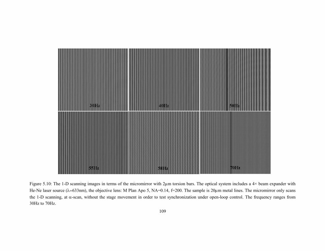
109
Figure 5.10: The 1-D scanning images in terms of the micromirror with 2m torsion bars. The optical system includes a 4× beam expander with
He-Ne laser source (633nm), the objective lens: M Plan Apo 5, NA=0.14, f=200. The sample is 20m metal lines. The micromirror only scans
the 1-D scanning, at -scan, without the stage movement in order to test synchronization under open-loop control. The frequency ranges from
30Hz to 70Hz.
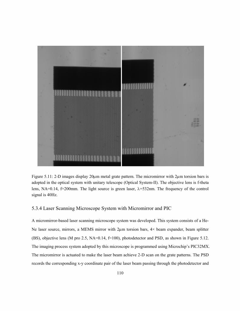
110
Figure 5.11: 2-D images display 20m metal grate pattern. The micromirror with 2m torsion bars is
adopted in the optical system with unitary telescope (Optical System-II). The objective lens is f-theta
lens, NA=0.14, f=200mm. The light source is green laser, =532nm. The frequency of the control
signal is 40Hz.
5.3.4 Laser Scanning Microscope System with Micromirror and PIC
A micromirror-based laser scanning microscope system was developed. This system consists of a He-
Ne laser source, mirrors, a MEMS mirror with 2m torsion bars, 4× beam expander, beam splitter
(BS), objective lens (M pro 2.5, NA=0.14, f=100), photodetector and PSD, as shown in Figure 5.12.
The imaging process system adopted by this microscope is programmed using Microchip‘s PIC32MX.
The micromirror is actuated to make the laser beam achieve 2-D scan on the grate patterns. The PSD
records the corresponding x-y coordinate pair of the laser beam passing through the photodetector and

111
instantaneously displays the light intensity on the LCD. This approach is referred to as the position-
based synchronization method for tracking outputs of the micromirror scan.
The control signal driving the micromirror is a triangle waveform with rounded corners. The
control signal is similar to that of the MACROscope. It helps to reduce overshoots of the micromirror
due to the discontinuities at the peaks of triangle waves. The amount of time it takes to finish one scan
is approximately 200seconds, which is the X-direction of -scan frequency at 5mHz and the Y-
direction scanning at 1Hz due to the slow ADC limitation by the PIC. But this is not the limiting
factor of the scanning rate. If a high quality ADC chip were adopted, the data acquisition rate could
be increased and the scanning rate might be higher. Figure 5.13 shows the output images on LCD.
The sample pattern is at least 50 micrometers in terms of this system. If different objective lens with
high numerical aperture were adopted, this system could achieve the sample images with higher
resolution.
Figure 5.12: The laser scanning microscope system with a MEMS micromirror with 2m torsion bars.

112
(a)
(b)
Figure 5.13: The grate pattern images from LSMS on PIC LCD. The frame size is 240×320pixels.

113
5.4 Conclusion
This chapter presents the micromirror with SW electrodes applied into the MACROscope for imaging.
In terms of two optical system configurations, Optical System-I provides higher resolution than
Optical System-II due to the beam expander enlarging the beam and increasing the effective
numerical aperture. Although the micromirror is actuated under the open-loop control, it could
provide acceptable dynamic response at optimized frequency so as to satisfy the synchronization
requirement for the system. Moreover, a novel laser scanning microscope system with the
micromirror is developed and obtains 2D images. The resolution power for the system is rated at
50m and the image acquisition time is too slow, however, it might be improved by changing
objective lens with high NA and using high quality ADC chip on the control circuit.
In this chapter, only the illumination path is shown in Confocal MACROscope system due to
simplify the testing process. In order to achieve a real confocal microscope, the system needs to have
the following features and changes:
addition of pin holes after the micromirror such that the reflective or emitted light can be
acquired by the sensor,
reposition of the light sensor-photon multiplier tube (PMT) for the weak signal detection,
optimization of micromirror scanning range, spacial resolution, and pixels.

114
Chapter 6
Conclusions and Future Research
6.1 Summary and Conclusions
The work presented in this thesis addresses two major challenges during developing the MEMS
mirror: i) the analytical modeling of SW electrodes and 3-end serpentine torsion bars and ii) the novel
fabrication process developed in terms of the design of a biaxial micromirror with SW electrodes.
Moreover, the development of Micromirror-based MACROscope and the prototype of a Micromirror-
based Laser Scanning Microscope provide a system platform for studying the micromirror
performance in optical applications.
The SW electrode actuator is a new electrostatic actuator that fills the gap between comb-drive and
parallel-plate actuators. There exist two major advantages: obtaining a large angular deflection under
a corresponding small drive voltage and possessing a simple fabrication process same as that of
parallel-plate actuators. The analytical modeling of SW electrodes and 3-end serpentine torsion bars
simulates the static and dynamic characteristics of the biaxial MEMS mirror with SW electrodes very
well at small scanning angles. This can be used as a very good reference during the design phases
before a commitment to a fabrication runs. Chapter 2 devotes to build the analytical modeling of SW
electrodes. In Chapter 3, this analytical modeling is improved in terms of practical design of the
MEMS mirror with SW electrodes. The developed analytical modeling is less consuming time than
commercial FEM/BEM simulations.

115
The fabrication process of the biaxial MEMS mirror with SW electrodes is based on SOI wafer,
hybrid bulk/surface micromachined technologies and a high-aspect-ratio shadow mask. In order to
obtain a large scanning angle, the gap between the micromirror plate and the bottom electrodes is
around 300m. The height of the SW electrodes is 250m. The material of serpentine torsion bars is
based on single crystal silicon. Built on a SOI wafer, the thickness of torsion bars is 12m accurately.
The fabrication process consists of three phases: mirror plate fabrication, SW electrode fabrication
and assembly of mirror plate and SW electrodes. The mirror plate fabrication includes front-side
fabrication and back-side fabrication on the SOI wafer. The expected thickness of the mirror plate can
be achieved. The SW electrode fabrication comprises bulk SW electrodes fabricated on a SOI wafer
and a high-aspect-ratio shadow mask. The shadow mask is built on a SCS wafer with the thickness of
250m or 285m, which patterns bottom electrodes, pads, and wires on the bulk SW electrodes.
Those shadow masks can be recycled and used repeatedly. A transparent alignment tool was
fabricated and used to assemble the mirror plate and the SW electrodes. The single micromirror
fabrication is founded in Chapter 3 and the micromirror array fabrication in Chapter 4. Although the
fabrication of micromirror arrays resembles that of the single micromirror, plenty of optimization on
mirror array structure design and fabrication parameters is required. Several types of the micromirror
with SW electrodes are obtained: single biaxial MEMS mirrors with 3m, 2m and 1.5m 3-end
serpentine torsion bars, single biaxial MEMS mirrors with 2-end serpentine torsion bars, and 2×2 and
4×4 micromirror arrays.
In Chapter 5 the performance of a biaxial MEMS mirror with SW electrodes in the MACROscope
was studied. The MACROscope system from BPI adopts a galvo-scanner and XYZ-stage to acquire
laser beam scanning and gain high resolution images with a large FOV. The biaxial MEMS mirror
replaces the galvo-scanner to simplify the design of the MACROscope. In terms of two optical
configurations tested in the MACROscope, optical requirements of the system based on a biaxial
MEMS mirror are studied. On the other hand, frequency optimization of the MEMS mirror is
achieved in terms of the MACROscope control requirements. Meanwhile, a Micromirror-based Laser
Scanning Microscope system is built and obtains 2-D images.

116
6.2 Future Works
This thesis presents the design, fabrication, and characterization of a 2-D SOI MEMS micromirror
with SW electrodes for Confocal MACROscope imaging. The single biaxial MEMS mirror with SW
electrodes, 2×2 and 4×4 micromirror arrays are obtained in terms of hybrid bulk/surface
micromachined technologies. The improvement of Confocal MACROscope integrated with a biaxial
micromirror and the prototype of Micromirror-based Laser Scanning Microscope are obtained. For
the future direction, they include several works:
i) Improvement on the analytical modeling of SW electrodes at large angular deflection: In this
range, the nonlinear property of 3-end serpentine torsion bars and fringe field effects on the
electrostatic field need to be understood. Meanwhile, when the MEMS mirror with SW electrodes
reaches a large angular deflection, either on -scan around ±10º (mechanical angle), an oscillation
phenomenon can be observed. This requires an explanation based on the improved modeling.
ii) Accomplishment on the confocal path of the MACROscope system: Although optical
requirements and optimized frequency for the MEMS mirror based on the illumination path of the
MACROscope has been obtained, there exists a distance to build a real confocal microscope. In order
to build a Micromirror-based Confocal MACROscope, the confocal path is required by adding an
optical fiber as a pinhole in the optical system. The relative adjustments and tests have to be
implemented.
iii) Develop an endoscopic probe with MEMS mirrors and implement the endoscope with OCT or
confocal microscope.
iv) Study control methods for driving micromirror arrays. Apply 2×2 and 4×4 micromirror arrays
into confocal microscope to increase effective optical aperture and obtain higher resolution images
.

117
Bibliography
[1] M. J. Madou, Fundamentals of Microfabrication, Boca Raton, Fla.: CRC Press c1997
[2] D. A. Horsley, W. O. Davis, K. J. Hogan, M. R. Hart, E. C. Ying, M. Chaparala, B. Behin, M.
J. Daneman, and M.-H. Kiang, ―Optical and mechanical performance of a novel magnetically
actuated MEMS-based optical switch,‖ J. Microelectromech. Syst., vol.14, no.2, pp.274-84,
2005
[3] I. W. Jung, Y. A. Peter, E. Carr, J. S. Wang, and O. Solgaard, ―Single-crystal-silicon
continuous membrane deformable mirror array for adaptive optics in space-based telescopes,‖
IEEE J. Sel. Topics Quantum Electron., vol. 13, vo. 2, pp.162-167, 2007
[4] S. J. Kim, Y. H. Cho, H. J. Nam and J. U. Bu, ―Piezoelectrically pushed rotational
micromirrors using detached PZT actuators for wide-angle optical switch applications,‖ J.
Micromech. Microeng., vol.18, pp.125022 (7pp), 2008
[5] A. D. Yalcinkaya, O. Ergeneman, H. Urey, ―Polymer magnetic scanners for bar code
applications,‖ Sens. Actuators A, Phys., vol.135, pp.236-43, 2007
[6] A. D. Yalcinkaya, H. Urey, D. Brown, T. Montague, and R. Sprague, ―Two-axis
electromagnetic microscanner for high resolution displays,‖ J. Microelectromech. Syst., vol.15,
no.4, pp.786-94, 2006
[7] H. Xie, Y. Pan, G. K. Fedder, ―Endoscopic optical coherence tomographic imaging with a
CMOS-MEMS micromirror,‖ Sens. Actuators A, Phys., vol.103), pp.237-241, 2003

118
[8] J.T.W.Yeow, V.X.D.Yang,etc, A. Chahwan, M.L. Gordon, B. Qi, I.A.Vitkin, B.C. Wilson, and
A.A. Goldenberg, ―Micromachined 2-D scanner 3-D optical coherence tomography,‖ Sens.
Actuators A, Phys., vol.117, no.2, pp.331-340, 2005
[9] J.H. Lee, Y. C. Ko, D. H. Kong, J. M. Kim, K. B. Lee, and D. Y. Jeon, ―Design and fabrication
of scanning mirror for laser display,‖ Sens. Actuators A, Phys., vol.96, pp.223-230, 2002
[10] H. Miyajima, N. Asaoka, T. Isokawa, M. Ogata, Y. Aoki, M. Imai, O. Fujimori, M. Katashiro,
and K. Matsumoto, ―A MEMS electromagnetic optical scanner for a commercial confocal laser
scanning microscope,‖ J. Microelectromech. Syst., vol.12, vo. 3, pp.243-51, 2003
[11] N. Maluf, K. Williams, An introduction to microelectromechanical systems engineering , 2nd
ed, Boston ; London : Artech House c2004
[12] J. C. Tsai and M. C.Wu, ―Gimbal-less MEMS two-axis optical scanner array with high fill-
factor,‖ J. Microelectromech. Syst.,, vol.14, vo.6, pp.1323-1328, 2005
[13] L. J. Hornbeck, ―Deformable-mirror spatial light modulators,‖ in Proc. SPIE Critical Reviews
Series 1150 Spatial Light Modulators and Applications III, pp.86-102. 1989
[14] L. J. Hornbeck, ―Current status of the digital micromirror device (DMD) for projection
television applications,‖ IEDM 93, IEEE 1993, pp.381-384, 1993
[15] H. Toshiyoshi, W. Piyawattanametha, C. T. Chan, and M. C. Wu, ―Linearization of
electrostatically actuated surface micromachined 2-D optical scanner, ‖ J. Microelectromech.
Syst. vol.10, no.2, pp.205-214, 2001
[16] K. Cao, W. Liu, and J. J. Talghader, ―Curvature compensation in micromirrors with high-
reflectivity optical coatings,‖ J. Microelectromech. Syst., vol.10, no.3, pp.409-417, 2001
[17] Y. H. Min and Y. K. Kim, ―Modeling, design, fabrication and measurement of a single layer
polysilicon micromirror with initial curvature compensation,‖ Sens. Actuators A, Phys., vol.78,
pp.8-17, 1999

119
[18] C. H. Tien, and C. H. Lee, ―Optical properties of surface micromachining with randomly
distributed etch holes,‖ Jpn. J. Appl. Phys., vol.45,no2A, pp.1015-1017, 2006
[19] J. Zou, M. Balberg, C. Byrne, C. Liu, and D. J. Brady, ―Optical properties of surface
micromachined mirrors with etch holes,‖ J. Microelectromech. Syst., vol.8, no.4, pp.506-513,
1999
[20] C. Pu, S. Park, P. B. Chu, S. S. Lee, M. Tsai, D. Peale, N. H. Bonadeo, and I. Brener,
―Electrostatic actuation of three-dimensional MEMS mirrors using sidewall electrodes,‖ IEEE
J. Sel. Topics Quantum Electron., vol.10, no.3, pp.472-77, 2004
[21] S. Kwon, V. Milanovic, and L. P. Lee, ―Vertical combdrive based 2-D gimbaled micromirrors
with large static rotation by backside island isolation,‖ IEEE J. Sel. Topics Quantum Electron.,
vol.10, no.3, 2004
[22] V. Milanovic, G. A. Matus, and D. T. McCormick, ―Gimbal-less monolithic silicon actuators
for tip-tilt-piston micromirror applications,‖ IEEE J. Sel. Topics Quantum Electron., vol. 10,
no. 3, pp.462-71, 2004
[23] T.D.Kudrle, C.C.Wang, M.G..Bancu, J.C.Hsiao,A.Pareek, M.Waelti, G.A.Kirkos, T.Shone,
C.D.Fung, C.H.Mastrangelo, ―Single-crystal silicon micromirror array with polysilicon
flexures‖, Sens. Actuators A, Phys., vol.119, no. , pp.559-566, 2005
[24] K. Murakami, ―A miniature confocal optical scanning microscope for endoscope,‖in Proc.
SPIE MOEMS Display and Imaging Systems III, vol.5721, Bellingham, WA, 2005
[25] K. Jia, S. Pal, H. Xie, ―An electrothermal tip-tilt-piston micromirror based on folded dual S-
shaped bimorphs,‖ J. Microelectromech. Syst., vol. 18, no.5, 2009
[26] J. Singh, J.H.S. Teo, Y. Yu, C.S. Premachandran, N. Chen, R. Kotlanka, M. Olivo and C.J.R.
Sheppard, ―A two axes scanning SOI MEMS micromirror for endoscopic bioimaging,‖ J.
Micromech. Microeng., vol.18, pp.025001(9pp), 2008

120
[27] A. Jain, A. Kopa, Y. Pan, G. K. Fedder, and H. Xie, ―A two-axis electrothermal micromirror
for endoscopic optical coherence tomography,‖ IEEE J. Sel. Topics Quantum Electron., vol.
10, no. 3, pp.636-642, 2004.
[28] K. E. Petersen, ―Silicon as a mechanical material,‖ in Proc. IEEE, vol.70, no.5, pp.420-
457,1982
[29] T. Tsutsumino, Y. Suzuki, N. Sakurai, N. Kasagi, and Y. Sakane, ―Nano-metal-ink-based
electrode embedded in parylene HARS with the aid of the capillary effect,‖ in Proc. IEEE 20th
Int. Conf. MEMS, Korea, pp.313-16, 2007
[30] C.H. Ji and Y.K. Kim, ―Electromagnetic micromirror array with single-crystal silicon mirror
plate and aluminum spring,‖ J. Lightwave Tech., vol.21, no.3, pp.584-90, 2003
[31] S. K. Lee, M. G. Kim, J. Y. An, M. H. Jun, S. Yang, and J. H. Lee, ―Polymeric (SU-8) optical
microscanner driven by electrostatic actuation,‖ in Proc. IEEE 22nd Int. Conf. MEMS, pp.955-
958, 2009
[32] C.S. Huang, Y.T. Cheng, J. Chung, W. Hsu, ―Investigation of Ni-based thermal bimaterial
structure for sensor and actuator application,‖ Sens. Actuators A, Phys., vol.149, pp.298-304,
2009
[33] L. Wu and H. Xie, ―124o rotation angle electrothermal micromirror with integrated platinum
heater,‖, IEEE J. Sel. Topics Quantum Electron., vol.13, no.2, 2007
[34] K. Jia, S. R. Samuelson and H. Xie, ―Single-wafer solution and optical phased array application
of micro-mirror arrays with high fill factor and large sub-apertures,‖ in Proc. IEEE Int. Conf.
23th MEMS, Hongkong, pp.180-183, 2010
[35] I. J. Cho and E. Yoon, ―A low-voltage three-axis electromagnetically actuated micromirror for
fine alignment among optical devices,‖ J. Micromech. Microeng., vol.19, pp.085007 (8pp),
2009

121
[36] S. H. Hung, H. T. Hsieh and G. D. J. Su, ―An electro-magnetic micromachined actuator
monolithically integrated with a vertical shutter for variable optical attenuation,‖ J. Micromech.
Microeng.,vol.18, pp.075003(8pp), 2008
[37] H. M. Jeong, Y. H. Park, Y. C. Cho, J. Hwang, S. M. Chang, S. J. Kang, H. K. Jeong, J. O.
Kim, J. H. Lee, ―Slow scanning electromagnetic scanner for laser display,‖ J. Micro/Nanolith.
MEMS MOEMS, vol.7, no.4, pp.043003-13pp, 2008
[38] H. Miyajima, ―Development of a MEMS electromagnetic optical scanner for a commercial
laser scanning,‖ J. Microlith., Microfab., Microsyst., vol.3, no.2, pp.348-57, 2004
[39] S. Schonhardt, J.G. Korvink, J. Mohr, U. Hollenbach and U. Wallrabe, ―Magnetic comb drive
actuator,‖ in Proc. IEEE Int. Conf. 23th MEMS, Hongkong, China, pp.479-80, 2010
[40] S. O. Isikman, O. Ergeneman, A. D. Yalcinkaya, and H. Urey, ―Modeling and characterization
of soft magnetic film actuated 2-D scanners,‖ IEEE J. Sel. Topics Quantum Electron., vol.12,
no.2, pp.283-89, 2007
[41] D. A. Horsley, W. O. Davis, K.J. Hogan, M.R. Hart, E. C. Ying, M. Chaparala, B. Behin, M. J.
Daneman, and M. H. Kiang, ―Optical and mechanical performance of a novel magnetically
actuated MEMS-based optical switch,‖ J. Microelectromech. Syst., vol.14, no.2, pp.274-84,
2005
[42] S. Brugger and O. Paul, ―Resonant magnetic microsensor with uT resolution,‖ in Proc. IEEE
Int. Conf. 21st MEMS, Tucson, AZ, USA, pp.944-947, 2008
[43] J. J. Bernstein, T. W. Lee, F. J. Rogomentich, M. G. Bancu, K. H. Kim, G. Maguluri, B. E.
Bouma, J. F. DeBoer, ―Scanning OCT endoscope with 2-axis magnetic micromirror,‖ in Proc.
SPIE Endoscopic Microscopy II, vol. 6432, pp.64320L, 2007
[44] K. H. Kim, B. H. Park, G. N. Maguluri, T. W. Lee, F. J. Rogomentich, M. G. Bancu, B. E.
Bouma, J. F. de Boer, and J. J. Bernstein, ―Two-axis magnetically-driven MEMS scanning

122
catheter for endoscopic high-speed optical coherence tomography,‖ Opt. Exp., vol.15, no.26,
pp.18130, 2007
[45] J. Bernstein, W.P. Taylor, J. Brazzle, G. Kirkos, J. Odhner, A. Pareek, M. Zai, ―Two axis-of-
rotation mirror array using electromagnetic MEMS,‖ IEEE, pp275-8, 2003
[46] M. Jamet, et al., ―High-curie-temperature ferromagnetism in self-organized Ge1-xMnx
nanocolumns‖, Nature materials, vol.5, pp.653-659, 2006
[47] T. Kawabata, M. Ikeda, H. Goto, M. Matsumoto, and Y. Tsuneji, ―The 2-Dimentional micro
scanner integrated with PZT thin film actuator,‖ in Proc. IEEE 1997 Int. Conf. on Solid-State
Sensors and Actuators, pp.339-342. 1997
[48] J. M. Zara, and S. W. Smith, ―A micromachined high frequency ultrasound scanner using
photolithographic fabrication,‖ IEEE Trans. Ultrason. Ferroelectr. Freq. Control., vol.49,
no.7, 2002
[49] K. H. Koh, T. Kobayashi, F. L. Hsiao and C. Lee, ―A 2-D MEMS scanning mirror using
piezoelectric PZT beam actuators,‖ Procedia Chemistry, vol.1, pp.1303-1306, 2009
[50] S. J. Kim, Y. H. Cho, H. J. Nam and J. U. Bu, ―Piezoelectrically pushed rotational
micromirrors using detached PZT actuators for wide-angle optical switch applications,‖ J.
Micromech. Microeng., vol.18, pp.125022 (7pp), 2008
[51] C. Lee, F. L. Hsiao, T. Kobayashi, K. H. Koh, P. V. Ramana, W. Xiang, B. Yang, C. W. Tan,
and D. Pinjala, ―A 1-V operated MEMS variable optical attenuator using piezoelectric PZT
thin-film actuators,‖ IEEE J. Sel. Topics Quantum Electron., vol.15, no. 5, 2009
[52] P. Muralt, ―PZT thin films for microsensors and actuators: where do we stand?‖, IEEE Trans.
Ultrason. Ferroelectr. Freq. Control., vol.47, no.4, pp.903-915, 2000
[53] H. Zeng, A. D. Feinerman, Z. Wan, and P. R. Patel, ―Piston-motion micromirror based on
electrowetting of liquid metals,‖ J. Microelectromech. Syst., vol.14, no.2, pp.285-94, 2005

123
[54] J. Lee, H. Moon, J. Fowler, T. Schoellhammer, C. J. Kim, ―Electrowetting and electrowetting-
on-dielectric for microscale liquid handling,‖ Sens. Actuators A, Phys., vol.95, pp.259-268,
2002
[55] I. J. Cho and E. Yoon, ―Design and fabrication of a single membrane push-pull SPDT RF
MEMS switch operated by electromagnetic actuation and electrostatic hold,‖ J. Micromech.
Microeng., vol.20, pp.035028(7pp), 2010
[56] Y. Eun, H. Na, B. Jeong, J. Lee, ―Bidirectional electrothermal electromagnetic torsional
microactuators for large angular motion at dc mode and high frequency resonance mode
operation,‖ J. Micromech. Microeng., vol.19, pp.(8pp), 2009
[57] Ph. Robert, D. Saias, C. Billard, S. Boret, N. Sillon, C. Maeger-Pachurka, P. L. Charvet, G.
Bouche, P. Ancey and P. Berruyer, ―Integrated RF-MEMS switch based on a combincation of
thermal and electrostatic actuation,‖ in Proc. IEEE 12th Int. Conf. Solid-State Sens., Actuators,
Microsyst. Transducers, Boston, MA, pp.1714-17, 2003
[58] A. Alwan and N. R. Aluru, ―Analysis of hybrid electrothermomechanical microactuators with
integrated electrothermal and electrostatic actuation,‖ J. Microelectromech. Syst., vol.18, no.5,
pp.1126-36, 2009
[59] D. Hah, P. R. Patterson, H. D. Nguyen, H. Toshiyoshi, and M. C. Wu, ― Theory and
experiments of angular vertical comb-drive actuators for scanning micromirrors,‖, IEEE J. Sel.
Topics Quantum Electron., vol.10, no.3, pp.505-513, 2004
[60] D. Hah, S. T.Y. Huang, J. C. Tsai, H. Toshiyoshi, and M. C. Wu, ―Low-Voltage, large-scan
angle MEMS analog micromirror arrays with hidden vertical comb-drive actuators,‖ J.
Microelectromech. Syst., vol.13, no.2, pp.279-289, 2004

124
[61] S. Kwon, V. Milanovic, and L. P. Lee, ―Vertical combdrive based 2-D gimbaled micromirrors
with large static rotation by Backside island isolation‖, IEEE J. Sel. Topics Quantum Electron.,
vol.10, no.3, pp.498-504, 2004
[62] U. Krishnamoorthy, D. Lee, and O. Solgaard, ―Self-aligned vertical electrostatic combdrives
for micromirror actuation,‖ J. Microelectromechn. Syst., vol.12, no.4, pp.458-64, 2003
[63] H. Xie, Y. Pan, and G. K. Fedder, ―A CMOS-MEMS mirror with curled-hinge combdrives,‖ J.
Microelectromech. Syst. vol.12, no.4, pp.450-457, 2003
[64] C. Siu, H. Zeng, and M. Chiao, ―Magnetically actuated MEMS microlens scanner for in vivo
medical imaging‖, Opt. Exp., Vol.15, No. 18, 11154-11166, Sept. 2007
[65] Z. Yaqoob, J. Wu, E. J. McDowell, X. Heng, C. Yang, ―Methods and application areas of
endoscopic optical coherence tomography‖, J. Biomed. Opt., vol.11, no.6, pp.1-19, 2006
[66] B. E. Bouma, G. J. Tearney, Handbook of Optical Coherence Tomography , NewYork: Marcel
Dekker, 2002
[67] J.B. Pawley, Handbook of Biological Confocal Microscopy, 3rd ed., Berlin: Springer.2006
[68] J. M. Zara, S. Yazdanfar, K. D. Rao, J. A. Izatt, and S. W. Smith, ―Electrostatic micromachine
scanning mirror for optical coherence tomography‖, Opt. Lett., vol.28, no.8, 2003
[69] T Mitsui, Y Takahashi and Y Watanabe, ―A 2-axis optical scanner driven nonresonantly by
electromagnetic force for OCT imaging‖, J. Micromech. Microeng., vol.16, pp.2482–2487,
2006
[70] T. Xie, H. Xie, G.K. Fedder and Y. Pan , ―Endoscopic optical coherence tomography with new
MEMS mirror‖, Electron. Lett., vol.39, no.21, 2003
[71] L. Wu and H. Xie, ―A Dual Reflective Electrothermal MEMS Micromirror for Full
Circumferential Scanning Endoscopic Imaging‖, in Proc. SPIE, vol. 6885, 688508-1~8, 2008

125
[72] L. Fu, A. Jain, C. Cranfield, H. Xie, and M. Gua, ―Three-dimensional nonlinear optical
endoscopy‖, J. Biomed. Opt.,vol.12,no.4, 2007
[73] J. Woonggyu, T. McC. Daniel, Z. Jun, W. Lei, C.T. Norman, Z.P. Chen, ―Three-dimensional
endoscopic optical coherence tomography by use of a two-axis microelectromechanical
scanning mirror‖, Appl. Phys. Lett., vol.88, pp.1-3, 2006
[74] J. Woonggyu, T.M. Daniel, Y.C. Ahn, A. Sepehr, M. Brenner, B. Wong, N.C. Tien, and Z.
Chen, ― In vivo three-dimensional spectral domain endoscopic optical coherence tomography
using a microelectromechanical system mirror‖, Opt. Lett., vol.32, no.22, pp.3239-3241, 2007
[75] J. M. Zara, C. A. Lingley-Papadopoulos, ―Endoscopic OCT approaches toward cancer
diagnosis‖, IEEE Journal of selected topics in quantum electronics, vol.14, no.1, pp.70-81,
2008
[76] D. Huang, E. A. Swanson, C. P. Lin, J. S. Schuman, W. G. Stinson, W. Chang, M. R. Hee, T.
Flotte, K. Gregory, C. A. Puliafito, J. G. Fujimoto, ―Optical coherence tomography,‖ Science,
vol.254, pp.1178-1181, 1991
[77] A. F. Fercher, W. Drexler, C. K. Hitzenberger and T. Lasser, ―Optical coherenc tomography-
principles and applications‖, Rep. Prog. Phys., vol.66, pp.239-303, 2003
[78] M. E. Brezinski, Optical coherence tomography: Principles and Applications, Boston:
Academic Press, c2006
[79] A. F. Fercher, ―Optical coherence tomography,‖ J. Biomed. Opt., vol. 1, no. 3, pp. 157–
173,1996
[80] V Prasad, D Semwogerere and Eric R Weeks, ―Confocal microscopy of colloids‖, J. Phys.:
Condens. Matter 19, pp.1-25, 2007
[81] Y. H. Bai, J. T. W.Yeow, B. C. Wilson, ―A characteristic study of micromirror with sidewall
Electrodes,‖ Int. J. Optomechatronics, vol.1, no.3, pp.231-258, 2007

126
[82] Y. H. Bai, J. T.W. Yeow, and B. C. Wilson, ―Design, fabrication, and characteristics of a
MEMS micromirror with sidewall electrodes,‖ J. Microelectromech. Syst., vol.19, no.3,
pp.619-631, 2010
[83] Y. H. Bai, J. T.W. Yeow, P. Constantinou, S. Damaskinos, and B. C.Wilson, ―A 2-D
micromachined SOI MEMS mirror with sidewall electrodes for biomedical imaging,‖
IEEE/ASME Trans. Mechatronics, vol.15, no.4, pp.501-510, 2010
[84] W. M. Duncan, T. Bartlett, B. Lee, D. Powell, P. Rancuret, and B. Sawyers, ―Dynamic optical
filtering in DWDM systems using the DMD,‖ Solid-state Electron., vol.46, pp.1583-1585,
2002.
[85] F. Khechana, H. van Lintel, J. L. Massieu, S. Ackley, and P. Renaud, ―Thermally actuated
micro scanner for barcode reader applications,‖ in Proc. IEEE/LEOS Int. Conf. on Optical
MEMS and Their Applications, pp.57-58, 2005.
[86] M. E. Motamedi, MOEMS: micro-opto-electro-mechanical systems, Washington: SPIE Press.
2005.
[87] J. Singh, T. Gan, A. Agarwal, Mohanraj, and S. Liw, ―3D free space thermally actuated
micromirror device,‖ Sens. Actuators A, Phys., vol.123, no.4, pp.468-475, 2005
[88] Y. Yee, H. J. Nam, S. H. Lee, J. U. Bu, Y. S. Jeon, and S. M. Cho, ―PZT actuated micromirror
for nano-tracking of laser beam for high-density optical data storage,‖ in Proc. IEEE 13th
Annual Int. Conf. on MEMS, pp.435-440, 2000
[89] X. M. Zhang, F. S. Chau, C. Quan, Y. L. Lam, and A. Q. Liu, ―A study of the static
characteristics of a torsional micromirror,‖ Sens. Actuators A, Phys., vol.90, pp.73-81, 2001
[90] J. P. Zhao, H. L. Chen, J. M. Huang, and A. Q. Liu, ―A study of dynamic characteristics and
simulation of MEMS torsional micromirrors,‖ Sens. Actuators A, Phys., vol.120, pp.199-210,
2005

127
[91] Z. Hao, B. Wingfield, M. Whiteley, J. Brooks, and J. A. Hammer, ―A design methodology for a
bulk-micromachined two-dimensional electrostatic torsion micromirror,‖ J. Microelectromech.
Syst., vol.12, no.5, pp.692-701, 2003
[92] Y. Yao, X. Zhang, G. Wang, and L. Huang, ―Efficient modeling of a biaxial micromirror with
decoupled mechanism,‖ Sens. Actuators A, Phys., vol.120, pp.7-16, 2005
[93] G. Zhou, F. E. H. Tay, and F. S. Chau, ―Macro-modelling of a double-gimballed electrostatic
torsional micromirror,‖ J. Micromech. Microeng., vol.13, pp.532-547, 2003
[94] H. Camon, and F. Larnaudie, ―Fabrication, simulation and experiment of rotating electrostatic
silicon mirror with large angular deflection,‖ in Proc. IEEE 13th Annual Int. Conf. on MEMS,
pp.645-650, 2000
[95] W. Cichalewski, A. Napieralski, H. Camon, and B. Estibals, ―Analytical modeling and
simulations of a MEMS micromirror – MATLAB implementation,‖ in Proc. IEEE 7th Int.
Conf. CADSM, pp.360-365, 2003
[96] D. L. Dickensheets, and G. S. Kino, ―Silicon-micromachined scanning confocal optical
microscope,‖ J. Microelectromech. Syst., vol.7, no.4, pp.38-47, 1998
[97] H. Toshiyoshi, and H. Fujita, ―Electrostatic micro torsion mirrors for an aptical switch matrix,‖
J. Microelectromech. Syst. vol.5, no.4, pp.231-237, 1996
[98] G. Zhu, M. Packirisamy, M. Hosseini, and Y. A. Peter, ―Modelling and control of an
electrostatically actuated torsional micromirror,‖ J. Micromech. Microeng., vol.16, pp.2044-
2052, 2006
[99] M. A. Hopcroft, W. D. Nix, and T. W. Kenny, ―What is the Young‘s Modulus of silicon?‖ J.
Microelectromech. Syst., vol.19, no.2, pp.229-238, 2010
[100] S. P. Timoshenko, and J. N. Goodier, Theory of Elasticity, 3rd ed. New York: McGraw-Hill.
1970.

128
[101] J. Chen, W. Weingartner, A. Azarov, and R. C. Giles, ―Tilt-angle stabilization of
electrostatically actuated micromechanical mirrors beyond the pull-in point,‖ J.
Microelectromech. Syst., vol.13, no.6, pp.988-997, 2004
[102] O. Degani, E. Socher, A. Lipson, T. Leitner, D. J. Setter, S. Kaldor, and Y. Nemirovsky, ―Pull-
in study of an electrostatic torsion microactuator,‖ J. Microelectromech. Syst., vol.7, no.4,
pp.373-379, 1998
[103] Y. Nemirovsky, and O. Degani, ―A methodology and model for the pull-in parameters of
electrostatic actuators,‖ J. Microelectromech. Syst., vol.10, no.4, pp.601-615, 2001
[104] Z. Xiao, W. Peng, X. T. Wu, and K. R. Farmer, ―Pull-in study for round double-gimbaled
electrostatic torsion actuators,‖ J. Micromech. Microeng., vol.12, pp.77-81, 2002
[105] ANSYS Release 8.0 Document.
[106] D. J. Inman, Engineering Vibration, 2nd ed. New Jersey:Prentice Hall. 2001
[107] F. Pan, J. Kubby, E. Peeters, A. T. Tran, and S. Mukherjee, ―Squeeze film damping effect on
the dynamics response of a MEMS torsion mirror,‖ J. Micromech. Microeng., vol.8, pp.200-
208, 1998
[108] T.J. Brosniham, S.A. Brown, A. Brogan, C.S. Gormley, D.J. Collins, S.J. Sherman, M. Lemkin,
N.A. Polce, M.S. Davis, ―Optical IMEMS-A fabrication process for MEMS optical switches
with integrated on-chip electronics,‖ in Proc. Transducers’03, 12th Int. Conf. Solid State Sens.
Actuators, and Micro-Systems, Boston, MA, 2003, pp.1638-1642
[109] Y. Yao, X. Zhang, G. Wang, and L. Huang, ―Efficient modeling of a biaxial micromirror with
decoupled mechanism,‖ Sens. Actuators A, Phys., vol.120, pp.7-16, 2005
[110] G. K. Fedder, Simulation of microelectromechanical systems, Ph.D. dissertation, Eng.-Elect.
Eng. Comp. Sci., California Univ., Berkeley, US, 1994

129
[111] G. Barillaro, A. Molfese, A. Nannini and F. Pieri, ―Analysis, simulation and relative
performances of two kinds of serpentine springs,‖ J. Micromech. Microeng., vol.15, no.4,
pp.736-746, 2005
[112] S.P. Timoshenko, and J. M. Gere, Mechanics of materials, New York: D. Van Nostrand
Company, 1972, pp. 8-11, 348-453
[113] http://www.on-trak.com
[114] J. H. Park, G. K. Garipov, J. A. Jeon, B. A. Khrenov, J. E. Kim, M. Kim, Y. K. Kim, C. H. Lee,
J. Lee, G. W. Na, S. Nam, I. H. Park, and Y. S. Park, ―Öbscura telescope with a MEMS
micromirror array for space observation of transient luminous phenomena or fast-moving
objects,‖ Opt. Exp., vol. 16, no. 25, pp.20249-20257, 2008
[115] M. Kim, J. H. Park, J. A. Jeon, B. W. Yoo, I. H. Park and Y. K. Kim, ―High fill-factor
micromirror array using a self-aligned vertical comb drive actuator with two rotational axes,‖ J.
Micromech. Microeng., vol.19, pp.035014(9pp), 2009
[116] U. Krishnamoorthy, K. Li, K. Yu, D. Lee, J.P. Heritage, O. Solgaard, ―Dual-mode
micromirrors for optical phased array applications,‖ Sens. Actuators A, Phys., vol.97-98, pp.21-
26, 2002
[117] K. Jia, S. R. Samuelson and H. Xie, ―Single-wafer solution and optical phased array application
of micro-mirror arrays with high fill factor and large sub-apertures,‖ in Proc. IEEE 23th Int.
Conf. MEMS, Hongkong, China, pp.180-83, 2010
[118] P. Lane, A. Dlugan, and C. MacAulay, ―DMD-enabled confocal microendoscopy,‖ in Proc.
SPIE, vol.4251, pp.192-198, 2001
[119] P. F. Mcmanamon, T. A. Dorschner, D. L. Corkum, L. J. Friedman, D. S. Hobbs, M. Holz, S.
Liberman, H. Q. Nguyen, D. P. Resler, R. C. Sharp, and E. A. Watson, ―Optical phased array
technology,‖ in Proc. IEEE, vol.84, no.2, 1996

130
[120] W. Jung, U. Krishnamoorthy, and O. Solgaard, ―High fill-factor two-axis gimbaled tip-tilt-
piston micromirror array actuated by self-algined vertical electrostatic combdrives,‖ J.
Microelectromech. Syst., vol. 15, no. 3, pp.563-71, 2006
[121] G. J. Burger, E. J. T. Smulders, J. W. Berenschot, T. S. J. Lammerink, J. H. J. Fluitman, S. Imai,
―High-resolution shadow-mask patternning in deep holes and its application to an electrical
wafer feed-through,‖ Sens. Actuators A, Phys., vol.54, pp.669-73, 1996
[122] M. Minsky, ―Microscopy Apparatus,‖ U.S. Patent, 301467, 1961
[123] J. T. Soini, M. Schrader, P. E. Hanninen, and S. W. Hell, ―Image formation and data
acquisition in a stage scanning 4Pi confocal fluorescence microscope,‖ Appl. Opt., vol.36,
no.34, pp.8929-8934, 1997
[124] W. Denk, J. H. Strickler, and W. W. Webb, ―Two-photon laser scanning fluorescene
microscopy,‖ Science, vol.248, no. 4951, pp.73-76, 1990
[125] C. L. Hoy, N. J. Durr, P. Chen, W. Piyawattanametha, H. Ra, O. Solgaard, and A. B. Yakar,
―Miniaturized probe for femtosecond laser microsurgery and two-photon imaging,‖ Opt. Exp.,
vol.16, no.13, pp.9996-10005, 2008
[126] W. Piyawattanametha, R. P. J. Barretto, T. H. Ko, B. A. Flusberg, and E. D. Cocker, ―Fast-
scanning two-photon fluorescence imaging based on a microelectromechanical systems two-
dimensional scanning mirror,‖ Opt. Lett., vol.31, no.13, pp.2018-20, 2006
[127] H. Miyajima, M. Nishio, Y. Kamiya, M. Ogata, Y. Sakai, and H. Inoue, ―Development of two
dimensional scanner-on-scanner for confocal laser scanning microscope ‗LEXT‘ Series,‖ in
Proc. IEEE/LEOS Int. Conf. on Optical MEMS and Their Applications, pp.23-24, 2005
[128] http://www.olympusfluoview.com/theory/index.html

131
[129] H. Ra, W. Piyawattanametha, M. J. Mandella, P. L. Hsiung, J. Hardy, T. D. Wang, C. H.
Contag, G. S. Kino, and O. Solgaard, ―Three-dimensional in vivo imaging by a handheld dual-
axes confocal microscope,‖ Opt. Exp., vol.16, no.10, pp.7224-32, 2008
[130] H. J. Shin, M. C. Pierce, D. Lee, H. Ra, O. Solgaard, and R. Richards-Kortum, ―Fiber optic
confocal microscope using a MEMS scanner and miniature objective lens,‖ Opt. Exp., vol.15,
no.15, pp.9113-9122, 2007
[131] K. Kumar, K. Hoshino, and X. Zhang, ―Handheld subcellular-resolution single-fiber confocal
microscope using high-reflectivity two-axis vertical combdrive silicon microscanner,‖ Biomed
Microdevices, vol. ,pp.653-60, 2008
[132] K. Kumar, R. Avritscher, Y. Wang, N. Lane, D. C. Madoff, T. Yu, J. W. Uhr, X. Zhang,
―Handheld histology-equivalent sectioning laser-scanning confocal optical microscope for
interventional imaging,‖ Biomed Microdevices, vol.12, pp.223-33, 2010
[133] H. Gruger, J. Knobbe, T. Egloff, M. Althaus, M. Scholles, H. Schenk, ―Scanning photon
microscope based on a MEMS 2D scanner mirror,‖ in Proc. SPIE, vol.7208, 72080D, 2009
[134] J. Helfmann, R. Schutz, I. Gersonde, G. Illing, ―MEMS-based confocal laser scanning
microscope for in vivo imaging,‖ in Proc. SPIE, vol.7367, 73671P, 2009
[135] C. L. Arrasmith, C. A. Patil, D. L. Dickensheets, A. Mahadevan-Jansen, ―A MEMS based
handheld confocal microscope with Raman spectroscopy for in-vivo skin cancer diagnosis,‖ in
Proc. SPIE, vol.7169, 71690, 2009
[136] A. Jain and H. Xie, ―Endoscopic microprobe with a LVD microlens scanner for confocal
imaging,‖ IEEE 2006, pp.168-9, 2006
[137] K. C. Maitland, H. J. Shin, H. Ra, D. Lee, O. Solgaard, and R. Richards-Kortum, ―Single fiber
confocal microscope with a two-axis gimbaled MEMS scanner for cellular imaging,‖ Opt. Exp.,
vol.14, no.9, pp.8604-8612, 2006

132
[138] P. Constantinou, T. Nicklee, D. W. Hedley, S. Damaskinos, and B. C. Wilson, ―A high-
resolution MACROscope with differential phase contrast, transmitted light, confocal
fluorescence and hyperspectral capabilities for large-area tissue imaging,‖ IEEE J. Sel. Topics
Quantum Electron., vol.11, no.4, pp.766-777, 2005
[139] G. F. Marshall, Optical Scanning, New York: Marcel Dekker Inc. c1991

133
Appendices

134
Appendix A
Integral factor of electrode e11 :
dxdyyxg
yG
Se
ef
2
11
11sinsincos
1sin
(A.1)
dxdyyxg
xG
Se
ef
2
11
11sinsincos
1sin
(A.2)
dxdyyxg
G
Se
fZe
2
11
11sinsincos
1sincos
(A.3)
Integral factor of electrode e12 :
12
2
12cossinsin2/
1)sin(
Se
ef dxdyyxLe
yG
(A.4)
dxdyyxLe
xG
Se
ef
2
12
12cossinsin2/
1)sin(
(A.5)
dxdyyxLe
G
Se
fZe
2
12
12cossinsin2/
1)sin()2/cos(
(A.6)
Integral factor of electrode e13 :
dxdyxLe
yG
Se
ef
2
13
13cos2/
1)sin(
(A.7)
dxdyxLe
xG
Se
ef
2
13
13cos2/
1)sin(
(A.8)
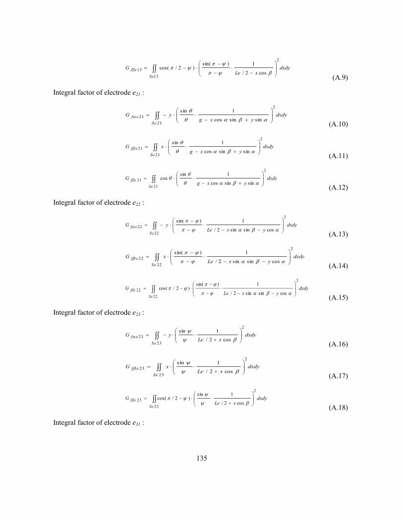
135
dxdyxLe
G
Se
fZe
2
13
13cos2/
1)sin()2/cos(
(A.9)
Integral factor of electrode e21 :
dxdyyxg
yG
Se
ef
2
21
21sinsincos
1sin
(A.10)
dxdyyxg
xG
Se
ef
2
21
21sinsincos
1sin
(A.11)
dxdyyxg
G
Se
fZe
2
21
21sinsincos
1sincos
(A.12)
Integral factor of electrode e22 :
22
2
22cossinsin2/
1)sin(
Se
ef dxdyyxLe
yG
(A.13)
dxdyyxLe
xG
Se
ef
2
22
22cossinsin2/
1)sin(
(A.14)
dxdyyxLe
G
Se
fZe
2
22
22cossinsin2/
1)sin()2/cos(
(A.15)
Integral factor of electrode e23 :
23
2
23cos2/
1sin
Se
ef dxdyxLe
yG
(A.16)
dxdyxLe
xG
Se
ef
23
2
23cos2/
1sin
(A.17)
dxdyxLe
G
Se
fZe
2
23
23cos2/
1sin)2/cos(
(A.18)
Integral factor of electrode e31 :

136
dxdyyxg
yG
Se
ef
2
31
31sinsincos
1sin
(A.19)
dxdyyxg
xG
Se
ef
2
31
31sinsincos
1sin
(A.20)
dxdyyxg
G
Se
fZe
2
31
31sinsincos
1sincos
(A.21)
Integral factor of electrode e32 :
dxdyyxLe
yG
Se
ef
2
32
32cossinsin2/
1sin
(A.22)
dxdyyxLe
xG
Se
ef
2
32
32cossinsin2/
1sin
(A.23)
dxdyyxLe
G
Se
fZe
32
2
32cossinsin2/
1sin)2/cos(
(A.24)
Integral factor of electrode e33 :
dxdyxLe
yG
Se
ef
2
33
33cos2/
1sin
(A.25)
33
2
33cos2/
1sin
Se
ef dxdyxLe
xG
(A.26)
dxdyxLe
G
Se
fZe
2
33
33cos2/
1sin)2/cos(
(A.27)
Integral factor of electrode e41 :
dxdyyxg
yG
Se
ef
41
2
41sinsincos
1sin
(A.28)
dxdyyxg
xG
Se
ef
2
41
41sinsincos
1sin
(A.29)

137
dxdyyxg
G
Se
fZe
2
41
41sinsincos
1sincos
(A.30)
Integral factor of electrode e42 :
dxdyyxLe
yG
Se
ef
2
42
42cossinsin2/
1sin
(A.31)
dxdyyxLe
xG
Se
ef
2
42
42cossinsin2/
1sin
(A.32)
dxdyyxLe
G
Se
fZe
42
2
42cossinsin2/
1sin)2/cos(
(A.33)
Integral factor of electrode e43 :
dxdyxLe
yG
Se
ef
2
43
43cos2/
1)sin(
(A.34)
dxdyxLe
xG
Se
ef
2
43
43cos2/
1)sin(
(A.35)
dxdyxLe
G
Se
fZe
2
43
43cos2/
1)sin()2/cos(
(A.36)