Design and Analysis of Integrated RF Front-End …€¦ · · 2017-10-24Design and Analysis of...
5
Design and Analysis of Integrated RF Front-end Transceiver System Using Printed Circuit Technology for 5 GHz Wireless Communication Applications Yasser M. Madany Senior, Member IEEE, Comm. and Electro. Dep., Alexandria University, Alexandria, Egypt. [email protected] Nour Eldin H. Ismail Communications and Electronics Department, Alexandria University, Alexandria, Egypt. Hayman A. Hassan Communications and Electronics Department, Alexandria University, Alexandria, Egypt. [email protected] Abstract—The wireless market is developing very fast today with a steadily increasing number of users all around the world. An increasing number of users and the constant need for higher and higher data rates have led to an increasing number of emerging wireless communication standards. As a result there is a huge demand for flexible and low-cost radio architectures for portable applications. Modern radio trans- ceivers have to support several different standards. Moving towards multi-standard radio, a high level of integration becomes a necessity and only can be accomplished by new improved radio architectures and full utilization of technology scaling. A radio frequency (RF) front-end system has been designed, integrated and fabricated using printed circuit board (PCB). The system consists of single-pole double-throw (SPDT) transmitter/receiver (T/R) switch with PIN diode, a low noise amplifier (LNA), a power amplifier (PA) and other microwave components. The components and sub-circuits based upon the transmission line theory have been utilized for the system design. All the sub-circuits and the entire system have been evaluated using a commercial software. The full design has been fabricated and measured using network analyzer. It is shown that RF front-end system can be integrated in a PCB utilizing a conventional PCB process. This system integration technique provides not only low cost but also high performance because of the elimination of parasitic associated with lumped components in a conventional design. Keywords- RF front-end; SPDT; LNA; PA; integrated transceiver system; wireless communication applications. I. INTRODUCTION Wireless communication is today a very large and important market affecting our lives in many ways. The number of wireless standards is increasing for every year and higher data rates are requested by even more users than before. To make this possible a numerous number of different standards and technologies are used. A few examples are GSM, WCDMA, Bluetooth, and WLAN (802.11a, b, g . . ) [1]. The FCC’s allocation of 300 MHz of bandwidth in the 5 GHz frequency band (5.15–5.35/5.725– 5.825 GHz) for the unlicensed national information infrastructure (UNII), high data rate (up to 50 Mb/s) wireless local area networks (WLAN) have become increasingly popular and important for mobile computing devices such as notebook computers. The European counterpart is the HIPERLAN (High Performance Radio LAN) system, which also operates in the 5-GHz band (5.15–5.35/5.47–5.725 GHz). With the increased number of wireless standards used today it is no longer reasonable that customers should have one handset for each standard. From a customer’s perspective one handset capable of switching between all standards is the optimal solution. The simplest, and most straight forward, solution would of course be to include one chip-set for each standard into for example a mobile phone or a laptop. This would however also lead to a highly increased cost and a very bulky terminal with short standby time due to high power consumption. The smallest, cheapest, and most elegant solution would be to use a RF front-end capable of covering all possible standards, i.e., a software- defined radio. In this paper, RF front-end system has been introduced. The proposed structure has been designed using duroid substrate with ( r = 6.15, tan = 0.0019) and thickness of 0.635 mm. The characteristics of the proposed structure are obtained and analyzed using HFSS simulator [2] to demonstrate the performance. The compact integrated RF front-end system around 5 GHz, as a main frequency, has been fabricated and measured. II. RF FRONT-END SYSTEM DESIGN STRUCTURE A lot of effort has been made to seek an alternative or modified architecture to the conventional one such that the requirements of the image-rejection and IF filters can be relaxed. The ultimate goal is to completely eliminate these off-chip filters. Several receiver architectures have been conceived to implement the idea. The low-IF and direct- conversion (or zero IF) are two of the most well-known. Direct-conversion is believed to be the most simple and straightforward way to build a radio receiver [3]-[8]. By converting the RF signal directly to the base band, the image frequency no longer exists. A. SPDT-T/R Switch The proposed identical SPDT-T/R switch with PIN diode structure is shown in Fig. 1. In a typical transceiver system, primary aims are to direct high power RF signal from TX to ANT while preventing leakage of that large signal into more sensitive front-end of RX, as shown in Fig. 2. From Fig. 2, it was found that, in transmit mode (RF signals go through TX to ANT), the PIN diodes are turned 'OFF'. Then, TX coupled-resonator becomes all-pass response while in the receive arm, the PIN diodes are turned 'ON'. Then, the RX coupled-resonator becomes band-stop response. Hence, the additional isolation can be obtained and also the receive arm becomes absorptive port. The same operation can be obtained in the receive mode (RF signals go through ANT to 2014 First International Conference on Systems Informatics, Modelling and Simulation 978-0-7695-5198-2/14 $31.00 © 2014 IEEE DOI 10.1109/SIMS.2014.43 190 2014 First International Conference on Systems Informatics, Modelling and Simulation 978-0-7695-5198-2/14 $31.00 © 2014 IEEE DOI 10.1109/SIMS.2014.43 190 2014 First International Conference on Systems Informatics, Modelling and Simulation 978-0-7695-5198-2/14 $31.00 © 2014 IEEE DOI 10.1109/SIMS.2014.43 190
Transcript of Design and Analysis of Integrated RF Front-End …€¦ · · 2017-10-24Design and Analysis of...
Design and Analysis of Integrated RF Front-end Transceiver System Using Printed Circuit Technology for 5 GHz Wireless Communication Applications
Yasser M. Madany Senior, Member IEEE, Comm. and
Electro. Dep., Alexandria University, Alexandria, Egypt. [email protected]
Nour Eldin H. Ismail Communications and Electronics
Department, Alexandria University, Alexandria, Egypt.
Hayman A. Hassan Communications and Electronics
Department, Alexandria University, Alexandria, Egypt.
Abstract—The wireless market is developing very fast today with a steadily increasing number of users all around the world. An increasing number of users and the constant need for higher and higher data rates have led to an increasing number of emerging wireless communication standards. As a result there is a huge demand for flexible and low-cost radio architectures for portable applications. Modern radio trans-ceivers have to support several different standards. Moving towards multi-standard radio, a high level of integration becomes a necessity and only can be accomplished by new improved radio architectures and full utilization of technology scaling. A radio frequency (RF) front-end system has been designed, integrated and fabricated using printed circuit board (PCB). The system consists of single-pole double-throw (SPDT) transmitter/receiver (T/R) switch with PIN diode, a low noise amplifier (LNA), a power amplifier (PA) and other microwave components. The components and sub-circuits based upon the transmission line theory have been utilized for the system design. All the sub-circuits and the entire system have been evaluated using a commercial software. The full design has been fabricated and measured using network analyzer. It is shown that RF front-end system can be integrated in a PCB utilizing a conventional PCB process. This system integration technique provides not only low cost but also high performance because of the elimination of parasitic associated with lumped components in a conventional design.
Keywords- RF front-end; SPDT; LNA; PA; integrated transceiver system; wireless communication applications.
I. INTRODUCTION Wireless communication is today a very large and
important market affecting our lives in many ways. The number of wireless standards is increasing for every year and higher data rates are requested by even more users than before. To make this possible a numerous number of different standards and technologies are used. A few examples are GSM, WCDMA, Bluetooth, and WLAN (802.11a, b, g . . ) [1]. The FCC’s allocation of 300 MHz of bandwidth in the 5 GHz frequency band (5.15–5.35/5.725–5.825 GHz) for the unlicensed national information infrastructure (UNII), high data rate (up to 50 Mb/s) wireless local area networks (WLAN) have become increasingly popular and important for mobile computing devices such as notebook computers. The European counterpart is the HIPERLAN (High Performance Radio LAN) system, which also operates in the 5-GHz band (5.15–5.35/5.47–5.725 GHz). With the increased number of wireless standards used
today it is no longer reasonable that customers should have one handset for each standard. From a customer’s perspective one handset capable of switching between all standards is the optimal solution. The simplest, and most straight forward, solution would of course be to include one chip-set for each standard into for example a mobile phone or a laptop. This would however also lead to a highly increased cost and a very bulky terminal with short standby time due to high power consumption. The smallest, cheapest, and most elegant solution would be to use a RF front-end capable of covering all possible standards, i.e., a software-defined radio. In this paper, RF front-end system has been introduced. The proposed structure has been designed using duroid substrate with (�r = 6.15, tan� = 0.0019) and thickness of 0.635 mm. The characteristics of the proposed structure are obtained and analyzed using HFSS simulator [2] to demonstrate the performance. The compact integrated RF front-end system around 5 GHz, as a main frequency, has been fabricated and measured.
II. RF FRONT-END SYSTEM DESIGN STRUCTURE A lot of effort has been made to seek an alternative or
modified architecture to the conventional one such that the requirements of the image-rejection and IF filters can be relaxed. The ultimate goal is to completely eliminate these off-chip filters. Several receiver architectures have been conceived to implement the idea. The low-IF and direct-conversion (or zero IF) are two of the most well-known. Direct-conversion is believed to be the most simple and straightforward way to build a radio receiver [3]-[8]. By converting the RF signal directly to the base band, the image frequency no longer exists.
A. SPDT-T/R Switch The proposed identical SPDT-T/R switch with PIN diode
structure is shown in Fig. 1. In a typical transceiver system, primary aims are to direct high power RF signal from TX to ANT while preventing leakage of that large signal into more sensitive front-end of RX, as shown in Fig. 2. From Fig. 2, it was found that, in transmit mode (RF signals go through TX to ANT), the PIN diodes are turned 'OFF'. Then, TX coupled-resonator becomes all-pass response while in the receive arm, the PIN diodes are turned 'ON'. Then, the RX coupled-resonator becomes band-stop response. Hence, the additional isolation can be obtained and also the receive arm becomes absorptive port. The same operation can be obtained in the receive mode (RF signals go through ANT to
2014 First International Conference on Systems Informatics, Modelling and Simulation
978-0-7695-5198-2/14 $31.00 © 2014 IEEE
DOI 10.1109/SIMS.2014.43
190
2014 First International Conference on Systems Informatics, Modelling and Simulation
978-0-7695-5198-2/14 $31.00 © 2014 IEEE
DOI 10.1109/SIMS.2014.43
190
2014 First International Conference on Systems Informatics, Modelling and Simulation
978-0-7695-5198-2/14 $31.00 © 2014 IEEE
DOI 10.1109/SIMS.2014.43
190
PIN Diode
�/4
�/2 �/4 �/4
5�/8
RX
ANT
TX
Transmitted RF Signal
ON OFF
OFF OFF ON ON
Leakage RF Signal
RX) when PIN diodes are turned 'ON' in the transmit arm; and PIN diodes are turned 'OFF' in the receive arm [9], [13].
(a) TX-Side. (b) RX-Side. Figure 1. The proposed SPDT switch structure with PIN diode.
Figure 2. The proposed SPDT switch in transceiver system.
Numerical simulation is used to obtain the S-parameter characteristics of the TX and RX sides of identical SPDT-T/R switch structures, as shown in Fig.3.
Figure 3. The proposed SPDT-T/R sides simulation results.
Fig. 3 shows simulated S-parameter data of the two sides of SPDT switch networks. The basic behavior of the SPDT switch shows RF properties in terms of low transmission losses (S21 � -1 dB, ON state) and high isolation (S21, OFF state) over a relatively wide frequency range. The reconfig-urable using PIN diode is designed to satisfy that the SPDT switch can be switched between ‘ON’ and ‘OFF’ states.
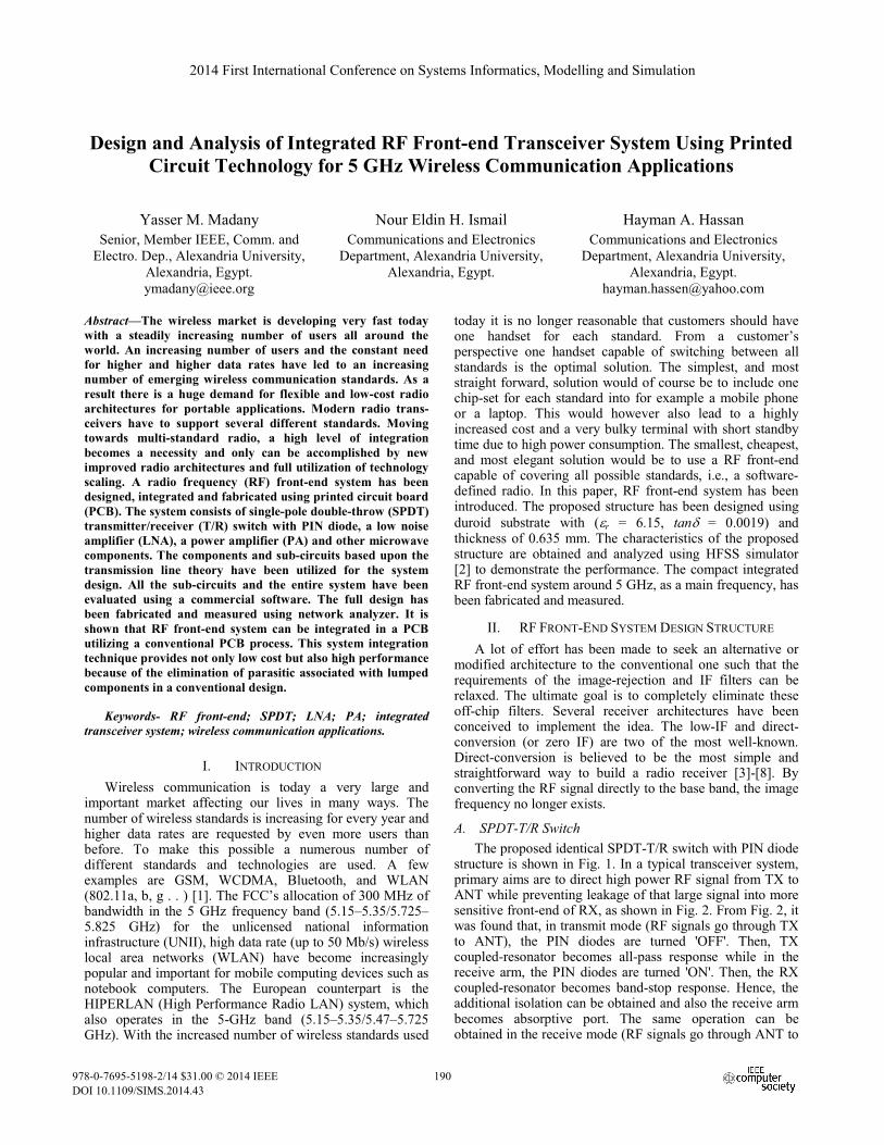
B. SPDT-T/R Switch Quadrature hybrids or hybrid couplers are well known
devices used for their ability to generate signals 90° out of phase at its outputs. The port closer to the input port is
leading in phase by 90°. The port located on the same side as the input port is isolated since there is no power reaching it, as shown in Fig. 4. The hybrid coupler can act as a phase shifter to provide the necessary 90° characteristics to operate with I/Q signal for direct conversions [14].
Figure 4. The hybrid coupler structure and S-parameters result.
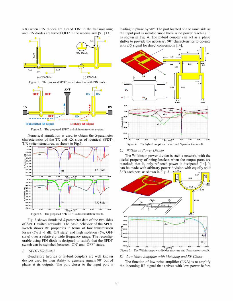
C. Wilkinson Power Divider The Wilkinson power divider is such a network, with the
useful property of being lossless when the output ports are matched; that is, only reflected power is dissipated [14]. It can be made with arbitrary power division with equally split 3dB each port, as shown in Fig. 5.
Figure 5. The Wilkinson power divider structure and S-parameters result.
D. Low Noise Amplifier with Matching and RF Choke The function of low noise amplifier (LNA) is to amplify
the incoming RF signal that arrives with low power before
1.00 2.00 3.00 4.00 5.00 6.00 7.00 8.00 9.00 10.00Freq [GHz]
-50.00
-45.00
-40.00
-35.00
-30.00
-25.00
-20.00
-15.00
-10.00
-5.00
0.00
S-Pa
ram
eter
s [dB
]
g ANSOFT
S21
S11
TX-Side
1.00 2.00 3.00 4.00 5.00 6.00 7.00 8.00 9.00 10.00Freq [GHz]
-50.00
-45.00
-40.00
-35.00
-30.00
-25.00
-20.00
-15.00
-10.00
-5.00
0.00
S-Pa
ram
eter
s [dB
] S11
S21 RX-Side
S12
S13
S11
S14
S13
S12
S11
191191191

LNA Chip Location
Input Output
LNA with Matching Networks RF Chock
Output
RF Chock
Input
PA with Matching
Double stage PA
Single stage PA
PA Chip Location
the consecutive stages add more noise, provided that the LNA adds very little noise itself. It should be placed as close to the antenna as possible in order to have the highest signal possible. The LNA chip used is from Avago (MGA-665P8). Fig. 6 shows the LNA together with the distributed input and output matching networks and RF choke. Also, the S-parameters simulation result has been obtained. RF choke is composed of a radial stub for RF-������ �� �� �� �transmission line to transfer RF-short at the radial stub to RF-open at the LNA output.
Figure 6. The LNA with matching networks and RF chock structures and S-parameters result
E. Power Amplifier with Matching and RF Choke The power amplifier (PA) provides the necessary gain,
minimum RF loss and undesired interaction among the RF signals in order to fulfill this requirement. It is the most critical active component in transmission. The PA chip used is from Avago (MGA-83563). Fig. 7 shows the double stage PA together with the distributed input and output matching networks and RF choke. The S-parameters simulation result has been obtained.
Figure 7. The double stage PA with matching networks and RF chock structures and S-parameters result.
F. RF Front-end Transceiver System The proposed system consists of SPDT-T/R switch with
PIN diode, a LNA, a double stage PA and other microwave components, such as hybrid coupler, power divider, antenna feed transmission line and matching networks to adapt the system with desired frequency, as shown in Fig. 8. The mechanical parameters in millimeter have been shown in Fig. 8 while the rest parameters remain as mentioned before.
Figure 8. The proposed RF front-end transceiver system design structure.
Fig. 8 shows the signal flow graph to analyze the S-parameters characteristics of the proposed design structure, as shown in Fig. 9.
(a) S-parameters in dB.
S12
S11
High Isolation Up to -75 dB
S11
S12
High Isolation Up to -85 dB
Transmitting Section Receiving Section
Input Carrier Signal
Input Carrier Signal to Hybrid
Input Carrier
Signal to PA Detected
Signal Matched Load
Rx Signal from LNA Tx Signal
from PA
Antenna
Port 2
Port 3 Port 1
S12
S13 S11
192192192

(b) Surface current density, Jsur. Figure 9. The proposed RF front-end transceiver system simulation
results.
III. THE INTEGRATED RF FRONT-END TRANSCEIVER SYSTEM EXPERIMENTAL MEASUREMENTS
Photograph of the proposed fabricated miniaturized integrated RF Front-end Transceiver System structure at antenna laboratory is shown in Fig. 10. The measured S-parameters in dB of the proposed structure can be analyzed with network analyzer HP8719ES, as shown in Fig. 11.
(a) Without LNA and PA chips.
(b) With LNA and PA chips. Figure 10. The proposed fabricated proposed RF front-end transceiver
system at antenna Laboratory.
(a) Without LNA and PA chips.
(b) With LNA and PA chips. Figure 11. The measured S-parameters in dB of the proposed fabricated
proposed RF front-end transceiver system.
From measured S-parameters, f= 5�0.15 GHz, at antenna laboratory, as shown in Fig. 11(a), it was found that the input port (port 1), antenna (port 2) and detected signal (port 3) have analyzed. Hence, from reference [14], for transmitting side, the input port return loss (RL), S11= -24 dB and the S-parameter between port 1 and port 2, S21= -58 dB,
S11[dB] = 20 log (r), then r = 0.063
Power transmitted = [1-(r)2]�100 = 99.6%
S21[dB] = 20 log (r), then r = 0.00126
The gain = [1-(r)2]�100 = 99.999%
and for receiving side, the return loss (RL), S22= -17.6 dB and the between port 2 and port 3, S32= -37 dB,
S22[dB] = 20 log (r), then r = 0.132
Power received = [1-(r)2]�100 = 98.3%
S32[dB] = 20 log (r), then r = 0.0141
The gain = [1-(r)2]�100 = 99.999%
From Fig. 11(b), a narrow view at the frequency band 4.8-5.2 GHz with LNA and PA chip has been illustrated. It was found that the measured S11 for Tx mode result has been differed slightly than the measured S11 for Rx mode result because of the effect of practical design accuracy according to the design structure complexity, connectors and element chips (LNA and PA) welding. But, the measured Tx mode and Rx mode results have been shared the frequency band for S11 ��-10dB.
IV. CONCLUSIONS The revolutionary advances in integrated circuits (ICs)
have brought the world of wireless communications into a completely new era. System-on-chip (SOC) is no longer a dream. New technologies acting as a driving force have pushed the personal wireless communications market into today’s boom. The market motivates low-cost, low-power and high performance circuit designs. To meet these requirements, communication system considerations and transceiver architecture innovations play a most essential role. In this paper, the design and analysis of fully integrated
LNA
PA PA
-6 dB -10 dB
193193193
RF front-end transceiver system is described using printed circuit technology. The proposed system architecture and circuit design issues are discussed and a prototype is built and fabricated. The measured results have a good agreement with simulated results to introduce an integrated and miniaturized RF front-end transceiver system (6.9cm×4.3cm) at 5 GHz with SPDT-T/R switch, double stage PA and LNA. The proposed system has achieved excellent performance due to the elimination of parasitic associated with lumped components in a conventional design with 99.6% power transmitted, 98.3% power received and 99.999% gain in both transmission and receiving sides to meet the requirements of 5 GHz wireless communication applications, such as the unlicensed 5 GHz band (802.11a/n). The presented work shows the possibilities of designing flexible RF front-ends for wireless transceivers using RF-sampling technique and printed circuit technology.
REFERENCES [1] M. Vidojkovic, J. van der Tang, P. Baltus, and A. van Roermund,
“Design of Flexible RF Building Blocks—A Method for Implementing Configurable RF Tranceiver Architectures,” in Proc. of Asia-Pacific Conference on Communications, pp. 445–449, 2005.
[2] “High frequency structure simulator software package,” HFSS v12.l, Ansoft Corporation.
[3] S. Gong, A. Backstrom, M. Agesjo, A. Serban, M. Karlsson, "Integration of a 5-GHz radio front-end in PCB," High Density Microsystem Design and Packaging and Component Failure Analysis, 2006. HDP'06. Conference on , pp.146,148, 27-28 June 2006.
[4] E. Laskin, A.Tomkins, A. Balteanu, I. Sarkas, and S.P. Voinigescu,“A 60-GHz RF IQ DAC Transceiver With On-Die At-Speed Loopback,” IEEE Radio Frequency Integrated Circuits Symposium (RFIC), 2011.
[5] M.Y.W. Chia, C.K. Ang, B. Luo, S.W. Leong,“Wideband 307 GHz Transceiver System For High Speed Digital Wireless at 12.5 Gbps,” IEEE MTT-S Inter. Microwave Symposium Digest (MTT), 2011.
[6] P. Philippe and A. Oruk, “A highly miniaturized 2.4 GHz Bluetooth radio module utilizing an advanced system in package technology”, Proc. of European conf. on Wireless Technology, pp. 169-172, 2004.
[7] S. Gong, M. Karlsson and Adriana Serban, “Design of a radio front-end module at 5 GHz”, Proc. of IEEE 6th Circuits and System Symposium on Emerging Technologies, p.241-244, 2004.
[8] Y.M. Madany, and A.A. Salama, "Design and analysis of miniaturized integrated antenna with direct conversion transceiver for wireless communications applicaions," Microwave and Millimeter Wave Technology (ICMMT), Inter. Conf. on , vol.5, pp.1-4, May 2012.
[9] Y.M. Madany, N.E.H. Ismail, and H.A. Hassan, “Analysis and Design of Wideband Single-Pole Double-Throw (SPDT) Transmitter/Receiver (T/R) Switch with PIN Diode for Transceiver Systems,” IEEE Inter. Symp. on Antennas and Propagation and USNC/URSI National Radio Science Meeting (APS'2013), pp. 1004-1005, July 2013.
[10] Y.M. Madany, N.E.H. Ismail, and H.A. Hassan, “High-Isolation Wideband Single-Pole Double-Throw (SPDT) Transmitter/Receiver (T/R) Switch with PIN Diode for Wireless Communication Applications,” IEEE Inter. Symp. on Antennas and Propagation and USNC/URSI National Radio Science Meeting (APS'2013), pp. 1006-1007, July 2013.
[11] Y.Ushijima, E.Nishiyama, and M.Aikawa,“Single layer extensible microstrip array antenna integrating SPDT switch circuit for linear polarization switching,” IEEE Transactions on Antennas and Propagation, vol. 60, no. 11, November 2012.
[12] S.Y.M.J.Hamzah, B.H.Ahmad, and P.W.Wong,"Multiband matched bandstop filter," Proceedings of 2010 IEEE Asia-Pacific Conference on Applied Electromagnetics (APACE 2010), pp.1-4, November 2010.
[13] M.K.Zahari, B.H.Ahmad, N.A.Shairi, and P.W.Wong; ,"Reconfigurable matched bandstop filter," RF and Microwave Conference (RFM), 2011 IEEE International, pp.230-233, December 2011.
[14] D.M. Pozar, “Microwave engineering”, JohnWiley & Sons, Inc, 4th edition, 2012.
194194194