Darabi Integraded RF Front End
13
2038 IEEE TRANSACTIONS ON CIRCUITS AND SYSTEMS—I: REGULAR P APERS, VOL. 58, NO. 9, SEPTEMBER 2011 Highly Integrated and Tunable RF Front Ends for Reconfigurable Multiband Transceivers: A Tutorial Hooman Darabi, Ahmad Mir zaei, and Mohy ee Mikhema r Abstract—Architectural and circuit techniques to integrate the RF front end passive components, namely the SAW filters and du- plexers that are traditionally implemented off chip, are presented. Inte nded fo r soft war e-de fined and cog nitiv e radi o platf orms , tunable high-Q filters realized by CMOS switches and linear or MOS capa cito rs allo w the integ rati on of highl y rec onfig urab le transceiver front ends that are robust to in-band and out-of-band blockers. Furthermor e, duplexer techniques based on electrical balance concepts are introduced to enable highly integrated and programmable radios for full-duplex applications such as 3/4G transceivers. Several case studies are presented that offer highly linear and low-noise transceiver front ends that satisfy the chal- lenging requirements of cellular standards, yet offer considerably lower cost and size compared to the state-of-the-art transceivers availa ble today. Index Terms—Cellular , duplexers, EDGE, electrical balance, fil- ters, fre quency divis ion duple xing , fre quency sele ctiv ity , fro nt end, GSM, passive, quality factor , SA W filters, softwar e-defined radios, WCDMA. I. INTRODUCTION T HE RECENT demand on instant and wideband access to inf ormation and communica tion req uir es a mobile ter minal that is cap able of del iveri ng the ult ima te use r ex- perie nce. One realiz ation is a softw are-d efined radio (SDR) [1]–[3], [47], which is a highly programmable device that is reconfigured through software to operate over a wide range of carrie r freque ncies and chann el bandw idths . If desig ned properly, the SDR is capable of transforming itself, satisfying the requirements of any specified standard at competitive powe r consumpti on, size, and flexibi lit y. One common exa mpl e of the SDR is 3G cell phones, which allow as many as 17 bands in three modes of operation, that is, GSM, EDGE, and WCDMA/HSPA. The first SDR architecture was proposed by Mitola [1], in which the RF and analog processing are reduced to only a pair of data converters, as shown in Fig. 1(a), thus providing the maximum flexibility and programmability through the digital proce ssing block . This ideal istic approa ch howeve r, suf fers from a fundamental limitation; that is, the poor tolerance of such a rad io to t he int erf ere rs. Sho wn in Fig . 2, i n man y wireless applications, a small desired signal could be accompanied by Manuscript received March 01, 2011; revised April 22, 2011; accepted June 30, 2011. Date of current version September 14, 2011. This paper was recom- mended by Associate Editor H. Luong. The authors are with the Broadcom Corporation, Irvine CA 92617 USA (e-mail: hdarabi@broadco m.com). Color versions of one or more of the figures in this paper are available online at http://ieeexp lore.ieee.org. Digital Object Identifier 10.1109/TCSI.2011.216 2460 Fig. 1. (a) Ideal SDR . (b) A more practical archi tectu re. Fig. 2. Blockers in wireless en vironments. several large in-band (created due to nearby transmitters of the same communication standard), or out-o f-band blockers (caused by any transmitter). At times, these blockers could be as much as about 100 dB larger than the desirable received signal, which, due to the lack of any filtering in the SDR of Fig. 1(a), would demand an impractical dynamic range of about 100 dB on the ADC. According to the survey published in [4], this demand leads to an unacceptable power dissipation of 2 kW estimated for the ADC! That is three orders of magnitudes higher than what a cellular power amplifier (PA) could con- sume. Thus, a more practical receiver architecture shown in Fig. 1(b) is adopted in most SDRs today [3], [47], where, by means of downconversion, a considerable portion of analog and digital signal processing is performed at a conveniently lower intermed iate fre quenc y (IF). The diff ere nce from the other traditional radios is the added programmability in almost everything, including channel-select filter bandwidth or ADC sample rate to allow several modes of operation, as well as extended RF bandwidth of the transceiver front end and PLL range to support multiple bands. Even though the architecture of Fig. 1(b) solves the in-band blocker problem through programmable IF filtering, the out-of- band blockers remain a challenge. In the case of GSM for ex- ample, a 0 dBm out-of-band blocker can heavily compress the receiver front end (explained more in Section II and Fig. 3), and thus desensitize it. Therefore, an additional front-end filter is needed to suppress the blocker adequately [Fig. 1(b)] before 1549-8328/$26.00 © 2011 IEEE
Transcript of Darabi Integraded RF Front End

7/21/2019 Darabi Integraded RF Front End
http://slidepdf.com/reader/full/darabi-integraded-rf-front-end 1/13
2038 IEEE TRANSACTIONS ON CIRCUITS AND SYSTEMS—I: REGULAR PAPERS, VOL. 58, NO. 9, SEPTEMBER 2011
Highly Integrated and Tunable RF Front Ends forReconfigurable Multiband Transceivers: A Tutorial
Hooman Darabi, Ahmad Mirzaei, and Mohyee Mikhemar
Abstract—Architectural and circuit techniques to integrate theRF front end passive components, namely the SAW filters and du-plexers that are traditionally implemented off chip, are presented.Intended for software-defined and cognitive radio platforms,tunable high-Q filters realized by CMOS switches and linear orMOS capacitors allow the integration of highly reconfigurabletransceiver front ends that are robust to in-band and out-of-bandblockers. Furthermore, duplexer techniques based on electricalbalance concepts are introduced to enable highly integrated andprogrammable radios for full-duplex applications such as 3/4Gtransceivers. Several case studies are presented that offer highlylinear and low-noise transceiver front ends that satisfy the chal-lenging requirements of cellular standards, yet offer considerably
lower cost and size compared to the state-of-the-art transceiversavailable today.
Index Terms—Cellular, duplexers, EDGE, electrical balance, fil-ters, frequency division duplexing, frequency selectivity, front end,GSM, passive, quality factor, SAW filters, software-defined radios,WCDMA.
I. INTRODUCTION
THE RECENT demand on instant and wideband access
to information and communication requires a mobile
terminal that is capable of delivering the ultimate user ex-
perience. One realization is a software-defined radio (SDR)[1]–[3], [47], which is a highly programmable device that is
reconfigured through software to operate over a wide range
of carrier frequencies and channel bandwidths. If designed
properly, the SDR is capable of transforming itself, satisfying
the requirements of any specified standard at competitive power
consumption, size, and flexibility. One common example
of the SDR is 3G cell phones, which allow as many as 17
bands in three modes of operation, that is, GSM, EDGE, and
WCDMA/HSPA.
The first SDR architecture was proposed by Mitola [1], in
which the RF and analog processing are reduced to only a pair
of data converters, as shown in Fig. 1(a), thus providing themaximum flexibility and programmability through the digital
processing block. This idealistic approach however, suffers
from a fundamental limitation; that is, the poor tolerance of
such a radio to the interferers. Shown in Fig. 2, in many wireless
applications, a small desired signal could be accompanied by
Manuscript received March 01, 2011; revised April 22, 2011; accepted June30, 2011. Date of current version September 14, 2011. This paper was recom-mended by Associate Editor H. Luong.
The authors are with the Broadcom Corporation, Irvine CA 92617 USA(e-mail: [email protected]).
Color versions of one or more of the figures in this paper are available onlineat http://ieeexplore.ieee.org.
Digital Object Identifier 10.1109/TCSI.2011.2162460
Fig. 1. (a) Ideal SDR. (b) A more practical architecture.
Fig. 2. Blockers in wireless environments.
several large in-band (created due to nearby transmitters of
the same communication standard), or out-of-band blockers(caused by any transmitter). At times, these blockers could be
as much as about 100 dB larger than the desirable received
signal, which, due to the lack of any filtering in the SDR of
Fig. 1(a), would demand an impractical dynamic range of about
100 dB on the ADC. According to the survey published in [4],
this demand leads to an unacceptable power dissipation of 2
kW estimated for the ADC! That is three orders of magnitudes
higher than what a cellular power amplifier (PA) could con-
sume. Thus, a more practical receiver architecture shown in
Fig. 1(b) is adopted in most SDRs today [3], [47], where, by
means of downconversion, a considerable portion of analog
and digital signal processing is performed at a conveniently
lower intermediate frequency (IF). The difference from theother traditional radios is the added programmability in almost
everything, including channel-select filter bandwidth or ADC
sample rate to allow several modes of operation, as well as
extended RF bandwidth of the transceiver front end and PLL
range to support multiple bands.
Even though the architecture of Fig. 1(b) solves the in-band
blocker problem through programmable IF filtering, the out-of-
band blockers remain a challenge. In the case of GSM for ex-
ample, a 0 dBm out-of-band blocker can heavily compress the
receiver front end (explained more in Section II and Fig. 3), and
thus desensitize it. Therefore, an additional front-end filter is
needed to suppress the blocker adequately [Fig. 1(b)] before
1549-8328/$26.00 © 2011 IEEE

7/21/2019 Darabi Integraded RF Front End
http://slidepdf.com/reader/full/darabi-integraded-rf-front-end 2/13
DARABI et al.: HIGHLY INTEGRATED AND TUNABLE RF FRONT ENDS 2039
the large gain of the low noise amplifier (LNA) occurs. The
filter typically requires a narrow bandwidth set by a given ap-
plication and a very sharp stop-band. Consequently, due to its
very high-quality nature, it is typically implemented externally,
which adds considerably to the cost and size of the reference
design.
Moreover, because the filter bandwidth and center frequencyare inevitably not programmable, for every band or mode of op-
eration, a dedicated input and its corresponding filter are needed.
These items further add to the cost, and more importantly, op-
pose the promise of maximum hardware sharing offered by the
SDR architecture shown in Fig. 1(b). This circumstance con-
tinues to be one of the greatest obstacles to realizing true soft-
ware-defined radios.
In this paper, we introduce several circuit techniques to ad-
dress this great challenge, enabling highly programmable and
tunable front-end filters and duplexers integrated along with the
rest of the CMOS RF IC. The paper is organized as follows:
Section II provides more details of system level requirements of
the radio front end. The main focus is on cellular applications,which are the most challenging realization of SDR. Sections III
and IV are dedicated to 2G and 3G receivers, followed by a
discussion of transmitters in Section V. Duplexer techniques
are described in Section VI, and conclusions are presented in
Section VII.
II. FRONT-END INTEGRATION CHALLENGES AND SYSTEM
REQUIREMENTS
In this section, we discuss the challenges and high-level re-
quirements of the integration of the SAW filters for 2/3G trans-
ceivers. Because cellular is the most demanding wireless stan-dard with regard to filtering, we mostly focus on that.
As shown in Fig. 3, in a GSM receiver, a weak desirable signal
3 dB above the reference sensitivity ( dBm or 2.5 V) and
as close as 20/80 MHz to the desirable signal at the edge of the
band is specified for low/high band cases, to be accompanied by
very large in-band and out-of-band blockers (as large as 0 dBm).
Thus, for the case of a GSM/EDGE receiver, the main require-
ment arises from the radio tolerance to the 0 dBm blocker. The
blocker is a static sine wave and imposes only compression is-
sues.
Knowing that the in-band blockers (subject to almost no RF
filtering) are as large as dBm at 3 MHz away (Fig. 3), theRF filter needs to provide at least 23 dB (approximately) of at-
tenuation on the out-of-band blocker to reduce it to the level that
the RX front end can handle. If realized by inductors and capac-
itors, the corresponding quality factor (Q) would be greater than
100, thus making it impractical to be realized on-chip, and es-
pecially in a regular bulk CMOS process.
Note that even though a sensitivity of dBm is speci-
fied in the standard, most advanced handsets today target for
dBm sensitivity or better, which translates to a total noise
figure of 5 dB for the entire system (assuming 200 kHz band-
width and 5 dB signal-to-noise ratio or SNR). With a 1 dB loss
budget for the switch and 1.5 dB for the SAW filter, the re-
ceiver noise figure must be about 2.5 dB. On the other hand,a SAW-less receiver can enjoy a higher noise figure of 4 dB to
Fig. 3. GSM out-of-band blocker profile.
Fig. 4. GSM Noise requirement in RX band.
Fig. 5. Direct-conversion TX versus translational loop.
achieve the same sensitivity as the 1.5 dB loss of the filter is
eliminated.
For a GSM transmitter, an output noise of less than dBm
(measured at a 100 kHz resolution bandwidth at the corre-
sponding receive-band) is needed to ensure that the nearby
receiver is not desensitized by the other handset transmitting atfull power (Fig. 4). Given that the edge of the RX band starts at
20 MHz away for low bands, the required system phase noise
at dBm output power is
dBm kHz dBm
Excluding the PA noise (which is typically dBm and
better than dBm worst case), the radio contribution must
be less than dBc Hz at 20 MHz. To meet this challenging
requirement without any external filtering, the GSM transmit-
ters traditionally have been using translational loops [5], [7] or
direct modulated PLLs [6], [8], [9], [36], which could be ex-tended to a polar scheme in the case of EDGE [7]–[12], [36],
[41]–[44] that supports 8PSK modulation (see Fig. 5). The ad-
vantage of these architectures is that the noise of the IQ modu-
lator [39] (a substantial noise contributor) is eliminated. In the
case of a translational loop for instance, the PLL forces the VCO
output to be a replica of the modulated input spectrum fed to
the phase frequency detector (PFD), thus translating the inter-
mediate frequency (IF) spectrum to radio frequency (RF). Here,
unlike the direct-conversion case, only the VCO and LO chain
contribute to the far-out noise (the PLL bandwidth is usually
narrow enough to suppress the noise of the rest of the loop).
Moreover, because the VCO and PA output have exactly the
same phase content, this type of transmitter is more immune topulling.
7/21/2019 Darabi Integraded RF Front End
http://slidepdf.com/reader/full/darabi-integraded-rf-front-end 3/13
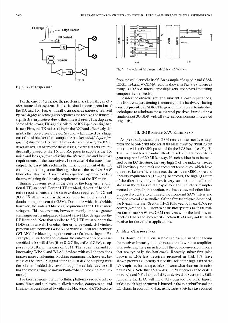
2040 IEEE TRANSACTIONS ON CIRCUITS AND SYSTEMS—I: REGULAR PAPERS, VOL. 58, NO. 9, SEPTEMBER 2011
Fig. 6. 3G Full-duplex issue.
For the case of 3G radios, the problem arises from the full-du-
plex nature of the system, that is, the simultaneous operation of
the RX and TX (Fig. 6). Ideally, an external duplexer realized
by two highly selective filters separates the receive and transmit
signals, but in practice, due to the finite isolation of the duplexer,
some of the strong TX signals leak to the RX input, causing two
issues: First, the TX noise falling in the RX band effectively de-
grades the receive noise figure. Second, when mixed by a large
out-of-band blocker (for example the blocker at half-duplex fre-
quency) due to the front-end third-order nonlinearity the RX is
desensitized. To overcome these issues, external filters are tra-
ditionally placed at the TX and RX ports to suppress the TX
noise and leakage, thus relaxing the phase noise and linearity
requirements of the transceiver. In the case of the transmitter
output, the SAW filter relaxes the noise requirement of the TX
chain by providing some filtering, whereas the receiver SAWfilter attenuates the TX residual leakage and any other blocker,
thereby relaxing the linearity requirements of the RX chain.
Similar concerns exist in the case of the long term evolu-
tion (LTE) standard. For the LTE standard, the out-of-band fil-
tering requirements are the same as those required for 2G and
3G ( dBm, which is the worst case for LTE, is still the
dominant requirement for GSM). Due to the wider bandwidth,
however, the in-band blocking requirement for LTE is more
stringent. This requirement, however, mainly imposes greater
challenges on the integrated channel-select filter design, not the
RF front end. Note that similar to 3G, LTE must support the
FDD option as well. For other shorter-range standards [wirelesspersonal area network (WPAN) or wireless local area network
(WLAN)] the blocking requirements are far less stringent. For
example, in Bluetooth applications, the out-of-band blockers are
specified to be dBm (from 0–2 GHz, and GHz), as op-
posed to 0 dBm in the case of GSM. The recent demand for
integrating WPAN and WLAN devices with cell phones does
impose more challenging blocking requirements, however, be-
cause of the large TX signal of the cellular device coupling with
the other embedded devices (although the cellular device still
has the most stringent in-band/out-of-band blocking require-
ments).
For these reasons, current cellular platforms use several ex-
ternal filters and duplexers to alleviate noise, compression, andlinearity issues imposed by either the blockers or the TX leakage
Fig. 7. Examples of (a) current and (b) future 3G radios.
from the cellular radio itself. An example of a quad-band GSM/
EDGE tri-band WCDMA radio is shown in Fig. 7(a), where as
many as 10 SAW filters, three duplexers, and several matching
components are needed.
Besides the obvious size and substantial cost implications,
this front-end partitioning is contrary to the hardware sharing
concept provided in SDRs. The goal of this paper is to introduce
techniques to eliminate these external passives, introducing asingle-input 3G SDR with all external components integrated
[Fig. 7(b)].
III. 2G RECEIVER SAW ELIMINATION
As previously stated, the GSM receive filter needs to sup-
press the out-of-band blocker at 80 MHz away by about 23 dB
or more, with a 60 MHz passband for the PCS band (see Fig. 3).
The low band has a bandwidth of 35 MHz, but a more strin-
gent stop band of 20 MHz away. If such a filter is to be real-
ized by an LC structure, the very high Q of the inductor needed
will inevitably require Q enhancement techniques, which have
proven to be insufficient to meet the stringent GSM noise and
linearity requirements [13]–[15]. Moreover, the high Q nature
of the filter inevitably makes it very sensitive to small vari-
ations in the values of the capacitors and inductors if imple-
mented on-chip. In this section, we discuss several other ideas
proposed recently to eliminate the front-end SAW filters and
provide several case studies. Of the few techniques described,
the N-path filtering (Section III-C) followed by linear-LNA re-
ceivers (Section III-F) seem to be the most promising in the real-
ization of true SAW-less GSM receivers while the feedforward
(Section III-B) and mixer-first (Section III-A) may not be as at-
tractive for the cellular applications.
A. Mixer-First Receivers
As shown in Fig. 8, one simple and basic way of enhancing
the receiver linearity is to eliminate the low noise amplifier,
thus reducing the gain in front of the downconversion mixers
that are typically the bottleneck. Recently, mixer-first (also
known as LNA-less) receivers proposed in [16], [17] have
shown promising linearity due to the lack of the high gain of the
LNA upfront, but as expected, still somewhat short on the noise
figure (NF). Note that a SAW-less GSM receiver can tolerate a
more relaxed NF of about 4 dB, as derived in Section II. Still,
removing the LNA will inevitably degrade the noise figure,
unless much higher current is burned in the mixer buffer and theLO chain. In addition to that, using large switches (as required

7/21/2019 Darabi Integraded RF Front End
http://slidepdf.com/reader/full/darabi-integraded-rf-front-end 4/13
DARABI et al.: HIGHLY INTEGRATED AND TUNABLE RF FRONT ENDS 2041
Fig. 8. Mixer-first receiver front end.
Fig. 9. Feedforward blocker cancellation concept.
to improve noise figure) directly connected to the receiver input
causes a potentially large LO-to-RF feed-through.Moreover, the harmonic mixing remains a challenge, as the
LNA-less receiver is quite wideband and provides little filtering
at LO harmonics, although the 8-phase mixing scheme in [17]
substantially helps at the expense of increasing the LO chain
power consumption. Fig. 8 shows an example of a single-ended
8-phase design that inherently removes the and
blockers, although in practice is limited by the mismatches in
the LO phase-generation path.
B. Feedforward Blocker Cancellation
Another approach proposed in [18] keeps the LNA so as not
to compromise the NF at the sensitivity level and relies on feed-forward (FF) cancellation of the blocker at the LNA output, as
illustrated in Fig. 9. A similar approach is also demonstrated in
[51] and [52], while we focus on the architecture proposed in
[18] to provide a case study. The features and properties of the
two feedforward examples ([18], [51], and [54]) are very sim-
ilar.
To distinguish the blocker from the desirable signal, a sharp
notch filter in the feedforward path is required. This is realized
by a frequency translational loop where the low-Q high-pass
filter (HPF) response appears at RF through subsequent down
and up conversion by the same receive LO signal. This leads
to a very sharp RF filter whose center frequency is precisely
controlled by the LO and whose bandwidth is conveniently setby the low-Q low-frequency HPF (Fig. 9).
Fig. 10. Actual realization of feedforward filter.
Fig. 11. FF filter response compared to EPCOS SAW.
Since IQ LO signals are available, the actual filter realization
is shown in Fig. 10 where the feedforward path resembles a
linear time-invariant system whose impulse response is:
, where h(t) is the original HPF response (the
BB response translated to ).
The feed-through of the LO signals to the receiver input is a
potential concern similar to mixer-first approach. In this case
however, due to much better isolation between the LO ports
and the input, the measured LO feed-through is well below the
dBm requirement.
Despite a better NF of 4.2 dB achieved here [18] compared
to the LNA-less approach, this scheme suffers from two issues:
1. The lack of any input filtering imposes relatively chal-lenging linearity on the LNA input devices, thus compro-
mising the NF, limiting it to 4 dB.
2. The inevitable phase and gain mismatch between the main
and FF paths limit the amount of filtering to about low
20 dB as shown in Fig. 11 (black curve). Although this
value is marginally adequate and comparable to a commer-
cial external filters worst case, a higher rejection is helpful.
The latter issue can be alleviated by using adaptation tech-
niques to improve matching at the expense of complexity.
C. N-Path Filtering
Inspired by N-path filtering concept introduced in 1960 [19]and subsequently used in switched capacitor (SC) filters in early

7/21/2019 Darabi Integraded RF Front End
http://slidepdf.com/reader/full/darabi-integraded-rf-front-end 5/13
2042 IEEE TRANSACTIONS ON CIRCUITS AND SYSTEMS—I: REGULAR PAPERS, VOL. 58, NO. 9, SEPTEMBER 2011
Fig. 12. N-path filtering concept.
Fig. 13. Implementation of 4-path filter.
1980s [20], we realized the following alternative approach. Con-
sider the low-pass SC filter of Fig. 12, where a sampling fre-quencyof isapplied. Due tothe Nyquist limit (NY), the max-
imum allowable frequency is , leaving only one replica of
the low-pass response. Now assume we have N replicas of the
same filter, each turning on at th of a period rotating clock-
wise. It can be shown [20] that now the Nyquist limit is extended
by N times, allowing other replicas of the filter response, partic-
ularly the one at , to be extracted.
An example of a 4-path realization is shown in Fig. 13. It
can be shown [21] that, as expected, base-band impedance of
is translated to , in series with the switch resistance,
, where is the 4-phase clock frequency applied to the
switches as illustrated in Fig. 13.To extend the flat region and improve the stop-band rejection,
it is crucial to minimize the switch resistance with respect to the
parasitic impedance at the input of the filter. For typical values
of switch sizes and RF parasitics, a stop-band rejection of up to
20 dB is feasible with one stage of filtering.
Shown in Fig. 14 is the actual circuit implementation of the
4-phase filter, where to minimize noise and linearity, the base-
band impedance is simply reduced to a capacitor .
For applications with wider channel bandwidth, the baseband
impedance may be replaced by a parallel RC.
The BPF is implemented differentially to make it robust
to common-mode noise. In GSM low bands, the out-of-band
blockers can be as close as 20 MHz to the desired signal. Thus,to determine the minimum size of the baseband capacitor ,
Fig. 14. Realization of M-path filtering.
Fig. 15. SAW-less SoC die photo.
the impedance must be low enough to adequately attenuate
the blocker without causing any gain compression. It must be
emphasized that the switches of the BPF carry no dc current,
and thus their noise contribution is minimal. Additionally, a
good linearity of the proposed high-Q BPF is guaranteed, dueto the low-resistance switches offered in submicron CMOS
technologies.
For the proof of concept, a quad-band GSM/GPRS/EDGE
receiver (as part of a 2.5G SoC) with integrated front-end SAW
filters is fabricated [22], [48]. The SoC die photo is shown in
Fig. 15 (the radio is at the upper-left corner). The radio core
occupies about 5 mm in 65 nm CMOS.
Illustrated in Fig. 16 is the SAW-less receiver front-end
circuitry. An on-chip balun converts the single-ended receiver
input from the antenna switch to a differential signal to drive the
inputs of a differential LNA. The secondary of the transformer
is tuned to the desired band, and it ensures a measured of less than dB seen from the input of the RF IC across a
wide range of 1.7–2 GHz for high bands and 0.8–1 GHz for low
bands. This single-ended-to-differential conversion provides a
voltage gain of close to 9 dB as well, resulting in a simulated
receiver noise figure of 2.8 dB. The LNA is a common-source
cascode amplifier, loaded by a differential tuned inductor. To
prevent the saturation of the LNA input devices by the 0 dBm
blocker, an on-chip differential high-Q BPF (the same as the
one shown in Fig. 14) is placed at the inputs. This BPF provides
low-input impedance to far-out blockers without impacting the
desired signal, causing the blockers to be attenuated at this
stage before hitting the LNA.
At this point, the attenuation that the blockers have experi-enced is not enough to cause any significant gain compression

7/21/2019 Darabi Integraded RF Front End
http://slidepdf.com/reader/full/darabi-integraded-rf-front-end 6/13
DARABI et al.: HIGHLY INTEGRATED AND TUNABLE RF FRONT ENDS 2043
Fig. 16. Front-end circuit with high-Q filters.
or intermodulation at the input devices of the LNA. This at-
tenuation, however, is not sufficient for 0 dBm blockers at a
20 MHz offset, which is required for low band. Therefore, asecond high-Q BPF is used at the inputs of the cascode devices.
This additional filtering guarantees that the attenuated blockers
do not cause large swings at the LNA output, although the de-
sired signal experiences the intended amplification by the LNA.
Furthermore, the downconversion current-driven passive mixer,
along with the low-pass response of the transimpedance am-
plifier, is used as the third high-Q BPF. For this purpose, the
switches of the passive mixer must be driven by the same 25%
duty-cycle signal that clock the two other high-Q BPFs. Before
we present the measured results, we briefly discuss some of non-
ideal effects associated with the proposed filtering technique.
D. N-Path Filtering Nonideal Effects
Despite the simplicity of the filter, there are several factors
that must be carefully considered because they can potentially
impact the RX performance. As shown in Fig. 17, a noisy
LO signal driving the switches reciprocally downconverts
the blocker on the top of the desirable signal. Depending
on whether the phase-noise components between four LO
clocks are common-mode or differential,
the downconverted noise components can have various phase
relationships among themselves. To summarize, each capacitor
holds three types of voltages: 1) the downconverted desired
signal at around dc; 2) the downconverted and attenuatedblocker at ; and 3) the reciprocally downconverted
blocker by the LO phase-noise, which is at dc as well. Looking
back from the RF, the first two types are upconverted to the RF
and eventually create RF voltages at the desired and blocker
frequencies, respectively. The third type of capacitor voltages,
however, which are emerged from the LO phase-noise, appear
as an RF noise voltage at around LO, which degrade the receiver
noise figure.
The exact phase noise analysis of the filter is quite cumber-
some and beyond the scope of this paper. Due to its impor-
tance, however, we summarize the final outcome as follows:
For a 0 dBm blocker at a 20 MHz offset, a phase noise of
dBc Hz is shown to create an input-referred noise floor of dBm Hz, assuming everything else is ideal. This noise
Fig. 17. The impact of phase noise.
floor corresponds to a blocker NF of 6.5 dB, which is adequately
below the 15 dB target needed to meet 3GPP [36]. This con-
dition is clearly more stringent than the phase-noise require-
ment of a conventional GSM receiver ( dBc at 3 MHz and
above), and thus the VCO and RX-LO chain are designed prop-
erly to achieve this target.
Another concern arises from the second-order nonlinearity of
the switches. As shown in Fig. 18, assume the switch voltage
has a second-order relation with respect to its current, which is
given as . It can be shown that with
the switches matched, an amplitude-modulated blocker current
of fed to the filter input only creates
a voltage component proportional to , which subsequently
downconverts to around at baseband, causing no issue. A
mismatch of among the switches, however, creates an RF
voltage of , where S(t) is 1 when LO is high,and is 0 when LO is low. This component can now downconvert
on the top of the desirable signal, and hence the switches mis-
matches must be reduced by proper layout techniques. More-
over, the switch 2nd order nonlinearity must be lowered by ap-
plying a sharp LO voltage [53]. It can be shown that by ex-
ploiting common good design and layout techniques, the 2nd
order nonlinearity should not be a major issue for most cases,
including GSM.
The impact of quadrature errors in LO signals driving the
switches is shown in Fig. 19. A mismatch of creates a pro-
portional image component on the opposite side of the desirable
RF voltage, as expected. This component is downconverted,along with the RF signal, falling on top of each other at base-
band, and naturally degrading the SNR. In the case of GSM/
EDGE, a relatively low SNR is needed (about 20 dB for MCS9
EDGE mode which is the most stringent case), thus making the
filter immune to IQ mismatches. Nonetheless, common design
and layout techniques must be used to minimize that.
Similar to LNA-less receivers, the LO harmonic mixing is a
potential issue here, although the relatively narrow bandwidth
of the tuned loads at the LNA input/outputs helps considerably.
In this prototype, a rejection of dB is achieved at ,
which requires only an additional 20 dB of filtering upfront. This
value can be easily achieved, given that the blocker re-
sides at a far frequency of 6 GHz. Alternatively, at the expense of extra power consumption on VCO and the LO path, an M-phase
7/21/2019 Darabi Integraded RF Front End
http://slidepdf.com/reader/full/darabi-integraded-rf-front-end 7/13
2044 IEEE TRANSACTIONS ON CIRCUITS AND SYSTEMS—I: REGULAR PAPERS, VOL. 58, NO. 9, SEPTEMBER 2011
Fig. 18. Second-order nonlinearity in the 4-phase filter.
Fig. 19. Impact of IQ mismatch.
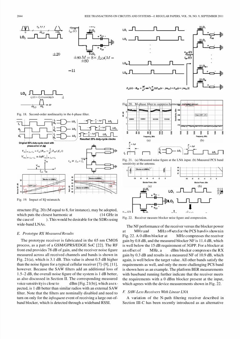
structure (Fig. 20) (M equal to 8, for instance), may be adopted,
which puts the closest harmonic at (14 GHz in
the case of ). This would be desirable for the SDRs using
wide-band LNAs.
E. Prototype RX Measured Results
The prototype receiver is fabricated in the 65 nm CMOS
process, as a part of a GSM/GPRS/EDGE SoC [22]. The RF
front end provides 78 dB of gain, and the receiver noise figure
measured across all received channels and bands is shown in
Fig. 21(a), which is 3.1 dB. This value is about 0.5 dB higher
than the noise figure for a typical cellular receiver [7]–[9], [11],
however. Because the SAW filters add an additional loss of
1.5–2 dB, the overall noise figure of the system is 1 dB better,
as also discussed in Section II. The corresponding measured
voice sensitivityis close to dBm [Fig. 21(b)], which asex-
pected, is 1 dB better than similar radios with an external SAW
filter. Note that the filters are nominally disabled and need to
turn on only for the infrequent event of receiving a large out-of-band blocker, which is detected through a wideband RSSI.
Fig. 20. M-phase filter to suppress harmonic mixing issue.
Fig. 21. (a) Measured noise figure at the LNA input. (b) Measured PCS bandsensitivity at the antenna.
Fig. 22. Receiver measure blocker noise figure and compression.
The NF performance of the receiver versus the blocker power
at MHz and MHz offsetsfor the PCS bandis shownin
Fig. 22. A 0 dBm blocker at MHz compresses the receivergain by 0.8 dB, and the measured blocker NF is 11.4 dB, which
is well below the 15 dB requirement of 3GPP. For a blocker at
an offset of MHz, a dBm blocker compresses the RX
gain by 0.3 dB and results in a measured NF of 10.9 dB, which
again, is well below the target value. All other bands satisfy the
requirements as well, and only the more challenging PCS band
is shown here as an example. The platform BER measurements
with baseband running further indicate that the receiver meets
the requirements with a 0 dBm blocker present at the input,
which agrees with the device measurements shown in Fig. 22.
F. SAW-Less Receivers With Linear LNA
A variation of the N-path filtering receiver described inSection III-C has been recently introduced as an alternative

7/21/2019 Darabi Integraded RF Front End
http://slidepdf.com/reader/full/darabi-integraded-rf-front-end 8/13
DARABI et al.: HIGHLY INTEGRATED AND TUNABLE RF FRONT ENDS 2045
TABLE ISUMMARY OF SAW-LESS RECEIVER APPROACHES
[49], [50] to the multi-stage filtering scheme shown in Fig. 16.
The design features a highly linear LNA, with high supply
voltage to improve the blocker handling, followed by either a
voltage-mode [49] or current-mode passive mixer that provide
the high-Q filtering. The linear LNA enables elimination of the
first two stages of high filters as shown in Fig. 16, but comes at
the expense of somewhat higher power dissipation.
In summary, all three N-path based topologies [48]–[50]
achieve similar noise figure and blocking performance, though
[48] seems to be somewhat lower power as expected. Notethat only [48] features integrated Baluns. Of all the options
presented, the high-Q filtering is the most promising one
(compared to feedforward or mixer-first) as the noise figure at
sensitivity is compromised the least. Moreover, feedforward
techniques unless compensated by some LMS routine, seem to
provide limited filtering. Table I summarizes the main features
of each architecture.
As for a comparison to the receivers with external SAW fil-
ters, There is typically some power penalty, for instance about
5 mA from battery in the case SAW-less RX in [48]. Also the
NF is usually higher, how the overall system NF is less due to
the SAW elimination.
IV. 3G RECEIVER SAW ELIMINATION
In a SAW-less 3G receiver, assuming 45 dB of duplexer isola-
tion and 3 dB of TX insertion loss, the TX leakage at the LNA
input is calculated to be dBm, assuming
full power transmission of 24 dBm at the antenna. This value is
substantially lower than the 0 dBm blocker present in the GSM
case, and also at a further offset frequency of 45 MHz in low
bands, or at least 80 MHz in high bands (as opposed to 20 MHz
in GSM). Depending on duplexer rejection at half-duplex fre-
quency (Fig. 6), an out-of-band of about to 0 dBm is
needed. For instance, for a blocker at half-duplexer frequency
(that is at ), assuming 25 dB of duplexer
filtering, the can be calculated as follows:
where is the blocker power specified to be dBm,
less the 25 dB rejection, the sensitivity for the blocking is
dBm MHz dB, and the SNR is dB, as-
suming a processing gain of 21 dB (or 128). This calculation
leads to an of dBm. This result is obviously a function
of the duplexer isolation and filtering and can vary based on the
platform but is certainly very challenging given that the blocker
can be as close as 22.5 MHz, subject to little filtering in the rel-atively wideband LNA. Similar to the third-order nonlinearity,
Fig. 23. SAW-less 3G RX front-end tolerant to TX leakage.
the receiver second-order nonlinearity amplitude demodulates
the TX leakage and raises the RX noise floor. If no filtering
achieved at the TX frequency, of better than dBm
is typically desirable so as not to affect the receiver sensitivity
considerably. This along with the TX noise (Section V) will
effectively determine the receiver noise figure and adds to
the thermal noise of the receive path alone. Most receivers
today target for 2.5–3 dB of noise figure with additional 0.5–1
dB degradation due to the second-order nonlinearity and the
transmitter noise in the RX band.
The receiver and can be substantially relaxed if
any of the filtering techniques presented in the previous section
are adopted. Alternatively, because the TX leakage is relatively
weak compared to GSM receivers ( dBm versus 0 dBm in
GSM), a simplified front end, such as the one shown in Fig. 23,
can be used where only one stage of filtering at LNA output
is used [23], [25], [26]. The main advantage here is less powerconsumption owing to the fact that the 3G blocker does not im-
pose any compression issue at the LNA input.
Moreover, to save power, the receiver can use 50% of the LO
signals, as opposed to the 25% used in the GSM front end of
Fig. 16 [23]. In the case of 50% LO signal use, however, the
image current circulating between the I and Q branches is trou-
blesome and must be minimized based on the techniques offered
in [23] and [24], which mainly involves the proper choice of ca-
pacitance C and the resonance mode of the LNA RLC load.
V. TRANSMITTER SAW ELIMINATION
As mentioned in Section II, PLL-based TX architectures are
proven to achieve the required phase noise of dBc Hz
at a reasonable power consumption. Thus, as also shown in
Fig. 7(a), all the current GSM/EDGE transmitters are SAW-less
[6]–[12]. In the case of EDGE modulation, because the output
power is 6 dB less (that is, 27 dBm for the low band), the phase
noise accordingly is relaxed to about dBc Hz or better
at a 20 MHz offset. The EDGE transmitter may be built as an
extension of the GSM direct-modulated PLL through a polar
scheme [40]. Alternatively, at the expense of more power con-
sumption, a linear transmitter may be used. Given the 6 dB more
relaxed noise requirement, a direct-IQ (or linear) transmitter
would work reasonably well, although it would be more powerconsuming than what can be achieved in the polar scheme.

7/21/2019 Darabi Integraded RF Front End
http://slidepdf.com/reader/full/darabi-integraded-rf-front-end 9/13
2046 IEEE TRANSACTIONS ON CIRCUITS AND SYSTEMS—I: REGULAR PAPERS, VOL. 58, NO. 9, SEPTEMBER 2011
Fig. 24. Current 3G transmitters.
On the other hand, due to architectural challenges of polar
transmitters [7]–[12], [40] for wide-band modulation transmit-
ters such as 3G, a more straightforward direct-IQ scheme is
adopted [27]–[30], [45], [46], which is noisier due the contribu-
tion of the modulator. This scheme is shown in Fig. 24, wheretypically, the GSM path is using PLL-based architecture to meet
the tight noise requirements, but to overcome the challenges of
the polar scheme, the 3G transmitter is linear [40]. The EDGE
can be either an extension of the PLL-based TX or be run on the
linear 3G portion, as discussed earlier.
To derive the noise requirements of the 3G TX, let us as-
sume a duplexer isolation of 45 dB with 3 dB of insertion loss,
which is common for most of current front ends. A phase noise
of dBc Hz at the transmitter output (excluding the PA)
leads to a noise floor of dBm Hz.
If the RX has a thermal noise figure of 2.5 dB, this condition
effectively degrades the sensitivity by about 0.5 dB, which isacceptable in most designs. The power amplifier noise will add
to this further. Meeting this phase noise target is practical, al-
though not easy, as demonstrated in [27]–[29], provided that the
phase noise of the VCO, the LO chain, and the TX IQ modulator
is properly optimized. A notch filter in the TX path can lower
the power consumption further (if one chooses to use one) [30],
although the transmitters presented in [28] and [29] seem to be
adequately low-power. Also, there recently have been alterna-
tive approaches to realize true multimode 3G transmitters using
wideband polar architectures [37], [38]. An example of a multi-
mode GSM/EDGE/WCDMA wideband polar transmitter based
on an analog two-point modulation PLL [37] is shown in Fig. 25.
As the VCO linearity and gain accuracy are crucial to achieve a
wideband all-pass response, an embedded feedback-frequency
locked loop is employed to stabilize the VCO gain and to ensure
robust performance.
VI. DUPLEXER TECHNIQUES
So far we have established several techniques to eliminate the
external SAW filters in both RX and TX in 2G and 3G modes of
operation. The duplexer, which is unique only to 3G radios, is
discussed in this section. As 3G systems are full-duplex (that is,
the TX and RX operate concurrently), a duplexer is needed at the
antenna to isolate (or more importantly, protect) the LNA from
the high-power PA output going to the antenna (Fig. 26). Typi-cally, an isolation of 45–50 dB in the RX band and 45 dB in the
Fig. 25. Wideband polar multimode 3G transmitter.
Fig. 26. Basic duplexer operation.
TX band is common in current platforms. Because modern RF
duplexers rely on frequency-selective filters for isolation, these
stringent requirements prohibit their integration on silicon, par-
ticularly in CMOS. An alternative implementation is based on
the electrical balance [33] of a hybrid transformer rather than
frequency selectivity, which unfavorably requires high-Q ele-
ments. This concept, along with a prototype duplexer, is dis-cussed next in more detail.
A. Electrical Balance Concept
An integrated duplexer should perform two functions: first,
it must provide concurrent matching for the antenna, the trans-
mitter, and the receiver, and second, it should attenuate the trans-
mitted signal at the RX input to avoid saturation or desensiti-
zation. The solution to this challenge was introduced some 90
years ago for old telephony systems, relying on a class of net-
works called maximum output networks [31].
In a telephone handset, the weak received signal from the
switching office should be isolated from the strong locally gen-erated microphone signal; otherwise, listeners will be deafened
by their own voices. The isolation was implemented using
the hybrid transformer shown in Fig. 27. When the balancing
resistor is identical to the switching office line resistance
, the microphone current experiences identical loads (the
same inductors and resistors are used). Therefore, identical
voltage waveforms are formed on the line and the balancing
resistor. Thus, the microphone voltage shown in black appears
as common-mode and does not create a voltage across L2.
On the other hand, the PSTN current (in grey), experiences a
single-ended circuit and couples to the speaker with the voltage
gain of the hybrid transformer.
A well-known embodiment of the hybrid transformer (HT) asan RF duplexer is shown in Fig. 28 [32], [33]. The HT has sev-

7/21/2019 Darabi Integraded RF Front End
http://slidepdf.com/reader/full/darabi-integraded-rf-front-end 10/13
DARABI et al.: HIGHLY INTEGRATED AND TUNABLE RF FRONT ENDS 2047
Fig. 27. Electrical balance in a telephone handset.
Fig. 28. Electrical balance in modern 3G transceivers.
eral peculiar characteristics: First, all HT ports can be simultane-
ously matched; second, HT ports are bi-conjugate (TX and RX
are electrically isolated from each other, as are the antenna and
balancing resistor ); and third, the incoming power from
one port can be split in any ratio between the two receiving ports.
The HT shown in Fig. 28 is a balun with three ports connected
and matched to the RX, TX, and antenna. The fourth port, which
is the center tap, is connected to the balancing resistor .
For the ideal balun to operate as a HT, the values of the port re-sistance should satisfy the following requirements:
Once all ports are matched, the balance is achieved, and the TX
and the RX are perfectly isolated. The isolation is merely a func-
tion of the matching between the antenna and the balancing re-
sistor, and thus, ideally, is frequency-independent. This condi-
tion, which is unlike the external duplexers that rely on selec-tivity, can be implemented on-chip, where good resolution and
matching can be achieved.
B. Prototype Implementation
For proof of concept, a prototype duplexer for 3/4G applica-
tions based on the HT in Fig. 28 is implemented (Fig. 29) [34].
At balance, there is no net differential voltage across the balun,
and so zero self-inductance current flows. The duplexer is bal-
anced when the voltage at the antenna port is equal to that at
the balancing network. Consequently, the TX signal appears as
common-mode and does not create a voltage across the LNA
input inductor. This scheme yields an isolation bandwidth (thebandwidth where isolation remains better than 50 dB) of better
Fig. 29. Prototype 3G duplexer.
Fig. 30. Reciprocity in electrical balance duplexers.
than 250 MHz, limited only by pad, bondwire, and other para-
sitics.
As for the performance of the ideal balun, the insertion loss
(IL) is 3 dB for both the TX and the RX. As shown in Fig. 30,
this loss is the result of the reciprocity, which is a character-
istic of any passive network. In other words, if the antenna is
pledged to deliver 100% power to the receiver for zero receiver
insertion loss, so would be the receiver to the antenna. This con-
dition works against delivering the full power from the antennato the TX. Theoretically, half of the power would be wasted,
and in the case of the hybrid transformer, the power would be
dissipated in the fourth terminal (the balancing resistor). Thus,
the electrical balance duplexer suffers from a fundamental 3 dB
loss. A practical balun suffers an additional Ohmic loss, as it is
formed by coupling two separate inductors. Thus, in a mono-
lithic balun, the loss and the coupling trade off with each other.
To reduce the Ohmic loss of the HT, an autotransformer (im-
plemented as a differential inductor) may be used alternatively
[33]. The simplicity of the implementation yields lower loss for
the same coupling, which is about 0.5 dB here.
The transformer could be skewed in favor of the transmitteror the receiver at the expense of degrading one loss for the other.
The transmitter insertion loss versusthat of the receiver is shown
in Fig. 31. At the midpoint, both the RX and TX experience an
ideal loss of 3 dB. The transformer, however, can be skewed to
have fewer turns on the transmitter side (with a ratio of 0.63,
as shown in the example in Fig. 31) to reduce the loss to about
2 dB. This will increase the RX loss, however, to about 4 dB
when matched to 50 . This IL tradeoff potentially present in
the duplexer can be circumvented when we note that the abso-
lute power level at the LNA input is irrelevant to the RX oper-
ation—all that matters is signal-to-noise ratio. In other words,
the RX IL and the effective NF of the duplexer are not neces-
sarily identical, which is not the case for an external SAW du-plexer whose two ports must terminate in 50 . Therefore, in

7/21/2019 Darabi Integraded RF Front End
http://slidepdf.com/reader/full/darabi-integraded-rf-front-end 11/13
2048 IEEE TRANSACTIONS ON CIRCUITS AND SYSTEMS—I: REGULAR PAPERS, VOL. 58, NO. 9, SEPTEMBER 2011
Fig. 31. TX-RX insertion loss trade-off.
Fig. 32. LNA circuit.
Fig. 33. High-power duplexer.
this prototype, the LNA, shown in Fig. 32, is noise-matched by
maximizing the voltage gain that the signal experiences from
the antenna to the LNA input (about 6 dB). Referred to the an-
tenna, the equivalent input voltage noise of the LNA is divided
by this gain. The noise-matched LNA reduces the NF to less
than 1 dB, compared to 3 dB for the LNA in [33]. The achieved
antenna return loss is better than 8 dB, as expected.
C. Full Power Challenges
In 3G TX, the PA should deliver a maximum power of 24dBm to the antenna. For a typical peak-to-average ratio of 3.2
dB, the antenna peak-to-peak voltage swing is about 15 V. The
CMOS resistors, capacitors, and inductors can tolerate the 15 V
swing without breakdown or reliability problems, especially as
no dc current flows in the duplexer. A 65 nm thin-oxide NMOS
switch, however, cannot tolerate this voltage. Instead, a switch
based on stacked FETs with floating well structure [35] may be
used, as shown in Fig. 33.
The full-power duplexer should be codesigned with the PA
to benefit from the inherent 1:2 impedance transformation of
the autotransformer. In this work, we have realized a duplexer
to validate the wideband isolation and the low loss at moderate
signal voltages. To simplify autotransformer design, the LNAwas directly connected across the autotransformer and rejected
Fig. 34. Addressing the antenna mismatch issue.
the common mode at its two input terminals, without the benefit
of the third winding.
D. Antenna Mismatch
Another concern arises from the antenna mismatch, which
could adversely affect the duplexer isolation. As mentioned
earlier, the isolation is achieved when the balancing network
impedance tracks the antenna impedance, but, as the near-field
of the antenna is perturbed, the antenna impedance slowly
changes. The industry specification for acceptable antenna
impedance variation is a voltage standing wave ratio (VSWR)
of 3:1. Therefore, the antenna impedance can lie anywhere
inside the grey circle shown in Fig. 34. The balancing network
impedance can track some variations around the center of the
Smith chart with fine resolution, which is the shaded area in
grey. Note that the antenna impedance variation is very slow
(on the orders of tens of milliseconds or more). The duplexer
isolation can simply monitored at the LNA input and the
balancing network impedance can be corrected accordingly.The antenna tuning unit provides a coarse tuning across the
whole area. The most common implementation for
the antenna tuning unit is a pi network, with an off-chip inductor
and two on-chip capacitor banks (Fig. 34). The main motivation
behind the ATU is to improve the PA efficiency under antenna
mismatch conditions, but we use it here for the duplexer as well.
Note that the duplexer loss is little affected by the antenna
mismatch, and mostly, it is the isolation that will be compro-
mised. This behavior is certainly the opposite of the external
duplexers, which are based on high-Q filtering. Moreover, it is
noteworthy to mention that, in most cases, the transceiver key
requirements (sensitivity being one) are allowed to be relaxedsome in the presence of the antenna mismatch.
E. Prototype Measurement Results
The prototype duplexer is implemented in a 65 nm CMOS
technology, with an active area of less than 0.1 mm and a total
area of 0.2 mm , including the LNA, as shown in Fig. 35[34].
The LNA draws 10 mA from 1.2 V. The balancing network
is designed as an array of switched resistors and capacitors.
The array covers the tuning range over process corners and the
temperature range with a 25% margin. Simulation results in-
dicate that the autotransformer can provide isolation over the
range from 0.5–3 GHz. In this prototype, however, the LNA
covers only the high band from 1.8–2.2 GHz, limited by theload, which, if needed, can easily be extended. The simulated

7/21/2019 Darabi Integraded RF Front End
http://slidepdf.com/reader/full/darabi-integraded-rf-front-end 12/13
DARABI et al.: HIGHLY INTEGRATED AND TUNABLE RF FRONT ENDS 2049
Fig. 35. Prototype duplexer die photo.
Fig. 36. (a) LNA/duplexer cascaded NF. (b) Duplexer isolation.
Fig. 37. TX measured insertion loss.
and measured cascaded NF is 5 dB with a gain of more than 27
dB [Fig. 36(a)]. The simulation and measurement results of the
TX-RX isolation are illustrated in Fig. 36(b), where better than
55 dB of isolation in the TX band and better than 45 dB of iso-
lation in the RX band are achieved.
The measured IL on TX port is better about 2.2 dB and is
shown in Fig. 37.
VII. CONCLUSIONS AND DISCUSSION
Software-defined radios cover several bands and modes of op-
eration through maximum hardware sharing and a wide tuning
range. In all solutions presented so far, however, the lack of in-
tegrated and tunable RF filtering opposes this flexibility. More-
over, there are obvious cost implications due to the external fil-
tering needed. Several circuit-level and architectural techniques
to solve this challenge were presented in this paper. We pro-
posed highly integrated and tunable RF filters for 2G and 3G
receivers, along with architectural schemes to eliminate the in-
termediate SAW filters in 3G transmitters. Tunable integrated
duplexers based on electrical balance prove to be a competi-
tive replacement for the current frequency-selective designs, al-
lowing ultralow cost solutions, with maximum hardware sharingand programmability.
Although techniques proposed here are generic and not fre-
quency- or application-dependent, examples demonstrated here
cover cellular design, which is the most challenging from a
filtering perspective. Both the filtering and electrical balance
schemes work well over a wide range of frequency and could
be used in generic SDRs, up to 6 GHz and beyond.
With the circuit and architectural techniques proposed here,realization of SAW-less radios with integrated duplexers is im-
minent and inevitable.
REFERENCES
[1] J. Mitola, “Cognitive radioarchitecture evolution,” Proc. IEEE , vol.97,no. 4, pp. 626–641, Apr. 2009.
[2] J. Mitola, “The software radioarchitecture,” IEEE Commun. Mag., vol.33, no. 5, pp. 26–38, May 1995.
[3] R. Bagheri et al., “An 800-MHz-6 GHz software-defined wireless re-ceiver in 90-nm CMOS,” IEEE J. Solid-State Circuits, vol. 41, pp.2860–2876, Dec. 2006.
[4] B. Murmann, ADC Performance Survey 1997–2008 [Online]. Avail-able: http://www.stanford.edu/murmann/adcsurvey.html
[5] O. E. Erdogan etal., “A single-chip quad-band GSM/GPRS transceiverin 0.18 m standard CMOS,” ISSCC Dig. Tech. Papers, pp. 318–319,
Feb. 2005.[6] O. Bonnaud et al., “A fully integrated SoC for GSM/GPRS in 0.13 m
CMOS,” ISSCC Dig. Tech. Papers, pp. 482–483, Feb. 2006.[7] R. Pullela et al., “An integrated closed-loop polar transmitter with sat-
uration prevention and low-IF receiver for quad-band GPRS/EDGE,” ISSCC Dig. Tech. Papers, pp. 112–113.
[8] H. Darabi et al., “A quad-band GSM/GPRS/EDGE SoC in 65 nmCMOS,” in VLSI Symp., Jun. 2010, pp. 89–90.
[9] H. Darabi et al., “A fully integrated quad-band GPRS/EDGE radio in0.13 m CMOS,” ISSCC Dig. Tech. Papers, pp. 206–207, Feb. 2008.
[10] J. Mehta et al., “A 0.8 mm all-digital SAW-less polar transmitter in65 nm EDGE SoC,” ISSCC Dig. Tech. Papers, pp. 58–59, Feb. 2010.
[11] G. Puma et al., “Integration of a SiP for GSM/EDGE in CMOS tech-nology,” ISSCC Dig. Tech. Papers, pp. 210–211, Feb. 2008.
[12] M. Elliott et al., “A polar modulator transmitter for EDGE,” ISSCC
Dig. Tech. Papers, pp. 188–189, Feb. 2004.
[13] S. Pipilos etal., “A Si 1.8GHz RLCfilterwithtunable centerfrequencyand quality factor,” IEEE J. Solid-State Circuits, vol. 31, no. 10, pp.1517–1525, 1996.
[14] X. He andW. Kuhn,“A 2.5-GHzlow-power, high dynamic range,self-tuned Q-enhanced LC filter in SOI,” IEEE J. Solid-State Circuits, vol.40, no. 8, pp. 1618–1628, 2005.
[15] W. Kuhn et al., “Dynamic range performance of on-chip RF bandpassfilters,” IEEE Trans Circuits Syst. II, Exp. Briefs, vol. 50, no. 10, pp.685–694, 2003.
[16] M. C. M. Soer et al., “A 0.2-to-2.0 GHz 65 nm CMOS receiver withoutLNA achieving dBm IIP3 and dB NF,” ISSCC Dig. Tech.
Papers, pp. 222–223, Feb. 2009.[17] C. Andrews et al., “A passive-mixer-first receiver with baseband-con-
trolled RF impedance matching, dB NF, and dBm widebandIIP3,” ISSCC Dig. Tech. Papers, pp. 46–47, Feb. 2010.
[18] H. Darabi, “A blocker filtering technique for SAW-less wireless re-ceivers,” IEEE J. Solid-State Circuits, vol. 42, no. 12, pp. 2766–2773,
Dec. 2007.[19] L. Franks and I. Sandberg, “An alternative approach to the realizations
of network functions: N-path filter,” Bell Syst. Tech. J., pp. 1321–1350,1960.
[20] D. V. Grunigen et al., “An integrated CMOS switched-capacitor band-pass filter based on N-path and frequency-sampling principles,” IEEE
J. Solid-State Circuits, vol. SC-18, no. 6, pp. 753–761, 1983.[21] A. Mirzaei et al., “Analysis and optimization of direct-conversion
receivers with 25% duty-cycle current-driven passive mixers,” IEEE
Trans Circuits Syst. I, Reg. Papers, vol. 47, no. 9, pp. 2353–2366,2010.
[22] A. Mirzaei et al., “A 65 nm CMOS quad-band SAW-less receiver forGSM/GPRS/EDGE,” in Proc. VLSI Symp., Jun. 2010, pp. 179–180.
[23] A. Mirzaei, J. Leete, X. Chen, and H. Darabi, “A frequency translationtechnique for SAW-less 3G receivers,” in Proc. VLSI Symp., Jun. 2009,pp. 280–281.
[24] A. Mirzaei et al., “Analysis and optimization of current-driven passivemixers in narrowband direct-conversion receivers,” IEEE J. Solid-State
Circuit , vol. 44, no. 10, pp. 2678–2688, Oct. 2009.

7/21/2019 Darabi Integraded RF Front End
http://slidepdf.com/reader/full/darabi-integraded-rf-front-end 13/13
2050 IEEE TRANSACTIONS ON CIRCUITS AND SYSTEMS—I: REGULAR PAPERS, VOL. 58, NO. 9, SEPTEMBER 2011
[25] D. Kaczman et al., “A single-chip 10-band WCDMA/HSDPA 4-bandGSM/EDGE SAW-less CMOS receiver with DigRF 3G interface and90 dBm IIP3,” IEEE J. Solid-State Circuits, vol. 44,no. 3, pp.718–739,2009.
[26] B. Tenbroek etal., “Single-chip tri-band WCDMA/HSDPA transceiverwithout external SAW filters and with integrated TX power control,”
ISSCC Dig. Tech. Papers, pp. 202–203, Feb. 2008.[27] C. Jones et al., “Direct-conversion WCDMA transmitter with
0
dBc
Hz noise at 190 MHz offset,” ISSCC Dig. Tech. Papers,pp. 336–337, Feb. 2007.[28] Q. Huang et al., “A tri-band SAW-less WCDMA/HSPA RF CMOS
transceiver with on-chip DC-DC converter connectable to battery,” in ISSCC Dig. Tech. Papers, Feb. 2010, pp. 60–61.
[29] X. He et al., “A 45 nm WCDMA transmitter using direct quadraturevoltage modulator with high oversampling digital front-end,” in ISSCC
Dig. Tech. Papers, Feb. 2010, pp. 62–63.[30] A. Mirzaei and H. Darabi, “A low-power WCDMA transmitter with
an integrated notch,” IEEE J. Solid-State Circuits, vol. 43, no. 12, pp.2868–2888, 2008.
[31] G. A. Campbell et al., “Maximum output networks for telephone sub-station and repeater circuits,” Trans. AIEE , vol. 39, 1920.
[32] E. Sartori, “Hybrid transformers,” IEEE Trans. Parts, Mater., Packag.,vol. PMP-4, no. 8, pp. 59–66, Sep. 1968.
[33] M. Mikhemar et al., “A tunable integrated duplexer with 50 dB iso-lation in 40 nm CMOS,” in ISSCC Dig. Tech. Papers, Feb. 2009, pp.
386–387.[34] M. Mikhemar et al., “An on-chip wideband and low-loss duplexer for
3G/4G CMOS radios,” in VLSI Symp., Jun. 2010, pp. 129–130.[35] M. Ahn et al., “A 1.8-GHz 33-dBm P0.1-dB CMOS T/R switch using
stacked FETs with feed-forward capacitors in a floated well structure,” IEEE Trans. Microw. Theory Tech., vol. 57, no. 11, pp. 2661–2670,2009.
[36] H. Darabi et al., “A quad-band GSM/GPRS/EDGE SoC in 65 nmCMOS,” IEEE J. Solid-State Circuits, vol. 46, no. 4, pp. 870–872,Apr. 2011.
[37] M. Youssef, A. Zolfaghari, H. Darabi, and A. Abidi, “A low-powerwideband polar transmitter for 3G applications,” ISSCC Dig. Tech. Pa-
pers, Feb. 2011.[38] Z. Boos et al., “A fully digital multi-mode polar transmitter employing
17b RF DAC in 3G mode,” ISSCC Dig. Tech. Papers, Feb. 2011.[39] H. Darabi and A. A. Abidi, “Noise in RF-CMOS mixers: A simple
physical model,” IEEE J. Solid-State Circuits, vol. 35, no. 1,pp. 15–25,2000.
[40] H. Darabi, H. Jensen, and A. Zolfaghari, “Analysis and design of smallsignal polar transmitters for cellular applications,” IEEE J. Solid-State
Circuits, vol. 46, no. 6, pp. 1237–1249, 2011.[41] Y. Akamine et al., “A polar loop transmitter with digital interface in-
cluding a loop-bandwidth calibration system,” in ISSCC Dig. Tech. Pa-
pers, Feb. 2007, pp. 348–349.[42] R. B. Staszewski et al., “A 24 mm quad-band single-chip GSM radio
with transmitter calibration in 90 nm digital CMOS,” in ISSCC Dig.
Tech. Papers, Feb. 2008, pp. 208–209.[43] A. Hietala, “A quad-band 8PSK/GMSK polar transceiver,” IEEE J.
Solid-State Circuits, vol. 41, no. 5, pp. 1131–1141, 2006.[44] T. Sowlati et al., “Quad-band GSM/GPRS/EDGE polar loop trans-
mitter,” IEEE J. Solid-State Circuits, vol. 39, no. 12, pp. 2179–2189,2004.
[45] M. Cassia et al., “A low-power CMOS SAW-less quad band
WCDMA
HSPA
HSPA
EGPRS transmitter,” IEEE J.Solid-State Circuits, vol. 44, no. 7, pp. 1897–1906, Jul. 2009.
[46] T. Sowlati et al., “Single-chip multi-band WCDMA/HSDPA/HSUPA/ EGPRS transceiver with diversity receiver and 3G DigRF interfacewithout SAW filters in transmitter/3G receiver,” in ISSCC Dig. Tech.
Papers, Feb. 2009, pp. 116–117.
[47] M. Ingels etal., “A 5 mm 40nm LPCMOS transceiver for a software-defined radio platform,” IEEE J. Solid-State Circuits, vol. 45, no. 12,pp. 2794–2806, 2010.
[48] A. Mirzaei et al., “A 65 nm CMOS quad-band SAW-less receiver forGSM/GPRS/EDGE,” IEEE J. Solid-State Circuits, vol. 46, no. 4, pp.950–964, Apr. 2011.
[49] J. Borremans et al., “A 40 nm CMOS highly linear 0.4-to-6 GHz re-ceiver resilient to 0 dBm out-of-band blockers,” in ISSCC Dig. Tech.
Papers, Feb. 2011, pp. 62–64.[50] I. Lu et al., “A SAW-less GSM/GPRS/EDGE receiver embedded in a65 nm SoC,” in ISSCC Dig. Tech. Papers, Feb. 2011, pp. 364–365.
[51] S. Ayazian and R. Gharpurey, “Feedforward interference cancellationin radio receiver front-ends,” IEEE Trans. Circuits Syst. II, Exp. Briefs,vol. 54, no. 10, pp. 902–906, Oct. 2007.
[52] R. Gharpurey and S. Ayazian, “Feedforward interference cancellationin narrow-band receivers,” in Proc. IEEE Dallas/CAS Workshop De-
sign, Appl., Integr. Software, 2006, pp. 67–70.[53] H. Khatri et al., “Distortion in current commutating passive CMOS
downconversion mixers,” IEEE Trans. Microw. Theory Tech., vol. 57,no. 11, pp. 2671–2681, Nov. 2009.
[54] A. Safarian et al., “Integrated blocker filtering RF front-ends,” in Proc.
2007 Radio Freq. Integr. Circuits (RFIC) Symp. , 2007, pp. 13–16.
Hooman Darabi received the Ph.D. degree in elec-trical engineering from the University of California,Los Angeles in 1999.
He is currently a Senior Technical Director withBroadcom Corporation, Irvine, CA. His interests in-clude analog and RF IC design for wireless commu-nications, including Bluetooth, WLAN, and cellularapplications.
Ahmad Mirzaei received the Ph.D. degree in elec-trical engineering from the University of California,Los Angeles, in 2006.
He is currently a Principal Scientist withBroadcom Corporation, Irvine, CA. His interestsinclude analog and RF IC design for wireless com-munications.
Mohyee Mikhemar received the B.S. and M.S. de-grees with honors in electrical engineering from AinShams University, Egypt, in 2000 and 2004, respec-tively, and the Ph.D. degree from the University of California, Los Angeles, in 2009.
Currently, he is a Senior Staff Scientist at the
advanced RF research and development depart-ment with Broadcom Corporation, Irvine, CA. Hisresearch interests include low power multibandand multimode radio design in CMOS, multibandduplexers, and RF filters on silicon and digitally
assisted RF circuits.