
Copyright by Yeonam Yoon 2017
108
Copyright by Yeonam Yoon 2017
Transcript of Copyright by Yeonam Yoon 2017

Copyright
by
Yeonam Yoon
2017

The Dissertation Committee for Yeonam Yoon
certifies that this is the approved version of the following dissertation:
Low-power ADC designs in scaled CMOS process
Committee:
Nan Sun, Supervisor
T. R. Viswanathan
David Z. Pan
Michael Orshansky
Eric Soenen

Low-power ADC designs in scaled CMOS process
by
Yeonam Yoon, B.S.; M.S.
DISSERTATION
Presented to the Faculty of the Graduate School of
The University of Texas at Austin
in Partial Fulfillment
of the Requirements
for the Degree of
DOCTOR OF PHILOSOPHY
THE UNIVERSITY OF TEXAS AT AUSTIN
May 2017

Dedicated to my parents and my wife.

Acknowledgments
Most importantly, I would like to express my very special gratitude to my
supervisor, Prof. Nan Sun. Without his continuous support and insightful guidance,
I would have never accomplished my research works. He has inspired me with
enthusiasm for research. Also, his generosity kept me moving forward. I would
also like to thank my committee members, Prof. T. R. Viswanathan, Prof. David Z.
Pan, Prof. Michael Orshansky, and Dr. Eric Soenen, for their valuable advice and
discussions. I am truly grateful to Dr. Eric Soenen for giving a valuable opportu-
nity for chip fabrication. I have been honored and thankful to my fellow students in
Sun research group: Kareem Ragab, Arindam Sanyal, Long Chen, Wenjuan Guo,
Sungjin Hong, Jeonggoo Song, Xiyuan Tang, Shaolan Li, Miguel Gandara, Linx-
iao Shen, and Abhishek Mukherjee. Special thanks to Arindam Sanyal, Sungjin
Hong, Jeonggoo Song, Long Chen, and Wenjuan Guo for their collaboration in my
research. I am greatly indebted to my parents for their selfless support and care.
Last but by no means least, I am heartily thankful for having my wife, Sojeong Han
in my life. I owe my deepest gratitude to her whose warm encouragement enabled
me to go on with my research.
v

Low-power ADC designs in scaled CMOS process
Yeonam Yoon, Ph.D.
The University of Texas at Austin, 2017
Supervisor: Nan Sun
This thesis presents advanced design techniques for successive approxi-
mation register (SAR) analog-to-digital converters (ADCs), continuous-time ∆Σ
ADCs, and single-slope (SS) ADCs in nano-scale CMOS technologies.
(1) In high-speed SAR ADCs, metastability of the comparator limits the per-
formance, which even results in the sparkle code errors. Proposed background cal-
ibration utilizing the comparator decision time detector removes the metastability-
induced sparkle code errors by controlling the metastability detection window. At
the same time, 1-bit resolution increase is gained from the proposed technique,
which results in the fewer comparison cycles. Along with the relaxed requirement
on the comparator, this cycle reduction helps to achieve the good power efficiency
in high-speed SAR design. A prototype ADC in 40nm CMOS achieves 35.3dB
SNDR and consumes 0.81mW while sampling at 700MS/s.
(2) In the proposed continuous-time∆Σ ADCs, conventional power-hungry
opamp is replaced by voltage controlled oscillators (VCOs) that perform the data
vi

conversion in the phase domain instead of the voltage domain. In contrary to the
opamp which is difficult to achieve good performance in the advanced CMOS pro-
cess, VCOs have many advantages in the phase domain. To solve the nonlinear
gain of VCOs, dual VCO-based integrator is used to suppress the dominant second-
order distortion. To address the distortion from the DAC, a novel DAC calibration
technique that both digitally senses and removes DAC mismatch errors is proposed.
It has low hardware complexity by taking advantage of the intrinsic clocked level
averaging (CLA) capability of dual-VCO-based integrator. It ensures high linearity
regardless of the VCO center frequency. By lowering the VCO center frequency,
power consumption is reduced. A prototype ADC designed in 130nm occupies
an area of only 0.04mm2. It achieves 71dB SNDR over 1.7MHz bandwidth (BW)
while sampling at 250MS/s and consuming only 0.9mW from a 1.2V power supply.
The corresponding figure-of-merit (FOM) is 98 fJ/conversion-step.
(3) A SS ADC has advantages of high linearity and a simple architecture.
Thus, it is well suited for the column-parallel architecture for the CMOS image
sensors. However, conversion speed is severely limited in high-bit resolution since
more than 2N cycles are required for a N-bit resolution. To tackle this limitation, a
two-step approach becomes popular. In this thesis, a two-step SAR/SS architecture
is presented. In addition to reducing the conversion time, analog correlated double
sampling (CDS) can cancel kT/C noise, which enables capacitor area reduction.
A prototype ADC in 180nm CMOS occupies only 9.3µm x 830µm. It achieves
60.5dB SNR after CDS while sampling at 256kHz and consuming 91µW.
vii

Table of Contents
Acknowledgments v
Abstract vi
List of Tables xi
List of Figures xii
Chapter 1. Introduction 1
1.1 Motivation . . . . . . . . . . . . . . . . . . . . . . . . . . . . . . 1
1.2 Organization . . . . . . . . . . . . . . . . . . . . . . . . . . . . . 4
Chapter 2. Sparkle Code Correction and Resolution Enhancement in SAR 6
2.1 Introduction . . . . . . . . . . . . . . . . . . . . . . . . . . . . . 7
2.2 Design of Asynchronous SAR ADC . . . . . . . . . . . . . . . . 10
2.3 Sparkle Code Error . . . . . . . . . . . . . . . . . . . . . . . . . 15
2.3.1 Cause of Sparkle Code Error . . . . . . . . . . . . . . . . 15
2.3.2 Sparkle Code Removal Tachniques . . . . . . . . . . . . 18
2.3.3 Metastability Detection Error Analysis . . . . . . . . . . 20
2.4 Proposed ADC Design . . . . . . . . . . . . . . . . . . . . . . . 22
2.4.1 Design of the 5-b Asynchronous SAR ADC Core . . . . . 22
2.4.2 CDT Quantization and Sparkle Code Removal . . . . . . 23
2.4.3 Choice of τ and 1-bit Resolution Enhancement . . . . . . 25
2.4.4 Background Calibration of the Reference Delay τ . . . . 27
2.4.5 Circuit Implementation . . . . . . . . . . . . . . . . . . . 29
2.5 Measurements . . . . . . . . . . . . . . . . . . . . . . . . . . . . 30
2.6 Conclusion . . . . . . . . . . . . . . . . . . . . . . . . . . . . . 37
viii

Chapter 3. VCO-Based Continuous-Time ∆Σ ADC 40
3.1 Modular Architecture and DAC Calibration . . . . . . . . . . . . 40
3.1.1 Introduction . . . . . . . . . . . . . . . . . . . . . . . . 41
3.1.2 Proposed ADC Architecture . . . . . . . . . . . . . . . . 44
3.1.3 Novel Digital DAC Calibration . . . . . . . . . . . . . . 48
3.1.4 Measurement Results . . . . . . . . . . . . . . . . . . . 50
3.2 Purely-VCO-Based Second-Order ∆Σ ADC . . . . . . . . . . . . 53
3.2.1 Introduction . . . . . . . . . . . . . . . . . . . . . . . . 54
3.2.2 Second-Order Noise Shaping Using VCOs . . . . . . . . 56
3.2.3 Behavioral Simulations . . . . . . . . . . . . . . . . . . 64
3.3 Conclusion . . . . . . . . . . . . . . . . . . . . . . . . . . . . . 66
Chapter 4. Twp-Step SAR/SS ADC 68
4.1 Introduction . . . . . . . . . . . . . . . . . . . . . . . . . . . . . 68
4.2 Proposed ADC Architecture . . . . . . . . . . . . . . . . . . . . 71
4.3 Circuit Implementation . . . . . . . . . . . . . . . . . . . . . . . 76
4.4 Measurement . . . . . . . . . . . . . . . . . . . . . . . . . . . . 79
4.5 Conclusion . . . . . . . . . . . . . . . . . . . . . . . . . . . . . 84
Chapter 5. Conclusions and Future Directions 85
5.1 Conclusions . . . . . . . . . . . . . . . . . . . . . . . . . . . . . 85
5.2 Future Directions . . . . . . . . . . . . . . . . . . . . . . . . . . 86
Appendix 88
Appendix 1. List of Publications 89
Bibliography 91
Vita 96
ix

List of Tables
2.1 Mapping from the raw ADC output to the corrected output. . . . . . 25
2.2 Comparison with state-of-the-art 6b high-speed SAR ADCs . . . . . 38
3.1 Comparison with other continuous-time ∆Σ ADCs . . . . . . . . . 53
4.1 Comparison with other column-parallel ADCs for CIS . . . . . . . 83
x

List of Figures
2.1 Asynchronous SAR ADC. . . . . . . . . . . . . . . . . . . . . . . 11
2.2 Complementary relation between tcomp and tDAC . . . . . . . . . . . 12
2.3 tcomp and worst-case tDAC . . . . . . . . . . . . . . . . . . . . . . . 13
2.4 Skewed inverters. . . . . . . . . . . . . . . . . . . . . . . . . . . . 14
2.5 Asynchronous SAR ADC with dynamic logic gates . . . . . . . . . 16
2.6 Sim. of the metastabiltiy-induced error . . . . . . . . . . . . . . . . 17
2.7 CDT quantization . . . . . . . . . . . . . . . . . . . . . . . . . . . 19
2.8 False negative detection error . . . . . . . . . . . . . . . . . . . . . 20
2.9 Calculation of false negative detection error rate . . . . . . . . . . 22
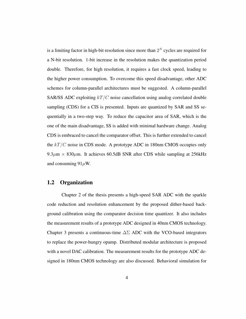
2.10 Architecture of the proposed SAR ADC. . . . . . . . . . . . . . . . 23
2.11 Waveform: (a) normal operation; (b) metastability in the 3rd comparison 24
2.12 Choice of the window width W (τ). . . . . . . . . . . . . . . . . . 26
2.13 Dither based background calibration of window width W . . . . . . . 27
2.14 Schematic of (a) comparator, (b) latch, and (c) tunable delay . . . . 30
2.15 Chip die photo. . . . . . . . . . . . . . . . . . . . . . . . . . . . . 31
2.16 Measured ADC output waveform with sparkle codes. . . . . . . . . 31
2.17 Measured sparkle code rate vs. sampling frequency . . . . . . . . . 32
2.18 Histogram of the location of the sparkle codes . . . . . . . . . . . . 33
2.19 Histogram of the magnitude of the sparkle codes . . . . . . . . . . 33
2.20 Histogram of MSB, 2nd MSB and 3rd MSB sparkle codes . . . . . 34
2.21 SNDR versus the probability of T = 1. . . . . . . . . . . . . . . . . 35
2.22 Measured ADC spectrum (213 points) . . . . . . . . . . . . . . . . 36
2.23 SNDR vs. input amplitude and frequency . . . . . . . . . . . . . . 37
2.24 DNL and INL plots . . . . . . . . . . . . . . . . . . . . . . . . . . 38
3.1 Architecture of the proposed VCO-based Σ∆ ADC. . . . . . . . . . 44
3.2 Individual block schematic. . . . . . . . . . . . . . . . . . . . . . . 45
xi

3.3 Layout of each slice and the ADC core. . . . . . . . . . . . . . . . 47
3.4 Measured DAC element selection pattern. . . . . . . . . . . . . . . 48
3.5 ADC die photo . . . . . . . . . . . . . . . . . . . . . . . . . . . . 50
3.6 Extracted DAC mismatch errors . . . . . . . . . . . . . . . . . . . 51
3.7 Measured ADC spectrum before and after calibration (218 points). . 52
3.8 Measured SNDR and SFDR vs. input amplitude at fV CO = 29.4MHz 52
3.9 (a) Existing VCO-based integrators. (b) Proposed implementation. . 57
3.10 Behaviors of (a) a standard quantizer and (b) a VCO phase quantizer. 59
3.11 (a) Proposed VCO-based integrator, and (b) its operation principle. . 60
3.12 (a) PWM behavior of VCO-based integrator, (b) equivalent circuit. 62
3.13 Quantization noise spectrum in (a) logarithmic and (b) linear scale. . 64
3.14 Simulated ADC output spectra. . . . . . . . . . . . . . . . . . . . . 65
4.1 Architecture of the proposed SAR/SS ADC. . . . . . . . . . . . . . 71
4.2 Alternative architecture of SAR/SS ADC. . . . . . . . . . . . . . . 72
4.3 (a) Timing diagram, (b) Behavior of VP . . . . . . . . . . . . . . . . 73
4.4 CLKS and CLKR in (a) a normal operation, (b) CDS. . . . . . . . . 75
4.5 Schemtaic of the continuous comparator . . . . . . . . . . . . . . . 76
4.6 (a) Schematic of the ramp generator, (b) VRAMP behavior . . . . . 77
4.7 (a) Die photo, (b) Layout of the SAR/SS ADC . . . . . . . . . . . . 79
4.8 Plots of (a) SAR, (b) single-slope, and (c) the reconstructed output . 80
4.9 Measured ADC spectrum (a) before, and (b) after calibration. . . . . 81
4.10 (a) Output after CDS, (b) Histogram of output . . . . . . . . . . . . 82
4.11 DNL and INL plots . . . . . . . . . . . . . . . . . . . . . . . . . . 83
xii

Chapter 1
Introduction
1.1 Motivation
The demand for higher power efficiency has been increasing in many appli-
cations such as sensors or wireless communication as portable devices or Internet
of Things (IoT) have been attracting lots of attention over the years. As an impor-
tant interface between the analog world and the digital implementation, analog-to-
digital converters (ADCs) also have been driven towards higher power efficiency.
To this end, many techniques have been developed by researchers for various ADC
architectures. Currently, pipeline, successive approximation register (SAR) and ∆Σ
ADCs are dominant ADC architectures. In the specific application such as CMOS
image sensors, single-slope (SS) ADCs are widely used.
In this thesis, advanced design techniques for a SAR ADC, a continuous-
time ∆Σ ADC, and a SS ADC are presented. They are implemented differently in
each ADC by (1) resolution enhancement while removing the sparkle code errors
in the SAR ADC, (2) replacement of the conventional power-hungry component
with voltage controlled oscillators (VCOs) along with the DAC calibration in the
continuous-time ∆Σ ADC, and (3) conversion speed increase and kT/C noise can-
cellation from two-step conversion by adopting SAR into the SS ADC.
1

SAR ADC is a popular choice due to its simple architecture and no need
of opamps. In addition, due to the digital-friendly design nature, its bandwidth
is increased as the technology scales, which broadens the application of SAR to
high-speed data communication systems for higher power efficiency. Another re-
quirement placed is the bit error rate (BER). Low BER is important for applications
such as instrumentation. Therefore, a technique for high-speed SAR ADCs having
low BER along with low power consumption is needed. This thesis presents a 6-b
high-speed SAR ADC with sparkle code correction. By quantizing the compara-
tor decision time (CDT), the sparkle codes are identified and corrected, reducing
the error rate from 10−4 to below 10−9. Furthermore, CDT quantization enables
1-bit increase in the ADC resolution by setting the detection boundary to be ±0.25
LSB. Thus, only 5 comparison cycles are needed to reach 6-b, leading to increased
ADC speed. The DAC also only needs to be 5-b, resulting in reduced chip area and
faster settling. A novel dither-based background calibration technique is devised
to accurately control the CDT detection window size and ensure PVT robustness.
A prototype ADC in 40nm CMOS achieves 35.3dB SNDR and consumes 0.81mW
while sampling at 700MS/s.
Continuous-time ∆Σ ADCs gain popularity in the wide bandwidth appli-
cation due to the following advantages. By taking advantage of the noise shaping
from the oversampling, inaccurate components can be used along with the inherent
anti-aliasing property, which makes the power-efficient design possible. However,
in the advanced nanometer-scale CMOS process, conventional ∆Σ ADCs employ-
ing the operational transconductance amplifiers (OTA) encounter difficulties due to
2

the smaller gain and reduced signal swing. An emerging and promising approach
to design ∆Σ ADCs is to use VCOs built with a ring of inverters. Ring VCOs act as
both integrators and quantizers in the phase domain. Thus, they can replace OTA-
based integrators and flash quantizers in conventional ∆Σ ADCs. Despite the many
merits, VCO-based ADCs have one major limitation, which is VCO’s nonlinear fre-
quency tuning characteristic. Thus, it is desirable to develop power-efficient way to
suppress the VCO’s nonlinearity while taking advantage of the merits. In this thesis,
a low-power and small-area VCO-based closed-loop ∆Σ ADC with two highlights
is presented. First, the ADC has a distributed modular architecture. It consists
of repetitive slices, which simplifies both schematic and layout design. It allows
the ADC to be easily reconfigured for other resolution specifications. Second, a
novel digital DAC mismatch calibration technique is proposed. It has low hardware
complexity by taking advantage of the intrinsic clocked averaging (CLA) capabil-
ity of dual VCO-based integrator. It ensures high linearity in the presence of large
DAC mismatches. A prototype ADC in 130nm CMOS occupies only 0.04mm2 .
It achieves 71dB SNDR over 1.7MHz BW while sampling at 250MS/s and con-
suming 0.9mW under a 1.2V supply. In addition, purely-VCO-based single-loop
second-order continuous-time ∆Σ ADC is presented with the behavioral simula-
tion. This exploits the pulse width modulation (PWM) property of the VCO-based
integrator to build up the second-order modulator.
A SS ADC is widely used in column-parallel architectures in a CMOS im-
age sensor (CIS). It offers good linearity and has a very simple architecture. It
mainly consists of a single comparator with small area. However, conversion time
3
is a limiting factor in high-bit resolution since more than 2N cycles are required for
a N-bit resolution. 1-bit increase in the resolution makes the quantization period
double. Therefore, for high resolution, it requires a fast clock speed, leading to
the higher power consumption. To overcome this speed disadvantage, other ADC
schemes for column-parallel architectures must be suggested. A column-parallel
SAR/SS ADC exploiting kT/C noise cancellation using analog correlated double
sampling (CDS) for a CIS is presented. Inputs are quantized by SAR and SS se-
quentially in a two-step way. To reduce the capacitor area of SAR, which is the
one of the main disadvantage, SS is added with minimal hardware change. Analog
CDS is embraced to cancel the comparator offset. This is further extended to cancel
the kT/C noise in CDS mode. A prototype ADC in 180nm CMOS occupies only
9.3µm × 830µm. It achieves 60.5dB SNR after CDS while sampling at 256kHz
and consuming 91µW.
1.2 Organization
Chapter 2 of the thesis presents a high-speed SAR ADC with the sparkle
code reduction and resolution enhancement by the proposed dither-based back-
ground calibration using the comparator decision time quantizer. It also includes
the measurement results of a prototype ADC designed in 40nm CMOS technology.
Chapter 3 presents a continuous-time ∆Σ ADC with the VCO-based integrators
to replace the power-hungry opamp. Distributed modular architecture is proposed
with a novel DAC calibration. The measurement results for the prototype ADC de-
signed in 180nm CMOS technology are also discussed. Behavioral simulation for
4

the second-order purely-VCO-based modulator is performed. Chapter 4 presents a
two-step SAR/SS ADC for CIS to shorten the conversion time in the high-bit reso-
lution. The measured results are also shown in Chapter 4. The conclusion is drawn
in Chapter 5.
5

Chapter 2
Sparkle Code Correction and Resolution
Enhancement in SAR
This chapter1 presents a 6-b high-speed SAR ADC with sparkle code cor-
rection. By quantizing the comparator decision time (CDT), the sparkle codes are
identified and corrected, reducing the error rate from 10−4 to below 10−9. Fur-
thermore, CDT quantization enables 1-bit increase in the ADC resolution by set-
ting the detection boundary to be ±0.25 LSB. Thus, only 5 comparison cycles are
needed to reach 6-b, leading to increased ADC speed. The DAC also only needs
to be 5-b, resulting in reduced chip area and faster settling. A novel dither-based
background calibration technique is devised to accurately control the CDT detec-
tion window size and ensure PVT robustness. A prototype ADC in 40nm CMOS
achieves 35.3dB SNDR and consumes 0.81mW while sampling at 700MS/s.
This chapter is organized as follows: an introduction is first presented. De-
sign of the asynchronous SAR is explained and the sparkle code errors are analyzed
next. The ADC design and the proposed technique are followed. Finally, the mea-
surement results are shown, followed by the conclusion.
1This chapter is an extended work of the publication: Yeonam Yoon and Nan Sun, “A 6-bit
0.81mW 700-MS/s SAR ADC with Sparkle-Code Correction, Resolution Enhancement, and Back-
ground Window Width Calibration”, IEEE CICC, accepted, 2017. I thank Dr. Nan Sun for his
valuable advice in designing and testing of the prototypes.
6

2.1 Introduction
The demand for the higher power efficiency in high-speed low-to-moderate
resolution applications such as wireless communication makes successive approx-
imation register (SAR) analog-to-digital converters (ADCs) a popular choice. Due
to the digital-friendly design nature, its bandwidth is increased as the technology
scales, which broadens the application of SAR to high-speed data communication
systems for higher power efficiency [Kull et al. [2014]]. Around 20 fJ per con-
version step with higher-than 1GS/s sampling speed has been achieved with an
effective number of bit (ENOB) below 11b [Chan et al. [2017a]; Lin et al. [2016]].
Another requirement placed is bit error rate (BER). Low BER is important for ap-
plications such as instrumentation. For example, WLAN and instrumentation re-
quires BER to be lower than 10−9 and 10−12, respectively [Guhados et al. [2012]].
Bit errors occur from the sparkle codes due to the metastability of the compara-
tor. Although the metastability does not degrade the ADC performance much in
terms of SNDR since its occurrence is rare, complicated error correction is needed
to meet the BER specification [Agazzi [2008]]. High-speed SAR ADC experiences
the metastability issue more since less time is allocated to the comparator deci-
sion. Due to the importance, metastability in pipelined ADCs or various types of
SAR ADCs was studied by researchers theoretically [Hashemi and Razavi [2014];
Waters et al. [2012]; Chan et al. [2017b]].
For a synchronous SAR ADC, metastability means the comparator cannot
fully resolve within one comparison cycle, causing wrong outputs. For an asyn-
chronous SAR ADC [Chen and Brodersen [2006]], when metastability happens,
7

comparison cycle is elongated compared with the easy comparison with the large
input. The entire ADC conversion may not finish within the allocated conversion
time. However, if the cycle is too elongated, the ADC fails to convert the input. In-
complete comparison before the clock resets the comparator incurs sparkle codes,
which results in non-differential comparator outputs [Chan et al. [2015]]. This hap-
pens because comparator does not have enough time to regenerate a valid difference
within one asynchronous clock cycle when inputs are small. Since unresolved com-
parator outputs result in the wrong, non-differential reference voltage selection in
capacitive DAC arrays, it can cause larger sparkle codes.
There are several ways to reduce the sparkle code rate. One method is
to simply allocate more time for the comparator using the skewed devices in or-
der to wait for the more regenerated outputs [Chen and Brodersen [2006]], but
this sacrifices the conversion speed. Another method is to reduce the compara-
tor regeneration time constant, but it has a technology limit and can greatly in-
crease power. To avoid large speed or power penalty, researchers recently devel-
oped techniques [Chan et al. [2015]; Keane et al. [2017]; Duan and Alon [2015]].
[Chan et al. [2015]] monitors the differential controls of the DACs by the logic
detector and checks whether they are deviated within the conversion cycle. If the
non-differential DAC controls are detected, outputs are eventually overridden by the
mapped codes. [Keane et al. [2017]] uses an unresolved decision detection scheme
with the programmable delay. If an unresolved decision is observed after the pre-
scribed delay, subsequent decisions are ignored. Another technique proposed in
[Duan and Alon [2015]] is based on comparator decision time (CDT) quantization.
8

When metastability happens, the CDT is long. Thus, metastability can be detected
by comparing the CDT with a reference delay using an array of 1-bit time-to-digital
converters (TDCs). By recording which comparison cycle is in metastability, the
correct ADC output can be reproduced, leading to greatly reduced sparkle code
rate. Nevertheless, a key limitation of [Duan and Alon [2015]] is that both the CDT
and the reference delay are sensitive to process, temperature, and voltage (PVT)
variations. Careful foreground hand tuning is used in [Duan and Alon [2015]] to
set an appropriate reference delay, but it is unsuitable for practical use and is unre-
liable in the presence of temperature drift.
This chapter presents a novel sparkle-code reduction technique for high-
speed SAR ADCs. It builds upon the basic idea of CDT quantization of [Duan and Alon
[2015]], but it ensures PVT robustness by devising a new background calibration
technique. Moreover, it makes use of CDT quantization to gain 1-bit increase in the
ADC resolution. It works by setting the reference delay τ to match the CDT when
the comparator sees a ±0.25-LSB input. Background calibration of τ is enabled by
injecting a 0.5-LSB pseudo-random dither to the SAR ADC. If τ is set correctly,
the probability of the comparator seeing an input within ±0.25 LSB during all SAR
conversion cycles is 50%, which is independent of the ADC input because of the
injected uncorrelated dither. Thus, by continuously monitoring the rate of TDC
outputs being 1, τ can be background tuned to the desired value. Furthermore, by
setting the CDT window to be ±0.25 LSB, the ADC resolution can be increased
by 1-bit by making use of the TDC output, which effectively performs a 0.5-LSB
quantization. This means that the proposed architecture can use a 5-bit SAR ADC
9

to obtain 6-bit. The reduction in the number of comparison cycles increases the
ADC speed. In addition, only a 5-bit DAC is needed, leading to a smaller area and
faster setting, which also boosts the ADC speed. It is noted that 1-bit resolution
increase by using the metastability detector is proposed in [Shikata et al. [2012]].
It also tried to reduce errors originated from the metastability along with the ad-
dition of extra resolution. However, its speed is slow and it is still vulnerable to
metastability of the detector, which is not adequate for the high-speed ADC.
A prototype ADC equipped with the proposed technique is built in 40nm.
The measured sparkle code error is reduced from 10−4 to below 10−9. The SNDR is
increased from 30.2dB to 35.3dB, which validates the 1-bit resolution enhancement.
It samples at 700MS/s and consumes 0.81mW, leading to a Walden figure-of-merit
(FoM) of 24fJ/conv-step.
2.2 Design of Asynchronous SAR ADC
In order to improve the speed of SAR ADCs, asynchronous clocking has be-
come a popular selection (see Fig. 2.1). In conventional synchronous SAR ADCs,
conversion speed is determined by the worst case comparison cycle, which consists
of the maximum DAC settling time and CDT. Maximum CDT comes from the min-
imum resolvable input. Maximum DAC settling time generally happens at MSB
or 2nd MSB according to the switching scheme. Asynchronous SAR addresses
the fixed allocated time to the comparator [Chen and Brodersen [2006]]. A ready
signal (Rdy) is generated when the comparison is complete, and it triggers the fol-
lowing comparison. CDT depends on the difference between the input and the ref-
10

LogicSAR
EN
2C4C8C16C
VREFP
VREFN
CLK
CLK
D4 ~ D0
NORIN
CLKb
VP
DP
Rdy
VOM
VOP
CLKS
V
Figure 2.1: Asynchronous SAR ADC.
erence. Since the input falls within ±1
2LSB at only one conversion cycle in SAR,
asynchronous clocking gives the benefit of the shorter total conversion time in com-
parison with the synchronous counterpart. However, DAC settling time is still the
same in [Chen and Brodersen [2006]] as adjustment of the cycle is only about the
CDT. Still, the worst case DAC settling time is taken into account to determine the
DAC settling time of all cycles. To solve this issue, self-timing technique is tried.
For example, [Kapusta et al. [2013]] uses a DAC timer circuit to indicate that DAC
settling is finished, which leads to the next comparison cycle in an asynchronous
way.
CDT is longest when the input difference is within±1
2LSB. The input of the
comparator diverges from the reference in the following DAC settling phase in SAR
algorithm. In this case, we don’t need to wait for the DAC to be settled accurately.
11

tconv tconv tconv
tcomp tDAC
Large input
- short tcomp
- long tDAC
Small input
- long tcomp
- short tDAC
VP
Time
VREF
tcomp tDAC
V
Figure 2.2: Complementary relation between tcomp and tDAC .
Accurate DAC settling is only required when the input converges to the reference.
Under this circumstance, the comparator generates output quickly since the input is
not close to the reference. This means that the DAC settling time required is related
with the CDT. Generally speaking, from MSB to LSB, the amount of time required
by the comparator increases due to the reduced input swing. In contrast, the amount
of time that DAC requires for its settling reduces from LSB to MSB. Thus, if we
set a fixed time window for comparison and DAC settling, this leads to the most
efficient way of using time.
This can be understood in such a way that the comparator can borrow the
12

-1 -0.5 0 0.5 1
Comparator input
0
2
4
6
8
10
12
Num
ber
of ti
me
cons
tant
sN
compN
DACN
tot
Figure 2.3: tcomp and worst-case tDAC .
time from the DAC settling if it needs more time to generate the output. Fig. 2.2
illustrates this complementary behavior of the CDT (tcomp) and DAC settling time
(tDAC). At the first conversion, the input of the comparator (VP ) is large, leading
to the short CDT. Subsequent DAC selection moves VP down toward the reference.
Since accurate DAC settling is required, long tDAC is needed. Next comparison
shows the opposite case. tcomp is long as VP is close to the reference. It is clear
that the DAC voltage is chosen in such a way that VP diverges from the reference.
Therefore, we don’t need VP to be settled for the next comparison. DAC settling
continues in the next comparison cycle. Thus, tDAC can be set short. It is noted
that the conversion time (tconv) for both conversion is the same. Fig. 2.3 shows
13

CLK
NOR
CLKb
VPRdy
VOM
VOP
EN
CLK
Rdy
VOP
VOM
- Large input - Small input
skewed
Figure 2.4: Skewed inverters.
the amount of time constant for comparison decision, worst-case DAC settling, and
sum of two, respectively in 6-bit SAR simulation with the comparator input range of
-1 and 1 and the reference of 0. Note that the amount shown for DAC settling is the
worst-case amount at that input. Worst-case DAC settling happens when the input
settles to the opposite side with the smallest amplitude. This plot clearly shows the
relationship between tcomp and worst-case tDAC . When tcomp is long, tDAC is short
and vice versa. Maximum tconv stays constant across the input range except of the
input of 0. Therefore, in order to minimize the time wasted during the conversion
cycle, the relationship can be applied to the SAR implementation. Also note that a
technique dealing with the long CDT (over 5 in this figure) should be required to
remove the extremely long tcomp due to the metastability at 0 input.
In order to build up this scheme, time of one conversion should not depend
on CDT. This can be implemented by making the comparator faster by employing
the skewed inverters (in Fig. 2.1) instead of making the comparator waiting for
resolved comparator outputs as in Fig. 2.4. In the beginning, comparator outputs
(VOP , VOM ) stay at the same reset low voltage. After comparison starts, outputs
14

start to resolve. VOP and VOM increase together until the regeneration phase. If
that increase is detected by NOR instead of waiting for the fully resolved outputs, it
forces the ADC to proceed to reset the comparator after the prescribed delay which
is defined by the clock generation loop. In Fig. 2.4, even with the small input,
Rdy goes down before VOP and VOM resolve to the differential values due to the
lowered threshold. With the oppositely-skewed inverters, Rdy is generated later
with a big dependence on the input as illustrated in the dashed line. As mentioned,
unsettled DAC does not affect the next comparison. Reset time is adjusted by the
comparison time since large input leads to the quick resolved outputs, resulting in
the steeper change of Rdy. In this simple implementation, tconv is not perfectly
constant. However, by using the skewed inverters, the dependence on the input can
be reduced. This means that within relatively constant cycle, tcomp and tDAC is
self-adjusted according to the input without any external logic or timer. However,
if CDT is too long due to the metastability as in Fig. 2.3, the ADC may fail to
create the correct DAC voltages since the comparator is reset after a certain time
regardless. Therefore, the way to detect the long CDT is needed to remove the
errors.
2.3 Sparkle Code Error
2.3.1 Cause of Sparkle Code Error
As the speed continues to increase, less time is available for the compara-
tor decision leading to the metastability. Since outputs regenerate exponentially
with time, if the input is very close to the reference, the comparator takes a much
15

LogicSAR
CLK
D4 ~ D0
NOR
VP
CC4 ~ CC0
D
CLK CLK
CCi D
CLKSDi
XM
XM
Figure 2.5: Asynchronous SAR ADC with dynamic logic gates
longer time for a valid logic output within the allowable comparison time. There-
fore, elongated CDT causes the ADC not to finish within the allocated conversion
time. This results in the non-differential outputs of the SAR logic and DAC ar-
rays. Fig. 2.5 shows the comparator with SAR logic and NOR. Dynamic NOR
is employed to make the clock generation loop faster because of the less stacked
transistors. Not like the static NOR, it raises the ready signal even before the out-
puts are fully resolved. SAR logic also utilizes the dynamic logic with precharging,
selection and latch functions. Note that a keeper transistor is placed at VXP node
to push the differential transition quicker in the dynamic logic pair. As mentioned,
with a small input, a comparator does not have enough time to regenerate results
16

3 3.2 3.4 3.6 3.8 4 4.2
0
0.5
1
Vo
lta
ge
(V)
CLKS, CLK, VP
, VM
3 3.2 3.4 3.6 3.8 4 4.2
0
0.5
1
Vo
lta
ge
(V)
VOP
, VOM
3 3.2 3.4 3.6 3.8 4 4.2
0
0.5
1
Vo
lta
ge
(V)
VXP1
, VXM1
3 3.2 3.4 3.6 3.8 4 4.2
Time (ns)
0
0.5
1
Vo
lta
ge
(V)
DP1
, DM1
VOP
VOM
VXP1
VXM1
DM1
DP1
VP
VM
Figure 2.6: Sim. of the metastabiltiy-induced error
before the corresponding comparison cycle (CC in Fig. 2.5) turns off the middle
transistor in the logic. This entails non-differential voltages at the node VXP and
VXM , consequently producing non-differential DAC control voltages. In the worst
case, DAC control voltages do not change after the conversion, which leaves the
input voltage the same. Then the same metastability issue is again encountered in
the next comparison.
Fig. 2.6 illustrates this type of error in the worst-case simulation with the
input same as the reference. Subscript 1 means the first cycle. As can be seen in
the plot, at the end of the first comparison cycle, comparator outputs VOP and VOM
cannot generate the valid logic outputs. Due to the dynamic NOR, even unresolved
17

outputs raise the ready signal, which reset the comparator. As a result, VXP1 and
VXM1 are not in the differential state. Owing to the keeper transistors, voltages keep
changing slowly. Note that DAC voltage VM1 increases even after the first cycle,
which causes the input of the comparator to change on. This contributes to the large
sparkle code errors. This concludes that schemes to avoid the metastability-induced
errors are required, especially in the high-speed SAR design with less available
comparison time.
2.3.2 Sparkle Code Removal Tachniques
Simple technique is to allocate more time to the comparator using the skewed
devices at the last inverter stage of the comparator to effectively make the CDT long
because the clock depends on CDT, therefore reset time is delayed. However, this
sacrifices the conversion speed even in normal condition. Simulation shows that
speed can be slower by 20% or more. Another way to use the latched output (DP
and DM in Fig. 2.5) instead of comparator outputs (VOP and VOM in Fig. 2.5)
for the inputs of NOR. This slows down clock generation. Since comparison cycle
(CC in Fig. 2.5) also depends on the clock cycle, more time is allowed for the com-
parison. Disadvantage is that time to go through the dynamic logic gate is wasted
regardless of the metastability. This concludes that detection of the metastability-
induced errors and replacement of outputs [Chan et al. [2015]; Keane et al. [2017]]
is better than the artificial CDT elongation. As mentioned earlier, CDT quantiza-
tion technique is proposed by [Duan and Alon [2015]]. Fig. 2.7 shows how CDT
quantization works. VOP and VOM are reset to high before comparison. After CLK
18

τ
CLK
CLK CLK
τ τ
rge inp all input
- Large input - Small input
Figure 2.7: CDT quantization
fires, a latch detects the output of NOR (Rdy) after τ delay. When the input dif-
ference between VP and VM is small, metastability happens. Therefore, the CDT
is long. Thus, ready goes down later than τ . In result, the latch catches high to
tell that the metastability happens. This process can be seen as comparison of CDT
with a reference delay using an array of 1-bit time-to-digital converters (TDCs). By
19

CLK
Rdy
CLKd
f
t
jr jr
tjr
CLK
f
t
tjr
μ μ
Figure 2.8: False negative detection error
recording which comparison cycle is in metastability, the correct ADC output can
be reproduced as in [Chan et al. [2015]].
2.3.3 Metastability Detection Error Analysis
There are two types of errors in the proposed metastability detection tech-
niques [Duan and Alon [2015]]. One is false positive error, which means that
metastability is detected by the detector, but actually the comparator is not in metasta-
bility. This error happens when the residue is very close to the detection window,
therefore, only to increase the noise. The other is false negative error, which is that
although hard metastability happens, it is not detected. This is primarily due to the
normally distributed instantaneous jitter of the tunable delay and the signal path.
20

Fig. 2.8 illustrates the jitter-induced detection errors. tjd represents an arrival time
of CLKd with a jitter of having a normal distribution with the mean of µCLKd and
the variance of σ2
CLKd. tjr is an arrival time of Rdy with a normally distributed
jitter with the mean of µRdy and the variance of σ2
Rdy. False negative error occurs
when CLKd comes later than Rdy due to the jitters as shown in Fig. 2.8(a). It also
happens when Rdy falls earlier than CLKd going up due to the jitters as illustrated
in Fig. 2.8(b). Since tjd and tjr are independent, the difference of tjd and tjr is also
a normal distribution with the mean of µ∆ = µCLKd − µRdy and the variance of
σ2∆= σ2
CLKd + σ2
Rdy. As the probability of Fig. 2.8(a), P (tjd > tjr), is equivalent
to P (tjd − tjr > 0), the probability of the false negative error can be calculated by
the Q-function (Eq. 2.1) of the difference of the two normal distributions.
Q(x) =1√2π
∫ ∞
x
exp(−u2
2)du (x =
µ∆
σ∆
)
=1
2[1− erf(
x√2)] (2.1)
where erf means the error function. For Fig. 2.8(b), similar calculation
can be performed by using P (tjr < tjd) = P (tjr − tjd < 0) with the mean of
µRdy − µCLKd. Fig. 2.9 shows the calculation of the false negative detection error
rate according to the µ∆ which is normalized to σ∆. Standard deviations of tjr and
tjd are 0.17τcomp and 0.20τcomp, respectively, which are obtained from the simula-
tion. τcomp is the comparator regeneration time. As mentioned, sparkle code occurs
when the compactor cannot regenerate the outputs with the small input within the
elongated comparison time before the comparator reset. In the proposed SAR ADC,
21

Figure 2.9: Calculation of false negative detection error rate
that elongation corresponds to the more than 9 ∼ 10 times σ∆, where the false neg-
ative error rate is very low as shown in the shaded area in Fig. 2.9.
2.4 Proposed ADC Design
2.4.1 Design of the 5-b Asynchronous SAR ADC Core
Fig. 2.10 shows the schematic of the single-ended version of the proposed
ADC. Its core is a 5-bit SAR with asynchronous clock generation [Chen and Brodersen
[2006]]. After sampling, EN turns high and starts the first comparison [Fig. 2.11(a)
shows the timing diagram]. NOR detects when the comparison finishes. After two
22
τ
DD
C
R���
R���
CLK
CLK
D4 0
4 0I�
CLKb
�
�
ferential
D� D�
CC4 0
CC4 0
D�
CLKS
Figure 2.10: Architecture of the proposed SAR ADC.
inverter delay, it triggers the comparator reset, and then, initiates the next com-
parison. The SAR logic counts the comparison cycle [CCi being 1 indicates the
(5 − i)-th comparison cycle] and records the comparator outputs (D4 ∼ D0) us-
ing dynamic logic circuits to increase speed and save power. The DAC switching
scheme of [Liu et al. [2010]] is adopted to reduce DAC switching power. By split-
ting capacitors in half, it effectively realizes Vcm-based switching but without the
need to connect capacitors to Vcm, which would require a large switch size.
2.4.2 CDT Quantization and Sparkle Code Removal
The CDT quantization block is shown in the dashed blue box of Fig. 2.10.
The dynamic latch works as a 1-bit TDC that compares the CDT with a reference
23

CLK
CLKd
2
nEN
CLKS
Rdy
CLK
CLKd
� �
EN
CLKS
Rdy
(a) (b)
ττ
Figure 2.11: Waveform: (a) normal operation; (b) metastability in the 3rd compari-
son
delay τ . The latch is triggered after every comparison. Its output is stored in an
array of DFFs (T4 ∼ T0) according to the comparison cycle CCi. This way, when
comparator metastability happens, we will not only detect it but also know when it
happens.
Fig. 2.11(b) shows an example timing diagram when the 3rd comparison
has a long CDT. In this case, the NOR output Rdy arrives later than the delayed
clock CLKd, leading to T2 = 1. However, the error can be corrected because we
know the comparator input is very close to zero during the 3rd comparison based on
T2 = 1, and thus, we can directly obtain the correct ADC output based on D4 and
D3. We do not even need to know D2 ∼ D0. In other words, when we see Ti = 1,
we can directly assign Di ∼ D0. Table 2.1 summarizes how the ADC output is
corrected for any comparison cycle with a long CDT. For T2 = 1, D4D3D2D1D0
is replaced by D4D3011.
24

Table 2.1: Mapping from the raw ADC output to the corrected output.
D4 D3 D2 D1 D0 TT4 = 1 0 1 1 1 1 1
T3 = 1 D4 0 1 1 1 1
T2 = 1 D4 D3 0 1 1 1
T1 = 1 D4 D3 D2 0 1 1
T0 = 1 D4 D3 D2 D1 0 1
2.4.3 Choice of τ and 1-bit Resolution Enhancement
The value of the reference delay τ needs to be set very carefully. Let us
define the value of the comparator input that produces an equal delay of τ as W ,
where W is inversely proportional to τ . The TDC can be considered as a window
detector. It detects comparator input that falls inside [−W,+W ]. When the com-
parator input is within ±W , the TDC output is 1, otherwise, the TDC output is 0.
W needs to be set properly. It cannot be larger than 1 LSB, as otherwise, even when
the comparator is in normal operation with an input greater than 1 LSB, it would be
identified as being in metastability, causing ADC resolution degradation. W also
cannot be too small, as otherwise, a long CDT may not be detected by the TDC,
leaving some sparkle codes uncorrected.
We choose the value of τ such that its corresponding W is 0.25 LSB. In
other words, if the comparator input is within ±0.25 LSB, its CDT is longer than
τ and the TDC output will be 1. Choosing W = 0.25 LSB ensures that all sparkle
codes due to metastability are identified. More importantly, it enables 1-bit increase
in the ADC resolution. Fig. 2.12 compares three cases of W . The black vertical
25
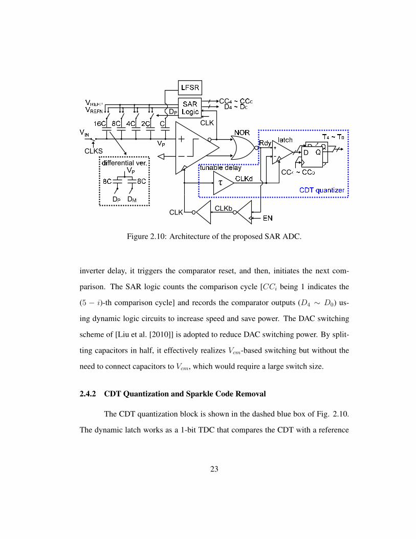
Figure 2.12: Choice of the window width W (τ).
line indicates the ADC input/output ranging from 0 LSB to 31 LSB for the 5-bit
SAR (k marks the location of k LSB). The red shaded part indicates the region over
which one TDC output Ti is 1. It is clear that if W = 0.25 LSB, the shaded and
unshaded regions evenly divide up the ADC input range. This indicates that one
extra bit can be obtained by making use of Ti. If we define T = T4||T3||T2||T1||T0
(T = 1 when any Ti is 1), then T provides a 0.5-LSB quantization and can be
directly concatenated with the corrected 5-bit ADC output D4D3D2D1D0 to obtain
a 6-bit ADC output, as D4D3D2D1D0T . This is also shown in Table 2.1. T is now
the new LSB of the 6-bit ADC: T = 1 when the input is in the red shaped regions,
and T = 0 otherwise.
26

inject 1/2 LSB dither
Figure 2.13: Dither based background calibration of window width W .
2.4.4 Background Calibration of the Reference Delay τ
Since the window width W is set by the delay τ , τ needs to be controlled
very accurately. Nevertheless, this is nontrivial because delay is sensitive to PVT
variations. Foreground calibration was used in [Duan and Alon [2015]] to manually
tune τ , but this is not suitable for practical application and cannot ensure robustness
when voltage or temperature drifts. Background calibration is necessary to ensure
PVT robustness.
We propose a novel background calibration technique that ensures W =
0.25 LSB. The key idea is based on monitoring the probability of T = 1. As shown
in Fig. 2.12, as W increases, the red shaded region enlarges, and thus, there is
a higher probability of T = 1 assuming a random input. Hence, by monitoring
P (T = 1) and adjusting τ to keep P (T = 1) = 50%, we can ensure that W =
27

0.25 LSB across PVT variation. The relation between P (T = 1) and resolution
improvement is as follows [Shikata et al. [2012]]. From this Eq. 2.2 (P (T = 1) is
abbreviated as P), if P (T = 1) = 50%, which means W = 0.25 LSB, then SNR
improvement is 6 dB.
∆SNR = −10× log(1− 3P + 3P 2) (P < 1) (2.2)
This background calibration scheme works well for a busy ADC input.
However, if the ADC input is a fixed DC value, the measured P (T = 1) be-
comes strongly input-dependent and no longer correlates well with W . For ex-
ample, if the DC input is right at the center of a red shaded region of Fig. 2.12(b),
P (T = 1) = 100% even though W = 0.25 LSB. This can cause τ to be incor-
rectly adjusted. To increase the robustness of the proposed background calibration
technique, we inject a 0.5-LSB pseudo-random dither into the SAR ADC after the
sampling phase as shown in Fig. 2.11. The dither is produced on-chip using a
linear feedback shift register (LFSR). The addition of the dither, together with the
inherent ADC noise, makes P (T = 1) independent from the ADC input. As shown
in Fig. 2.13, if an input falls into a T = 1 region, adding a dither pushes it into
a region with T = 0, and vice versa. This way, to the first order, P (T = 1) does
not depend on the input anymore; it depends only on the window width W . It is
noted that if there is no inherent noise, at certain DC, even with the window width
of Fig. 2.12(a) or (c), the P (T = 1) can be 50%. Inherent noise such as KT/C
helps to relieve this limitation. Simulation shows that noise with the sigma of 0.1
∼ 0.2 LSB is needed for this purpose. Thus, capacitive size and comparator are
28

designed to meet the above requirement. As a result, the proposed background cal-
ibration technique with dither can work for any type of ADC input regardless of its
amplitude, frequency, or distribution.
2.4.5 Circuit Implementation
The schematic of a comparator, a latch and a tunable delay used in the CDT
quantizer is shown in Fig. 2.14. A 3-stage comparator shown in Fig. 2.14(a) is
used for speed consideration, since it is two times faster than the 2-stage counter-
part. Double-tail comparator [Shinkel et al. [2007]] utilizes both CLK and CLKb
by placing PMOS instead of NMOS in the latching stage. This PMOS loads the
CLKb node of the asynchronous clock generation path. Inverters in the com-
parator are skewed to have the strong PMOS. Thus, once the conversion starts and
VP2/VM2 decrease in the beginning, OUTP /OUTM rise together up to the regener-
ation point. Since the dynamic NOR is used, the ready signal is raised even though
outputs are not fully differential. Furthermore, PMOS size is larger than NMOS for
the same strength, thus it further slows the asynchronous clocking.
Fig. 2.14(b) is the schematic of the latch in the CDT quantizer. As CLKd
and Rdy are both zero at sampling, a current tail transistor is removed for the fast
latching since less number of transistors are stacked without the tail NMOS tran-
sistor. Dynamic latch is placed prior to DFFs because DFF is slow to catch data
before the comparator is reseted. Tunable delay is shown in Fig. 2.14(c). Current-
controlled NMOS is inserted at the bottom of the first inverter. 3 inverters with the
appropriate size are followed. Delay can be tuned from 40ps to 100ps.
29

1st stage
VDD
CLK
CLK
CLK
CLK
VDD
�� VIM
V�VMV� VM
V�PVM2
V
V�PVM2OUT OUTM
CLKd CLKd
VDD
f
Rdy
CLKd CLKd
CLKd
VDD
CLK
VB
CLK CLKd
( ) t ab e de ay
para tch
2nd stage
3rd stage
Figure 2.14: Schematic of (a) comparator, (b) latch, and (c) tunable delay
2.5 Measurements
The prototype ADC in 40nm LP CMOS occupies 0.003mm2 (see Fig. 2.15
for die photo). The unit DAC capacitor is 0.25fF. Fig. 2.16 shows two example
measured ADC outputs with sparkle codes. With the proposed technique, these
sparkle codes are detected and corrected using Table 2.1.
30

49 m
62 m
LFSR
CDT quantizer
3SARlogic
ed switch
22
1
1
Figure 2.15: Chip die photo.
Figure 2.16: Measured ADC output waveform with sparkle codes.
Since ADC thermal noise can also cause small bit flips, we define the de-
tection of a sparkle code event only when the ADC error is greater than 4 LSB
31

200 300 400 500 600 700
fs
(MHz)
2
4
6
8
10
12
14S
pa
rkle
-co
de
ra
te (
%)
×10-5
Figure 2.17: Measured sparkle code rate vs. sampling frequency
(using the 6-bit scale). The measured sparkle-code occurrence is 1.9 × 10⁵ out of
2 × 10⁹ samples, leading to an error rate of 10−4. Sparkle code rate according to
the sampling frequency is measured and plotted in Fig. 2.17. Sparkle code rate
remains almost similar across the sampling frequency from 200MHz to 700MHz
under the same input frequency. This shows that major mechanism of the sparkle
code is the non-differential outputs of the comparator. If the elongated conversion
time is the cause, sparkle code rate should be in decrease as the sampling frequency
is reduced. With the proposed sparkle code reduction technique, we cannot mea-
sure any sparkle code, which indicates that the proposed technique has suppressed
the sparkle code rate to be below 5× 10⁻¹⁰.
Fig. 2.18 shows the histogram of the measured locations of the sparkle
32

Figure 2.18: Histogram of the location of the sparkle codes
-20 -15 -10 -5 0 5 10 15 20Sparkle-code error (LSB)
0
1
2
3
4
5
6
His
togr
am o
f spa
rkle
-cod
e er
ror
×104
Figure 2.19: Histogram of the magnitude of the sparkle codes
33

-20 -10 0 10 20
Sparkle-code error (LSB)
0
1
2
3
4
5
6H
isto
gra
m×104 MSB
-20 -10 0 10 20
Sparkle-code error (LSB)
0
1
2
3
4
5
6
His
tog
ram
×104 2nd MSB
-20 -10 0 10 20
Sparkle-code error (LSB)
0
1
2
3
4
5
6
His
tog
ram
×104 3rd MSB
Figure 2.20: Histogram of MSB, 2nd MSB and 3rd MSB sparkle codes
codes. As expected, since metastability can happen during any comparison cycle,
sparkle codes show up at all major MSB transitions. We have also measured the
magnitude of the sparkle code errors. Fig. 2.19 is the histogram of the measured
sparkle code error. The largest error is 17 LSB. The mean and standard devia-
tion are 8.2 and 3.9 LSB, respectively. Reason for the unequal distribution of the
above histograms are thought to be the unsymmetrical parasitic capacitance along
the differential paths. Fig. 2.20 shows three histograms corresponding to the first 3
MSBs. These plots show that most of the largest errors occur at MSB conversion.
The total number of sparkle code error is in increase from the 1st to the 3rd MSB as
expected. The reason why big sparkle code error occur is that combination of the
non-differential DAC voltages after the cycle and the slow change thereafter as can
34

Figure 2.21: SNDR versus the probability of T = 1.
be seen Fig. 2.6. This causes the input voltage of the comparator keep changing
after the corresponding cycle, which results in the wrong residue voltage.
The measured resolution improvement using the proposed technique versus
P (T = 1) is shown in Fig. 2.21. As expected, P (T = 1) = 50% leads to the
largest SNDR improvement. The green curve indicates the theoretical upper limit
for the resolution improvement from the equation 2.2. The measured result follows
it. There is a small 1-dB difference, which is due to ADC noise and capacitor
mismatch that are not considered in the theoretical calculation. The measurement
result of Fig. 2.21 also validates the proposed background calibration technique:
by adjusting the delay τ and keeping P (T = 1) = 50% in the background, we can
ensure robust operation across PVT variation. Since the estimation of P (T = 1)
35

1 2 3
×7
fIN
= 9.9 MHz
fS = 700 MHz (decimated by 8)
SNDR = 30.2 dB (w/o the proposed technique)
= 35.3 dB (w/ the proposed technique)
(dB
F
Figure 2.22: Measured ADC spectrum (213 points)
is fast, the convergence time of the proposed background calibration technique is
short. Measurement shows that 105 samples or 0.2ms is sufficient.
Fig. 2.22 shows the measured ADC spectrum. The sampling rate is 700MS/s
and the output is decimated by 8 to simplify testing. The measured SNDR of the
5-bit ADC core is 30.2 dB. It increases to 35.3 dB with the proposed resolution en-
hancement technique. The measured SNDR versus input amplitude and frequency
are shown in Fig. 2.23. Consistent SNDR improvement is obtained. Measured INL
and DNL are +0.9/−0.1 and +0.5/−0.4 LSB, respectively (in Fig. 2.24), limited
by capacitor mismatch.
The measured total ADC power is 0.81mW. The analog power consumed
36

Figure 2.23: SNDR vs. input amplitude and frequency
by comparator, asynchronous clock generation, and CDT quantizer is 0.4mW. The
reference power is 0.07mW. The digital power consumed by SAR logic and LFSR
is 0.34mW, Table 2.2 compares this work with other works. The measured Walden
FoM is 24.4 fJ/conv-step, which is in-line with the state-of-the-art.
2.6 Conclusion
This chapter presented a sparkle-code correction technique for high-speed
single-channel SAR ADCs. It can reduce the sparkle code error rate by more than 4
orders of magnitude. Moreover, it can increase 1-bit ADC resolution by setting
the metastability detection window to be 0.25 LSB. The robustness of the pro-
37

0 10 20 30 40 50 60
Output code
-1
-0.5
0
0.5
1
DN
L(LS
B)
0 10 20 30 40 50 60
Output code
-1
-0.5
0
0.5
1
INL(
LSB
)
Figure 2.24: DNL and INL plots
Table 2.2: Comparison with state-of-the-art 6b high-speed SAR ADCs
This workDuan and Alon
[2015]
Choo et al.
[2007]
Jiang et al.
[2012]
Feature
Sparkle-code reduction O O X X
1-bit resolution enhancement O X X X
Background calibration O X - -
Chip performance
Technology (nm) 40 LP 28 SOI 40 40
Type SAR TI SAR ciSAR SAR
Sample rate (GS/s) 0.7 0.64* 1 1.25
Bits 6 6 6 6
SNDR (dB) 35.3 25.2 34.6 31.8
ENOB 5.57 3.89 5.46 4.99
Power (mW) 0.81 5.3* 1.26 7.26
Area (mm2) 0.0031 0.14 0.00058 0.014
FOM (fJ/conv-step) 24.4 555 28.7 183
*single-channel performance
38

posed technique is ensured by a novel dither based background calibration tech-
nique based on probability measurement.
39

Chapter 3
VCO-Based Continuous-Time ∆Σ ADC
3.1 Modular Architecture and DAC Calibration
The first section1 of this chapter presents a low-power and small-area VCO-
based closed-loop ∆Σ ADC with two highlights. First, the ADC has a distributed
modular architecture. It consists of repetitive slices, which simplifies both schematic
and layout design. It allows the ADC to be easily reconfigured for other resolution
specifications. Second, a novel digital DAC mismatch calibration technique is pro-
posed. It has low hardware complexity by taking advantage of the intrinsic clocked
averaging (CLA) capability of dual VCO-based integrator. It ensures high linearity
in the presence of large DAC mismatches. A prototype ADC in 130nm CMOS oc-
cupies only 0.04mm2. It achieves 71dB SNDR over 1.7MHz BW while sampling
at 250MS/s and consuming 0.9mW under a 1.2V supply.
This section is organized as follows: an introduction is first presented. The
schematic and layout design of the proposed VCO-based ∆Σ ADC are explained
next. Explanation of the proposed digital DAC mismatch calibration technique is
1This section is a reprint of the publication: Yeonam Yoon, Kyoungtae Lee, Sungjin Hong,
Xiyuan Tang, Long Chen and Nan Sun, “A 0.04-mm2 Modular ∆Σ ADC with VCO-based Integra-
tor and 0.9-mW 71-dB SNDR Distributed Digital DAC Calibration”, IEEE CICC, pp. 1-4, 2015. I
thank all the co-authors for their valuable advice in designing and testing of the prototypes.
40

followed. Finally, the measurement results are shown, followed by the conclusion.
3.1.1 Introduction
Conventional ∆Σ ADCs rely on the use of operational transconductance
amplifiers (OTAs). However, they are scaling unfriendly, and consume large chip
area and power. They also require high gain (e.g., 60 dB) to ensure linearity and
accuracy; however, such high gain is hard to achieve in advanced CMOS process
with reduced transistor intrinsic gain. In addition, the reduced supply voltage makes
it hard to stack transistor vertically for gain boosting. A small supply voltage also
leads to reduced signal swing and dynamic range. The advent of nanometer tech-
nology calls for a new design methodology for ∆Σ ADC that not only does not
suffer from CMOS scaling but actually benefits from it.
An emerging and promising approach to design ∆Σ ADCs is to use volt-
age controlled oscillators (VCOs) built with a ring of inverters [Taylor and Galton
[2013]; Reddy et al. [2012]; Straayer and Perrot [2008]; Lee et al. [2013a]; Park and Perrot
[2009]; Rao et al. [2014]; Young et al. [2014]]. Ring VCOs act as both integrators
and quantizers in the phase domain. Thus, they can replace OTA-based integra-
tors and flash quantizers in conventional Σ∆ ADCs. VCO-based ADC are sim-
ple, low-power, small area, and operate well under low voltage supply. Moreover,
their performance naturally improves with CMOS scaling. The increased transistor
speed (fT ) and reduced inverter delay lead to higher VCO tuning gain and timing
resolution. The reduced transistor capacitance leads to lower VCO power.
Despite the many merits mentioned above, VCO-based ADCs have one ma-
41
jor limitation, which is VCO’s nonlinear frequency tuning characteristic. Several
techniques have been proposed to address this issue. Digital calibration can be used
for open-loop VCO-based ADCs [Taylor and Galton [2013]; Rao et al. [2014]]. This
method is mostly digital, but it depends on the accurate matching between the main
signal path and the replica path, which is hard to guarantee in the presence of PVT
variations. Another method is to embed the VCO in a feedback loop with an ana-
log filter preceding it [Straayer and Perrot [2008]]. This way, the VCO nonlinearity
is suppressed by the filter gain. However, this method still requires conventional
OTAs to build the filter, which is undesirable. In addition, this method uses VCO
only as a quantizer, and thus, the VCO input signal swing is still large, causing large
distortions. To reduce the VCO input swing, one approach is to perform residue
cancelation [Reddy et al. [2012]]. The other approach is to use VCO as an inte-
grator by outputting phase instead of frequency [Lee et al. [2013a]; Park and Perrot
[2009]; Young et al. [2014]]. To further reduce nonlinearity, dual VCO based inte-
grator can be used to suppress VCO’s dominant second-order distortion [Lee et al.
[2013a]].
This section presents a low-power and small-area closed-loop OTA-free ∆Σ
ADC. It uses ring VCO to perform both integration and quantization. There are two
key novelties for this work. First, the proposed ADC is mostly digital and highly
modular. It is comprised of an array of identical circuit slices. Each slice performs
a local integration, a 1-bit quantization, and a 1-bit current feedback. To our best
knowledge, our work is the first fully distributed ∆Σ ADC. Its topology is exactly
opposite to the conventional architecture whose integration, quantization, and feed-
42

back functions are lumped at separated circuit blocks. The repetitive and distributed
architecture of the proposed ADC greatly reduces the design complexity, and allows
it to be easily configured for different resolution specifications. To construct a m-
bit ∆Σ ADC, we can simply arrange (2m − 1) slices in a ring. The slice layout is
designed to be a rectangle with I/O on the two sides. Thus, when two slices are
placed nearby, they naturally connect to each other. Such arrangement significantly
reduces the layout effort.
One challenge for having a distributed architecture and layout is that the
DAC elements are no longer grouped together, but spread out over the entire ADC
area. The longer distance and less well matched surrounding environment causes
larger mismatches. Moreover, in order to embed a DAC inside a small slice layout
to reduce chip area and minimize wiring capacitance, the DAC area needs to be
small, which further increases mismatch. The second key novelty of this work is
that it proposes a novel DAC calibration technique that both digitally senses and re-
moves DAC mismatch errors. It has low hardware complexity by taking advantage
of the intrinsic clocked level averaging (CLA) capability of dual-VCO-based inte-
grator [Lee et al. [2013a]]. It ensures high linearity regardless of the VCO center
frequency.
A prototype ADC designed in 130nm occupies an area of only 0.04mm2. It
achieves 71dB SNDR over 1.7MHz BW while sampling at 250MS/s and consuming
only 0.9mW from a 1.2V power supply. The corresponding figure-of-merit (FOM)
is 98 fJ/conversion-step, which compares favorably to the state-of-the-art VCO-
based ∆Σ ADCs.
43

Figure 3.1: Architecture of the proposed VCO-based Σ∆ ADC.
3.1.2 Proposed ADC Architecture
Fig. 3.1 shows the proposed closed-loop ∆Σ ADC. The input resistor con-
verts the ADC input voltage to current. The subtraction between the input current
and the DAC feedback current happens at the VCO control nodes. The residue cur-
rent goes into the VCO and is integrated in the phase domain. To reduce power
consumption, no extra current is supplied for the VCO. In other words, the VCO
is solely powered up by the residue current. The ADC core consists of 31 identi-
cal slices. The VCO cell is a cross-coupled differential inverter [Fig. 3.2(a)]. The
buffer [Fig. 3.2(b)] isolates the VCO from the kickback noise from the comparator.
44

Figure 3.2: Individual block schematic.
It has the same structure as a VCO cell but with a smaller size. Due to the low swing
of the output of a VCO cell, a separate power supply (0.5V) is assigned to the buffer.
45

The comparator samples the VCO phase every clock period and the XOR gate per-
forms phase comparison. Note that although the two comparators and the XOR are
separately drawn in Fig. 3.1, they are merged into a single strong-arm latch with
an embedded XOR logic [Fig. 3.2(c)]. It saves power, reduces area, and shortens
the overall delay. The retiming latch [Fig. 3.2(d)] with half clock cycle delay is
added to remove input-dependent comparator delay. It embeds the make-before-
break scheme so as to minimize the glitch during DAC switching, which otherwise
produces distortion. The low swing DAC driver [Fig. 3.2(e)] is used to reduce the
coupling from the DAC control terminals to the output [Park and Perrot [2009]].
The cascode PMOS DAC is in Fig. 3.2(f). Thanks to the proposed digital DAC
calibration scheme which will be explained later, the DAC matching requirement is
significantly relaxed and a small DAC can be used.
The VCO nonlinearity issue is solved in the proposed ADC for the follow-
ing reasons: 1) the VCO acts as an integrator that provides gain, and thus, the
signal component at the VCO input is small; 2) the total DAC element is 31 (5-
bit), and thus, the quantization noise component at the VCO input is also small; 3)
the differential VCO structure cancels out the major VCO second-order distortion.
Measurement results confirm that the VCO-induced distortion is below −75 dBFS.
The distributed and modular structure of the proposed ADC greatly simpli-
fies the layout. As shown in Fig. 3.3(a), each repetitive slice is laid out as a rectan-
gular box. The entire ADC can be formed by simply aligning 31 slices on a track
[see Fig. 3.3(b) where numbers and arrows indicate direction]. This brings several
merits. First, the layout is very compact. The connected circuit blocks within each
46

Figure 3.3: Layout of each slice and the ADC core.
slice are placed very close to each other with shortest wires and minimum para-
sitics. It reduces chip area, shortens delay, and saves power. Second, the layout is
simple, digital like, and configurable. The input and output ports are located on the
same horizontal lines at the two sides of a slice. Thus, two slices can be automati-
cally connected when placed next to each other. The proposed layout design allows
quick change to the number of slices for different resolution specifications.
Global signals, such as clock, Vdd, Gnd, and VCO control nodes (VctrlN and
VctrlP ) are placed at the center of the ADC [Fig. 3.3(b)]. This provides matching
for the two sides. It also facilitates clock and power distribution by minimizing
horizontal distances. To improve matching accuracy, dummy slices are added at the
peripheral of the ADC core. Note that the empty space at the ADC center causes
slight VCO load mismatches between the slices at the center and those away from
47

Figure 3.4: Measured DAC element selection pattern.
the center, which results in a small phase non-uniformity. However, because the
phase error is high-pass shaped by the loop, its overall effect is negligible. Finally,
to reduce coupling, power domains are separated for sensitive circuits (VCO and
DAC) and non-critical blocks (comparator, XOR, and latch). Guard ring is also
added to provide further isolation.
3.1.3 Novel Digital DAC Calibration
Since small-area distributed DAC elements are used, they have large mis-
matches, which can severely degrade the ADC linearity. To address this issue, a
novel digital calibration technique with low hardware complexity is proposed. It
only adds a MUX before the DAC [Fig. 2.10]. The MUX can be merged with a
low-swing DAC driver [Fig. 3.2(f)]. When cal = 0, the driver output follows its
input. When cal = 1, the driver output is forced to 1.
48

During normal operation (cali = 0), the DAC selection follows the intrinsic
clocked averaging (CLA) behavior Lee et al. [2013a]. It is shown in Fig. 3.4(a)
where a solid box means its corresponding DAC element is on. The selection pattern
shifts every clock cycle at the rate of twice the VCO center frequency.
During calibration mode, both ADC inputs are shorted to Vcm. First, cal1
is set to 1. Thus, the first DAC element is always on regardless of the XOR output
[Fig. 3.4(b)]. Since the VCO is an ideal integrator with infinite gain in the phase
domain, the long-term average of the DAC output must equal to 31/2 = 15.5. Thus,
we have:
[1, p1,2, ..., p1,31]× [1 + e1, 1 + e2, ..., 1 + e31]T = 15.5 (3.1)
where {ei} represents DAC mismatch; {p1,i} denotes the probability of i-th DAC
element being on and can be measured by averaging the DAC input {di} over a
large number (e.g., 103) of samples. After {p1,i} are extracted, cal1 is reset to 0 and
cal2 is set to 1. We measure {p2,i} and have:
[p2,1, 1, ..., p2,31]× [1 + e1, 1 + e2, ..., 1 + e31]T = 15.5 (3.2)
The same process is repeated for all other DAC elements [see Fig. 3.4(c) for the
DAC selection pattern at i = 16]. Thus, a matrix of 31 equations can be formed:
1 p1,2 · · · p1,31p2,1 1 · · · p2,31
......
. . ....
p31,1 p31,2 · · · 1
1 + e11 + e2
...
1 + e31
=
15.515.5
...
15.5
(3.3)
Thus, we can solve {ei} by inverting (3.2). Once {ei} are obtained, DAC mismatch
errors can be easily removed from ADC output as in [Kauffman et al. [2014]]. The
49

Figure 3.5: ADC die photo
solving of {ei} is done off-chip in this design, but since it is purely digital, it can
be easily synthesized and integrated on chip. In addition, because we only need to
solve {ei} once per calibration, the required power is negligible.
3.1.4 Measurement Results
The prototype ADC occupies 0.04mm2 in 130nm CMOS [Fig. 3.5]. It
samples at 250MS/s and has a bandwidth of 1.7MHz at the OSR of 75. It consumes
0.9mW from a 1.2V supply.
The extracted DAC mismatch errors {ei} in percentage using the proposed
calibration technique is shown in Fig. 3.6. Because the DAC element is small
(12µm by 7µm) and distributed, their mismatches can be as large as 8%. The
50

0 5 10 15 20 25 30−0.1
−0.05
0
0.05
0.1
DAC element index
Mis
mat
ch {
e i }
Figure 3.6: Extracted DAC mismatch errors
standard deviation is 3.1%.
Fig. 3.7 shows the measured ADC spectrum at fin = 500kHz. The mea-
sured SNDR before calibration is 67.1dB. This performance is made possible by the
intrinsic CLA-based DEM that upshifts the majority of the DAC mismatch errors to
twice the VCO center frequency at 29.1MHz [Lee et al. [2013a]]. However, CLA
cannot completely remove the in-band mismatch error, which results in an increased
noise floor. After digital DAC calibration, the in-band mismatch noise is removed,
leading to an improved SNDR of 70.6dB. Measurement shows that 210 points are
sufficient for an accurate extraction of {ei}. Fig. 3.8 shows measured SNDR versus
input amplitude before and after calibration. The post-calibration dynamic range is
74dB.
51

Figure 3.7: Measured ADC spectrum before and after calibration (218 points).
−80 −70 −60 −50 −40 −30 −20 −10 0
0
10
20
30
40
50
60
70
Input amplitude (dBFS)
SN
DR
and
SF
DR
(dB
)
Before calibration
After calibration
Figure 3.8: Measured SNDR and SFDR vs. input amplitude at fV CO = 29.4MHz
52

The overall ADC performance is summarized in Table 1. Its Walden figure-
of-merit (FOM) is 98 fJ/conv-step, which compares favorably to the state-of-the-art
VCO-based ∆Σ ADCs, especially considering its relatively old 130nm process.
Because the proposed ADC is scaling friendly, its performance naturally improves
with CMOS scaling. Our simulation study shows that the same ADC design can
achieve an FOM of 20 fJ/conv-step if implemented in 65nm process.
Table 3.1: Comparison with other continuous-time ∆Σ ADCs
This
work
Taylor
[2013]
Rao
[2014]
Straayer
[2008]
Reddy
[2012]
Park
[2009]
Young
[2014]
Process [nm] 130 65 90 130 90 130 65
fs [MHz] 250 2400 640 950 600 900 1280
BW [MHz] 1.67 37.5 5 10 10 20 50
SNDR [dB] 70.6 70 73.9 72 78 78 64
Power [mW] 0.91 39 4.1 40 16 87 38
Area [mm2] 0.04 0.08 0.16 0.41 0.36 0.45 0.49
FOM [fJ/conv] 98 201 101 615 125 330 294
3.2 Purely-VCO-Based Second-Order ∆Σ ADC
The second section2 of this chapter reports a VCO-based single-loop continuous-
time (CT) ∆Σ analog-to- digital converter (ADC) that does not need any OTA-
based analog integrator. It achieves the second-order noise shaping by cascading
two VCO-based integrators and removing the sampling operation in the first VCO-
based integrator. Behavioral simulations confirm the validity of the proposed ADC
53

architecture.
This section is organized as follows: an introduction is first presented. The
proposed purely-VCO-based high-order ∆Σ ADC achritecture is discussed next.
Simulation results are shown, followed by the conclusion.
3.2.1 Introduction
CT Σ∆ ADCs have an advantage over discrete-time (DT) ones for low-
power applications. No settling behavior is involved, which otherwise requires
power-consuming operational transconductance amplifiers (OTAs) with high unity-
gain bandwidths in switched-capacitor circuits. It makes higher-frequency opera-
tion possible. CT ADCs also possess inherent anti-aliasing capability. In addition,
the input sampling is done after the loop filter. Thus, any sampling error is sup-
pressed by the loop filter along with the quantization noise [Yan and Sanches-Sinencio
[2004]]. One drawback for conventional CT ∆Σ ADCs is that they rely on the use
of OTA-based analog integrators that are power hungry and scaling unfriendly.
Recently, there have been emerging efforts to use ring VCOs to build CT
Σ∆ ADCs. VCOs can act as both integrators and quantizers in the phase do-
main, and thus, can replace OTA-based analog integrators and voltage comparators
used in conventional Σ∆ ADCs. The advantage for VCOs is that they are scal-
ing friendly, and thus, consume low area and power in advanced nanometer CMOS
2This section is a reprint of the publication: Yeonam Yoon, Kyoungtae Lee, and Nan Sun, “A
purely-VCO-based single-loop high-order continuous-time delta sigma ADC”, IEEE ISCAS, pp.
926-929, 2014. I thank all the co-authors for their valuable advice in designing and testing of the
prototypes.
54
processes. Moreover, the VCO resolution, set by the inverter delay, naturally im-
proves with CMOS scaling. So far, many first-order VCO-based ∆Σ ADCs have
been developed [Lee et al. [2013a]; Taylor and Galton [2010]; Lee et al. [2013b]].
Despite their design simplicity, they achieve only first-order shaping and require
a large over-sampling ratio (OSR) to guarantee a reasonable SNDR, leading to
a large sampling rate and clock power. Researchers have attempted to achieve
higher-order noise shaping by using the multi-stage noise shaping (MASH) struc-
ture [Hernandez [2012]; Yu et al. [2013]]; however, the loop mismatches cause
noise leakage and limit the ADC performance. Another method to achieve high-
order shaping is to place conventional OTA-based analog integrators in front of the
VCO [Straayer and Perrot [2008]; Park and Perrot [2009]]. Nevertheless, since the
first several integrator stages that dominate ADC power and noise still use OTAs,
the overall ADC performance enhancement brought by using a VCO-based last
stage is limited.
This section presents a single-loop second-order VCO-based CT Σ∆ ADC.
It is constructed by cascading two novel VCO-based integrators [Lee et al. [2013a,b]].
Note that the phase for any ring VCO is intrinsically quantized; in other words, any
VCO has an inherent built-in quantizer. Thus, we have to figure out a way to deal
with the quantization noise from the first VCO-based integrator, as its quantization
noise can only be first-order shaped. The proposed VCO-based integrator addresses
this problem by naturally performing a pulse width modulation (PWM) of its input,
and thus, the quantization error is moved out of the signal band. Moreover, un-
like the conventional VCO-based integrator that uses a reference sampling clock
55
[Park and Perrot [2009]], the proposed VCO-based integrator operates in a truly
CT fashion, which prevents the high-frequency quantization noise to be aliased
back into the signal band. As a result, the intrinsic quantization noise problem
in the first-stage integrator is solved, leading to the true second-order noise shap-
ing in a single-loop VCO-based ∆Σ ADC. Compared to prior arts, it does not
suffer from loop mismatches [Hernandez [2012]; Yu et al. [2013]] and completely
obviates the need for conventional analog integrators [Straayer and Perrot [2008];
Park and Perrot [2009]], thereby reducing power and area.
3.2.2 Second-Order Noise Shaping Using VCOs
Researchers have long desired a purely-VCO-based high-order CT ∆Σ ADC
architecture that obviates the need for analog integrators. However, it has not been
developed due to a number of difficulties. First, in order to use a VCO as an
integrator, its phase must be taken out as the output variable, instead of the fre-
quency (phase is proportional to integration of the VCO input, while frequency
is not). Most existing VCO-based ADCs can only output the digitized frequency
[Straayer and Perrot [2008]; Taylor and Galton [2010]]. They sample the outputs
of all VCO delay cells and compare them with the values sampled at the previous
clock cycle, so that the phase change, which is essentially the frequency, is ex-
tracted. However, if frequency is the output, the nice integration property of the
VCO is lost. Recently, researchers have developed a technique that can measure
the VCO phase [Park and Perrot [2009]]. It also samples the VCO delay cells, but
instead of comparing them with their previously sampled values, it compares them
56

-
+
VCO1
K/s
÷N
clk
DAC
VCO2
K/s
÷N
+
DAC
DA
C
Dout
V in
-
-
+
VCO1
K/s DAC
VCO2
K/s+
DAC
DA
C
V in
-
clkK/s0
K/s0
Dout
(a)
(b)
VCO3VCO4
Figure 3.9: (a) Existing VCO-based integrators. (b) Proposed implementation.
with a set of reference phases derived from the sampling clock [Park and Perrot
[2009]].
Based on this scheme, a natural extension to build a second-order CT ∆Σ
ADC would be to cascade two of these VCO-based integrators and wrap a feed-
back loop around them, as shown in Fig. 3.9(a). Nonetheless, this scheme does
not work for two reasons. First, because the output of the first VCO-based integra-
tor (VCO1) is sampled, the ADC does not operate in a truly CT manner. Second,
a VCO cannot produce an output phase with continuous amplitude; its phase is
inherently quantized. For example, an N-stage ring VCO can only produce 2N
discrete phases, which is different from a standard analog integrator whose output
57

voltage is continuous in amplitude. As a result, any VCO produces intrinsic quanti-
zation noise, and this noise is aliased into the signal band if sampled. Note that the
aliased quantization noise from VCO1 is only first-order shaped. Thus, even though
the quantization noise from VCO2 is shaped to the second order, the overall noise
shaping is only first order, as the in-band noise is dominated by that from VCO1.
To address these issues and achieve the second-order shaping, a novel VCO-
based ∆Σ ADC is proposed [see Fig. 3.9(b)]. In this architecture, the phase of
VCO1 is taken out by comparing its output stages with those from VCO3, which
is simply a copy of VCO1 but with a zero input. In real circuit implementation,
VCO3 is connected to the negative input Vinb, thus forming a differential setup.
Since the proposed comparison scheme operates in a CT way without sampling, a
true CT behavior is ensured. Furthermore, because no sampling is involved, there is
no aliasing of high frequency quantization noise from VCO1 and VCO3. However,
it does not remove any quantization noise, which can still dominate the overall in-
band quantization noise. Simulations show that if standard quantizers are used in
the model of Fig. 3.9(b), the overall noise shaping is only first order even though
the quantizer operates in a CT manner.
The most important feature to note is that the way a VCO phase quantizer
works is drastically different from that of a standard quantizer. This difference
brings a fundamental advantage to the VCO phase quantizer, which solves its quan-
tization noise problem. Fig. 3.10(a) shows the behavior of a standard voltage quan-
tizer with a ramp input. The output follows a staircase waveform; it does not change
unless the input crosses a quantizer threshold. Fig. 3.10(b) shows the input/output
58

Figure 3.10: Behaviors of (a) a standard quantizer and (b) a VCO phase quantizer.
characteristics for a VCO intrinsic phase quantizer. There is no clear threshold.
The output is constantly varying because the VCO phase keeps advancing with an
average rate of its center frequency. The result is that the VCO phase quantizer
essentially performs PWM of its input [Rao et al. [2011]]. This intrinsic phase
quantization property is exploited in the proposed VCO-based integrator.
The proposed VCO-based integrator is shown in Fig. 3.11(a). It consists of
59

Figure 3.11: (a) Proposed VCO-based integrator, and (b) its operation principle.
two identical VCOs, an array of N XOR gates and N 1-bit DACs. Here, the input
to VCO3 is connected to zero, but it can be connected to −x(t) in a differential
structure. Fig. 3.11(b) shows its operation principle. Here, θ is the phase of VCO3
which serves as a reference for VCO1, and v is the phase difference between VCO3
and VCO1. Note that since one entire VCO period means going around the ring
VCO twice, the corresponding phase range for the VCO loop shown in Fig. 3.11(b)
60
is from 0 to π, not 2π. The phase of VCO1 can be represented as
Φ(t) =
t∫
0
2π[KV COx(t) + fc]dt
= 2πKV CO
t∫
0
x(t)dt + 2πfct ≡ v + θ (3.4)
where KV CO is the VCO tuning gain and and fc is its free running frequency (center
frequency). θ increases at the speed of fc, and v varies according to the input. Since
the VCO has N stages, its phase quantization step is π/N . The phase difference is
detected using N XOR gates, which drive the 1-bit DAC array. As shown in Fig.
3.10, each DAC can be mapped to a phase on the VCO ring. Out of the N DACs,
the ones that are turned on (with corresponding XOR outputs being 1) are in the arc
of v.
Since all DACs operate in a similar way, it is sufficient to study the behavior
of only one DAC. For simplicity, let us examine the operation of the DAC at phase
0 (the shaded DAC in Fig. 3.11(b)). As explained earlier, it is selected only when
the arc of v contains it. Mathematically speaking, it means that the DAC input is 1
when:
θ + v > π → v > π − θ (3.5)
Here θ is wrapped into [0, π]. In other words, whenever it goes beyond π, we
subtract it by π.
Fig. 3.12(a) shows the equivalent operation of the VCO-based integrator
following the relationship of (3.5). Since θ increases from 0 to π, (π − θ) is drawn
61

Figure 3.12: (a) PWM behavior of VCO-based integrator, (b) equivalent circuit.
from π to 0. Dashed lines indicate the regions which satisfy the condition of (3.5).
As clearly seen, PWM signals are generated at the XOR output. This operation is
the same as that of the natural-sampling leading-edge PWM. It is well-known that
the ideal PWM operation does not produce distortions in the signal band, and the
tones are located around the PWM carrier frequency and its harmonics [Rao et al.
[2011]]. Here in our case, the PWM carrier frequency is 2 × fc, not fc, because 1
VCO period means going around the VCO ring twice (see Fig. 3.12).
62

Due to the aforementioned reasons, the amplitude information of the input
is not lost in the proposed VCO-based integrator, but is faithfully captured in the
output pulse width. Therefore, the VCO-based integrator produces a much more
accurate representation of the input than a standard quantizer. The effective in-
band (low frequency) quantizer resolution is much higher, and thus, the quantization
noise issue in the first VCO-based integrator is solved. From a frequency domain
perspective, although the total quantization noise power of the VCO phase integra-
tor is identical to that of a standard quantizer for the same quantization step, their
frequency domain distributions are significantly different. For the VCO-based in-
tegrator, due to its PWM behavior, its quantization noise in the signal band is very
small, and most of the noise is concentrated around the PWM carrier frequency
at 2fc. This high-frequency noise is sufficiently suppressed by the second-stage
integrator that works as a low-pass filter. As a result, the total amount of quantiza-
tion noise from the first stage VCO that shows up at the ADC output is negligible.
Consequently, almost ideal second-order noise shaping can be achieved with the
proposed architecture of Fig. 3.9(b), even though the first VCO-based integrator
produces quantization noise.
Fig. 3.13 shows 4,096 point FFT plots for a standard quantizer and a VCO-
based integrator. As clearly can be seen in Fig. 3.13(a), low-frequency quantization
noise of the VCO-based integrator is lower than that of the standard quantizer. In
Fig. 3.13(b), we can see concentrated noise around harmonics of PWM carrier
frequency. This quantization noise is shaped due to the feedback operation.
63

Figure 3.13: Quantization noise spectrum in (a) logarithmic and (b) linear scale.
3.2.3 Behavioral Simulations
To verify the proposed ADC architecture, behavioral-level simulations have
been performed in SIMULINK that conveniently provides built-in CT VCO mod-
els. The VCOs used in the ADC contain 15 delay cells each. The gains for VCOs
64

10-3
10-2
10-1-150
-100
-50
0
No
rma
lize
d a
mp
litu
de
[d
BF
S]
Scheme of Fig. 1(a)Proposed scheme of Fig. 1(b) withstandard integrators and quantizersProposed scheme of Fig. 1(b) withVCO-based integratorsIdeal 2nd-order noise shaping
40dB/dec
20dB/dec
Normalized frequency [f/f ]S
Figure 3.14: Simulated ADC output spectra.
and DACs are chosen in such a way that the noise transfer function for the second-
stage VCO quantization noise gives ideal second-order shaping (1 − z−1)2. Fig.
3.14 shows the simulation results for various configurations. As can be seen, the
∆Σ ADC that uses existing VCO-based integrators of Fig. 3.9(a) produces only
first-order noise shaping. The SQNR at the OSR of 30 is only 59 dB. The reason
is that the sampling operation in VCO1 aliases its quantization noise into the signal
band, which can only be shaped to the first order. Fig. 3.14 also shows that even if
the proposed ADC architecture of Fig. 3.9(b) is used but with standard quantizers,
the overall noise shaping remains only first order, because the quantization noise
from the first stage still dominates the in-band noise. Its SQNR of 64 dB is higher
65

than the prior case due to the removal of aliasing, but the improvement is limited.
By contrast, if the proposed architecture adopts the novel VCO-based integrators,
almost ideal second-order noise shaping obtained. The SQNR is substantially im-
proved to 81 dB. The intrinsic quantization noise problem of the first VCO-based
integrator is solved because the PWM behavior of the VCO phase quantizer en-
sures very low in-band quantization noise and moves the majority of the noise to
very high frequencies. These simulation results match well with the theoretical
analyses and firmly prove the feasibility of the proposed VCO-based high-order CT
∆Σ ADC architecture.
3.3 Conclusion
The first section presented a scaling friendly VCO-based ∆Σ ADC with
small area and low power. It has an interesting distributed and modular architecture,
which reduces design efforts and allows easy layout generation and reconfiguration
for different resolution requirements. Because the proposed ADC is highly digital
and regular, it also opens the door for both schematic and layout design automa-
tion. This work also proposed a novel digital DAC mismatch calibration technique,
which ensures a high linearity even in the presence of 8% DAC mismatch. It allows
the significant reduction of DAC area. This is critical for further ADC chip area
shrinking in advanced CMOS processes, as other ADC components are completely
digital, such as inverter, latch, and XOR.
The second section presented a purely-VCO-based single-loop second-order
CT ∆Σ ADC. It can be easily generalized to achieve even higher order noise shap-
66

ing. In the proposed VCO-based integrator, its intrinsic quantization noise is moved
out of band due to its inherent PWM property. A true CT operation also makes
sure that the high-frequency quantization noise is not aliased back to the signal
band. The proposed VCO-based ∆Σ ADC does not require any area/power con-
suming OTA-based analog integrator used in conventional ∆Σ ADCs. Because of
its scaling compatibility, it is envisioned that it can achieve superior performance in
advanced CMOS technologies.
67

Chapter 4
Twp-Step SAR/SS ADC
This chapter presents a column-parallel SAR/single-slope ADC exploiting
kT/C noise cancellation using analog correlated double sampling (CDS) for a
CMOS image sensor (CIS). Inputs are quantized by SAR and SS sequentially in
a two-step way. To reduce the capacitor area of SAR, which is one of the main
disadvantage, single-slope ADC is added with minimal hardware change. Analog
CDS is embraced to cancel the comparator offset. It is further extended to can-
cel the kT/C noise in CDS mode. A prototype ADC in 180nm CMOS occupies
only 9.3µm x 830µm. It achieves 60.5dB SNR after CDS with 256kHz sampling
frequency and 91µW power consumption.
This chapter is organized as follows: The schematic design of the proposed
SAR/SS ADC is first presented. The implementation of the circuit is explained
next. The measurement results are shown, followed by the conclusion.
4.1 Introduction
In CMOS image sensors, single-slope (SS) ADCs are widely used in column-
parallel architectures. It offers good linearity and has a simple architecture [Yoshihara et al.
[2006]]. It mainly consists of a single comparator with the small area. However,
68

conversion speed is a limiting factor in high-bit resolution since more than 2N cy-
cles are required for a N-bit resolution. 1-bit increase in the resolution makes the
quantization period double. Therefore, for high resolution, it requires a fast clock
speed, leading to the higher power consumption.
To overcome the speed disadvantage, other ADC schemes for column-parallel
architectures have been suggested to date. [Snoeij et al. [2007]] divides the input
range into m. It employs a coarse ramp and m multiple fine ramps in order to per-
form the two-step quantization. A fine ramp does not need to sweep through all
input range, but only 1
mspan after the coarse ramp determines the input subrange.
Although it shortens the conversion period, disadvantage of this work is the neces-
sity of m multiple ramps, which increases the power consumption and nonconfor-
mity between fine ramps. Cyclic ADC [M. Furuta and Kawahito [2007]] provides
fast operation speed. However, high-performance analog amplifier is required to
accomplish high gain and short settling time, which consumes considerable power.
∆Σ ADC is used in [Jo et al. [2016]], but it has the same disadvantage of using
the amplifier. Compared with the cyclic ADC, successive approximation regis-
ter (SAR) ADC [Matsuo et al. [2009]] removes the need for the amplifier, which
makes it the best power efficient scheme. It, however, requires accurate capacitor
matching especially in the high-bit application. Accordingly, its chip area becomes
very large, which is not appropriate for the column-parallel architecture. To solve
this issue, two-step approach combining SAR ADC and SS ADC is proposed in
[Tang et al. [2013]]. 3-bit SS conversion is first performed and then 8-bit SAR con-
version follows. Since 3 MSB bits are determined by SS, the total capacitance for
69

SAR can be reduced. Therefore, the area becomes smaller than 11-bit SAR ADC.
However, high and low reference voltages for SAR must be adjusted according to
the input subranges from the SS results. This means that many variable and accu-
rate voltage references must be required. Another disadvantage is that two separate
comparators are used for SS and SAR, which may cause the offset.
In this chapter, a two-step quantization ADC of 4-bit SAR + 8-bit SS topol-
ogy is presented. 4 MSB bits are determined by SAR ADC and the residue is
dealt with SS ADC. The proposed architecture incorporates SS ADC to SAR ADC
with no extra hardware cost except the ramp generator that is shared globally to all
column-parallel ADCs. One continuous comparator is used for both quantization
schemes with analog CDS technique. Since only 4 bits are converted by SAR, the
area of the capacitor array is smaller while taking advantage of the shorter conver-
sion time of SAR. Even though one cycle of SAR needs longer time than that of
SS, it still offers greatly reduced conversion time in comparison with the sole SS
ADC. In addition, CDS that is wildly adopted in ADCs for CIS are exploited to
reduce the thermal noise of the ADC. As the kT/C noise limits the resolution, the
capacitance must be big for high-bit resolution. Therefore, kT/C noise cancella-
tion helps to further relax the requirement of the total capacitor area. It is noted
that [Kim et al. [2016]] independently suggested the SAR/SS ADC. In our work,
analog CDS is used to implement the dual CDS. This helps to reduce the digital
measurement range of the offset in the pixel reset phase [Yoshihara et al. [2006]].
Another is to exploit the CDS to cancel the kT/C noise. With this technique, ca-
pacitor size can be smaller than the target resolution, resulting in the smaller area
70

Figure 4.1: Architecture of the proposed SAR/SS ADC.
and less power consumption.
A prototype ADC designed in 180nm occupies 9.7µm x 830µm. It achieves
56.3dB SNDR while sampling at 256kHz and consuming only 91µW. After CDS,
the remaining noise is measured to be 0.56LSB, which gives 60.5dB SNDR, 4dB
improvement.
4.2 Proposed ADC Architecture
Fig. 4.1 shows the proposed two-step SAR/SS ADC architecture employ-
ing 4-bit SAR and 8-bit SS quantization. Conventional binary-weighted capacitive
DAC array is used for 4-bit MSB SAR conversion. For SS, one unit capacitor (C)
is connected to a ramp generator block. A comparator is shared. Therefore, adding
SS to SAR does not require additional hardware. Separate clocks (CLKSAR and
CLKSS) are applied to each step. Input capacitor is for the analog CDS and noise
cancellation, which will be explained later. A multiplexer (MUX) is located prior to
the input capacitor. In the image sensor, there would be image pixels connected to
71

Figure 4.2: Alternative architecture of SAR/SS ADC.
the input capacitor. However, in this implementation, MUX is placed for sampling
instead of the image pixel since a photo diode was not offered in the process used.
Comparison voltage of the comparator is the same as VN , one of the MUX inputs.
It is noted that input is assumed to be above VN .
There can be an alternative architecture (Fig. 4.2). In this architecture,
there is no input attenuation. Fig. 4.1 suffers the input attenuation by 2 due to the
ratio of the input capacitance to the total DAC capacitance. However, Fig. 4.1 has
following advantages. Since the comparison voltage (VN ) is fixed, comparator does
not need large common mode rejection, which leads to simpler comparator design
with the low input swing . Furthermore, single-slope crossing voltage, VN , is also
signal independent. And linearity is not degraded by nonlinear capacitors at two
comparator inputs. However, owing to the signal attenuation, care must be taken
72

Figure 4.3: (a) Timing diagram, (b) Behavior of VP .
for the comparator design for the low input-referred noise.
Fig 4.3 describes a timing diagram of the ADC and behavior of the VP node
voltage. First, difference of VIN and VN is sampled on CLKS and ac-coupled to
73

VP node through an input capacitor with the attenuation by 2. At the same phase,
CLKR resets the SAR logic and the counter. During sampling, early CLKS
(CLKSe) turns on the switch to store the comparator offset at the input capaci-
tor for analog CDS. At the same time, this provides the DC bias to the VP node.
Since VP is in the middle of the capacitors, DC bias must be supplied. Feedback
around the first stage of the comparator works in a such way that VP becomes the
same as VN . Offset may exist, but it is canceled by the analog CDS. CLKSe goes
low slightly earlier than CLKS in the bottom-plate sampling way. After sampling,
charge stored at VP is converted by SAR and SS. Conventional DAC switching
technique is used. At the SAR phase, ramp signal is fixed to the certain DC, which
will be explained. As the input signal, reference voltage is also attenuated by 2. As
can be seen in the Fig. 4.3, each DAC reference voltage goes high first sequentially
and is chosen high until VP crosses VN . After 4 cycles, first 4 MSBs are deter-
mined. Then next quantization by SS begins. Since ramp only decreases, VP must
be larger than VN . Therefore, the ramp signal goes up to the full ramp voltage in
the first place, which requires some time for VP to settle. Same period of one SAR
cycle is allocated for settling. Ramp decreases while a counter block counts until
VP crosses VN . Due to the mismatches between capacitors, VP may not go over VN
at the start of SS phase. Thus, ramp range should be larger than LSB of SAR.
In CIS, CDS is adopted to cancel any offset of the readout path. It also can-
cels the reset noise of the image pixel. Owing to the consecutive conversion after
reset, the reset noise in two samples is correlated. This means that by subtracting
two samples, reset noise as well as offset can be canceled out. This can be extended
74

Figure 4.4: CLKS and CLKR in (a) a normal operation, (b) CDS.
to the cancellation of kT/C noise in the proposed architecture. After sampling,
kT/C noise is stored at VP node. Consecutive two conversions after sampling do
not change the kT/C noise. This means that kT/C noise sampled is correlated and
can be canceled by CDS. Therefore, kT/C noise can be larger than the design spec-
ification, which results in the relaxed requirement for the total capacitance, leading
to the smaller area. Furthermore, smaller capacitance makes the settling of the ref-
erence voltage in SAR faster. However, in the proposed scheme, the input signal
also gets canceled by CDS. The final resolution is estimated from the uncanceled
noise. The uncanceled noise is measured by converting the sampled input two times
and subtracting one from the other.
Timing for normal and CDS operation is shown in Fig. 4.4. In Fig. 4.4(a),
sampling is performed every time. In Fig. 4.4(b), input is sampled one time and then
converted two times. In this consecutive conversion, CLKR resets the SAR logic
and SS logic for ramp, which sets VP back to the point right after sampling (Fig.
4.3(b)). As mentioned previously, sampling noise is correlated to each conversion.
Therefore, remaining uncanceled noise after subtraction is less than the noise in a
75

Figure 4.5: Schemtaic of the continuous comparator
normal operation.
4.3 Circuit Implementation
Fig. 4.5 shows the continuous comparator design. It includes a differential
pre-amplifier followed by a single-ended common-source amplifier. Strong-arm
latch is avoided at the cost of the slower speed due to its dynamic behavior which
causes power noise crosstalk to the neighboring column-parallel ADCs. PMOS
input pair is chosen due to its superior flicker noise characteristic in comparison
with the NMOS input pair. The node VIN is connected to the VN in Fig. 4.1, and
the node VIP to the VP . During the sampling period, CLKSe is high to provide
76

Figure 4.6: (a) Schematic of the ramp generator, (b) VRAMP behavior
the bias to VP node since the node VP is ac-coupled to the input and SAR reference
voltages and is not connected directly to the DC bias. It also gives the benefit of
input offset cancellation by storing the comparator offset across the input capacitor
during sampling. M4 and M5 are inserted as abrupt change of VP during SAR
operation causes huge coupling to VOP node, which leads to the conversion error.
However, this induces higher gain and lower 3-dB bandwidth. Therefore, settling
time becomes longer.
A ramp generator for the single-slope ADC is represented in Fig. 4.6(a).
PMOS current sources (M1) and switches (M3) are used in a ramp generator.
Switches control the current through the resistor which sets the voltage at the output
node (VRAMP ). M2 is inserted to suppress the coupling from SW signals to VBP .
This interference can cause the fluctuation of VBP , causing the unwanted current
77
change. Since this output is shared through all column-parallel ADCs, resistance
must be low so as to have small RC constant. Currently 500 ohm is chosen. To
absorb the power and prevent kickback noise from the high swing input of SW
signals, a large capacitor is located between power supply and VBP and VBP2. SW
signals are generated by DFFs in the ramp logic block.
Redundancy of the ramp is illustrated in Fig. 4.6(b). Mismatch of the ca-
pacitors causes an offset that may be bigger than the desired magnitude of LSB of
SAR. This must be dealt with. Redundancy can be added to SAR or SS. However,
redundancy in SAR usually needs one more capacitor and cycle, which might not
be appropriate as it consumes area and waste conversion time. Because area restric-
tion is tough in this application, redundancy in single-slope is a better choice. Even
though this needs more current sources in a ramp generator, the ramp is shared to all
ADCs so area penalty is small. In this circuit, 94 more current sources are added to
256 current sources in both lower and upper direction. It operates as follows (Fig.
4.6(b)). Ramp voltage is set to the voltage of 47 × IRAMP during sampling/SAR
operation and jumps to 350 × IRAMP by turning on all current sources after first 4
SAR cycles. One more cycle is allocated for settling. Then ramp moves downward.
SAR logic is divided into two according to the global and local operation to
save the area. On each SAR cycle, a reference voltage is applied to each capacitor,
and the final DAC voltage is determined based on the comparison result. The former
is the same to all column-parallel ADCs, therefore this part can be a global block.
For the counter, ring counter is used since it requires only one clock. This leads to
the small power consumption and less clock routing complexity.
78

Figure 4.7: (a) Die photo, (b) Layout of the SAR/SS ADC
4.4 Measurement
The prototype ADC is fabricated in 180nm CMOS and occupies an area
of 9.3µm x 830µm as shown in Fig. 4.7. Fig 4.7(a) shows the chip die photo. It
consists of 50 ADCs in a column-parallel architecture and a ramp generator. Fig.
4.7(b) illustrates the layout of the single-channel SAR/SS ADC. Analog blocks
including a MUX, a comparator and input/DAC capacitors are 200µm long. The
comparator is placed between the input capacitor and DAC capacitors. MOM cap
is used and unit cap size is 10fF. Total capacitance is around 320fF. Latches and
buffers are needed for output selection among column-parallel ADCs. Analog and
digital power supplies are 2.8V and 1.8V, respectively. Input range is 1.25V and is
assumed to be over 1.0V (VN ). This is reasonable as the reset voltage of the pixel
is close to the power supply. In this measurement, SAR and SS clocks are 3.5MHz
and 175MHz, respectively, which gives 256kHz conversion speed.
Time domain outputs are plotted in Fig. 4.8. Fig 4.8(a) is the reconstructed
SAR output in the voltage domain. Output of the counter in the SS conversion is
shown in Fig. 4.8(b). 1 count number corresponds to the 1 step in ramp. Due to the
larger-than-expected parasitic capacitance between the comparator and the counter
(Fig. 4.7(b)), it takes many clock cycles for the comparator output to stop the
79

500 1000 1500 2000 2500Output sample
0
0.5
1V
olta
ge (
V)
SAR
500 1000 1500 2000 2500Output sample
200
250
300
350
Cou
nt
Single-slope
500 1000 1500 2000 2500Output sample
0
0.5
1
Vol
tage
(V
)
SAR-SS output
Figure 4.8: Plots of (a) SAR, (b) single-slope, and (c) the reconstructed output
counter. This is reflected in Fig. 4.8(b). As can be seen, count spans between 220
and 360. Since the ideal minimum number is around 50 as explained in the previous
section, high number of the minimum count means that transition of the comparator
output is slower than estimation due to the large parasitic capacitance. In order to
constrain the maximum count of the output within the range of the ramp, resolution
of SS was diminished by increasing the ramp step size. The difference is 140, not
80
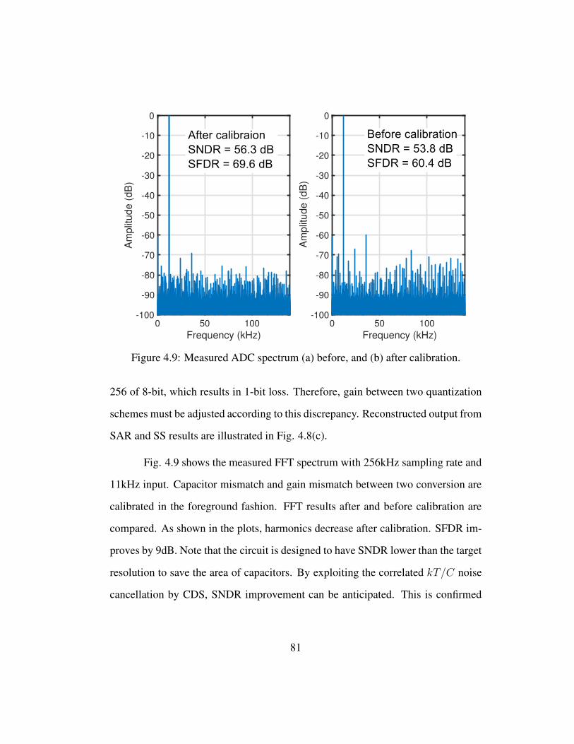
Figure 4.9: Measured ADC spectrum (a) before, and (b) after calibration.
256 of 8-bit, which results in 1-bit loss. Therefore, gain between two quantization
schemes must be adjusted according to this discrepancy. Reconstructed output from
SAR and SS results are illustrated in Fig. 4.8(c).
Fig. 4.9 shows the measured FFT spectrum with 256kHz sampling rate and
11kHz input. Capacitor mismatch and gain mismatch between two conversion are
calibrated in the foreground fashion. FFT results after and before calibration are
compared. As shown in the plots, harmonics decrease after calibration. SFDR im-
proves by 9dB. Note that the circuit is designed to have SNDR lower than the target
resolution to save the area of capacitors. By exploiting the correlated kT/C noise
cancellation by CDS, SNDR improvement can be anticipated. This is confirmed
81

500 1000 1500 2000 2500
Output sample
-6
-4
-2
0
2
4
6D
iffe
rence a
fter
CD
S (
LS
B)
-3 -2 -1 0 1 2 3
Difference (LSB)
0
0.1
0.2
0.3
0.4
0.5
0.6
0.7
0.8
PD
F
Histogram of difference
Normal distribution with σ = 0.58
Figure 4.10: (a) Output after CDS, (b) Histogram of output
by Fig. 4.10. Outputs are measured with DC input in order to convert the same
input multiple times. Fig. 4.10(a) shows the difference after CDS in LSB scale
with the DC input. Ideal plot is 0 along all output samples. From Fig. 4.10(b),
measured standard deviation is 0.56LSB, which is 440µVrms. This corresponds to
SNDR of 60.4dB with 1.3V input range. 3 4dB improvement is achieved. Effective
number of bits (ENOB) is estimated to be about 9.74-bit. Here, digital CDS is not
implemented. It is performed off-chip.
Measured DNL and INL are -0.96/1.44 LSB and -2.29/1.51 LSB respec-
tively in 10-bit scale. (Fig. 4.11). The total power consumption is 91µW, whose
breakdown is : 6µW used by analog blocks, 85 µW by digital blocks. Table 4.1
compares this work with other works.
82
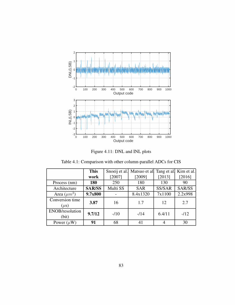
0 100 200 300 400 500 600 700 800 900 1000
Output code
-2
-1
0
1
2
DN
L(LS
B)
0 100 200 300 400 500 600 700 800 900 1000
Output code
-3
-2
-1
0
1
2
3
INL(
LSB
)
Figure 4.11: DNL and INL plots
Table 4.1: Comparison with other column-parallel ADCs for CIS
This
work
Snoeij et al.
[2007]
Matsuo et al.
[2009]
Tang et al.
[2013]
Kim et al.
[2016]
Process (nm) 180 250 180 130 90
Architecture SAR/SS Multi SS SAR SS/SAR SAR/SS
Area (µm2) 9.7x800 - 8.4x1320 7x1100 2.2x998
Conversion time
(µs)3.87 16 1.7 12 2.7
ENOB/resolution
(bit)9.7/12 -/10 -/14 6.4/11 -/12
Power (µW) 91 68 41 4 30
83
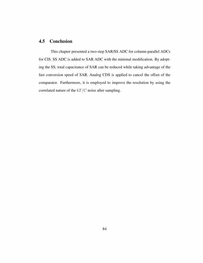
4.5 Conclusion
This chapter presented a two-step SAR/SS ADC for column-parallel ADCs
for CIS. SS ADC is added to SAR ADC with the minimal modification. By adopt-
ing the SS, total capacitance of SAR can be reduced while taking advantage of the
fast conversion speed of SAR. Analog CDS is applied to cancel the offset of the
comparator. Furthermore, it is employed to improve the resolution by using the
correlated nature of the kT/C noise after sampling.
84

Chapter 5
Conclusions and Future Directions
5.1 Conclusions
Advanced design techniques to address the current limitation are developed
for three types of ADCs : (1) high-speed SAR ADC, (2) continuous-time ∆Σ ADC,
(3) single-slope ADC for CMOS image sensors. Each prototype ADC was fabri-
cated and measured to validate the proposed techniques.
Chapter 2 presented a sparkle code reduction technique along with the res-
olution enhancement. Comparator decision time detector is inserted to monitor the
metastability event. Dither-based background calibration is proposed to adjust the
detection window to be half LSB, which leads to the 1-bit resolution enhancement.
This technique can reduce the total comparison cycles by 1. This cycle reduction
saves the power accordingly. Furthermore, comparator requirement to have a low
BER is relaxed by the proposed technique.
Chapter 3 presented a continuous-time ∆Σ ADC with VCO-based integra-
tors. It can replace the power-hungry op amp within the ∆Σ loop by converting the
data in the phase domain. On top of the inherent DEM property, which comes from
the dual-VCO-based architecture, a novel DAC calibration technique is applied to
relax the strict mismatch requirement on DACs in the feedback path. This makes
85

the small area of DACs possible to enable a compact layout. Distributed modu-
lar design, which is digital-friendly, is done utilizing the proposed technique. This
low-power benefit of VCO increases further as the technology scales. Chapter 3
also extends the work to the second-order single-loop purely-VCO-based ∆Σ ADC
in the behavior simulation. PWM property of the VCO-based integrator is analyzed
and used.
Chapter 4 showed the two-step ADCs by incorporating SAR into SS ADC.
The proposed two-step ADC shortens the conversion speed. In the proposed ar-
chitecture, kT/C noise cancellation through the analog correlated-double sampling
relieves the limitation of DAC area of SAR ADC.
5.2 Future Directions
The proposed dither-based sparkle code reduction technique can be applied
to the high-speed SAR ADCs. To this end, comparator and dynamic SAR logic
gates must be designed well in deeply scaled CMOS process since the current speed
limitation comes from the both. In addition, in order to use the complementary be-
havior of the comparator decision time and DAC settling time fully, synchronous
clocking can be applied instead of the asynchronous scheme. Although power con-
sumption of the clock network becomes more, it can operate faster due to the re-
duced loading of the NOR gate. Furthermore, conversion can be stopped after the
metastability detection to further decrease the power. However, in a high speed
SAR ADC, it is not easy to stop the conversion right after metastability occurrence
owing to the time needed to check the detection results and to stop the clocking
86

loop.
For the∆Σ ADC, with the proposed distributed modular architecture, continuous-
time ∆Σ ADC can be easily reconfigured based on the resolution requirement.
Also, layout can be automated if the slice is set as a basic building block. Due
to the proposed DAC calibration which solves the DAC nonlinearity, the size of the
slice having DAC inside can be smaller in the advanced CMOS process.
Two-step SAR/SS ADC can be more optimized to have the best perfor-
mance considering the trade-off between SAR and SS ADCs. kT/C noise can-
cellation is more actively exploited to further decrease the DAC capacitance. Since
input and DAC capacitors take huge area and put the stringent area limitation on the
layout, reduced DAC capacitance as well as input capacitance makes the SAR/SS
ADC smaller. However, since the capacitors should have higher-than the 12b ac-
curacy, unit capacitor size and layout should be considered well to reduce the ca-
pacitor mismatch. Clocked comparator is also used to make it faster. Continuous
comparator that is currently employed takes a longer time to resolve the output
while the counter keeps counting. Thus, by using the clocked comparator, out-
put resolving time can be shorter. However, in this case, power fluctuation may be
worse. Therefore, shielding between the neighboring column-parallel ADCs should
be done carefully.
87

Appendix
88

Appendix 1
List of Publications
1. Yeonam Yoon, and Nan Sun, “A 6-bit 0.81mW 700-MS/s SAR ADC with
Sparkle-Code Correction, Resolution Enhancement, and Background Win-
dow Width Calibration,” accepted to IEEE Custom Integrated Circuits Con-
ference (CICC), 2017.
2. Long Chen, Xiyuan Tang, Arindam Sanyal, Yeonam Yoon, Jie Cong, and
Nan Sun, “A 0.7V 0.6W 100kS/s Low-Power SAR ADC with Statistical Es-
timation Based Noise Reduction,” accepted to IEEE Journal of Solid-State
Circuits 2017.
3. Miguel Gandara, Wenjuan Guo, Xiyuan Tang, Long Chen, Yeonam Yoon,
and Nan Sun, “A Pipelined SAR ADC Reusing the Comparator as Residue
Amplifier,” accepted to IEEE Custom Integrated Circuits Conference (CICC),
2017.
4. Kyoungtae Lee, Yeonam Yoon, and Nan Sun, “A scaling-friendly low-power
small-area delta-sigma ADC with VCO-based integrator and intrinsic mis-
match shaping capability,” IEEE Journal of Emerging and Selected Topics in
Circuits and Systems, vol. 5, no. 4, pp. 561-573, Dec. 2015.
5. Yeonam Yoon, Koungtae Lee, Sungjin Hong, Xiyuan Tang, Long Chen, and
Nan Sun, “A 0.04-mm2 Modular ∆Σ ADC with VCO-based Integrator and
0.9-mW 71-dB SNDR Distributed Digital DAC Calibration,” Custom Inte-
grated Circuit Conference (CICC), pp. 1-4, Sep. 2015.
6. Long Chen, Xiyuan Tang, Arindam Sanyal, Yeonam Yoon, Jie Cong, and
Nan Sun, “A 10.5-b ENOB 645nW 100kS/s SAR ADC with Statistical Esti-
mation Based Noise Reduction,” IEEE Custom Integrated Circuit Conference
(CICC), pp. 1-4, Sep. 2015.
89

7. Yeonam Yoon, Kyoungtae Lee, and Nan Sun, “A purely-VCO-based single-
loop high-order continuous-time delta sigma ADC,” IEEE International Sym-
posium on Circuits and Systems (ISCAS), pp. 926-929, 2014.
8. Kyoungtae Lee, Yeonam Yoon, and Nan Sun, “A 1.8mW 2MHz-BW 66.5dB-
SNDR delta-sigma ADC using VCO-based integrators with intrinsic CLA,”
IEEE Custom Integrated Circuits Conference (CICC), pp. 1-4, 2013
9. Kyoungtae Lee, Yeonam Yoon, and Nan Sun, “A 10MHz-BW, 5.6mW, 70dB
SNDR ∆Σ ADC using VCO-based integrators with intrinsic DEM,” IEEE
International Symposium on Circuits and Systems (ISCAS), pp. 2006 2009,
2013.
Future publications
1. Yeonam Yoon, and Nan Sun, “A 6-bit 0.81mW 700-MS/s SAR ADC with
Sparkle-Code Correction, Resolution Enhancement, and Background Win-
dow Width Calibration,” to be submitted to IEEE Journal of Solid-State Cir-
cuits (JSSC).
2. Yeonam Yoon, and Nan Sun, “SAR/Single-Slope Two-Step Quantization for
CMOS Image Sensor Exploiting KT/C Noise Cancellation by Correlated
Double Sampling,” to be submitted to IEEE Transactions on Circuits and
Systems II: Express Briefs (TCAS-II).
90

Bibliography
L. Kull, T. Toifl, M. Schmatz, P. A. Francese, C. Menolfi, M. Braendli, M. Kossel,
T. Morf, T. M. Andersen, and Y. Leblebici. A 90GS/s 8b 667mW 64x interleaved
SAR ADC in 32nm digital SOI CMOS. In 2014 IEEE International Solid-State
Circuits Conference Digest of Technical Papers (ISSCC), pages 378–379, 2014.
C. H. Chan, Y. Zhu, I. M. Ho, W. H. Zhang, S. P. U, and R. P. Martins. A 5mW 7b
2.4GS/s 1-then-2b/cycle SAR ADC with background offset calibration. In 2017
IEEE International Solid-State Circuits Conference Digest of Technical Papers
(ISSCC), pages 282–283, 2017a.
Y. Z. Lin, C. H. Tsai, S. C. Tsou, and C. H. Lu. A 8.2-mW 10-b 1.6-GS/s 4x TI
SAR ADC with fast reference charge neutralization and background timing-skew
calibration in 16-nm CMOS. pages 1–2, 2016.
S. Guhados, P. J. Hurst, and S. H. Lewis. A pipelined ADC with metastability
error rate < 10−15 errors/sample. IEEE Journal of Solid-State Circuits, 47(9):
2119–2128, 2012.
O. E. Agazzi. A 90 nm CMOS DSP MLSD transceiver with integrated AFE for
electronic dispersion compensation of multi-mode optical fibers at 10 Gb/s. IEEE
Journal of Solid-State Circuits, 43(12):2939–2957, 2008.
S. Hashemi and B. Razavi. Analysis of Metastability in Pipelined ADCs. IEEE
Journal of Solid-State Circuits, 49(5):1198–1209, 2014.
A. Waters, J. Muhlestein, and U. Moon. Analysis of metastability errors in conven-
tional, LSB-fisrt, and asynchronous SAR ADCs. IEEE Transactions on Circuits
and Systems-I: Regular Papers, 47(4):1022–1030, 2012.
C. H. Chan, Y. Zhu, S. W. Sin, B. Murmann, S. P. U, and R. P. Martins. Metastablil-
ity in SAR ADCs. IEEE Transactions on Circuits and Systems-II: Express Briefs,
64(2):111–115, 2017b.
91
S. W. Chen and R. Brodersen. A 6b 600MS/s 5.3mW asynchronous ADC in 0.13µm
CMOS. In 2006 IEEE International Solid-State Circuits Conference Digest of
Technical Papers (ISSCC), pages 2350–2359, 2006.
C. Chan, Y. Zhu, S. Sin, S. U, and R. P. Martins. A 5.5mW 6b 5GS/s 4x-interleaved
3b/cycle SAR ADC in 65 nm CMOS. In 2015 IEEE International Solid-State
Circuits Conference Digest of Technical Papers (ISSCC), pages 466–468, 2015.
J. P. Keane, N. J. Guilar, D. Stepanovic, B. Wuppermann, C. Wu, C. W. Tsang,
R. Neff, and K. Nishimura. An 8GS/s time-interleaved SAR ADC with un-
resolved decision detection achieving -58dBFS noise and 4GHz bandwidth in
28nm CMOS. In 2017 IEEE International Solid-State Circuits Conference Di-
gest of Technical Papers (ISSCC), pages 284–286, 2017.
Y. Duan and E. Alon. A 6b 46GS/s ADC with >23GHz BW and sparkle-code
error correction. In 2015 Symposium on VLSI Circuits (VLSI Circuits), pages
C162–C163, 2015.
A. Shikata, R. Sekimoto, T. Kuroda, and H. Ishikuro. A 0.5V 1.1 MS/sec 6.3
fJ/conversion-step SAR-ADC with tri-level comparator in 40 nm CMOS. IEEE
Journal of Solid-State Circuits, 47(4):1022–1030, 2012.
R. Kapusta, J. Shen, S. Decker, H. Li, E. Ibaragi, and H. Zhu. A 14b 80 MS/s
SAR ADC With 73.6 dB SNDR in 65 nm CMOS. IEEE Journal of Solid-State
Circuits, 48(12):3059–3066, 2013.
C. Liu, S. Chang, G. Huang, Y. Lin, and C. Huang. A 1V 11fJ/conversion-step
10bit 10MS/s asynchronous SAR ADC in 0.18µm CMOS. In 2010 Symposium
on VLSI Circuits (VLSI Circuits), pages 241–242, 2010.
D. Shinkel, E. Menshink, E. Klumperink, E. van Tuijl, and B. Nauta. A double-tail
latch-type voltage sense amplifier with 18ps setup+hold time. In 2007 IEEE In-
ternational Solid-State Circuits Conference Digest of Technical Papers (ISSCC),
pages 314–315, 2007.
K. Choo, J. Bell, and M. Flynn. Area-efficient 1GS/s 6b SAR ADC with charge-
injection-cell-based DAC. In 2016 IEEE International Solid-State Circuits Con-
ference Digest of Technical Papers (ISSCC), pages 460–462, 2007.
92

T. Jiang, W. Liu, F. Y. Zhong, C. Zhong, K. Hu, and P. Y. Chiang. A single-channel,
1.25-GS/s, 6-bit, 6.08-mW asynchronous successive-approximation ADC with
improved feedback delay in 40-nm CMOS. IEEE Journal of Solid-State Circuits,
47(10):2444–2453, 2012.
G. Taylor and I. Galton. A reconfigurable mostly-digital Σ∆ ADC with a worst-
case FOM of 160dB. IEEE Journal of Solid-State Circuits, 48(4):983–995, 2013.
K. Reddy, S. Rao, R. Inti, B. Young, A. Elshazly, M. Talegaonkar, and P.K. Hanu-
molu. 16-mW 78-dB SNDR 10-MHz BW CT ADC using residue-cancelling
VCO-based quantizer. IEEE Journal of Solid-State Circuits, 47(12):2916–2927,
2012.
M. Z. Straayer and M. H. Perrot. A 12-bit 10-MHz bandwidth, continuous-timeΣ∆
ADC with a 5-Bit 950-MS/s VCO-based quantizer. IEEE Journal of Solid-State
Circuits, 43(4):805–814, 2008.
K. Lee, Y. Yoon, and N. Sun. A 1.8mW, 2MHz-BW 66.5dB-SNDR delta-sigma
ADC using VCO-based integrators with intrinsic CLA. In 2013 IEEE Custom
Integrated Circuits Conference (CICC), pages 1–4, 2013a.
M. Park and M. H. Perrot. A 78 dB SNDR 87 mW 20 MHz bandwidth continuous-
time Σ∆ ADC with VCO-based integrator and quantizer implemented in 0.13
µm CMOS. IEEE Journal of Solid-State Circuits, 44(12):3344–3358, 2009.
S. Rao, K. Reddy, B. Young, and P.K. Hanumolu. A deterministic digital back-
ground calibration technique for VCO-based ADCs. IEEE Journal of Solid-State
Circuits, 49(4):950–960, 2014.
B. Young, K. Reddy, S. Rao, A. Elshazly, T. Anand, and P. K. Hanumolu. A 75dB
DR 50MHz BW 3rd order CT-∆Σ modulator using VCO-based integrators. In
2014 Symposium on LSI Circuits (VLSI Circuits), pages 1–2, 2014.
J. G. Kauffman, P. Witte, M. Lehmann, J. Becker, Y. Manoli, and M. Ortmanns. A
72dB DR, CT Σ∆ modulator using digitally estimated auxiliary DAC lineariza-
tion achieving 88fJ/conv-step in a 25 MHz BW. IEEE Journal of Solid-State
Circuits, 49(2):392–404, 2014.
93
S. Yan and E. Sanches-Sinencio. A continuous-time Σ∆ modulator with 88-dB
dynamic range and 1.1-MHz signal bandwidth. IEEE Journal of Solid-State Cir-
cuits, 39(1):75–86, 2004.
G. Taylor and I. Galton. A mostly-digital variable-rate continuous-time delta-sigma
modulator ADC. IEEE Journal of Solid-State Circuits, 45(12):2634–2646, 2010.
K. Lee, Y. Yoon, and N. Sun. A 10MHz-BW, 5.6mW, 70dB SNDR Σ∆ ADC
using VCO-based integrators with intrinsic DEM. In 2013 IEEE International
Symposium on Circuits and Systems (ISCAS), pages 2006–2009, 2013b.
L. Hernandez. VCO based multi-stage noise shaping ADC. Electronics Letters, 48
(4):206–208, 2012.
W. Yu, J. Kim, K. Kim, and S. Cho. A time-domain high-order MASH Σ∆ ADC
using voltage-controlled gated-ring oscillator. IEEE Transactions on Circuits
and Systems-I: Regular Papers, 60(4):856–866, 2013.
S. Rao, B. Young, A. Elshazly, W. Yin, N. Sasidhar, and P.K. Hanumolu. A 71dB
SFDR open loop VCO-based ADC using 2-level PWM modulation. In 2011
Symposium on VLSI Circuits (VLSI Circuits), pages 270–271, 2011.
S. Yoshihara, Y. Nitta, M. Kikuchi, K. Koseki, Y. Ito, Y. Inada, S. Kuramochi,
H. Wakabayashi, M. Okano, H. Kuriyama, J. Inutsuka, A. Tajima, T. Nakajima,
Y. Kudoh, F. Koga, Y. Kasagi, S. Watanabe, and T. Nomoto. A 1/1.18-inch 6.4
MPixel 60 frames/s CMOS image sensor with seamless mode change. IEEE
Journal of Solid-State Circuits, 41(12):2998–3006, 2006.
M. F. Snoeij, A. J. P. Theuwissen, K. A. A. Makinwa, and J. H. Huijsing. Multiple-
ramp column-parallel ADC architecture for CMOS image sensors. IEEE Journal
of Solid-State Circuits, 42(12):2968–2977, 2007.
T. Inoue M. Furuta, Y. Nishikawa and S. Kawahito. A high-speed, high-sensitivity
digital CMOS image sensor with a global shutter and 12-bit column-parallel
cyclic A/D converters. IEEE Journal of Solid-State Circuits, 42(4):766–774,
2007.
94

Y. Jo, S. Hong, and O. Kwon. A low-noise and area-efficient PWM-∆Σ ADC
using a single-slope quantizer for CMOS image sensors. IEEE Transactions on
Electron Devices, 63(1):168–173, 2016.
S. Matsuo, T. J. Bales, M. Shoda, S. Osawa, K. Kawamura, A. Andersson,
M. Haque, H. Honda, B. Almond, Y. Mo, J. Gleason, T. Chow, and I. Takayanagi.
8.9-megapixel video image sensor with 14-b column-parallel SA-ADC. IEEE
Transactions on Electron Devices, 56(11):2380–2389, 2009.
F. Tang, D. G. Chen, B. Wang, and A. Bermak. Low-power CMOS image sensor
based on column-parallel single-slope/SAR quantization scheme. IEEE Trans-
actions on Electron Devices, 60(8):2561–2566, 2013.
M. Kim, S. Hong, and O. Kwon. An area-efficient and low-power 12-b SAR/single-
slope ADC without calibration method for CMOS image sensors. IEEE Trans-
actions on Electron Devices, 63(9):3599–3604, 2016.
95
Vita
Yeonam Yoon received his B.S. and M.S. degrees from Seoul National Uni-
versity in 2004 and 2008, respectively. His master research topic was on the small-
signal modeling of RF CMOS. He worked as a circuit verification/test engineer
for Samsung Electronics for 3.5 years from 2008. He joined the ECE department in
University of Texas at Austin as a PhD student in fall 2011. He interned in Freescale
Semiconductor, Tempe, AZ for 6 months in 2014.
email address: [email protected]
This dissertation was typeset with LATEX† by the author.
†LATEX is a document preparation system developed by Leslie Lamport as a special version of
Donald Knuth’s TEX Program.
96