COMPLEMENTARY METAL OXIDE SEMICONDUCTOR RADIO FREQUENCY INTEGRATED CIRCUIT...
133
1 COMPLEMENTARY METAL OXIDE SEMICONDUCTOR RADIO FREQUENCY INTEGRATED CIRCUIT BLOCKS FOR HIGH POWER APPLICATIONS By TIE SUN A DISSERTATION PRESENTED TO THE GRADUATE SCHOOL OF THE UNIVERSITY OF FLORIDA IN PARTIAL FULFILLMENT OF THE REQUIREMENTS FOR THE DEGREE OF DOCTOR OF PHILOSOPHY UNIVERSITY OF FLORIDA 2011
Transcript of COMPLEMENTARY METAL OXIDE SEMICONDUCTOR RADIO FREQUENCY INTEGRATED CIRCUIT...

1
COMPLEMENTARY METAL OXIDE SEMICONDUCTOR RADIO FREQUENCY
INTEGRATED CIRCUIT BLOCKS FOR HIGH POWER APPLICATIONS
By
TIE SUN
A DISSERTATION PRESENTED TO THE GRADUATE SCHOOL
OF THE UNIVERSITY OF FLORIDA IN PARTIAL FULFILLMENT
OF THE REQUIREMENTS FOR THE DEGREE OF
DOCTOR OF PHILOSOPHY
UNIVERSITY OF FLORIDA
2011

2
© 2011 Tie Sun

3
To my parents

4
ACKNOWLEDGMENTS
I would like to begin by thanking my advisor, Professor Kenneth K. O, whose constant
encouragement and patient guidance provided a clear path for my research. I am deeply grateful
to him for what I have learned from him, which will benefit me in my whole life. I would also
like to thank Dr. Huikai Xie, Dr. Jenshan Lin, Dr. Qun Gu and Dr. Oscar Crisalle for helpful
suggestions and serving on the Ph.D committee.
I would like to thank many of the former and current Silicon Microwave Integrated
Circuits and Systems Research (SiMICS) group members for their friendship and invaluable
technical assistance: Haifeng Xu, Chi-kuang Yu, Eunyoung Seok, Swaminathan Sankaran,
Kwangchun Jung, Chuying Mao, Hsinta Wu, Ning Zhang, Kyujin Oh, Dongha Shim, Wuttichai
Lerdsitsomboon, Minsoon Hwang, Ruonan Han, Choongyul Cha, Chiehlin Wu and Yanghun
Yun. I also like to thank my friends outside of the research group: Mingqi Chen, Hang Yu, Yan
Hu, Chun-ming Tang, Jikai Chen, Zhiming Xiao, Zhichao Lu, Zhenming Zhou, Qiuzhong Wu
and Lin Xue.
Finally, I am grateful to my brothers for their support. And I am most pleased to
acknowledge the unconditional love, guidance, encouragement and support of my parents. I
dedicate this work to them.

5
TABLE OF CONTENTS
page
ACKNOWLEDGMENTS ...............................................................................................................4
LIST OF TABLES ...........................................................................................................................7
LIST OF FIGURES .........................................................................................................................8
ABSTRACT ...................................................................................................................................13
CHAPTER
1 INTRODUCTION ..................................................................................................................15
1.1 Background and Motivation .............................................................................................15
1.2 Dissertation Organization .................................................................................................19
2 NMOS/DIODE HYBRID TRANSMIT/RECEIVE SWITCH ...............................................21
2.1 Overview ...........................................................................................................................21 2.1.1 Complementary Metal Oxide Semiconductor (CMOS) Transmit/Receive (TR)
Switches .......................................................................................................................21
2.1.2 Design Challenges of CMOS T/R Switch with High Power Handling
Capability .....................................................................................................................24
2.2 NMOS/Diode Hybrid T/R Switch in CMOS ....................................................................28
2.2.1 Design Target and Circuit Topology ......................................................................28
2.2.2 Circuit Design .........................................................................................................29 2.2.2.1 Design of transmit transistor with improved power handling capability .....29
2.2.2.2 Integrated p-n diode design ..........................................................................36 2.2.2.3 Switch biasing circuit design ........................................................................39
2.2.3 Measurement Results ..............................................................................................46
2.3 Conclusions.......................................................................................................................52
3 2.4-GHZ CMOS CLASS-F POWER AMPLIFIER ...............................................................53
3.1 Overview ...........................................................................................................................53 3.1.1 Radio Frequency (RF) Power Amplifier (PA) Specification Parameters ..............53
3.1.1.1 Output power and power gain ......................................................................53
3.1.1.2 Efficiency .....................................................................................................53
3.1.1.3 Linearity .......................................................................................................55 3.1.2 Power Amplifier Classification ..............................................................................56
3.1.2.1 Class A, AB, B and C power amplifier ........................................................56 3.1.2.2 Saturated transconductance amplifier ..........................................................59 3.1.2.3 Class-D power amplifier ..............................................................................60 3.1.2.4 Class-E power amplifier ...............................................................................61 3.1.2.5 Class-F power amplifier ...............................................................................63

6
3.2 2.4-GHz CMOS Class-F Power Amplifier Design ...........................................................65
3.3 Measurement Results ........................................................................................................73 3.4 Conclusions.......................................................................................................................77
4 MULTI-BAND WATT-LEVEL CMOS POWER AMPLIFIER ...........................................78
4.1 Overview ...........................................................................................................................78 4.1.1 Design Challenges of Watt Level Power Amplifier in Nano-Scale CMOS ...........78 4.1.2 Power Combining Techniques ...............................................................................79 4.1.3 Multi-Band Techniques in Power Amplifier ..........................................................83
4.2 Watt-Level Multi-Band CMOS Power Amplifier ............................................................86
4.2.1 Watt-Level Multi-Band CMOS Power Amplifier Architecture .............................86 4.2.2 Watt-Level Multi-Band Power Amplifier Design ..................................................92
4.2.2.1 PA output transistor design consideration ....................................................92
4.2.2.2 Wideband PA driver design .........................................................................96 4.2.2.3 Transformer based power combiner design .................................................98 4.2.2.4 Multiband tuning circuits design ................................................................101
4.2.2.5 Bypassing of the multiband power amplifier .............................................105 4.2.3 Measurement Results ............................................................................................107
4.3 Conclusions.....................................................................................................................116
5 SUMMARY AND FUTURE WORK ..................................................................................118
5.1 Summary .........................................................................................................................118
5.2 Future Work ....................................................................................................................119
APPENDIX: PRINTED CIRCUIT BOARD DESIGN FOR MULTI-BAND PA
EVALUATION ....................................................................................................................122
LIST OF REFERENCES .............................................................................................................125
BIOGRAPHICAL SKETCH .......................................................................................................133

7
LIST OF TABLES
Table page
1-1 Summary of wireless technologies ....................................................................................16
1-2 Output power required for power amplifiers for selected wireless applications ...............17
2-1 Transmit/Receive (T/R) switch bias voltages in transmit/receive mode ...........................44
2-2 Measured NMOS/Diode hybrid T/R switch performance summary .................................51
2-3 Performance comparison to the previously published CMOS T/R switches .....................51
3-1 Maximum efficiency of Class-F power amplifier under different harmonic
termination conditions .......................................................................................................65
3-2 The transistor sizes and passive component values of the Class-F power amplifier .........71
3-3 Performance summary of the Class-F PA in this design ...................................................76
3-4 Performance comparison to the previously published CMOS Class-F PA .......................76
4-1 Summary of multi-band power amplifier techniques ........................................................85
4-2 Power amplifier performance comparisons .......................................................................87
4-3 The circuit parameters for the PA driver ...........................................................................96
4-4 The extracted equivalent circuit parameters for the 1:1 slab inductor based
transformer, interconnection parasitic are also included in the simulation .......................99
4-5 Summary of the measured multi-band power amplifier performance .............................115
4-6 Performance comparison to the previously published tunable multi-band CMOS
power amplifiers ..............................................................................................................115
4-7 Performance comparison to the previously published power amplifiers in nano-scale
CMOS ............................................................................................................................116
8
LIST OF FIGURES
Figure page
1-1 Simplified direct conversion time division duplex transceiver architecture. .....................16
1-2 Traditional parallel path multi-band multi-mode approach. ..............................................18
1-3 Next generation multi-band transceiver concept based on adaptive RF function
blocks. ................................................................................................................................18
2-1 Simplified time division duplex transceiver architecture. .................................................21
2-2 Traditional series-shunt T/R switch. ..................................................................................22
2-3 T/R switch with integrated impedance transformation network ........................................25
2-4 Floating body techniques to improve the power handling capability of transistors ..........26
2-5 Techniques to improve TX to RX isolation of T/R switch in transmit mode, A)
stacked transistors, B) resonant tank. .................................................................................27
2-6 Simplified schematic of p-n diode T/R switch. .................................................................29
2-7 Schematic and equivalent model of the TX transistor. ......................................................30
2-8 Power handling capability and insertion loss simulation setup for the TX transistor. ......31
2-9 Simulated TX transistor IP1dB for varying width and substrate impedance at 900
MHz. ..................................................................................................................................32
2-10 Simulated TX transistor insertion loss for varying width and substrate impedance at
900 MHz. ...........................................................................................................................32
2-11 Metal stack for the source/drain connection. .....................................................................34
2-12 Layout the of TX transistor. ...............................................................................................35
2-13 P-n junction diodes in standard CMOS technology, A) p+-n-well diode, and B) n
+-p-
substrate diode.. .................................................................................................................35
2-14 Cross-section of n-well p+-n diode in 45 nm CMOS. ........................................................36
2-15 Small signal equivalent circuit for a p+-n-well diode. .......................................................37
2-16 P+-n-well diode cell and typical interconnection scheme. .................................................39
2-17 Schematic of diode based T/R switch with DC biasing. ....................................................40

9
2-18 T/R switch operation in transmit mode. .............................................................................40
2-19 Unit cell layout of p-n-p transistor Q1. ...............................................................................41
2-20 Interconnect scheme of the p-n-p transistor unit cells. ......................................................42
2-21 T/R switch operation in receive mode. ..............................................................................43
2-22 Gate-source and gate-drain voltage waveforms of transistors M1 and M2 when T/R
switch input power is 28 dBm. ..........................................................................................44
2-23 Die photo of the NMOS/Diode hybrid T/R switch in 45 nm CMOS. ...............................45
2-24 T/R switch in receive mode including the parasitic p-n-p associated with D1.. .................46
2-25 Measured DC characteristics of the parasitic vertical p-n-p transistor associated with
D1.. ......................................................................................................................................47
2-26 Measured DC characteristics of the p-n-p transistor Q1. ....................................................48
2-27 T/R switch measurement setup. .........................................................................................48
2-28 Measured insertion loss of the T/R switch. ........................................................................49
2-29 Measured return loss and isolation of the T/R switch. .......................................................50
2-30 Measured output power versus input power plot of the T/R switch. IP1dB is 27.8
dBm.. ..................................................................................................................................50
3-1 Definition of PA output power, power gain and efficiency. ..............................................54
3-2 Definition of PA efficiency with driver stages. .................................................................55
3-3 General power amplifier model. ........................................................................................56
3-4 Drain voltage and current waveforms for Class-A power amplifier. .................................57
3-5 Drain voltage and current waveforms for Class-AB power amplifier ...............................58
3-6 Drain voltage and current waveforms for Class-B power amplifier ..................................58
3-7 Drain voltage and current waveforms for Class-C power amplifier ..................................59
3-8 Drain voltage and current waveforms for overdriven Class-A power amplifier. ..............59
3-9 Drain voltage and current waveforms for overdriven Class-B power amplifier. ..............60
3-10 Schematic of Class-D power amplifier. .............................................................................60

10
3-11 Drain voltage and current waveforms of Class-D power amplifier ...................................61
3-12 Schematic of Class-E power amplifier. .............................................................................61
3-13 Drain voltage and current waveforms for Class-E power amplifier. .................................62
3-14 Schematic of generic Class-F power amplifier ..................................................................64
3-15 Drain voltage and current waveforms of Class-F power amplifier. ...................................64
3-16 Class-F power amplifier with third order harmonic peaking network. ..............................66
3-17 Schematic of the fully integrated Class-F PA in this design. ............................................67
3-18 Equivalent circuit of the Class-F PA output matching network working at A)
fundamental frequency, B) second-order frequency and C) third-order frequency...........69
3-19 Layout cell of the PA output transistor. .............................................................................70
3-20 Simulated drain voltage and current waveforms of the Class-F power amplifier with
third order harmonic peaking. ............................................................................................71
3-21 Simulated drain efficiency versus Q for different inductors. .............................................73
3-22 Measurement setup for the PA power measurement. ........................................................74
3-23 Measured PA saturated output power, drain efficiency and power-added efficiency
vs. VDD_PA. .........................................................................................................................75
3-24 PA saturated output power and PAE under different input bias voltage with VDD=1.2
V for the driver and output stage.. .....................................................................................75
3-25 Die micrograph of the Class-F power amplifier. ...............................................................76
4-1 Evolution of the LC matching network to a lattice-type LC power combing network. ....80
4-2 Wilkinson power combiner. ...............................................................................................81
4-3 Transformer-based power combiner. .................................................................................82
4-4 Multi-band Class-D power amplifier in [72]. ....................................................................84
4-5 Multi-band SiGe power amplifier in [7]. ...........................................................................84
4-6 Resonant LC tank is used as a variable inductor in [74]....................................................85
4-7 Schematic of single stage power amplifier. .......................................................................87
4-8 Block diagram of the watt-level multiband power amplifier. ............................................88

11
4-9 Equivalent model of transformer with capacitor tuning. ...................................................89
4-10 Schematic of the single-ended power amplifier used in this design. .................................90
4-11 The differential power amplifier with a transformer based matching network.. ...............91
4-12 The drain voltage and current waveforms of the differential power amplifier driven
in saturation mode.. ............................................................................................................92
4-13 Simplified layout of the power amplifier output transistor cell. ........................................94
4-14 Metal stack for source/drain connections of the PA transistor. .........................................94
4-15 PA transistor layout............................................................................................................95
4-16 Inverter chain based wideband PA driver. .........................................................................95
4-17 Input power distribution scheme for the power amplifier. ................................................97
4-18 Simulated |S11| for the input matching of the driver. .........................................................97
4-19 3-D view of the stacked transformer with patterned ground shield ...................................98
4-20 Compact model for the stacked transformer ......................................................................99
4-21 Transformer S-parameter (|S21|) simulation in both low frequency and high frequency
bands. ...............................................................................................................................100
4-22 Conceptual drawing of the power combiner. ...................................................................100
4-23 The tuning capacitor connection at the primary inductor, A) differential connection
across the two nodes of the primary inductor, B) separate single-ended connection
from the two nodes to ground.. ........................................................................................101
4-24 Multiband power amplifier with tunable switch capacitor banks. ...................................103
4-25 Multiband power amplifier with tunable switch capacitor banks. ...................................104
4-26 Drain efficiency of the PA versus the Q of the capacitor tuning bank C1 and C2 at
lower frequency band (850 MHz).. ..................................................................................104
4-27 Drain efficiency of the PA versus the Q of the capacitor tuning bank C1 and C2 at
higher frequency band (1700 MHz). ................................................................................105
4-28 Differential amplifier with parasitic inductances from the routing and bond wires. .......106
4-29 Printed circuit board bypassing for power amplifier performance evaluation. ...............107
4-30 Power amplifier power measurement setup. ....................................................................108

12
4-31 Separate VDD on printed circuit board for PA evaluation. ...............................................109
4-32 Photograph of the printed circuit board for chip evaluation ............................................109
4-33 Chip on board bonding scheme and the die photo of multi-band power amplifier .........110
4-34 Measured output power, drain efficiency and power added efficiency of the multi-
band PA versus frequency at the lower band. ..................................................................111
4-35 Measured output power, drain efficiency and power added efficiency versus PA
stage DC supply VDD_PA at 850 MHz ...............................................................................112
4-36 Measured output power versus input power characteristics of the PA at 850 MHz ........112
4-37 Measured output power, drain efficiency and power added efficiency of the multi-
band PA versus frequency at the higher band. .................................................................113
4-38 Measured output power, drain efficiency and power added efficiency versus PA
stage DC supply VDD_PA at 1700 MHz .............................................................................114
4-39 Measured output power versus input power characteristics of the PA working at
1700 MHz ........................................................................................................................114
5-1 Schematic of NMOS/Diode hybrid T/R switch using a Schottky diode .........................120
5-2 Voltage-controlled tuning at the output of power combiner ............................................121
A-1 Four-layer printed circuit board thicknesses. ...................................................................122
A-2 Top layer of the multi-band PA evaluation board. ..........................................................123
A-3 Second layer of the multi-band PA evaluation board. .....................................................123
A-4 Third layer of the multi-band PA evaluation board. ........................................................124
A-5 Bottom layer of the multi-band PA evaluation board. .....................................................124

13
ABSTRACT OF DISSERTATION PRESENTED TO THE GRADUATE SCHOOL
OF THE UNIVERSITY OF FLORIDA IN PARTIAL FULFILLMENT OF THE
REQUIREMENTS FOR THE DEGREE OF DOCTOR OF PHILOSOPHY
COMPLEMENTARY METAL OXIDE SEMICONDUCTOR RADIO FREQUENCY
INTEGRATED CIRCUIT BLOCKS FOR HIGH POWER APPLICATIONS
By
Tie Sun
August 2011
Chair: Kenneth K. O
Major: Electrical and Computer Engineering
As the devices in Complementary Metal Oxide Semiconductor (CMOS) integrated circuits
are continuously scaled down, power consumption of CMOS circuits is lowered and their
intrinsic speed is increased. This has made CMOS the dominant technology for modern radio
frequency (RF) communication applications. However, to realize the fully integrated CMOS
single-chip radio has been challenging because of the intrinsic drawbacks of the CMOS process,
including high ohmic resistance of metallization, lossy substrate and especially low breakdown
voltage for MOS transistors. These make it challenging to implement high power components in
RF transceivers such as RF transmit/receive (T/R) switches and RF power amplifiers (PA). This
dissertation focuses on the design of integrated T/R switches and power amplifiers in CMOS
technology.
An NMOS/Diode hybrid T/R switch with high power handling capability by using the high
breakdown voltages of p-n junction diodes in TI 45 nm CMOS technology is first demonstrated.
Substrate isolation is enhanced to improve the power handling capability of TX transistor. In
order to decrease the insertion loss, layout of p-n junction diode is optimized. In addition, a novel
on-chip switch DC biasing circuit is also proposed.
14
Design and characterization of a 2.4 GHz CMOS Class-F power amplifier in UMC 130 nm
CMOS technology are also demonstrated. The single-ended power amplifier consists of a tapered
inverter driver and an output stage with a fully integrated third order harmonic peaking network
incorporating impedance transformation. The PA exhibits 12.4 dBm saturated output power and
13.9 dB peak power gain with drain efficiency of 46.5% and power added efficiency (PAE) of
38% at 1.2 V supply voltage.
Finally, a tunable multi-band watt-level power amplifier in TI 65 nm CMOS technology
that can support 850 MHz and 1700 MHz operation is fabricated and characterized. The multi-
band PA has an on-chip transformer based power combiner where eight differential PA’s are
combined in order to achieve the watt-level output power at low supply voltage of 1.2 V.
Measurements show that at 850 MHz, the saturated output power of 30.2 dBm with drain
efficiency 24.3% is achieved. At 1700 MHz, the saturated output power is 29.5 dBm with drain
efficiency 22.2%.

15
CHAPTER 1
INTRODUCTION
1.1 Background and Motivation
Wireless connectivity in portable applications demands highly integrated transceivers with
increased functionality at reduced cost. This has fueled the pursuit for single-chip radio
transceivers realized in low-cost Complementary Metal-Oxide-Semiconductor (CMOS)
technology which has enabled cost reduction for digital integrated circuits. Furthermore, as the
devices in the technology are continued to be scaled down, power consumption of CMOS
circuits is lowered and their intrinsic speed is increased. These have made CMOS the dominant
integrated circuits technology for modern radio frequency (RF) communication applications.
However, there are still challenges to realize a fully integrated CMOS single-chip radio
because of the intrinsic drawbacks of CMOS process [1] including high ohmic resistance of
metallization, lossy substrate and especially low breakdown voltage for MOS transistors. These
make it difficult to implement the high power components in RF transceivers such as RF power
amplifiers and RF transmit/receive switches in CMOS.
Figure 1-1 shows a block diagram of direct conversion time division duplex (TDD)
transceiver [2], [3]. Both transmitter and receiver are connected to an antenna through a single-
pole-double-through (SPDT) transmit/receive switch. Either a transmitter or a receiver is on at a
time. T/R switch can be found in any TDD based RF front end circuit, as shown in the summary
of wireless technologies in Table 1-1 [4]. Table 1-2 shows the typical output power of power
amplifier for some wireless applications [5]. In many applications, an RF power amplifier is
required to generate high output power which exceed one watt to antenna with good efficiency.
At the same time, the T/R switch should handle the high output power from the PA with low
insertion and provide sufficient isolation to protect the receiver circuits. Of course, the high

16
output power and power handling capability requirements are in direct conflict with the low
breakdown voltage transistors supported by highly scaled CMOS technology.
PA
LNA
T/R Switch
Ba
se
ba
nd
p
ro
ce
ssin
g syste
m
Antenna
Baseband
filter
PLL
Baseband
filter
ADC
DAC
CMOS TechnologyGaAs Technology
Figure 1-1. Simplified direct conversion time division duplex transceiver architecture.
Table 1-1 Summary of wireless technologies
Technology Frequency
(GHz)
Data Rate
(Mb/s)
Peak Power
Level (dBm)
Duplexing
Features
2G 0.9/1.8/1.9 <0.1 33 FDD
3G 1.8~2.2 <2 30 FDD/TDD
4G LTE 2.0~2.6 >50 30 FDD/TDD
4G WiMAX 2.3~3.5 <75 30 FDD/TDD
Bluetooth 2.4 <54 20 TDD
WLAN 2.4 or 5.8 <54 20 TDD
UWB 3.1~10.6 >110 -15 TDD
60 GHz 57~66 >1500 10 TDD
As shown in Figure 1-1, most of the RF blocks and baseband circuits of the transceiver can
be implemented using CMOS technology except the T/R switches and power amplifiers

17
especially for cellular applications. Gallium arsenide (GaAs) technology is the dominant for
commercial PA and T/R switch products with high output power and power handling capability
requirements compared with the CMOS counterparts [5], [6]. But they cannot be integrated with
the rest of the transceiver. This has motivated the investigation of the feasibility for techniques to
overcome the challenge, and the results are presented in this dissertation.
Table 1-2 Output power required for power amplifiers for selected wireless applications
Application Standard Frequency
(MHz)
Typical output
power (dBm) Modulation
Cellular GSM 850 824-849 33 GMSK
Cellular E-GSM900 880-915 33 GMSK
Cellular DCS1800 1710-1785 30 GMSK
Cellular PCS1900 1850-1910 30 GMSK
Cellular CDMA (IS-95) 824-849 28 O-QPSK
Cellular PCS (IS-98) 1750-1780 28 O-QPSK
Cellular WCDMA 1920-1980 27 HPSK
WLAN IEEE 802.11 b 2400-2484 16-20 PSK-CCK
WLAN IEEE 802.11 a 5150-5350 14-20 OFDM
WLAN IEEE 802.11 g 2400-2484 16-20 OFDM
WiMAX IEEE 802.16d/e 2300-2700 22-25 OFDM
WiMAX IEEE 802.16d/e 3300-3700 22-25 OFDM
WiMAX IEEE 802.16d/e 4900-5900 22-25 OFDM

18
PA
LNA
Du
ple
xe
r
Mode Switch
Antenna Mixer
Figure 1-2. Traditional parallel path multi-band multi-mode approach.
PA
LNA
Antenna
Mixer
Figure 1-3. Next generation multi-band transceiver concept based on adaptive RF function
blocks.
With the evolution of wireless communication systems to the 3rd
and 4th
generations, the
necessity for coexistence of different cellular and other wireless systems has increased the
demand for multi-band, multi-mode, and multi-standard terminals [7]. It is preferred to use
tunable single path rather than parallel paths concept as shown in Figure 1-2 and 1-3 to reduce

19
the size and cost of the system [7]. For the circuit in receiver side, many multi-band circuits have
been demonstrated [8], [9], [10], [11], [12], [13], [14]. While in the transmitter side, realizing a
multi-band tunable CMOS power amplifier with watt-level output power is still challenging.
Because of this, wideband T/R switches and tunable power amplifiers in CMOS technology are
highly desired.
1.2 Dissertation Organization
This work focuses on the design and implementation of two high power components in RF
CMOS transceiver front end, power amplifiers and T/R switches. Chanter 2 describes the design
of T/R switch with high power handling capability that exploits the high breakdown voltages of
p-n junction diodes in TI 45 nm CMOS technology. Substrate isolation is enhanced to improve
the power handling capability of TX transistor. In order to decrease the insertion loss, the layout
of p-n diode is optimized. In addition, a novel on-chip switch DC biasing circuit is also
proposed. Measurement results show that TX and RX insertion loss of 0.5 dB and 1.1 dB, and
IP1dB of ~28 dBm have been achieved for the proposed series NMOS and series diode hybrid
configuration T/R switch. Possible methods for the switch performance improvement have also
been suggested. This is the first effort to evaluate the performance can be achieved of a T/R
switch operating around 900 MHz using p-n diodes in nano-scale CMOS.
The design and characterization of a fully integrated 2.4 GHz CMOS Class-F power
amplifier are presented in chapter 3. The single-ended Class-F power amplifier consists of a
tapered inverter driver and an output stage with a fully integrated third harmonic peaking
network incorporating impedance transformation. It exhibits 12.4 dBm saturated output power
and 13.9 dB peak power gain with drain efficiency of 46.5% and power added efficiency (PAE)

20
of 38% at 1.2 V supply voltage. The 2.4 GHz operation frequency is the lowest at which full
integration of Class-F PA in CMOS is demonstrated.
In chapter 4, a tunable multi-band CMOS power amplifier with watt level output power is
designed and characterized in TI 65 nm CMOS. The multi-band PA has an on-chip transformer
based power combiner where eight differential PA’s are combined in order to achieve the watt-
level output power. A tunable network is used to cover the frequency bands of 850 MHz and
1700 MHz. A wideband tapered square wave PA driver is designed and the transformer-based
power combiner is optimized for lower loss. Furthermore, a novel tuning scheme for multi-band
operation is proposed. Measurements show that at 850 MHz, 30.2 dBm saturated output power
with drain efficiency and power added efficiency of 24.3% and 20.6% is achieved. At 1700
MHz, the saturated output power is 29.5 dBm with drain efficiency and power added efficiency
of 22.2% and 16.7% respectively. This is the first tunable multi-band watt-level power amplifier
using nano-scale CMOS technology that supports 850 MHz and 1700 MHz frequency bands
with supply voltage lower than 2 V.
Lastly, chapter 5 summarizes the research work in this dissertation. Future works to
improve the performance of the T/R switch and multi-band power amplifier are also suggested.
A Schottky diode T/R switch and a multi-band power amplifier with external varactor tuning are
introduced.

21
CHAPTER 2
NMOS/DIODE HYBRID TRANSMIT/RECEIVE SWITCH
2.1 Overview
A high performance transmit/receive (T/R) switch is the first building block of the radio
frequency (RF) front end of time-division duplexing (TDD) communication systems. In this
chapter, the potential use of integrated p-n junction diodes in a CMOS T/R switch circuit for
improvement of power handling capability is discussed. A NMOS/Diode hybrid T/R switch with
novel on-chip biasing circuit is proposed. And the measurement results are also shown.
2.1.1 Complementary Metal Oxide Semiconductor (CMOS) Transmit/Receive (TR)
Switches
A simplified block diagram of TDD RF transceiver architecture is shown in Figure 2-1
[15]. Both transmitter and receiver are connected to an antenna through a single-pole-double-
through (SPDT) T/R switch. Either a transmitter or a receiver is on at a time.
Receiver
Transmitter
T/R Switch
LNA
PA
RX
TX
P1
P2
P3
Figure 2-1. Simplified time division duplex transceiver architecture.
In receive mode, the T/R switch connects the antenna to the receiver, which usually starts
with a low noise amplifier (LNA). The signal picked up by the antenna will go through the T/R
n-terminal Schottky
terminal
CoSi2-Si Schottky
Contact
ILD ILD ILD ILD STI STI Polysilicon
seperator
l1 l1 ls l2 l2 n-terminal Schottky
terminal
CoSi2-Si Schottky
Contact
Rc Rc Rc Cp Cp ILD ILD ILD ILD STI STI STI STI R3 R3 R2 R2 R1 Cjo n+ n
+ p
+ p
+ lguard lguard 1E-06 1E-07 1E-08 1E-09 1E-10 1E-11 1E-12 0 0.1 0.2 0.3 Vbias (V) I (A) Slope~60m
V/decade Vbias (V) 1.5 1 0.5 0 -0.5 -1 -1.5 -2 -2.5 -3 1E-15 1E-12 1E-09 1E-06 1E-03 1E+00 1E+03 No guard
STI SBD
STI SBD
with
lguard=0.12
µm
STI SBD
with
lguard=0.16
µm
STI SBD
with
lguard=0.20
µm
p-n diode
Vbias (V) 1 0 -1 -2 -3 1E-14 1E-12 1E-10 1E-08 1E-06 1E-04 1E-02 1E+00 PGS SBD
PGS SBD
with lguard =
0.18µm
STI SBD
STI SBD
with lguard =
0.12 µm
fcd 0.5 -0.5 -1.5 -2.5 -3.5 250 255 260 265 270 Time (ps) Voltage across
diode (V)
N=38 N=46 N=30 1.5 1.0 0.5 0.0 2005 2010 2015 2020 Year Frequenc
y (THz)
40 30 20 10 0 0 Vbias (V) 0.5 Schottky
diode
p-n
junction
diode
1.0 1.5 I (mA) Cp Rs Cj(V) gj(V) Cnw Rnw Cp: Sidewall parasitic capacitance Rs: Series resistance Cj(V): Junction capacitance gj(V): Junction conductance Cnw: n-well to p-substrate diode capacitance Rnw: n-well to p-substrate diode parasitic series resistance
p-substrate Schottky terminal Cathode n-terminal Cjo (fF)
22
switch and delivered to the LNA. The loss of T/R switch increases the noise figure of receiver by
the same amount. Therefore, the T/R switch loss should be low to reduce its impact on the
receiver sensitivity. In transmit mode, the power amplifier of transmitter will be connected to the
antenna through the T/R switch. The T/R switch should be able to handle high output power
signal without causing excessive loss and distortion. Besides, in order to protect the LNA input
device from the large voltage swing at the transmitter output, good isolation between the
transmitter and receiver is required to limit the power leakage from PA to LNA [15].
M1 M2
M3 M4
Cb1 Cb2
TX RX
ANT
RG1 RG2
RG3 RG4
Vc
Vc Vc
Vc
Figure 2-2. Traditional series-shunt T/R switch.
Figure 2-2 shows a schematic of a traditional series-shunt SPDT T/R switch [16], [17],
[18]. Series transistors M1 and M2 perform the main switching function, while shunt transistors
M3 and M4 are used to improve the isolation of switch. In TX mode, transistors M1 and M4 are
turned on and transistors M2 and M3 are turned off. While in RX mode, transistors M2 and M3 are
turned on and transistors M1 and M4 are turned off. The bypass capacitors Cb1 and Cb2 allow dc
biasing of the TX and RX nodes of the switch. By applying the same dc voltage on the top plates

23
of bypass capacitors and at TX and RX nodes, dc power consumption is made negligible. Gate
bias resistances RG1, RG2, RG3 and RG4 are implemented using poly resistors. A typical value for
the gate bias resistance is about 10 kΩ. The purpose of gate bias resistors is to improve dc bias
isolation and to reduce the fluctuation of transistor bias due to the RF voltage swing at the drain
and source of transistors. These fluctuations not only affect the MOSFET channel resistance but
also may result in excessive voltage across the gate dielectric that can damage the transistor.
Key Figures of merit for a T/R switch are insertion loss (IL), isolation, return loss, power
handling capability or linearity, and switching time [16], [17]. For convenience, ports are labeled
P1 (antenna port), P2 (receiver port) and P3 (transmitter port) in Figure 2-1. All three ports have
the same characteristic impedance Z0.
Insertion loss (IL) represents the power loss from the switch when the switch is on.
Insertion losses in receive and transmit modes in dB are
1 2 21( ) 20log(| |)p pIL dB S (2-1)
3 1 13( ) 20log(| |)p pIL dB S
(2-2)
Isolation (IS) characterizes how much signal power is attenuated from the switch when the
switch is off. The expression for switch isolation is the same as that of insertion loss. Return loss
(RL) measures how much power is reflected back from the specified switch port. This parameter
describes the mismatch at a port and can be expressed by Equation (2-3), in which x (1-3) is one
of the three ports.
( ) 20log(| |)xxRL dB S (2-3)
Power handling capability or linearity of a switch is usually represented by 1 dB compression
point (P1dB). IP1dB is defined as the input signal power that causes the small signal gain to drop
by 1 dB and the corresponding output power is OP1dB. Switching (turn-on/turn-off) time is

24
defined as the time from 50% control signal to when the 90%/10% signal power is delivered at
the output.
A key limiting factor for implementing high performance T/R switches in CMOS is the
relatively high channel resistance [16], [17], which is directly related to switch insertion loss.
Compared to GaAs transistors, CMOS transistors have higher channel sheet resistance (ρch) due
to the low electron and hole mobility. The channel resistance Rch = ρch ∙ L/W, where W and L are
the channel width and length respectively, can be reduced by increasing the W/L ratio. However,
W cannot be increased arbitrarily, since the parasitic capacitance to substrate will increase due to
the increased source/drain area. This will lead to extra power loss to substrate [16], [17], [18]. As
a consequence, the insertion loss will be increased when the switch is on, and the isolation is also
degraded when the switch transistor is off. Therefore, a minimum gate length which is
determined by technology choice is usually used to limit the transistor size. With silicon
technology scaling, this situation improves. Since as the channel length scales down, the CMOS
switch insertion loss decreases resulting from lower channel resistance at given parasitic
capacitance. The source/drain to substrate capacitance can be further decreased by source/drain
DC biasing [16], [17].
2.1.2 Design Challenges of CMOS T/R Switch with High Power Handling Capability
Power handling capability as mentioned is another critical figure of merit for T/R switches.
Achieving IP1dB higher than 30 dBm, which is needed in several communication systems, is quite
challenging. Although technology scaling will improve the CMOS switch insertion loss as
mentioned in the last section, it will also inevitably reduce the transistor breakdown voltage. This
makes it even more challenging to achieve the necessary power handling capability.
One of the mechanisms which limit the CMOS T/R switch power handling capability is the
forward biasing of source/drain-to-body diodes during large voltage swings at the input and

25
output of T/R switch. The forward biased junctions will distort output signal, thus limit the
power handling capability. Even though source/drain-to-body DC biasing technique increases
IP1dB, this is still not sufficient.
M1 M2
M3 M4
Cb1 Cb2
TX RX
ANT
RG1 RG2
RG3 RG4
Vc
Vc Vc
Vc
L1
C1
L2
C2
L3
C3
Impedance
transformation
Figure 2-3. T/R switch with integrated impedance transformation network.
The techniques to improve the transistor power handling capability include DC biasing
source/drain to body nodes [16], [17], impedance transformation [19], and floating body [20],
[21], [22], [23], [24], [25], [26], [27], [28], [29], [30], [31] and feed forward [26]. A schematic of
T/R switch using an impedance transformation network is shown in Figure 2-3 [19]. Impedance
transformation requires use of high Q inductors, which is difficult to integrate at relatively low
frequencies (~900 MHz). It is also only suitable for narrow band applications. The possibility of
using floating body technique to improve power handling capability in CMOS was first
introduced in [20] by using a minimum number of substrate contacts for transistors. Then
depletion-layer-extended transistors (DETs) [23], [24] were used to increase the body resistance

26
at the cost of extra fabrication masks. By making high impedance connection to the body using
an LC-tuned circuit [25], the body connection of NMOS transistor is made to float at resonant
frequency. In [26], [27], [29], NMOS transistors in isolated p-wells of a triple well CMOS
process were used to enhance the switch power handling capability while eliminating the need
for the LC tank which consumes a significant area and makes the switch narrowband. Figure 2-4
illustrates the typical floating body techniques to improve the power handling capability of
transistors.
M1
RG
Vc
ANT
TXTo RX
Floating
body
P-well to
deep n-well
deep n-well
to p-sub
LC Tuning
Move away body
contacts or
control doping
Deep n-well
biasing
Figure 2-4. Floating body techniques to improve the power handling capability of transistors.
Another difficulty for T/R switch with high power handling capability is the TX to RX
isolation in transmit mode. Series transistors can be used [26] to block the large voltage swing in
antenna port as shown in Figure 2-5 (A). This however requires high breakdown voltage for

27
transistors, which are typically not available in scaled down CMOS technology. Floating body
techniques should also be applied here to make the voltage swing of the antenna port more
evenly distributed among the terminals of transistors M1 to M3. Another method is to used an LC
resonate circuit [30], [31] as illustrated in Figure 2-5 (B). When Vc is high, transistor MRS is
turned on and LRS and CRS form the parallel resonant tank which presents high impedance. When
Vc is low, transistor MRS is turned off, therefore LRS and CC form series resonate circuit. This
circuit can be co-designed with low noise amplifier and limited for narrow band applications.
RG1 RG2 RG3
M1 M2 M3
Vc
ANT
RX
Rsub1 Rsub2 Rsub3
A
RX
ANT
CRS
LRS
MRS
Vc
Cc
B
Figure 2-5. Techniques to improve TX to RX isolation of T/R switch in transmit mode, A)
stacked transistors, B) resonant tank.

28
Although the maximum reported IP1dB for CMOS T/R switch has reached to ~34 dBm
(differential switch) [31], the voltage limitation for reliable operation is still the bottleneck for
transistor. That is the reason why most of the T/R switches reported use thick-gate-oxide I/O
transistors. Unfortunately, the power handling capability of I/O transistors degrades with
technology scaling. The reliability issue will become more severe as technology is scaled. For
example, the breakdown voltage for thin-oxide transistors is only 1.7 V in 45 nm bulk CMOS
technology. This makes the implementation of T/R switches with high power handling capability
even more challenging. Compared to transistors, p-n junction diodes in CMOS have much higher
breakdown voltage, which is about 5 times of transistor breakdown voltage in 45 nm CMOS, and
more robust (recoverable). Using p-n junction diodes in CMOS to implement the T/R switches
has the potential of providing a superior trade-off between insertion loss and high power
handling capability.
2.2 NMOS/Diode Hybrid T/R Switch in CMOS
2.2.1 Design Target and Circuit Topology
Choice of switch topology is determined by the available devices and required power
handling capability. A simplified schematic of the proposed NMOS/Diode hybrid CMOS T/R
switch is shown in Figure 2-6. As mentioned in the last section, the breakdown voltage of thin-
gate-oxide transistors in 45 nm bulk CMOS is only ~1.7 V, which limits ANT to RX isolation
and power handling capability in transmit mode even when a series transistors are used [26]. In
this design, a series p-n diode D1 between RX port and ANT port is used to improve the power
handling capability because of the higher reverse breakdown voltage of p-n diodes. The purpose
of shunt transistor M2 in RX side is to further improve the ANT to RX isolation in transmit
mode. The power handling capability of series transistor M1 in TX to ANT path can be enhanced

29
by using the floating body technique [20], [22], [26], [30]. DC biasing circuits should also be
carefully designed to properly bias the transistor and diode properly.
DC
Bias_I
M1
TX
ANT
DC
Bias_II
D1 RX
M2
DC
Bias_III
Figure 2-6. Simplified schematic of p-n diode T/R switch.
2.2.2 Circuit Design
2.2.2.1 Design of transmit transistor with improved power handling capability
To improve power handling capability and reduce insertion loss for the TX transistor, the
voltage drop across the gate oxide must be kept in the safe range and the source/drain-to-body
parasitic diodes should be prevented from forward biasing. An equivalent model [16] of the TX
NMOS transistor when it is turned on is shown in Figure 2-7. Assuming the DC bias voltage of
S/D is 0 V, when large input signal is applied to source, in the positive half cycle, the voltage
drop on the gate oxide depends on the impedance ratio between CGS, CGD and RG. By connecting
a high impedance (~kΩ) resistor at the gate, the gate node will be bootstrapped, which means
that the gate voltage will follow the voltage of source and drain, therefore, high RF signal can be
applied before breakdown. A similar situation occurs in the negative half cycle. If the body

30
resistance Rsub is sufficiently high, the source/drain to body diodes are also bootstrapped, which
prevents the diodes from forward biasing, therefore, the power handling capability is enhanced.
To reduce the drain-body and source-body capacitances, source and nodes are also biased up and
in turn the reversely biased source-body and drain-body parasitic diodes will exhibit lower
capacitance.
S
G
B
RG
Ron
Rsub
D
S
G
B
RG
Roff
Rsub
D
S
RS
D
G
B
RL
RG
Rsub
ON
OFF
Figure 2-7. Schematic and equivalent model of the TX transistor.
The power handling capability and insertion loss simulation setup for TX transistor is
shown in Figure 2-8. Figure 2-9 and Figure 2-10 show the simulated IP1dB and insertion loss of
the single switch transistor in 45 nm CMOS technology for varying width and substrate

31
impedance at 900 MHz. The gate length is fixed at minimum length of 40 nm to reduce the total
parasitic capacitance for the same transistor W/L ratio. The source/drain and gate DC bias
voltages are 0.5 V and 1.6 V respectively. And a 10 kΩ resistor is used to bias the transistor gate.
M1
RG=10kΩ
Vc
TX
RS=50Ω
RL=50Ω
ANT
Rsub
W/L=Wvar/40nm
Figure 2-8. Power handling capability and insertion loss simulation setup for the TX transistor.
As shown in the plot, for the same transistor size, increasing substrate resistance gives
better power handling capability. And for the same substrate resistance, a larger transistor shows
better power handling capability because it can carry more AC current and the increased
source/drain capacitance reduces the voltage drop across the transistor. Both series on resistance
and parasitic source/drain-to-body capacitance contribute to the insertion loss of the transistor.
As shown in Figure 2-10, when the substrate resistance is relatively small (for example, Rsub=0.5
kΩ), increasing transistor size raises insertion loss since the loss from the shunt path is dominant.
On the other hand, if the substrate resistance is large (for example, Rsub=1.5 kΩ), increasing
transistor size reduces insertion loss due to the fact that the high substrate resistance reduces the
shunt leakage and the on resistance dominates the insertion loss.

32
400 500 600 700 800 900 100015
20
25
30
35
40
Rsub
=0.5k
Rsub
=1k
Rsub
=1.5k
Rsub
=2k
IP
1d
B (
dB
m)
Transistor Width (m)
Figure 2-9. Simulated TX transistor IP1dB for varying width and substrate impedance at 900
MHz.
400 500 600 700 800 900 1000
0.1
0.2
0.3
0.4
Rsub
=0.5k
Rsub
=1k
Rsub
=1.5k
Rsub
=2k
Insert
ion
Lo
ss (
dB
)
Transistor Width (m)
Figure 2-10. Simulated TX transistor insertion loss for varying width and substrate impedance at
900 MHz.

33
From these simulation results, we can see that in TX transistor design, there is tradeoff
between power handling capability and insertion loss especially at moderately high substrate
resistances. The transistor size should be sufficiently increased to guarantee the switch can
handle the current when large input power is applied, and to decrease the ON resistance thus
lowering the insertion loss. On the other hand, a bigger transistor has more drain/source-to-body
parasitic capacitance, which degrades the insertion loss. A factor not considered in the
simulations is that increasing transistor active area also reduces the substrate impedance,
degrading the power handling capability. The appropriate choice of transistor size is dependent
on the T/R switch topology. As will be shown in a later section, over design of the TX transistor
with high ―intrinsic‖ power handling capability is not necessary since the overall power handling
capability is limited by the breakdown voltage of diode. Therefore, the TX transistor should be
optimally sized for insertion loss, isolation and area.
Another issue in the switch transistor design is the current handling capability [30] which
should be considered in the layout design. When a switch is working in TX mode especially
approaching IP1dB, there would be large AC current flowing through the TX transistor. For
instance, at 28 dBm power and 50 Ω load, the peak AC current through the transistor is roughly
160 mA. This current will be distributed among the transistor unit cells. Several metal layers are
stacked for the source/drain connections of the transistor as shown in Figure 2-11 to make sure
the TX transistor can reliably carry the peak current. A drawback of this metal stack is the
increase of transistor source/drain capacitance CDS due to an increased fringe capacitance. This
degrades the ANT port to TX port isolation of the switch in receive mode will be degraded. One
way to reduce the fringe capacitance is to increase the distance between the source and drain
fingers for each unit cell. However, this will increase the transistor active area/junction

34
capacitance and reduce the substrate impedance, which in turn limit the power handling
capability of switch transistor.
Source Drain
M1-M3
CDS
Gate
Figure 2-11. Metal stack for the source/drain connection.
Figure 2-12 shows the layout scheme of TX transistor. The minimum channel length of 40
nm is used and the finger width of the unit transistor is 0.6 µm. The total transistor width is 600
µm. The source and drain metals are stacked from metal 1 to metal 6 to make sure it can carry
the AC current without any reliability issue. The top metal (metal 7) is used for global routing of
the transistor for its high current handling capability and low ohmic resistance. A square
geometry of the transistor layout is selected to minimize the total active area, which increases the
substrate resistance. The dimension of transistor layout is about 38 µm x 40 µm. Body contacts
are placed about 600 μm from the switch transistors. Additionally, an implant block mask is used
to block the p-well implant in the regions between the switch transistor and body contacts [26],
[28], [30], [31] to further increase the substrate resistance.

35
Source
Drain
Gate
Unit transistor cellMetal 7
Figure 2-12. Layout the of TX transistor.
n-well
p-substrate
p+
A
p-substrate
n+
B
Figure 2-13. P-n junction diodes in standard CMOS technology, A) p+-n-well diode, and B) n
+-
p-substrate diode.

36
2.2.2.2 Integrated p-n diode design
There are two kinds of p-n junction diodes in standard CMOS: n+-p diode and p
+-n diode.
An n+-p diode is composed of a heavily doped n-type region and p-type substrate. This is not
suitable for this T/R switch design, because in CMOS, substrate is typically grounded and bias
can only be applied to the n+ terminal, which means an n
+-p diode cannot be connected in series
as shown in Figure 2-13 (B). A p+-n diode can be implemented using a heavily doped p-type
region in an n-well. Both terminals could be separately biased. Therefore, p+-n diodes in n-well
are designed and characterized.
STI
ILD
STI
ILD
STI
n+ n+p+
n-well
Cathode Anode
Rc
Cp Cp
Rc
R1
R2R2
Cj
lsl1 l1l2 l2
Rc
ILD ILD
STI STI
p-substrate
Figure 2-14. Cross-section of n-well p+-n diode in 45 nm CMOS.
A cross-section view and layout of p+-n diode [32] in 45 nm CMOS is shown in Figure 2-
14. The anode is formed by connecting the p+ implant region with metal, while the cathode
connection is realized by an ohmic contact between the heavily doped n+ region and silicide.

37
Figure 2-15 shows a small signal equivalent model for the p+-n diode [33] when it is forward
biased. The diode with the p-substrate forms a parasitic vertical p-n-p transistor. The current gain
() is ~1. Cj is the junction capacitance and r is the dynamic diode resistance between the
cathode and anode. The parasitic components are series resistance Rs, side-wall capacitance Cp,
n-well-to-p-substrate or base-to-collector junction capacitance, Cnw and substrate resistance, Rsub.
These parasitics degrades the insertion loss of T/R switch.
An
od
e
Ca
th
od
e
Cp
Rs
Cj
Cnw
Rsub
p-substrate
rπ
+ -
vπ
gmvπ
Figure 2-15. Small signal equivalent circuit for a p+-n-well diode.
Series resistance Rs includes all the resistances between the depletion region and the
ohmic contact metallization. Rs in Figure 2-15 is [32]
cs RRRRR 321 (2-4)
1 2
2
129 4 2 2
sh nwells sh STI csa n
s s s
R l ltR R R R
l l l l
(2-5)

38
where Rsh-nwell is the n-well sheet resistance, Rsh-STI is the n-well sheet resistance under the
shallow trench isolation (STI), Rsa-n+ is the salicided n+ sheet resistance, Rc is the resistance
associated with contacts and vias. ls is the length of a square shaped p+ anode, l1 is the STI width
and l2 is the separation between the edge of STI and n-well metal contact. In order to decrease
the diode and T/R switch insertion loss, the series resistance must be lower. The series resistance
can be reduced by lowering the separation (l1+l2) between p+ and n
+ diffusion contacts. The
resistance could be further reduced by adding more contacts or shunting more unit cells together.
But these make the size of n-well bigger, which increases power loss through the n-well to
substrate parasitic diode, especially at high frequencies.
The diode on resistance in forward bias region is
ON S S T BQR R r R V I (2-6)
where VT is the thermal voltage of ~26mV at room temperature, IBQ is the DC anode to cathode
current, and Rs is the parasitic resistance defined in Equation 2-5. The second term VT/IBQ can be
reduced by increasing the DC current, which also increases the power consumption. To decrease
Rs, multiple unit diode cells as illustrated in Figure 2-14 can be shunted together. Since the n-
well resistance under the shallow trench isolation Rsh-STI is much higher than the salicided n+
sheet resistance Rsa-n+, the contribution associated with Rsh-STI is decreased by using the
minimum length of l1 allowed by design rule.
Figure 2-16 also shows a typical interconnection scheme of the diode cells. An n+
connection is shared between the two diodes to further decrease the n-well area. The distance
between anode and cathode metal connections should be carefully chosen, since too small of
separation will increase the sidewall parasitic capacitance Cp, that degrades switch isolation. Of
course, too large of separation unnecessarily increases the series resistance and n-well area. The
lengths for ls, l1 and l2 in this design are 0.2, 0.16 and 0.8 μm respectively. In each unit cell

39
shown in Figure 2-16, there are 13 p+-n-well contacts. 54 such cells are connected in parallel to
make a square shape to reduce the n-well area. The total n-well area is 22.8×23.2 μm2. At zero
bias, the measured equivalent series resistance and capacitance between anode and cathode are
1.5 Ω and 77 fF respectively. Cnw is ~230 fF.
Co
nta
ct/V
ia
p+ diffusion n+ diffusion
l2
l1
ls
n-well
Metal 1-6
Metal 2-7
Unit cell
Figure 2-16. P+-n-well diode cell and typical interconnection scheme.
2.2.2.3 Switch biasing circuit design
The schematic of test NMOS/Diode hybrid T/R switch is shown in Figure 2-17. A series p-
n diode D1 is used in the RX branch to improve power handling capability. The power handling
capability of transistor in TX to ANT path is enhanced by using a floating body technique
mentioned in section 2.2.2.2. For this prototype, off-chip high-Q chip inductors L1 and L2 with
inductance of 36 nH are used to reduce the RF loss from the shunt paths.

40
TX
ANT
VG1
Rsub
VB
M1
D1
RX
Q1
L1
L2
VG2
M2
Vbias3
CB1
CB2
CB3
Vbias1 Vbias2
P N
P1
N1
Vbias4
Off-chip component
Bond-pad
Figure 2-17. Schematic of diode based T/R switch with DC biasing.
TX
ANT
VG1
10
KΩ
Rsub
VB
M1
D1
RX
Q1
L1
L2
VG2
M2
Vbias3
CB1
CB2
CB3
Vbias1 Vbias2
P N
P1
N1
Vbias4
RF Signal
Figure 2-18. T/R switch operation in transmit mode.

41
The T/R switch working in transmit mode is shown in Figure 2-18. The p-n diode D1 is
reverse biased at the half way point of its breakdown voltage of 9.5 V to maximize the power
handling capability. When Vbias1 is 0 V, Vbias2 should be 4.7 V. At this bias, radio frequency
voltage at the ANT node can go up to 4.7 V without forward biasing the diode and down to -4.7
V without breaking down the junction of diode. Because of these, the T/R switch power handling
capability is set by the diode breakdown voltage.
Co
nta
ct/V
ia
p+ diffusion
n+ d
iffu
sio
n
Emitter
(Metal 1-7)
Base
(Metal 1-7)
l1 l2
l3
Collector
(Metal 1)
N-well
P-substrate
Figure 2-19. Unit cell layout of p-n-p transistor Q1.
Since the DC bias voltage of Vbias2 is high in TX mode, NMOS transistors cannot be easily
used in the RX biasing circuit. Instead a vertical p-n-p transistor Q1 with current gain of ~10 is
used to sustain the high DC bias voltage. The n-well doping of vertical p-n-p has been optimized
to achieve the higher current gain than that for the parasitic p-n-p of p+-n-well diode. The
breakdown voltage of base (n-well) to collector (substrate) is higher than that of p+-n-well diode
42
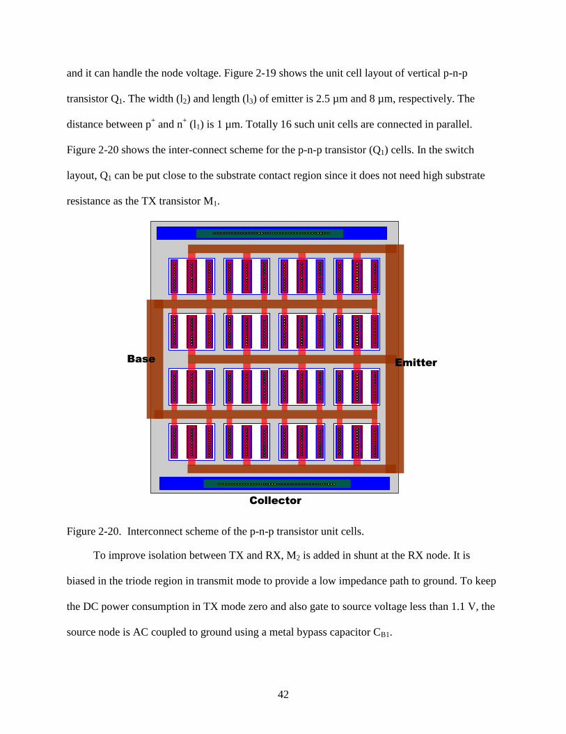
and it can handle the node voltage. Figure 2-19 shows the unit cell layout of vertical p-n-p
transistor Q1. The width (l2) and length (l3) of emitter is 2.5 µm and 8 µm, respectively. The
distance between p+ and n
+ (l1) is 1 µm. Totally 16 such unit cells are connected in parallel.
Figure 2-20 shows the inter-connect scheme for the p-n-p transistor (Q1) cells. In the switch
layout, Q1 can be put close to the substrate contact region since it does not need high substrate
resistance as the TX transistor M1.
BaseEmitter
Collector
Figure 2-20. Interconnect scheme of the p-n-p transistor unit cells.
To improve isolation between TX and RX, M2 is added in shunt at the RX node. It is
biased in the triode region in transmit mode to provide a low impedance path to ground. To keep
the DC power consumption in TX mode zero and also gate to source voltage less than 1.1 V, the
source node is AC coupled to ground using a metal bypass capacitor CB1.
43
The T/R switch working in receive mode is shown in Figure 2-21. The TX transistor M1 is
off, and diode D1 and vertical p-n-p transistor, Q1 are forward biased. There is DC current
flowing through the biasing path which consists of L1, L2, D1 and Q1. This establishes a low
impedance path between ANT and RX ports. A metal by-pass capacitor (CB3) is also integrated
to bypass the noise from Q1. If narrow-band response is acceptable, L1 and L2 can be replaced by
an on-chip tuned LC circuits to make the diode T/R switch fully integrated.
TX
ANT
VG1
Rsub
VB
M1
D1
RX
Q1
L1
L2
VG2
M2
Vbias3
CB1
CB2
CB3
Vbias1 Vbias2
P N
P1
N1
Vbias4
RF Signal
DC Current
Figure 2-21. T/R switch operation in receive mode.
Table 2-1 lists the bias voltages for the switch in transmit and receive modes. Despite the
voltages are significantly higher than normal in 45 nm CMOS circuits, the voltages across gate
oxide are within the safe operating region. For instance, when M2 is off in RX mode, VG2 and
gate-to-body voltage are 4 V. However, because of the depletion region under the gate oxide, the
voltage across the gate oxide should be less than 1.2 V.

44
Table 2-1 Transmit/Receive (T/R) switch bias voltages in transmit/receive mode
Bias Nodes Bias Voltage (V)
Transmit Mode
Bias Voltage (V)
Receive Mode
Vbias1 0 5.4
Vbias2 4.7 4.5
Vbias3 4.7 4.5
Vbias4 0 5.4
VG1 1 5.4
VG2 6 4
VB 4.7 3.7
The simulated input 1 dB compression points of the T/R switch working at transmit mode
at 900 MHz is ~28 dBm. Figure 2-22 shows the gate-source and gate-drain voltage waveforms of
transistors M1 and M3 when the T/R switch is running at 1 dB input compression point in
transmit mode at 900 MHz. The waveforms are extracted from harmonic balance simulations.
Even though the time axis is started from 0, they are already in a steady state. As we can see all
the peak voltages are smaller than 1.2 V. This means that the reliability issue for the transistors
can be neglected.
0.0 0.5 1.0 1.5 2.0-1.5
-1.0
-0.5
0.0
0.5
1.0
1.5
VSG1
VGD1
VDG2
VGS2
Vo
lta
ge
(V
)
Time (ns)
Figure 2-22. Gate-source and gate-drain voltage waveforms of transistors M1 and M2 when T/R
switch input power is 28 dBm.

45
The NMOS/Diode hybrid T/R switch is fabricated in a 45 nm CMOS technology which
supports only low leakage transistors and seven metal layers. The top copper layer thickness is
~1.5 μm. The test chip was mounted on a printed circuit board with DC biasing. Two external
chip inductors L1 and L2 are also soldered on the board. The photo of evaluation board and the
test chip is shown in Figure 2-23. The total area including the bond pads of the switch is
~0.82×0.76 mm2.
L1 L2
P1 N1
P N
TX RX
P1 N1
P N
ANT
Figure 2-23. Die photo of the NMOS/Diode hybrid T/R switch in 45 nm CMOS.

46
2.2.3 Measurement Results
As mentioned, the p-n diode D1 in Figure 2-17 forms a parasitic p-n-p transistor with the
substrate acting as a collector when it is forward biased. Figure 2-24 shows the T/R switch
working in receive mode including the parasitic p-n-p transistor of D1. The parasitic p-n-p
transistor associated with D1 and the p-n-p transistor Q1 used in the biasing circuit are measured
and characterized to check their impact on the switch performance.
TX
ANT
VG1
Rsub1
M1
L1
CB2
Vbias1
P
P1
Vbias4
VB
RX
Q1
L2
VG2
M2
Vbias3
CB1
CB3
Vbias2
N
N1
Rsub2
(Emitter)
(Base)
IE
IB
IC
Figure 2-24. T/R switch in receive mode including the parasitic p-n-p associated with D1.
To measure the DC characteristic of parasitic vertical p-n-p transistor associated with D1,
the device was connected to a semiconductor DC parameter analyzer. It should be noted that the
substrate resistance Rsub2 between the collector of the parasitic p-n-p and body contact is also
included in the DC measurement. The measured DC characteristics are shown in Figure 2-25.

47
The current gain β is approximately 1. When base current IB is 1 mA and VCE is bigger than 3 V,
the parasitic p-n-p is in the forward bias region. While when IB is larger than 2 mA and VCE is
smaller than 5 V, the transistor is in saturation region. In order to reduce the signal loss through
this parasitic shunt path, Vbias2 is set to 4.5 V and Vbias4 is set to 5.4 V in receive mode such that
the n-well to substrate capacitance is reduced. Figure 2-26 shows the DC characteristics of p-n-p
transistor Q1, which has peak current gain of approximately 8. Since Q1 is put close to the
substrate contact, the associated substrate resistance is small.
Three GS/SG probes with 150 μm pitch were used for all the RF measurements. One of the
three ports was terminated with a 50 Ω load through a bias tee during two port S-parameter
measurements using an HP8510C network analyzer. The measurement setup is illustrated in
Figure 2-26.
0 1 2 3 4 50.0
0.5
1.0
1.5
2.0
2.5
3.0 I
B=6mA
IB=7mA
IB=8mA
IB=9mA
IB=10mA
IB=1mA
IB=2mA
IB=3mA
IB=4mA
IB=5mA
I C (
mA
)
Vce
(V)
Figure 2-25. Measured DC characteristics of the parasitic vertical p-n-p transistor associated
with D1.

48
0.0 0.2 0.4 0.6 0.8 1.00
2
4
6
8
10
IB=1.3mA
IB=1.5mA
IB=1.7mA
IB=1.9mA
IB=0.1mA
IB=0.3mA
IB=0.5mA
IB=0.7mA
IB=0.9mA
IB=1.1mA
I C (
mA
)
Vce
(V)
Figure 2-26. Measured DC characteristics of the p-n-p transistor Q1.
DC power supply
50Ω
RF probe
RF probe
Spectrum analyzer
Figure 2-27. T/R switch measurement setup.

49
Figure 2-28 shows the measured insertion loss. At 900 MHz, insertion loss for RX and TX
are 0.5 dB and 1.1 dB respectively. The plot also shows the noise figure of switch in RX mode.
The noise figure is almost the same as the insertion loss indicating the noise of forward biased
diode and Q1 can be managed. In RX mode, the DC bias current is 5 mA. Around 2.5 mA flows
between the anode and cathode.
0.9 1.0 1.1 1.20.0
0.5
1.0
1.5
2.0
No
ise F
igu
re (
dB
) Noise Figure
RX
Inse
rtio
n L
oss (
dB
)
Frequency (GHz)
TX
Figure 2-28. Measured insertion loss of the T/R switch.
Isolation and return loss of the T/R switch are shown in Figure 2-29. In TX mode, the
return loss is less than -15 dB and the isolation between TX and RX ports is better than 25 dB
from 900 MHz to 1.2 GHz. In RX mode, the return loss is less than -21 dB and isolation between
ANT and TX ports is better than 17 dB from 900 MHz to 1.2 GHz.
Power compression measurements were carried out using a signal generator together with
an external power amplifier and a power meter. The power losses from the measurement set-up
and cable were de-embedded. Figure 2-30 shows the output power versus input power plot at 900
MHz. IP1dB is 27.8 dBm and IIP3 is 42.5 dBm. To examine the reliability of switch, the T/R
switch was stressed at 30 dBm input power when the ANT pad was left open. The measured S-

50
parameters showed no difference before and after the stress. The performance of the proposed
NMOS/Diode hybrid T/R switch is summarized in Table 2-2. And the performance comparison
of this design with the previously published CMOS T/R switches is listed in Table 2-3.
0.9 1.0 1.1 1.2-35
-30
-25
-20
-15
-10
-5
0
Frequency (GHz)
0
5
10
15
20
25
30
RX
TX
TX
RX
Is
ola
tio
n (
dB
)
Re
turn
Lo
ss
(d
B)
Figure 2-29. Measured return loss and isolation of the T/R switch.
-10 0 10 20 30 40
-80
-60
-40
-20
0
20
40
IIP
3=
42.5
dB
m
IP1
dB=
27.8
dB
m
Ou
tpu
t P
ow
er
(dB
m)
Input Power (dBm)
Figure 2-30. Measured output power versus input power plot of the T/R switch. IP1dB is 27.8
dBm.

51
Table 2-2 Measured NMOS/Diode hybrid T/R switch performance summary
Specifications Measured Results
Frequency 900 MHz
Insertion Loss (Transmit Mode) 0.5 dB
Insertion Loss (Receive Mode) 1.1 dB
Isolation (Transmit Mode) 27.5 dB
Isolation (Receive Mode) 15 dB
IP1dB for Transmit Mode 27.8 dBm
IIP3 for Transmit Mode 42.5 dBm
Power Consumption 27 mW
Chip Area 0.6 mm2
Table 2-3 Performance comparison to the previously published CMOS T/R switches
Frequency
(GHz)
TX IL
(dB)
RX IL
(dB)
TX
Isolation
(dB)
RX
Isolation
(dB)
Linearity
(dBm)
CMOS
Technology
Chip
Area
(mm2)
Ref.
2.5 1.1 - 32 - 34
IP1dB
32 nm - [31]
2.4 0.4 0.2 30 16 30
IP1dB
90 nm 0.02 [30]
5 0.9 0.9 27 17 31
IP1dB
90 nm 0.2 [28]
2.4 1.5 1.6 32 17 28.5
IP1dB
0.18 µm 0.56 [25]
0.9 0.5 1.0 37 29 31.3
IP1dB
0.13 µm
Triple well
0.11 [26]
1.8 0.75 1.1 20 35 33
IP0.1dB
0.18 µm
Triple well
0.4 [29]
1.9 1.5 1.9 18 32 33.5
IP0.3dB
0.18 µm
Triple well
0.4 [27]
2.4 0.7 0.7 35 35 21.3
IP1dB
0.18 µm
0.03
[22]
0.9 0.5 1.1 27.5 15 27.8
IP1dB
45 nm 0.6 This
work

52
2.3 Conclusions
Compared to MOS transistors in nano-scale CMOS, p-n diodes have the advantage of high
breakdown voltage. Use of a p+-n-well diode in a T/R switch operating around 900 MHz has
been evaluated. TX and RX insertion loss of 0.5 dB and 1.1 dB, and IP1dB of ~28 dBm have been
achieved in a 45 nm bulk CMOS process using a series NMOS and series diode hybrid
configuration. Only thin-gate-oxide transistors along with p-n diode are used. Presently, IP1dB is
limited by the breakdown voltage of the diode, and this needs to be increased. Impedance
transformation using on-chip networks can also be used to increase IP1dB for narrow band
applications. To fulfill the promise for broadband operation of switch, the n-well to p-substrate
junction capacitance should be further reduced. Generating the necessary bias voltage
complicates the use of switch, although many systems have higher voltages available for display
and other subsystems. Lastly, the switch requires DC power consumption in RX mode, and
approaches to lower this including further reduction of current gain of parasitic p-n-p transistors
are needed. This is the first effort to evaluate the performance can be achieved of a T/R switch
operating around 900 MHz using p-n diodes in nano-scale CMOS.

53
CHAPTER 3
2.4-GHZ CMOS CLASS-F POWER AMPLIFIER
3.1 Overview
3.1.1 Radio Frequency (RF) Power Amplifier (PA) Specification Parameters
RF power amplifier requirement depends on standards and applications. The key
specifications of power amplifiers include output power, power gain, efficiency, and linearity
[5], [34], [35], [36]. They will be introduced in this section.
3.1.1.1 Output power and power gain
Figure 3-1 shows a basic power amplifier connected to the load impedance RL. The output
power is defined as the active power delivered by the power amplifier and flowing into the load
impedance, which is commonly 50 Ω. The instantaneous output power is defined as
( ) ( ) ( )o out outp t v t i t
(3-1)
In most cases, only the power at fundamental frequency is wanted, and all the other harmonic
power will be filtered or suppressed. Assuming the amplitude of fundamental output voltage is
VO, the output power at fundament frequency is
2
2
oout
L
VP
R
(3-2)
Finite input power (Pin) is required to drive the power amplifier. From Figure 3-1, the power gain
is defined as
, 1010log ( )outP dB
in
PG
P
(3-3)
3.1.1.2 Efficiency
Efficiency of power amplifiers defines how efficient the circuit uses the DC power to
deliver output power to the load. The DC power consumption PDC,PA in Figure 3-1 will be always
larger than output power Pout. Drain efficiency ηdrain of PA is defined as

54
,
outdrain
DC PA
P
P
(3-4)
To take input power into consideration, the power added efficiency (PAE) is introduced as
,
out in
Dc PA
P PPAE
P
(3-5)
By using equation (3-3), PAE can be rewritten as
,
(1 )1
(1 )
inout
outdrain
DC PA p
PP
PPAE
P G
(3-6)
The above equation shows that when the power gain of PA is large enough, drain efficiency is
approximately the same as power added efficiency.
VDD
PA
RL
PinPout
PDC,PA
IN OUT
iout
vout
Figure 3-1. Definition of PA output power, power gain and efficiency.
In most power amplifier designs, driver stages are needed between the input source and the
PA output stage. Figure 3-2 shows a power amplifier with two driver stages. Those driver stages
will also consume DC power. Considering the power consumption of driver stages, the overall
efficiency of the power amplifier can be defined as

55
_ _ ,
1
outoverall n
DC PA DC DRV i
i
P
P P
(3-7)
The more driver stages are used, the higher power gain of the entire power amplifier, but the
lower of the overall efficiency. The power added efficiency in this situation will be defined as
_ _ ,
1
out in
n
DC PA DC DRV i
i
P PPAE
P P
(3-8)
During the practical power amplifier design, the number of driver stages is decided by power
gain, linearity and efficiency requirements of the PA.
VDD_PA
PA
RL
Pin Pout
PDC,PA
IN
OUT
iout
vout
DRV2DRV1
VDD_DRV2VDD_DRV1
PDC,DRV2PDC,DRV1
Figure 3-2. Definition of PA efficiency with driver stages.
3.1.1.3 Linearity
Linearity of a power amplifier can be defined in phase linearity and amplitude linearity.
When bandwidth of the modulated signal is small compared with the carrier frequency, phase
linearity is easy to achieve. Phase nonlinearity or phase distortion is denoted as PM-PM
distortion. Amplitude nonlinearity or amplitude distortion is denoted as AM-AM distortion. So in

56
constant envelop systems, PA needs to have good phase linearity while amplitude linearity is not
a big issue, whereas in other communication systems such as W-CDMA, which has varying
envelope signals, good amplitude linearity is also required.
Power amplifier linearity can also be characterized by third order intercept point (IP3)
which is based on two-tone signal test and gives the output power for which the third order inter-
modulation term becomes as large as fundamental output power. But in modern communication
systems, for power amplifier, IP3 is not usually specified. Instead a spectral mask, error vector
magnitude and adjacent channel power are used.
3.1.2 Power Amplifier Classification
3.1.2.1 Class A, AB, B and C power amplifier
The general power amplifier model which could be used to study class A, AB, B and C
power amplifiers in shown in Figure 3-3. A high Q LC tank is resonated at fundamental
frequency and short all the other high order harmonics. The above four types of power amplifiers
are distinguished by bias conditions.
RFC
VDD
CB
C L RL
VO
Vin
+
M1
IDC
-
Rbias
Vbias
VDS
Figure 3-3. General power amplifier model.

57
In a Class-A power amplifier, the transistor operates linearly across the full input and
output range, and there is always current flowing through the output transistor. The device will
remains at all times in the transconductance region, which means that the voltage never falls
below the knee voltage. The drain voltage and current waveforms for Class-A power amplifier is
shown in Figure 3-3. The output swing VO is maximized as VDD if the quiescent current through
the transistor is equal to VDD/RL. The efficiency for Class-A power amplifier is obtained as
21( )
2
O O
DC DD
P V
P V
(3-9)
And the maximum output power of Class-A power amplifier related to the maximum drain-
source voltage VDS,max can be expressed as
2
,max
,max
1
8
DS
O
L
VP
R
(3-10)
According to equation (3-9), 50% maximum drain efficiency can be achieved for Class-A power
amplifier. If knee voltage VK of the transistor is also considered, the maximum drain efficiency
of Class-A power amplifier can be expressed as [36]
,max
max
,max
11
2 1
K DS
K DS
V V
V V
(3-11)
t
Drain
current
Drain
voltage
Figure 3-4. Drain voltage and current waveforms for Class-A power amplifier.

58
In a Class-AB power amplifier, the transistor conducts more than half of the cycle, in a
Class-B power amplifier, the transistor conducts half of the cycle, and in a Class-C power
amplifier, the transistor is on for less than half of the cycle. They can also be classified using
conduction angle θ which represents the total number of radians during the cycle when the
device is conducting. The drain efficiency is as follow [34]
,max
max
,max
11 sin( )
2 1 2sin( 2) cos
K DS
K DS
V V
V V
(3-12)
Figure 3-5 to Figure 3-7 show the drain voltage and current waveforms for Class-AB, B and C
power amplifiers.
t
Drain
current
Drain
voltage
Figure 3-5. Drain voltage and current waveforms for Class-AB power amplifier.
t
Drain
current
Drain
voltage
Figure 3-6. Drain voltage and current waveforms for Class-B power amplifier.

59
t
Drain
current
Drain
voltage
Figure 3-7. Drain voltage and current waveforms for Class-C power amplifier.
3.1.2.2 Saturated transconductance amplifier
For a reduced conduction angle power amplifier such as Class-AB, B and C mentioned in
section 3.1.2.1, the transistor will be turned off for a certain amount of time, which depends on
the gate bias voltage and input RF amplitude. This reduces the current-voltage overlap, resulting
in a higher efficiency. On the other side, the output power of the amplifier will be reduced.
t
Drain
current
Drain
voltage
Figure 3-8. Drain voltage and current waveforms for overdriven Class-A power amplifier.
If the gate bias of the power amplifier is not changing, but the amplitude of the input
voltage is increased, the output of the power amplifier will be no longer sinusoid and clipping
behavior will be show up. This over-driven effect will also reduce the overlap between drain

60
voltage and current. Therefore the efficiency will be increased, along with degraded input to
output linearity. Figure 3-8 and 3-9 show the drain voltage and current waveforms of overdriven
or saturated Class-A and Class-B power amplifiers.
t
Drain
current
Drain
voltage
Figure 3-9. Drain voltage and current waveforms for overdriven Class-B power amplifier.
3.1.2.3 Class-D power amplifier
Vin
C L
RL
VDD
Figure 3-10. Schematic of Class-D power amplifier.

61
A schematic of Class-D power amplifier is shown in Figure 3-10. The input signal is
square wave, and the transistors are working in a switch mode. Ideally, there is no loss in the
switch, and a high Q LC resonant circuit also make sure only the fundamental signal will be
delivered to the load, and no harmonic power are dissipated on the load. So, for an ideal Class-D
power amplifier, 100% drain efficiency can be achieved. Figure 3-11 shows the drain voltage
and current waveforms for ideal Class-D power amplifier.
t
Drain
current
Drain
voltage
Figure 3-11. Drain voltage and current waveforms of Class-D power amplifier.
3.1.2.4 Class-E power amplifier
Vout
RL
Vin
C0 L0Lx
L
C1
VDD
Vds
Figure 3-12. Schematic of Class-E power amplifier.

62
Similar to Class-D, a Class-E power amplifier is also a switch-mode amplifier which could
achieve ideally 100% drain efficiency. The basic circuit is shown in Figure 3-12 [21]. The
NMOS transistor works as a switch and the high Q series LC tank forms a harmonic filter which
is tuned at fundamental frequency. Figure 3-13 shows the drain voltage and current waveforms
for Class-E power amplifier [37], [38], [39].
t
Drain
current
Drain
voltage
Figure 3-13. Drain voltage and current waveforms for Class-E power amplifier.
The Class-E power amplifier is entirely designed in the time domain. Assume L is a RF
chock, when the switch is ON, the DC current from the inductor L will flow through the switch.
When the switch is OFF, the DC current minus the sinusoidal output current will be dumped into
the capacitor C1. To ensure 100% efficiency, the power consumption of the transistor must be
zero, which means that the drain current and voltage cannot be non-zero at the same time. All
component values are chosen to make transistor drain voltage satisfy the following conditions
[37], [38], [39]:
1. As the switch turns off, drain voltage remains low long enough for the current to drop to
zero.
2. Drain voltage reaches to zero before the switch tunes on.
3. dVds/dt is also near zero when the switch turns on.

63
The second condition prevents dissipation of the energy stored by the shunt capacitor at turn-on,
and the third condition makes the circuit less sensitive to components, frequency and switching
variations. To satisfy these, values of inductor and capacitor must be
1.1525 Lx
RL
(3-13)
0.1836
L
CR
(3-14)
A drawback of Class-E power amplifier is the large peak voltage that the switch sustains
in the off state, which is 3.56VDD in the ideal case. This means that high transistor breakdown
voltage or stacked transistor is needed [40], [41], [42], [43]. This is a critical issue especially
when the power amplifier is implemented in advanced CMOS processes with low transistor
breakdown voltage. Assume the drain voltage cannot exceed 2VDD for reliable operation of the
power amplifier, the maximum output power for Class-E PA is
2
,max, 0.182 DDo Class E
L
VP
R (3-15)
RL is the nominal load impedance.
3.1.2.5 Class-F power amplifier
Power amplifier efficiency can also be improved by using harmonic tuning. Figure 3-14
shows the schematic of generic Class-F power amplifier. At the fundamental frequency, the
impedance looking into the resonator is the optimized resistance Ropt. At odd order harmonic
frequencies, the impedance is ideally infinity, and at even order harmonic frequencies the
resonator impedance is zero. Under the above harmonic tuning conditions, the drain voltage and
current would be square wave and half sine wave respectively, with 180 degree phase difference
as shown in Figure 3-15. 100% drain efficiency can be achieved in an ideal Class-F power
amplifier. If the load harmonic impedance is only considered to third order harmonics, the ideal
drain efficiency is 88.4%, and 92% for fifth order harmonic termination [44], [45]. Similarly as

64
we discussed for Class-E PA, if the drain voltage cannot exceed 2VDD, the maximum output
power for Class-F power amplifier with third and fifth harmonic termination network are as
follows [35], [44], [45]:
2
,max, 3 0.6328 DDo Class F
L
VP
R (3-16)
2
,max, 5 0.6868 DDo Class F
L
VP
R (3-17)
Vin
Resonator
RL
RFC
VDD
Z1=Ropt
ZO=∞
ZE=0
M1
Figure 3-14. Schematic of generic Class-F power amplifier.
t
Drain
current
Drain
voltage
Figure 3-15. Drain voltage and current waveforms of Class-F power amplifier.

65
3.2 2.4-GHz CMOS Class-F Power Amplifier Design
Class-E and Class-F are two commonly used in high efficiency non-linear PAs. A Class-E
PA is more efficient because of hard switching and zero voltage switching as mentioned in the
last section, and easier to build because of the relatively simple output network compared with
Class-F power amplifier. However, for this operation, the drain voltage can be as high as 3.6VDD,
which can stress the MOS transistor. This is especially severe in advanced CMOS technologies.
On the other hand, in a Class-F PA, though the output matching network is more
complicated, the PA transistor experiences peak voltage of only 2VDD. In order to decrease the
loss from matching networks, most of the published Class-F CMOS PAs use either an off-chip
transmission line or bond wire inductors [46], [47], [48], which are not preferable for a true
single chip radio integrating an on-chip antenna. In this section, a fully integrated 2.4 GHz Class-
F CMOS PA for the true single chip radio fabricated in the UMC 130 nm digital CMOS process
with eight-layer copper metallization is introduced.
Table 3-1 Maximum efficiency of Class-F power amplifier under different harmonic
termination conditions
n=1 n=3 n=5 n=∞
50% 57.74% 60.33% 63.7%
m=2 70.7% 81.65% 85.32% 90.03%
m=4 74.97% 86.56% 90.45% 95.45%
m=∞ 78.5% 90.69 94.77% 100%
To implement the output network for Class-F PA, ideally an infinite number of inductors
and capacitors are needed. Since the quality factor of on-chip inductors is not high, including
multiple inductors increases loss. So, having higher order harmonic networks does not mean
higher efficiency, not to mention an increased circuit area. Table 3-1 lists the maximum output
efficiency for Class-F power amplifier for given set of harmonics [44], [45]. The efficiency
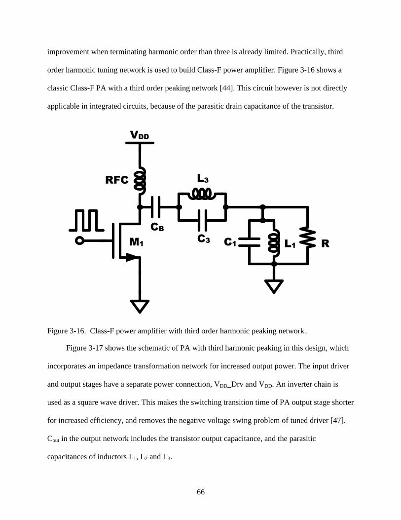
66
improvement when terminating harmonic order than three is already limited. Practically, third
order harmonic tuning network is used to build Class-F power amplifier. Figure 3-16 shows a
classic Class-F PA with a third order peaking network [44]. This circuit however is not directly
applicable in integrated circuits, because of the parasitic drain capacitance of the transistor.
C1
L3
L1
C3
CB
RFC
VDD
RM1
Figure 3-16. Class-F power amplifier with third order harmonic peaking network.
Figure 3-17 shows the schematic of PA with third harmonic peaking in this design, which
incorporates an impedance transformation network for increased output power. The input driver
and output stages have a separate power connection, VDD_Drv and VDD. An inverter chain is
used as a square wave driver. This makes the switching transition time of PA output stage shorter
for increased efficiency, and removes the negative voltage swing problem of tuned driver [47].
Cout in the output network includes the transistor output capacitance, and the parasitic
capacitances of inductors L1, L2 and L3.

67
VDD_PA
RL
Vin
VDD_Drv
Cout
L1
L2
C2
L3
C3
C4
CB
Rf
L4
Ropt
C4
@ fundamental
frequency
MPAMn1 Mn2 Mn3 Mn4
Mp1 Mp2 Mp3 Mp4
Figure 3-17. Schematic of the fully integrated Class-F PA in this design.
The impedance looking into the output network should be zero at the second order
harmonic frequency and open at the third order harmonic frequency. L2 and C2 form a series
resonant circuit which shorts out the network at second order harmonic frequency. A way to
make the network open at the third harmonic frequency is to resonate L3 and C3 at the frequency
[49], [50]
2 2 01/ 2L C (3-18)
3 3 01/ 3L C (3-19)
Additionally, the impedance of peaking network including L1, L2, C2 and Cout should also be
open at the third order harmonic frequency
0 1 0 2
0 0 2
1 13 || || ( 3 )
3 3out
j L j Lj C j C
(3-20)
At the fundamental frequency, the impedance of peaking network including L1, L2, C2 and Cout
should also be infinite.
0 1 0 2
0 0 2
1 1|| || ( )
out
j L j Lj C j C
(3-21)

68
In this case, the load impedance looking from the drain of the PA transistor at fundamental
frequency will be only decided by the combination of L3, C3, C4 and RL. The L3 and C3 parallel
circuit is inductive at the fundamental frequency. This equivalent inductance L4 along with
capacitor C4 will make the L-shape impedance transformation network as shown in the inset of
Figure 3-17. When the load impedance is transformed from RL to ROPT, the values of L4 and C4
should be
4
0
1L
L
R RL
R
(3-22)
4
0
11
L
RC
R R
(3-23)
The values of L3 and C3 are adjusted to make their equivalent inductance at the fundamental
frequency equal to L4 of the impedance transformation network.
0 3 0 4
0 3
1||j L j L
j C
(3-24)
From equations (3-18), (3-21) and (3-23), L3 and C3 should be
3
0
81
9
L
L
R RL
R
(3-25)
3
0
1
8 1L
L
CR
RR
(3-26)
From equations (3-18), (3-20) and (3-21), the values of L1, L2 and C2 are [49]
1 2
0
4
9 out
LC
(3-27)
2 2
0
4
15 out
LC
(3-28)
2
15
16outC C (3-29)
Once Cout and Ropt are known, the values of all the components are specified. Figure 3-18 shows
the equivalent circuit of the Class-F PA output matching network working at fundamental,
second and third-order frequencies.

69
VDD_PA
RLCout
C4
CB
L4
Ropt
MPA
C3
L3
From PA driver
Resonate at fundamental
frequency
L1
L2
C2
A
Resonate at second-
order harmonic
frequency
VDD_PA
RL
Cout
C4
CB
MPA
From PA driver
L1
L2
C2
C3
L3
B VDD_PA
RL
Cout
C4
CB
MPA
From PA driver
Resonate at third-order
harmonic frequency
L1
L2
C2
C3
L3
C
Figure 3-18. Equivalent circuit of the Class-F PA output matching network working at A)
fundamental frequency, B) second-order frequency and C) third-order frequency.

70
To handle the output current, the PA output transistor size should be sufficiently wide. On
the other hand, a wider transistor has larger parasitic capacitances. From load-pull simulations,
the optimum width and length of PA transistor are 250 µm and 0.12 µm, with each finger width
of 1 µm. The output capacitance Cout approximately equals to Cdb+Cgd. As previously mentioned,
Cout should be accurately estimated to set the component values in the output network. The
parasitic capacitance of metal lines for transistor connections is non-negligible and should be
accounted. The poly-silicon gate is contacted from both sides to decrease the gate resistance.
Since the transistor source is grounded, the source diffusion length is increased to 0.56 µm. This
increases the separation between the source and drain metal connections and that between the
source and poly-silicon gate connections, which in turn reduces the parasitic capacitance. Figure
3-19 shows the layout cell of PA output transistor.
Source
(Metal 1)
Drain
(Metal 1~6)
0.22µm0.12µm
0.56µm
Gate
(Metal 3)
1µm
Active
Poly
Contact/Via
Figure 3-19. Layout cell of the PA output transistor.

71
0.0 0.2 0.4 0.6-20
0
20
40
60
80
100
Dra
in V
olta
ge
VDD_PA (V)
Dra
in C
urr
en
t (m
A)
0.0
0.5
1.0
1.5
2.0
2.5
3.0
Figure 3-20. Simulated drain voltage and current waveforms of the Class-F power amplifier
with third order harmonic peaking.
Table 3-2 The transistor sizes and passive component values of the Class-F power amplifier
Device Value Device Value
Mn1 21 µm/0.12 µm Mp1 63 µm/0.12 µm
Mn2 3 µm/0.12 µm Mp2 9 µm/0.12 µm
Mn3 9 µm/0.12 µm Mp3 27 µm/0.12 µm
Mn4 27 µm/0.12 µm Mp4 81 µm/0.12 µm
MPA 250 µm/0.12 µm Rf 140 Ω
L1 2.2 nH L2 1.3 nH
L3 1.3 nH C2 820 fF
C3 360 fF C4 870 fF

72
The transformed resistance at the fundamental frequency, Ropt in Figure 3-17 depends on
the target output power and efficiency. There is tradeoff between the output power and
efficiency. To increase the output power, Ropt should be smaller. This however lowers the
efficiency because the ratio between the series resistance of inductor and Ropt increases and the
loss of impedance transformation network increases. Since it is for short-range wireless sensor
application, in this design, the target output power is 10 dBm. The maximum voltage at the drain
node is set by the transistor breakdown and reliability limit. For VDD_PA=1.2V, RL of 40 Ω is
chosen to maximize the efficiency (with 2 dBm output power margin) and set the maximum
drain voltage at 2.4 V. The transistor sizes and passive component values of the proposed Class-
F power amplifier are listed in Table 3-2. Figure 3-20 shows the simulated drain voltage and
current waveforms of the proposed Class-F power amplifier with third order harmonic peaking
network.
The quality (Q) factor of on-chip inductor is critical. In order to analyze the impact of Q of
different inductors on PA efficiency, Q for each inductor is swept in simulations while the other
inductors are assumed to be ideal. The plot is shown in Figure 3-21. Drain efficiency of 81% can
be achieved when all the inductors are ideal. The drain efficiency is most sensitive to the Q of
inductor L1. To increase Q of inductor, the top two copper metal layers and Al-cap aluminum
layer are shunted to form the inductor L1, L2 and L3. The metal width is chosen to be 10 µm. The
metal trace is ~4µm above a poly-silicon patterned ground shield. From ADS Momentum
simulations, the quality factors of L1, L2 and L3 at 2.4 GHz are 7.6, 7 and 5, respectively. The
inductor Q is limited by the top metal thickness, and the PA efficiency can be further improved
by thickening the metal layer. The simulated drain efficiency with these inductors is 51%.

73
0 5 10 15 20 25 30 35 40 45
50
55
60
65
70
75
80
Dra
in e
ffic
ien
cy (
%)
Inductor Q
L1
L2
L3
Figure 3-21. Simulated drain efficiency versus Q for different inductors.
3.3 Measurement Results
The PA output is connected to a power meter through an HP8495A 50 MHz-26.5 GHz
power sensor. The measurement setup is illustrated in Figure 3-22. The power losses from the
measurement set-up and cable are de-embedded. The measured return loss is less than -32 dB in
the frequency range of 2 to 3 GHz. The PA output power is saturated when input power is larger
than -1.5 dBm. The maximum saturated power gain is about 13.9 dB. Figure 3-23 shows the
measured saturated PA output power, drain efficiency and power added efficiency (PAE) versus
VDD_PA. VDD_Drv is kept at 1.2 V with 7 mA DC current. Output power of 12.4 dBm is
measured at VDD_PA=1.2 V with drain efficiency (ED) of 46.5% when only the PA stage is
considered, and PAE of 38% for the entire PA including the driver. The DC current in the power
stage is 31 mA. When VDD_PA is increased while VDD_Drv is kept constant, the drain efficiency
of PA stage decreases because the transistor spends more time in saturation region which

74
increases effective loss of PA transistor. On the other hand, the PAE of entire PA increases with
VDD_PA because the increased output power (Pout) overcomes the decreased drain efficiency
(equation (3-30)). Figure 3-24 shows the measured saturated PA output power, drain efficiency
and PAE versus input frequency at 1.2 V DC supply voltage for the entire amplifier including the
driver stage. The output power and efficiencies are peaked around 2.4 GHz. The die photograph
of circuit is shown in Figure 3-25. The chip size is 0.6 mm x 0.7 mm including bond pads. Table
3-3 lists the performance summary of the PA and the comparisons with preciously published
CMOS Class-F PA’s are shown in Table 3-4.
DC power supply
RFin
Spectrum Analyzer
RFout
RF probe
DC probe
Signal generator
Figure 3-22. Measurement setup for the PA power measurement.
1
1( )
out in
DrvPA Drv
D out
P PPAE
PP P
E P
(3-30)
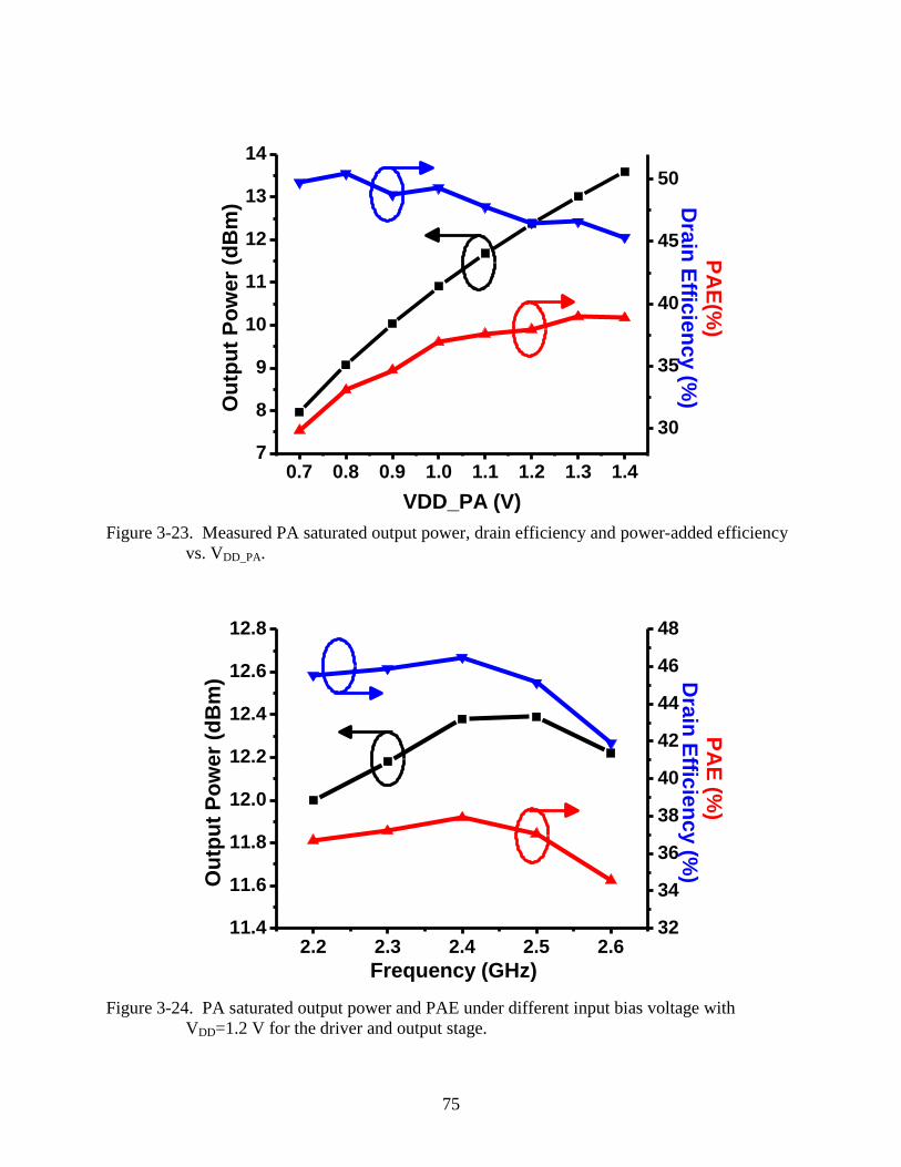
75
0.7 0.8 0.9 1.0 1.1 1.2 1.3 1.47
8
9
10
11
12
13
14
PA
E(%
)
VDD_PA (V)
Ou
tpu
t P
ow
er
(dB
m)
30
35
40
45
50
Dra
in E
fficie
ncy (%
)
Figure 3-23. Measured PA saturated output power, drain efficiency and power-added efficiency
vs. VDD_PA.
2.2 2.3 2.4 2.5 2.611.4
11.6
11.8
12.0
12.2
12.4
12.6
12.8
Dra
in E
fficie
ncy (%
)
Frequency (GHz)
Ou
tpu
t P
ow
er
(dB
m)
32
34
36
38
40
42
44
46
48
PA
E (%
)
Figure 3-24. PA saturated output power and PAE under different input bias voltage with
VDD=1.2 V for the driver and output stage.

76
L1
L2
L3
In Out
C2
C3
Figure 3-25. Die micrograph of the Class-F power amplifier.
Table 3-3 Performance summary of the Class-F PA in this design
Frequency
(GHz)
VDD
(V)
IDrv
(mA)
IPA
(mA)
Psat
(dBm)
Gain
(dB)
Drain
efficiency (%)
PAE
(%)
Area
(mm2)
2.4 1.2 7 31 12.4 13.9 46.5 38 0.42
Table 3-4 Performance comparison to the previously published CMOS Class-F PA
Reference [47] [48] [51] This work
Frequency (GHz) 0.9 1.9 5.6 2.4
VDD (V) 1.8/3.0 3 1.9 1.2
Pout (dBm) 31.7 22.8 18.4 12.4
PAE/ED (%) 43/- 42/56 42.8/49.2 38/46.5
Technology 0.2 μm 0.6 μm 0.18 μm 0.13 μm
Area (mm2) 2 - 1.1 0.42
Fully integrated No No Yes Yes

77
3.4 Conclusions
The classification of power amplifiers is introduced in this chapter, and a fully integrated
2.4-GHz Class-F power amplifier fabricated in the UMC 130 nm single poly-silicon and eight
metal layer digital CMOS process is demonstrated. The single-ended power amplifier consists of
a tapered inverter driver with wideband resistive feedback input matching and an output stage
with a fully integrated third harmonic peaking network incorporating impedance transformation.
The drain efficiency and PAE are 46.5% and 38% respectively at 1.2 V supply voltage, and the
saturated output power is 12.4 dBm with 13.9 dB saturated power gain. The performance of PA
from this work is compared to that of the previously published CMOS Class-F PA’s in Table 3-1.
To the best knowledge of authors, the 2.4 GHz operation frequency is the lowest at which full
integration of Class-F PA in CMOS is demonstrated.

78
CHAPTER 4
MULTI-BAND WATT-LEVEL CMOS POWER AMPLIFIER
4.1 Overview
4.1.1 Design Challenges of Watt Level Power Amplifier in Nano-Scale CMOS
Implementing a power amplifier with watt-level output power in a CMOS technology is
challenging, especially in more advanced technology nodes such as 65nm and 45nm CMOS
technology with low supply voltage. Unlike a GaAs HBT process, an LDMOS process and a
SiGe HBT process which can provide fast and higher breakdown voltage transistors, the 65 nm
CMOS technology used in this design supports lower breakdown voltage transistors. Because of
the high output power requirement, the reliability limit is often pushed in the design of CMOS
power amplifiers. It is suggested that keeping the voltage swing at each node of the transistor
below twice the nominal supply voltage will cause no reliability issue [35], [52], [53], [54], [55],
[56].
The breakdown and stress-related degradation mechanisms in MOS transistors include gate
oxide breakdown, hot carrier degradation, punch-through and drain-bulk junction breakdown
[35], [57]. The gate oxide breakdown will cause permanent damage to the transistor. So, in PA
design, gate-to-source and gate-to-drain voltages of MOS transistors should be limited below the
maximum allowable voltage for reliable operation.
In short channel MOS transistors, if a high lateral electric field is present in the channel,
the carriers may gain sufficient energy, and cause impact ionization [58]. The highly energetic
carriers are called hot carriers. The impact ionization also generates highly energetic
electron/hole pairs. The hot carriers may tunnel through gate oxide or maybe trapped in the gate
oxide. The trapped charges cause transistor parameter shifts and oxide breakdown. The hot
carrier degradation occurs near the drain side under the condition of both high drain current and

79
high voltage. In switch mode power amplifiers, ideally, high drain voltage and current cannot
occur at the same time to increase efficiency, so hot carrier degradation should be mitigated.
However, it should be noted that the operation of switch mode PA’s is never ideal.
When large voltage signal is applied on the drain side, the drain-to-bulk depletion region
may extend to touch the source-to-bulk depletion region, diminishing the potential barrier that
blocks the direct current flow between the source and drain. This causes punch-through [58],
[59], [60], [61], [62]. When punch-through occurs, the gate will lose control of channel current.
Punch through effect is more significant in small channel length transistors at high drain to
source voltages. In PA design, drain-to-source voltage should be controlled to avoid the punch
through effect. The drain-to-bulk junction breakdown generally will not be an issue in CMOS
PA design since the breakdown voltage is usually much higher than the nominal supply voltage.
For example, in a 65 nm CMOS technology the breakdown voltage is roughly 10 V.
4.1.2 Power Combining Techniques
In cellular wireless communication applications, the output power required for a power
amplifier is usually around 1 watt or higher. For example, for EGSM, its peak output power is
even higher than two-watts. As mentioned in last section, due to the low breakdown voltage of
transistors in bulk CMOS, it is quite challenging to implement a single stage power amplifier
with watt level output power. For example, for 1.2 V nominal DC supply voltage, the swing
should be 1.2 V for reliable operation. To achieve 1 watt output power, load impedance of 0.72
Ω is required. Such small impedance is very difficult and unpractical to realize using an on-chip
impedance transformation network due to the high impedance transformation ratio as well as
associated loss.

80
PA
VPA
RLCm
Lm
A
VPA+
RLCm
Lm
PA
PA
VPA-
B
RL
PA
PA
VPA+
VPA-
Lm
Cm
Cm
Lm
C
Figure 4-1. Evolution of the LC matching network to a lattice-type LC power combing network.
Power combining techniques are usually used to combine outputs of multiple unit power
amplifier cells to achieve the required output power. Figure 4-1 shows how an LC matching
network evolves to a lattice-type LC power combining network [35], [54]. In Figure 4-1 (A), a
single ended PA output is connected to an LC matching network. If the output of a second power
amplifier with 180 degree phase shift is connected to the capacitor of the L matching network as

81
shown in Figure 4-1 (B), since the capacitor will give a negative phase shift and the inductor will
give an equal positive phase shift, the currents at the output will be combined in phase and result
in higher output power. This circuit allows both impedance transformation and power combing at
the same time. Since the input impedance looking into each branch is complex, a complex
conjugate component is placed at input of each port to make the transferred impedance real. The
resulted lattice-type LC power combining network is shown in Figure 4-1 (C). Figure 4-2 shows
a Wilkinson power combiner [34] which is suitable for high frequency applications and usually
implemented off-chip.
2Z0
λ/4, Z02
λ/4, Z02
IN OUT
PA
PA
VPA+
VPA-
Figure 4-2. Wilkinson power combiner.
A transformer-based power combiner is suitable for fully integrated CMOS PA design.
The conceptual schematic of power combining transformer [63], [64], [65], [66], [67], [68], [69],
[70] is shown in Figure 4-3. M represents the number of primary windings, N1 and N2 represent
the primary and secondary turns. I1 is the input current of each primary winding and I2 is the
current flowing through the secondary winding. R1 and R2 are the parasitic resistance associated
with primary and secondary windings. The current and voltage relations are

82
I1
R1
V1
R2
V2
Primary
RL
V’1
Secondary
I2N1:N2
R1
V1 V’1
N1:N2
R1
V1V’1
N1:N2
VPA+
VPA-
VPA+
VPA-
VPA+
VPA-
Figure 4-3. Transformer-based power combiner.
2 1
1 2
I N
I N (4-1)
' '1 11 2 2 2
2 2
1( )L
N NV V R R I
N M N . (4-2)
Combining equation (4-1) and (4-2), we can get
21 11 2
1 2
1( ) ( )in L
V NR R R R
I M N . (4-3)
For 1:1 turn ratio for primary and secondary windings, the input impedance is
1 2
1( )in LR R R R
M
(4-4)

83
Assuming the parasitic resistance R1 and R2 are negligible, and the transformer is ideal, the input
impedance for each stage is
1in LR R
M . (4-5)
The total output power is
221
2o
L
VP M
R . (4-6)
Therefore, using a transformer-based power combiner, the PA output power can be significantly
boosted without causing any reliability issues.
4.1.3 Multi-Band Techniques in Power Amplifier
Implementation of a multi-band system in CMOS is a critical requirement for the next
generation wireless communication systems. It is preferred to use tunable single path rather than
parallel paths concept to reduce the size and cost of system. For the receiver circuits, many
multi-band circuits have been demonstrated. While in the transmitter side, realizing a multi-band
tunable CMOS power amplifier has been challenging and only limited examples are available in
literatures. In [71], a reconfigurable quad-band power amplifier for 1.9/2.3/2.6/3.5 GHz is
implemented by selectively activating the transistor cells in the array of power transistors.
Tunable series resonator is adopted in [72] to realize a multi-band power amplifier from 450
MHz to 730 MHz as shown in Figure 4-4. Floating body technique is also adopted to protect the
series switch from breakdown. Both of the quad-band CMOS power amplifiers in [57] and [73]
use two separate amplifiers for lower band (900 MHz) and higher band (1.8 and 1.9 GHz). In [7],
high Q off-chip varactor diode is used in the matching network to achieve a multi-band SiGe PA
which covers the 900 MHz, 1800 MHz, 1900 MHz and 2100 MHz bands, the schematic of
multi-band PA is shown in Figure 4-5. Bond wire inductors and a silicon-on-glass diode are used

84
in this design. The multi-band PA demonstrated in [74] uses resonant LC tank as a variable
inductor to realize frequency tuning because the equivalent inductance of the LC tank shown in
Figure 4-6 is changing with frequency. The multi-band techniques are summarized in Table 4-1.
Until now, there is no tunable multi-band CMOS power amplifier with watt-level output power
in the frequency bands of 850 MHz and 1700 MHz reported.
RFin
Mp
Mn
C0
SW1
SW2
C01
C02
Off chip
L0
VDD
Figure 4-4. Multi-band Class-D power amplifier in [72].
VDD
RFin
CB
Output Matching
Input Matching
RFC
Figure 4-5. Multi-band SiGe power amplifier in [7].

85
L1 C1
L2
Figure 4-6. Resonant LC tank is used as a variable inductor in [74].
Table 4-1 Summary of multi-band power amplifier techniques
Ref. Frequency
(GHz) Process
VDD
(V)
Psat
(dBm)
Peak PAE
(%) Multi-band technique
[71] 1.9/2.3/
2.6/3.5
0.18 µm
CMOS 3.3
24.2/23.8/
23.4/20.5
48.2/44.3/
40.9/35.6
Selectively activate transistor cells.
Non-activated transistors are used
as switching capacitors.
[74] 2.45/3.8 0.18 µm
CMOS 3.3 23.4/24.5 42/39
Resonant LC circuit is used as a
variable inductor since the effective
inductance of the tank is changing
with frequency.
[72] 0.45-0.73 0.18 µm
CMOS 3.3 20 70
Series switch capacitor is used to
turn the resonant frequency. Body
floating technique is also adopted
to protect the device from break
down.
[75] 0.9-3.0 0.18 µm
CMOS 3.3 20-21 11-23
Using tunable capacitor array with
output inductor to realize frequency
tuning.
[7] 0.9/1.8/
1.9/2.1 SiGe 27-28 30-55
Using off-chip diode based varactor
for frequency tuning of matching
network

86
4.2 Watt-Level Multi-Band CMOS Power Amplifier
4.2.1 Watt-Level Multi-Band CMOS Power Amplifier Architecture
The design target is to realize a tunable multi-band power amplifier with watt level output
power for 850 MHz and 1.7 GHz bands in nano-scale CMOS with low supply voltage, and can
be used in constant envelop modulation or envelop modulated transmit systems. Therefore,
switch mode power amplifiers and linear amplifiers driven in saturation mode can be considered.
Class-E power amplifier has the highest achievable drain efficiency in CMOS technology and its
matching network is relatively easy to implement on-chip compared to Class-F power amplifiers.
But the drain peak voltage is roughly 3.6VDD and the maximum output power is only
(0.182)VDD2/RL as shown in equation 3-15 under the assumption that the drain voltage cannot
exceed twice of the nominal supply voltage. Therefore, the output power capability of Class-E
power amplifier is limited at given supply voltage. It is also relatively hard to make the series
components tunable in the output matching network. For Class-F power amplifiers, third order
harmonic peaking matching network can be integrated in CMOS as discussed in chapter 3. It has
larger output power with the same DC supply voltage and output load impedance compared to a
Class-E power amplifier as shown in equation 3-16. But it is also not practical to make the third
order peaking network tunable.
In section 3.1.2.2, linear amplifier under over-driven condition is discussed. When the gate
of linear power amplifier output transistor is overdriven, the drain voltage and current clipping
will occur, which reduces the overlap of drain voltage and current waveforms. Drain efficiency
could be improved but the linearity is degraded. Since the target of this design is for constant
envelop modulation scheme, poor linearity is not an issue. The power amplifier performance
comparison for the possible candidates is listed in Table 4-2.

87
Table 4-2 Power amplifier performance comparisons
Class Class-AB Class-B Class-E Class-F(3)
Peak efficiency 50~78.5% 78.5% 100% 88.4%
On-chip matching network complexity simple simple medium complicated
Maximum output power [W]
(Reliable operation, VDD=1V, RL=1Ω) <0.5 0.5 0.2026 0.6328
L2
C2
RFC
VDD
M1Second-Harmonic
Short
RL
Matching
Network
Ropt at fundamental
VBias
Vin
Figure 4-7. Schematic of single stage power amplifier.
The over-driven linear power amplifier uses a simple output matching network. Figure 4-7
shows the schematic of a Class-AB power amplifier with second order harmonic short. As will
discuss in later sections, this PA will be biased much closed to Class-B mode. At fundamental
frequency, the drain of transistor M1 will see the optimum load impedance Ropt and the series
connection of L2 and C2 will make a second harmonic short. As will be discussed in the
subsequent sections, only shunt tuning elements are needed when a transformer is used for
impedance transformation. This makes it easy to use switched capacitor tuning banks to realize

88
multi-band tuning. Another benefit of using over-driven linear power amplifiers is that it will be
convenient to make it a linear power amplifier with minor revisions to the driver circuit.
To achieve watt level output power in nano-scale CMOS technology with low supply
voltage, transformer based power combining technique is used in this design. Figure 4-8 shows
the block diagram of power amplifier. Eight differential power amplifiers are combined with
transformer-based power combiner, and the primary to secondary winding ratio for each
transformer is 1:1. Under the assumption of ideal power combiner, the load impedance seen by
each differential power amplifier is 6.25Ω. Inside the differential PA, each single end PA will
see load impedance of 3.125Ω.
Driver PA
VDD
RFin
RFout
+
_+
_
+
_+
_
+
_+
_
Figure 4-8. Block diagram of the watt-level multiband power amplifier.

89
A simplified equivalent model for the 1:1 transformer is shown in Figure 4-9 [76], [77],
[78], [79], [80]. Lp and Ls are the primary and secondary winding inductances and the associated
loss resistances are Rs and Rp, respectively. K is the coupling coefficient between primary and
secondary windings, and (1-k)Lp and (1-k)Ls are the leakage inductances. Ro is the load
impedance seen by each transformer. For this design case, Ro should be one eighth of the load
impedance, about 6.25 Ω. Shunt capacitors Cp and Cs are put at the primary and secondary
windings to turn the transformer at certain frequency in order to decrease the loss between input
and output ports [76]. The reason for single ended connection of Cp is that it is easier to
implement a single-ended switch capacitor tuning bank than a differential one. And also, as will
be discussed later, there are layout issues if Cp is differentially connected between the nodes of
primary inductor, Lp.
k·Lp
(1-k)·LpRs (1-k)·Ls Rp
1:1
Ideal
transformer
Cp
Cs RO
Transformer model
Cp
Figure 4-9. Equivalent model of transformer with capacitor tuning.
Figure 4-10 shows a schematic of the power amplifier in this design. Instead of using an
RF chock as shown in Figure 4-7, a narrow band resonant circuit is adopted. L2 and C2 make the
second harmonic short. L1, L2, C1, C2 and the parasitic drain capacitance Cout resonate at the

90
fundamental frequency such that the load impedance seen from the drain of transistor M1 will be
Ropt from the matching network. Ropt is the required single-ended load impedance for given
output power target. It is chosen as 3.125 Ω for this design.
Figure 4-11 shows the schematic of PA with a transformer based matching network. Lp is
the primary inductor of transformer. Cp is the tuning capacitor shown in Figure 4-9. The inductor
L1 can be removed without changing the output impedance at fundamental frequency since it is
replaced by the primary inductor Lp. Similarly, C1 and Cout shown in Figure 4-11 can be
absorbed into Cp. To over drive the PA output stage, a tapered inverter buffer is used as a square
wave driver that reduces the switching transition time of PA output stage for increased
efficiency. It also does not suffer from the negative voltage swing problem of tuned driver. The
simulated drain voltage and current waveforms of the differential power amplifier with the
square wave driver is shown in Figure 4-12.
VDD
M1
Second-order
harmonic Short
Ropt at fundamental
L1
C1
L2
C2Cout
Fundamental
open
Output
Matching
RL
Figure 4-10. Schematic of the single-ended power amplifier used in this design.

91
VDD_PA
Cout
VDD_PA
M1 M2
C2
L2
Lp/2
RFout
RFin+ RFin-
Cs
Cp
Resonate at
fundamental
frequency
VDD_Drv VDD_Drv
External balun
RFin
50Ω
Second order
harmonic
short
Square wave
driver
Figure 4-11. The differential power amplifier with a transformer based matching network.

92
0.0 0.2 0.4 0.6 0.80.0
0.5
1.0
1.5
2.0
2.5
Time (ns)
Vo
ltag
e (
V)
-0.2
0.0
0.2
0.4
0.6
0.8
1.0
Cu
rren
t (A)
Figure 4-12. The drain voltage and current waveforms of the differential power amplifier driven
in saturation mode.
4.2.2 Watt-Level Multi-Band Power Amplifier Design
4.2.2.1 PA output transistor design consideration
To properly choose the size of NMOS transistors for the PA stage, many tradeoffs should
be considered, including on-resistance of the transistor, driver power consumption due to gate
capacitance, and parasitic drain capacitance. In this design, the PA transistor is over-driven and
acts as a switch. The gate driving signal is approximately a full swing square waveform in order
to make the NMOS transistor properly switch. The on-resistance of an NMOS transistor working
in linear region is [35]
,/( / 2)
g
on
n ox g GS th n DS
Lr
C W V V V
. (4-7)
93
The PA efficiency can be improved by reducing the transistor on resistance, which means that
larger transistor width Wg and smaller channel length Lg are preferred. The transistor on-
resistance can be decreased until the loss in the transistor is much smaller compared to the
inductor loss. For larger Wg/Lg transistors, there could be potentially hot carrier degradation
issue, which occurs when large drain current is accompanied with large drain voltage [35]. As
mentioned before, hot carrier degradation is alleviated in over-driven power amplifiers, since the
voltage and current are separated in time by shaping of the drain voltage and current waveforms.
The gate capacitance of PA output transistor needs to be charged to VDD and discharged to
0. When an inverter based buffer is used, the power consumption of driver is
2
DRV g DDP f C V . (4-8)
The gate capacitance Cg includes the gate-to-source capacitance and gate-to-drain capacitance
which are proportional to gate width Wg. f is the operating frequency. Increasing the transistor
width to decrease the on resistance of PA switch transistor makes the driver stage consume more
power, and this degrades the overall efficiency. There would also be increased drain parasitic
capacitance when a larger PA output transistor is chosen. But as shown in Figure 4-11, this
capacitance can be merged into the output matching network.
The transistor size of 4.86 mm width and 65 nm channel length is chosen for the power
amplifier output stage. The layout of unit cell structure with finger width of 0.9 µm is shown in
Figure 4-13. Transistor gates are double side connected to reduce the gate resistance that
increases the power gain. P+ guard ring is placed around each unit cell structure to reduce the
substrate resistance. The DC current flowing through each of the single-ended power amplifier
stage is about 300 mA and the peak drain current is about 700 mA. To make sure the output
stage transistor can handle such high current without suffering from the electromigration
problem, metal 1 to metal 5 layers are stacked up and metal 2 to metal 5 layers are connected in

94
parallel for the source and drain connection out of transistor as shown in Figure 4-14. The top
metal layer (metal 6) is used for global routing of the unit cells because of its low resistivity and
high current handling capability. The transistor interconnection scheme is shown in Figure 4-15.
P-substrate
Source (Metal 6)
Drain (Metal 6)
Metal 1-Metal 5P+ guard ring
Ga
te
Metal 1-Metal 5
Figure 4-13. Simplified layout of the power amplifier output transistor cell.
Source Drain
M2-M5
Gate
Figure 4-14. Metal stack for source/drain connections of the PA transistor.

95
Source
Drain
Gate
Figure 4-15. PA transistor layout.
PA driver
RFin
VDD_DRV
Mn1
RFin Rf
Mn2 Mn3 Mn4 Mn5 Mn6 Mn7
Mp1 Mp2 Mp3 Mp4 Mp5 Mp6 Mp7
Figure 4-16. Inverter chain based wideband PA driver.
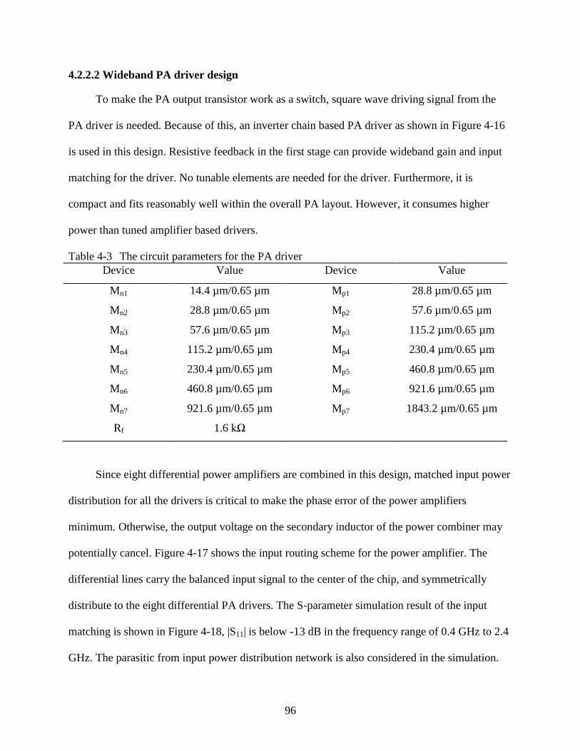
96
4.2.2.2 Wideband PA driver design
To make the PA output transistor work as a switch, square wave driving signal from the
PA driver is needed. Because of this, an inverter chain based PA driver as shown in Figure 4-16
is used in this design. Resistive feedback in the first stage can provide wideband gain and input
matching for the driver. No tunable elements are needed for the driver. Furthermore, it is
compact and fits reasonably well within the overall PA layout. However, it consumes higher
power than tuned amplifier based drivers.
Table 4-3 The circuit parameters for the PA driver
Device Value Device Value
Mn1 14.4 µm/0.65 µm Mp1 28.8 µm/0.65 µm
Mn2 28.8 µm/0.65 µm Mp2 57.6 µm/0.65 µm
Mn3 57.6 µm/0.65 µm Mp3 115.2 µm/0.65 µm
Mn4 115.2 µm/0.65 µm Mp4 230.4 µm/0.65 µm
Mn5 230.4 µm/0.65 µm Mp5 460.8 µm/0.65 µm
Mn6 460.8 µm/0.65 µm Mp6 921.6 µm/0.65 µm
Mn7 921.6 µm/0.65 µm Mp7 1843.2 µm/0.65 µm
Rf 1.6 kΩ
Since eight differential power amplifiers are combined in this design, matched input power
distribution for all the drivers is critical to make the phase error of the power amplifiers
minimum. Otherwise, the output voltage on the secondary inductor of the power combiner may
potentially cancel. Figure 4-17 shows the input routing scheme for the power amplifier. The
differential lines carry the balanced input signal to the center of the chip, and symmetrically
distribute to the eight differential PA drivers. The S-parameter simulation result of the input
matching is shown in Figure 4-18, |S11| is below -13 dB in the frequency range of 0.4 GHz to 2.4
GHz. The parasitic from input power distribution network is also considered in the simulation.

97
RFin+ RFin-
PA Driver
Figure 4-17. Input power distribution scheme for the power amplifier.
0.4 0.8 1.2 1.6 2.0 2.4-18
-17
-16
-15
-14
-13
-12
-11
-10
|S11|
(dB
)
Frequency (GHz)
Figure 4-18. Simulated |S11| for the input matching of the driver.

98
4.2.2.3 Transformer based power combiner design
Figure 4-19 shows the slab inductor based transformer with a patterned ground shield used
for each power amplifier [63], [64]. The secondary inductor is stacked vertically above the
primary inductor. The current through the primary inductor of the transformer is larger than the
current in the secondary inductor. Therefore, a thicker metal is used for the primary inductor.
The thicknesses of metal-6 and Al-cap layer are ~1.6 μm and ~1 μm, respectively. The inter-
layer dielectric thickness is ~0.85 μm. Perpendicular metal-1 patterned ground shield is used to
steal the electrical field from the substrate. Ideally, the influence on the magnetic field is small
since the slots in the shield avoid the generation of induced currents. To further prevent substrate
loss, high resistivity layer (HiRES) is used to cover the substrate area underneath the
transformer. The HiRES layer blocks the p-well doping and makes the substrate less conductive.
Alcap
Cut the magnetic
induced current
Metal 1
(ground shield)
Metal 6
Figure 4-19. 3-D view of the stacked transformer with patterned ground shield.
The conductor width and length of the stacked transformer are chosen as 60 μm and 960
μm. A compact model in Figure 4-20 [76], [78], [79], [80] is used to fit the simulation results
from the EM simulator. Capacitance Cp and Cs are shunted with the primary and secondary

99
inductor, respectively to frequency tune the transformer. 6.25 Ω S-parameter simulation results
of the transformer in both low frequency and high frequency bands are shown in Figure 4-21.
2Cp1
Rsub1/2
Cp1
Rsub1
Cp1
Rsub1
Cp2
Rsub2
Cp2
Rsub2
2Cp2
Rsub2/2
2CcCc Cc
Rpf
Lpf
Lsf
Rsf
Rp Lp
Rs Ls
RpLp
RsLs
Rpf
Lpf
Lsf
Rsf
P1
P3
P2
P4
k k
Figure 4-20. Compact model for the stacked transformer.
Table 4-4 The extracted equivalent circuit parameters for the 1:1 slab inductor based
transformer, interconnection parasitic are also included in the simulation
Circuit parameters Extracted value Circuit parameters Extracted value
Lp 0.7nH Ls 0.8nH
Rp 0.28 Rs 0.59
Lpf 0.08nH Lsf 0.13nH
Rsf 0.003Ω Rpf 0.006Ω
Cp1 140fF Rsub1 15Ω
Cp2 12fF Rsub2 5kΩ
Cc 650fF k 0.85

100
0.4 0.8 1.2 1.6 2.0 2.4-10
-9
-8
-7
-6
-5
-4
-3
-2
-1
0
Low Frequency Band
|S21|
(dB
)
Frequency (GHz)
High Frequency Band
Figure 4-21. Transformer S-parameter (|S21|) simulation in both low frequency and high
frequency bands.
VPA7+
Alcap
Metal 6
VDD1
OUT+
OUT-
VPA1+ VPA1-
VDD2
VPA2+
VPA2-
VDD3
VDD4
VDD5
VDD6
VDD7
VDD8
VPA3+
VPA3-
VPA4-
VPA4+
VPA5- VPA5+
VPA6-
VPA6+
VPA7-
VPA8-
VPA8+
A
VPA+ VPA-VDD
B
Figure 4-22. Conceptual drawing of the power combiner.

101
The conceptual drawing of power combiner with eight transformers is shown in Figure 4-
22. The primary side of each transformer is connected to a differential power amplifier and the
secondary sides of all the transformers are connected in series to combine the output AC voltage.
DC supply voltage VDD is fed into the center of primary inductor of each transformer.
4.2.2.4 Multiband tuning circuits design
VPA+ VPA-VDD
Cp/2
A
VPA+ VPA-VDD
CpCp
B
Figure 4-23. The tuning capacitor connection at the primary inductor, A) differential connection
across the two nodes of the primary inductor, B) separate single-ended connection
from the two nodes to ground.
As mentioned in section 4.2.1, series connection of L2 and C2 is used as a second order
harmonic short of the power amplifier. At the fundamental frequency, the series connection is
capacitive. This equivalent capacitance along with the parasitic drain capacitance Cout is used as
part of the transformer tuning capacitance Cp. It is not practical to connect the tuning capacitor
Cp across VPA+ and VPA- of the primary inductor because the parasitic inductance of the capacitor

102
routing becomes comparable with the inductance of the primary inductor as shown in Figure 4-
23 (A) [63], [64], [66]. Tuning capacitors between drain and ground are used instead as shown in
Figure 4-23 (B). This however increases the required capacitance.
Once the dimension of transformer power combiner is decided, tuning capacitance at the
primary side of each transformer will be decided as CpH and CpL for higher and lower bands
respectively. The capacitance values of C2 for higher (C2H) and lower (C2L) band are:
2 2
2
1
4H
H
CL
(4-9)
2 2
2
1
4L
L
CL
.
(4-10)
ωH and ωL are the center frequencies for higher and lower bands. L2 of 350 pH is chosen in this
design. At the fundamental frequency, the equivalent capacitances of the series connection of L2
and C2 are
, 2
2
1
3eq H
H
CL
(4-11)
, 2
2
1
3eq L
L
CL
(4-12)
Therefore, the shunt capacitances of C1 at higher and lower band are shown as below
1 ,H pH out eq HC C C C
(4-13)
1 ,L pL out eq LC C C C
(4-14)
Figure 4-24 shows the schematic of watt level multi-band power amplifier with tunable
capacitors. The tunable capacitor banks C1 and C2 are realized by using a binary array of metal
capacitors on top of switches, as shown in Figure 4-25. In each tuning bank, there are four
voltage controls. Take the switch capacitor CM and M1 for example, when the control voltage is
―1‖, the transistor will be turned on and the capacitance is CM. And when the control voltage is
―0‖, the total capacitance value is equal to CM(Cd+CM,p)/(CM+Cd+CM,p). To increase the tuning
range of the capacitor bank, a minimum length transistor is used and transistor width should be

103
small to reduce the parasitic drain capacitance. However, small transistor size will degrade the Q
of capacitor bank since the turn on resistance would be increased. Quality factors of C1 and C2
were swept separately to check the impact of capacitor tuning bank Q on the performance of the
power amplifier.
Cout
VDD_PA
M1 M2
C2
L2
Lp/2
RFout
RFin+ RFin-
Cs
C1
Figure 4-24. Multiband power amplifier with tunable switch capacitor banks.
Figure 4-26 shows the simulated plot of power amplifier drain efficiency versus the Q of
C1 and C2 at 900MHz band. The transistor and transformer loses are also considered in the

104
simulation. Q of each capacitor bank is swept separately while the other capacitor bank is
assumed to be ideal. The drain efficiency versus Q of C1 and C2 at 1700 MHz band is shown in
Figure 4-27. Tuning bank Q of larger than 15 and 20 in lower band and higher band are chosen
to meet the tuning range while not significantly degrading the drain efficiency.
CM
W/L
Cd
Vc1
M1
2W/L
2Cd
Vc2
M2
CM,p 2CM,p
4W/L
4Cd
M3
4CM,p
8W/L
8Cd
M4
8CM,p
2CM 4CM 8CM
Vc3 Vc4
Figure 4-25. Multiband power amplifier with tunable switch capacitor banks.
0 5 10 15 20 25 30 35 40
26
28
30
32
34
36
38
40
C1
C2
Dra
in e
ffic
ien
cy (
%)
Capacitor Q
Figure 4-26. Drain efficiency of the PA versus the Q of the capacitor tuning bank C1 and C2 at
lower frequency band (850 MHz).

105
0 5 10 15 20 25 30 35 40
27
30
33
36
39
42
45
48
C1
C2
Dra
in E
ffic
ien
cy (
%)
Capacitor Q
Figure 4-27. Drain efficiency of the PA versus the Q of the capacitor tuning bank C1 and C2 at
higher frequency band (1700 MHz).
4.2.2.5 Bypassing of the multiband power amplifier
Power amplifiers at low supply voltage, requires larger current from the DC voltage
supply. On-chip and PCB bypassing are critical to make the power amplifier properly work. For
differential amplifiers, the drain current is symmetrical and the current through the supply bond
wires is approximately DC. But this is the ideal case and only valid when the differential
amplifier is driven by small signal. In this design, the PA output stage is overdriven and working
as a switch. Therefore, in general the drain current is not symmetric and there is AC current from
the supply. Furthermore, the supply and ground bond wires between the chip and PCB introduce
finite inductance LVDD_bond and LGND_bond as shown in Figure 4-28. Those inductors will cause
ground bounce. To suppress the AC current ripple through the VDD of each differential power

106
amplifier, 300 pF on-chip MOS capacitors are placed close to the DC feed point of each
transformer. 3 pF capacitance cells are shunted together to form the capacitors.
IN+ IN-
GNDchip LGND_bond
LVDD,para
OUT+ OUT-
LGND,para
IT
I1 I2 LVDD_bond
Cchip,decoup
Rchip,decoup
GNDchip
To PCB
Figure 4-28. Differential amplifier with parasitic inductances from the routing and bond wires.
Compared to on-chip bypassing, printed circuit board (PCB) bypassing is more
complicated because of the frequency limitation of the off-chip capacitors. The bypass scheme
on PCB is shown in Figure 4-29. Bulk capacitors (usually Tantalum capacitors) are used to
stabilize the supply voltage on a PCB at low frequency and the purpose of high frequency
capacitors (usually ceramic capacitors) is to reject the high frequency ripple on the supply. A
combination of the capacitors is to properly AC ―ground‖ the PCB supply at the frequency range
of interests. In the equivalent circuit model of the capacitor as shown in Figure 4-29, equivalent
series resistor (ESR) and series inductor (ESL) model the DC and frequency dependent losses of
the capacitor. The parasitic inductance of package makes the off chip capacitor inductive when
the frequency is higher than the self resonant frequency (SRF) of capacitor. We can use multiple
capacitors with varies SRF to realize the low impedance bypassing at the frequency range of

107
interests. The inductance of metal traces on a PCB should be also considered since it changes the
SRF of capacitor.
Wire connection
Power
supply
Bulk
capacitor
To Chip
High frequency
capacitor
C
Rleak
ESL ESR
On PCB
Figure 4-29. Printed circuit board bypassing for power amplifier performance evaluation.
4.2.3 Measurement Results
The multiband PA is fabricated in 1.2 V TI 65 nm CMOS technology. The test chip is
mounted on a PCB to evaluate its performance. The power measurement setup is shown in
Figure 4-30. Due to the high supply current for the PA output stage, three separate DC supplies
are used. The DC feed points of the eight differential power amplifiers are bonded out to three
separate DC pads on PCB as shown in Figure 4-31. The balanced 50 Ω load is provided by
connecting each output node of the on-chip power combiner to a 25 Ω load consisting two
parallel 50 Ω terminators.

108
PA
Ex
te
rn
al
Ba
lu
n
50Ω
RFout
Signal generator
External PA
RFin
DUT
DC power supply
Spectrum Analyzer
Figure 4-30. Power amplifier power measurement setup.
Figure 4-32 shows a photograph of printed circuit board for the test chip performance
evaluation. An off-chip balun is used to generate the differential input signal for the PA driver.
External RF chocks are also connected to the supply on the printed circuit board to avoid the
unexpected oscillation. The chip on board bonding diagram and the PA die photo are shown in
Figure 4-33. To reduce the ground bond-wire inductance, two rings of bond pads are used to
improve ground connection. The dimension of the chip is about 3.5 mm x 3.5 mm including the
bond pads. The chip is mounted on the ground pad of printed circuit board using electronically
and thermally conductive epoxy to further reduce the ground inductance and to help heat
dissipation. A heat sink is also attached to the back of the printed circuit board. The tuning of
secondary inductor for the power combiner is realized by using an external trimmer. All power
losses from the setup are de-embedded. The power loss of the bond wire is included in the PA
measurement results.

109
OUT+
50Ω 50Ω
50Ω50Ω
OUT-
Test Chip
VDD on PCB
Bond wire
Cs
Figure 4-31. Separate VDD on printed circuit board for PA evaluation.
Differential input
Driver VDDDriver VDD
PA VDD
PA VDD
Test Chip
Differential output
Figure 4-32. Photograph of the printed circuit board for chip evaluation.

110
VDD_Drv2
VDD_Drv1
VDD_Drv3
VDD_Drv4
VDD_PA1
VDD_PA2
VDD_PA3
GND
OUT+ OUT-
IN+ IN-
VC1_1
VC1_2
VC1_3
VC1_4
VC2_1
VC2_2
VC2_3
VC2_4
Bypass cap
L2
C2
C1
A differential
PA
Figure 4-33. Chip on board bonding scheme and the die photo of multi-band power amplifier.

111
Figure 4-34 shows the measured output power, drain efficiency and power added
efficiency of the multi-band PA working at the lower band (850 MHz). The supply voltage
VDD_Drv for the square wave driver of 1.8 V is used to overdrive the PA stage. The supply voltage
of PA stage VDD_PA during the frequency sweep measurement is kept at 1.2 V. The PA is tuned at
850 MHz with 30.2 dBm saturated output power with drain efficiency and power added
efficiency of 24.3% and 20.6%, respectively. The measured output power, drain efficiency and
power added efficiency versus PA stage DC supply VDD_PA at 850 MHz are plotted in Figure 4-
35. Output power versus input power characteristic of the PA at 850 MHz is shown in Figure 4-
36. The PA output power is saturated when the input power is larger than 15.2 dBm with power
gain of 15 dB.
800 850 900 950 100025
26
27
28
29
30
31
PAE
Frequency (MHz)
Ou
tpu
t P
ow
er
(dB
m)
Drain efficiency
12
15
18
21
24
27
30
Effic
ien
cy (%
)
Figure 4-34. Measured output power, drain efficiency and power added efficiency of the multi-
band PA versus frequency at the lower band.

112
0.8 0.9 1.0 1.1 1.2 1.3 1.426
27
28
29
30
31
Vdd_PA (V)
Ou
tpu
t P
ow
er
(dB
m)
10
15
20
25
30
35
PAE
Effic
ien
cy (%
)
Drain efficiency
Figure 4-35. Measured output power, drain efficiency and power added efficiency versus PA
stage DC supply VDD_PA at 850 MHz.
4 6 8 10 12 14 16 1815
18
21
24
27
30
PAE
Drain Efficiency
Input Power (dBm)
Ou
tpu
t P
ow
er
(dB
m)
0
5
10
15
20
25
30
35
Effic
ien
cy (%
)
Figure 4-36. Measured output power versus input power characteristics of the PA at 850 MHz.

113
Figure 4-37 shows the measured output power, drain efficiency and power added
efficiency of the PA in the higher band. The supply voltage VDD_Drv for the square wave driver is
once again 1.8 V and the supply voltage of the PA stage VDD_PA is 1.2 V. The PA is tuned at
1700 MHz achieving 29.5 dBm saturated output power with drain efficiency and power added
efficiency of 22.2% and 16.7% respectively. The measured output power, drain efficiency and
power added efficiency versus PA stage DC supply VDD_PA at 1700 MHz is plotted in Figure 4-
38. The output power versus input power characteristics of PA at 1700 MHz are shown in Figure
4-39. The PA output power is saturated when the input power is larger than 17.4 dBm with
saturated power gain of 12.5 dB.
1.5 1.6 1.7 1.8 1.922
24
26
28
30
Frequency (GHz)
Ou
tpu
t P
ow
er
(dB
m)
12
15
18
21
24
PAE
Effic
ien
cy (%
)
Drain Efficiency
Figure 4-37. Measured output power, drain efficiency and power added efficiency of the multi-
band PA versus frequency at the higher band.

114
0.9 1.0 1.1 1.2 1.3 1.4 1.525
26
27
28
29
30
31
PAE
Vdd_PA (V)
Ou
tpu
t P
ow
er
(dB
m)
Drain Efficiency
12
15
18
21
24
27
30
Effic
ien
cy (%
)
Figure 4-38. Measured output power, drain efficiency and power added efficiency versus PA
stage DC supply VDD_PA at 1700 MHz.
6 8 10 12 14 16 18 2015
18
21
24
27
30
Drain Efficiency
PAE
Input Power (dBm)
Ou
tpu
t P
ow
er
(dB
m)
0
5
10
15
20
25
30
Effic
ien
cy (%
)
Figure 4-39. Measured output power versus input power characteristics of the PA working at
1700 MHz.

115
The performance of multi-band tunable watt-level power amplifier is summarized in Table
4-5. Table 4-6 shows the performance comparisons with the tunable power amplifier
performance in the literature. The performance comparisons with the power amplifiers in nano-
scale CMOS technology are listed in Table 4-7.
Table 4-5 Summary of the measured multi-band power amplifier performance
Frequency Band Lower band (850 MHz) Higher band (1700 MHz)
Driver VDD 1.8V 1.8V
PA stage VDD 1.2V 1.2V
Driver DC current 0.38A 0.8A
PA stage Current 3.6A 3.8A
Output power 30.2 dBm 29.5 dBm
Drain efficiency 24.3% 22.2%
Power added efficiency 20.6% 16.7%
Saturated power gain 15 dB 12.5 dB
Table 4-6 Performance comparison to the previously published tunable multi-band CMOS
power amplifiers
Reference [71] [74] [75] This Work
Frequency (GHz) 1.9/2.3/2.6/3.5 2.45/3.8 0.9~3 0.85/1.7
Technology 0.18 µm 0.18 µm 0.18 µm 65nm
VDD (V) 3.3 3.3 3.3 1.2
Psat (dBm) 24.2/23.8/23.4/20.5 23.4/24.5 20~21 30.2/29.5
Peak Drain Efficiency (%) 48.2/44.3/40.9/35.6 42/39 24.3/22.2
Peak PAE (%) - - 11~23 20.6/16.7
Chip Area (mm2) 1.61 1 0.31 12.25

116
Table 4-7 Performance comparison to the previously published power amplifiers in nano-scale
CMOS
Frequency
(GHz)
CMOS
Technology
VDD
(V)
Transistor
Type
Psat
(dBm)
Peak PAE
(%)
Chip Area
(mm2)
Ref.
2.4 65 nm 1 TN 21.8 44 - [82]
1.8 65 nm 3.4 TN/TK 29.4 51 - [83]
2.5 0.18 µm 3.3 TN/TK 31 34.8 1.98 [84]
2.75 32 nm 1.8 TN/TK 28 31.9 2 [85]
2.4 32 nm 2 TN 25.3 35 1.28 [86]
2.4 65 nm 3.3 TN/TK 31.5 25 2.7 [87]
2.4 90 nm 3.3 TN/TK 30.1 33 4.2 [88]
2.5 90 nm 3.3 TN/TK 32 48 2.25 [89]
2 0.13 µm 3.3 TN/TK 29.3 69 4 [90]
1.8 0.18 µm 3.3 TN/TK 31.2 41% 2.2 [65]
0.85/1.7 65 nm 1.2 TN 30.2/29.5 20.6/16.7 12.25
This
work
TN: Thin gate-oxide transistor, TK: Thick gate-oxide transistor.
4.3 Conclusions
A tunable multi-band power amplifier designed in 1.2 V TI 65 nm CMOS process is
presented in this chapter. It utilizes an on-chip transformer based power combiner where eight
differential PAs are combined in order to achieve watt-level output power. A tapered inverter
driver with resistive feedback is designed to provide wideband input matching and square wave
drive for the PA stage. Capacitor tuning banks are used to realize the frequency tuning between
850 MHz and 1700 MHz. At 850 MHz band, the saturated output power of 30.2 dBm with drain
efficiency and power added efficiency of 24.3% and 20.6% is achieved. It has saturated power

117
gain of 15 dB. At 1700 MHz, the saturated output power is 29.5 dBm with 12.5 dB gain. Drain
efficiency and power added efficiency are 22.2% and 16.7%. This is the first tunable multi-band
watt-level power amplifier using nano-scale CMOS technology that supports 850 MHz and 1700
MHz frequency bands with supply voltage lower than 2 V.

118
CHAPTER 5
SUMMARY AND FUTURE WORK
5.1 Summary
A T/R switch and a power amplifier are two high power RF transceiver building blocks.
They are also the barriers for realizing a single CMOS radio. The research work in this
dissertation suggests possible approaches and provides understanding of limitations for
implementing T/R switches with high power handling capability and frequency tunable power
amplifiers with high output power in advanced CMOS technologies.
Compared to MOS transistors in nano-scale CMOS, p-n diodes have the advantage of high
breakdown voltage. The possibility of using an on chip p-n diode to implement a broadband
NMOS/Diode hybrid CMOS T/R switch has been evaluated. Only thin-gate-oxide transistors
along with a p-n diode are used. Transmit and receive insertion loss of 0.5dB and 1.1 dB, and
IP1dB of ~28 dBm have been achieved in a 45 nm bulk CMOS process using a series NMOS and
series diode hybrid configuration. This is the first effort to evaluate the performance, in particular
the power handling capability can be achieved for a T/R switch operating around 900 MHz using
p-n diodes in nano-scale CMOS.
A fully integrated 2.4 GHz CMOS Class-F power amplifier in UMC 130 nm single poly-
silicon and eight metal layer digital CMOS process is demonstrated. The single-ended power
amplifier consists of a tapered inverter driver with wideband resistive feedback input matching
and an output stage with a fully integrated third harmonic peaking network incorporating
impedance transformation. The drain efficiency and PAE are 46.5% and 38%, respectively at 1.2
V supply voltage. The saturated output power is 12.4 dBm with 13.9 dB power gain. The 2.4
GHz operation frequency is the lowest at which full integration of Class-F PA in CMOS is
demonstrated.

119
A tunable multi-band power amplifier fabricated in the 1.2 V TI 65 nm CMOS process is
presented. It has an on-chip transformer based power combiner where eight differential PAs are
combined in order to achieve watt-level output power. A tapered inverter driver with resistive
feedback is designed to provide wideband input matching. Capacitor tuning banks are used to
realize the multi-band tuning at 850 MHz and 1700 MHz. At 850 MHz, the saturated output
power of 30.2 dBm with drain efficiency and power added efficiency of 24.3% and 20.6% is
achieved when the driver and PA stage supply voltage of 1.8 V and 1.2 V, respectively. At 1700
MHz, the saturated output power is 29.5 dBm with 12.5 dB gain. Drain efficiency and power
added efficiency of 22.2% and 16.7% are achieved under the driver and PA stage supply voltage
of 1.8 V and 1.2 V, respectively. This is the first tunable multi-band watt-level power amplifier
using nano-scale CMOS technology that supports 850 MHz and 1700 MHz frequency bands
with supply voltage lower than 2 V.
5.2 Future Work
The following future work that extends the effort described in this dissertation is
suggested. As mentioned in chapter 2. The NMOS/Diode hybrid T/R switch requires DC power
consumption in RX mode, and approaches to lower this including further reduction of current
gain of parasitic p-n-p transistors should be considered. A Schottky diode is another type of
diodes available in standard foundry CMOS process. When a Schottky diode is forward biased,
the parasitic vertical p-n-p transistor action as shown in Figure 2-24 is avoided. The turn on
voltage of Schottky diode is also smaller compared to p-n diodes. This should lower the power
consumption and make Schottky diodes a better choice for implementing diode T/R switch in
CMOS technology. The schematic of T/R switch using a Schottky diode is shown in Figure 5-1.
Evaluation of this prototype is suggested in the future.

120
TX
ANTVG1
Rsub
VB
M1
D1 RX
Q1
L1
L2
VG2
M2
Vbias3
CB1
CB2
CB3
Vbias1 Vbias2
P N
P1
N1
Off-chip component
Bond-pad
M3
VDD
VG3
Figure 5-1. Schematic of NMOS/Diode hybrid T/R switch using a Schottky diode.
A tunable multi-band watt-level power amplifier is demonstrated in chapter 4. Mechanical
trimmer is used at the PA output to turn the secondary inductor of the transformer based power
combiner. A tuning method using voltage controlled variable capacitor is suggested in Figure 5-
2. Since the voltage swing at the output of the power combiner is large, MOS capacitor based
varactors cannot be used here due to their low breakdown voltage. On-chip diode or external PIN
diode [92] based varactors could be considered. For on-chip diode based varactor option, high
breakdown voltage diode is needed. N-well to p-substrate diode has the largest breakdown
voltage among the diodes available in standard CMOS technology because of the lower doping
density for n-well. On the other hand, series resistance of such diode is relatively high and will
degrade the Q of the varactor. Therefore, multiple diode cells should be shunted in parallel.

121
VPA7+
VDD1
OUT+
OUT-
VPA1+ VPA1-
VDD2
VPA2+
VPA2-
VDD3
VDD4
VDD5
VDD6
VDD7
VDD8
VPA3+
VPA3-
VPA4-
VPA4+
VPA5- VPA5+
VPA6-
VPA6+
VPA7-
VPA8-
VPA8+
Vc
Figure 5-2. Voltage-controlled tuning at the output of power combiner.

122
APPENDIX
PRINTED CIRCUIT BOARD DESIGN FOR MULTI-BAND PA EVALUATION
As mentioned in chapter 4, printed circuit board is important for low voltage and high
current PA evaluation. Four-layer printed circuit board is used in the multi-band watt-level
power amplifier measurement in order to use the layer-to-layer capacitance with high self
resonant frequency. The layer thicknesses are shown in Figure A-1. Figure A-2 shows the layout
of top layer. The DC supply for PA output stage is divided into three separate sections to reduce
the current flowing through each supply plane. The main routings on the top layer is ground
plane and PA stage supply plane. To increase the printed circuit board capacitance for
bypassing, the second layer is chosen as ground plane. The layout of second layer is shown in
Figure A-3. For layer 3, it is mainly power plane which is divided into three power sections for
power amplifier output stage, and four power plans for driver as shown in Figure A-4. The
current through driver stage is not high and the bypassing requirement is not demanding. Having
four driver power sections is only for ease of interconnection. Figure A-5 shows the layout of
bottom plane, which is mainly composed of a ground plane. Four symmetric outputs are also
routed on the bottom plane of the PCB.
Top (copper 0.035 mm)
Dialectric (0.18 mm)
L2 (copper 0.07 mm)
Dialectric (1 mm)
L3 (copper 0.07 mm)
Bottom (copper 0.035 mm)
Dialectric (0.18 mm)
Figure A-1. Four-layer printed circuit board thicknesses.
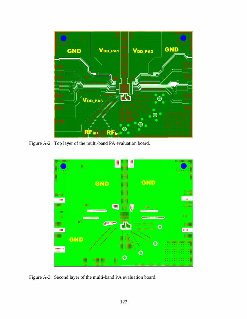
123
VDD_PA1 VDD_PA2
VDD_PA3
RFin+ RFin-
GNDGND
Figure A-2. Top layer of the multi-band PA evaluation board.
GND GND
GND
Figure A-3. Second layer of the multi-band PA evaluation board.

124
VDD_PA1 VDD_PA2
VDD_PA3
VDD_Drv1
VDD_Drv2
VDD_Drv3
VDD_Drv4
GND
Figure A-4. Third layer of the multi-band PA evaluation board.
GND
Out+
Out-
Figure A-5. Bottom layer of the multi-band PA evaluation board.

125
LIST OF REFERENCES
[1] T. H. Lee, The Design of CMOS Radio Frequency Integrated Circuits, Second Edition.
Cambridge, U.K, Cambridge University Press, 2004.
[2] Q. Gu, RF System Design of Transceivers for Wireless Communications, Springer, 2005.
[3] B. Razavi, Design of Analog CMOS Integrated Circuits, McGraw Hill, 2001.
[4] X. L, Y. Zhang, ―Flipping the CMOS Switch‖, IEEE Microwave Magazine, pp. 86-96,
February. 2010.
[5] K. H. An, ―CMOS power amplifiers for mobile wireless communications,‖ Ph.D.
dissertation, Department of Electrical and Computer Engineering, Georgia Institute of
Technology, Atlanta, GA, 2009.
[6] Naratip Wongkomet, ―Efficiency Enhancement Techniques for CMOS RF Power
Amplifiers‖, Ph.D. dissertation, Department of Electrical Engineering and Computer
Science, University of California at Berkeley, CA, 2006.
[7] W. C. Edmund Neo, Yu Lin, Xiao-dong Liu, Leo C. N. de Vreede, Lawrence E. Larson,
Marco Spirito, Marco J. Pelk, Koen Buisman, Atef Akhnoukh, Anton de Graauw, and Lis
K. Nanver, ―Adaptive Multi-Band Multi-Mode Power Amplifier Using Integrated
Varactor-Based Tunable Matching Networks‖, IEEE Journal of Solid State Circuits, vol.
41, no. 9, September 2006.
[8] Z. Li, Radio Frequency Circuits for Tunable Multi-Band CMOS Receivers for Wireless
LAN Applications, Ph. D. Dissertation, University of Florida, Gainesville, FL, 2004.
[9] S. Yim and K. K. O, ―Demonstration of a switched resonator concept in a dual-band
monolithic CMOS LC-tuned VCO,‖ in Proc. IEEE Custom Integrated Circuits Conf.,
San Diego, CA, pp 205-208, May 2001.
[10] Z. Li, R. Quintal, and K. K. O, ―A dual-band CMOS front-end with two gain modes for
wireless LAN applications,‖ IEEE J. Solid-State Circuits, vol. 39, no. 11, pp. 2069–2073,
Nov. 2004.
[11] Z. Li, K. K. O, ―A Low-Phase-Noise and Low-Power Multiband CMOS Voltage-
Controlled Oscillator‖, IEEE J. Solid-State Circuits, vol. 40, no. 6, pp. 1296–1302, June.
2005.
[12] J. Ryynanen, K. Kivekas, J. Jussila, A. Parssinen, and K. Halonen, ―A dual-band RF
front-end for WCDMA and GSM applications,‖ in Proc. IEEE Custom Integrated
Circuits Conf., 2000, pp. 175–178.
[13] Kaczman, D, Shah, M.; Alam, M.; Rachedine, M.; Cashen, D.; Lu Han; Raghavan, A, ―A
Single–Chip 10-Band WCDMA/HSDPA 4-Band GSM/EDGE SAWless CMOS Receiver

126
With DigRF 3G Interface and +90 dBm IIP2‖, IEEE J. Solid-State Circuits, vol. 44, no.
3, pp. 718–739, March. 2009.
[14] Bakkaloglu, B.; Fontaine, P.; Mohieldin, A.N.; Solti Peng; Sher Jiun Fang; Dulger, F, ―A
1.5-V multi-mode quad-band RF receiver for GSM/EDGE/CDMA2K in 90-nm digital
CMOS process‖, IEEE J. Solid-State Circuits, vol. 41, no. 5, pp. 1149–1159, May. 2006.
[15] H. Xu, Investigation of Thick-Gate-Oxide MOS Structures With Sub-Design-Rule
Channel Lengths for Digital and Radio Frequency Circuits Applications, Ph. D.
Dissertation, University of Florida, Gainesville, FL, 2007.
[16] F. –J. Huang and K. K. O, ―A 0.5 µm CMOS T/R Switch for 900 MHz Wireless
Applications,‖ IEEE J. Solid-State Circuits, vol. 36, pp. 486-492, Mar. 2001.
[17] F. –J. Huang and K. K. O, ―A 2.4 GHz Single-Pole Double-Throw T/R Switch with 0.8
dB Insertion-Loss Implemented in a CMOS Process,‖ Proc. 27th
Eur. Solid-State Circuits
Conf., pp. 432-435, 2001.
[18] F. –J. Huang, Schottky Clamped MOS Transistors for Wireless CMOS Radio Frequency
Switch Applications, Ph. D. Dissertation, University of Florida, Gainesville, FL, 2001.
[19] Z. Li and K. K. O, ―15-GHz Fully Integrated NMOS Switches in A 0.13-µm CMOS
Process,‖ IEEE Journal of Solid-State Circuits, vol. 40, no. 11, pp. 2323-2328, Nov. 2005.
[20] Z. Li, H. Yoon, F. –J. Huang, and K. K. O, ―5.8-GHz CMOS T/R Switches with High
and Low Substrate Resistance in a 0.18-µm CMOS Process,‖ IEEE Microwave and
Wireless Component Letters, vol. 13, no. 1, pp. 1-3, Jan. 2003.
[21] Mei-Chao Yeh et al., ―A Miniature Low-Insertion-Loss, High-Power CMOS SPDT
Switch Using Floating-Body Technique for 2.4- and 5.8-GHz Applications,‖ IEEE RFIC
Symp. Dig., pp. 451-454, 2005.
[22] Mei-Chao Yeh, Zuo-Min Tsai, Ren-Chieh Liu, Kun-You Lin, Ying-Tang Chang, and
Huei Wang, ―Design and Analysis for a Miniature CMOS SPDT Switch Using Body-
Floating Technique to Improve Power Performance‖, IEEE Transactions on Microwave
Theory and Techniques, vol. 54, no. 1, pp. 31-39, January. 2006.
[23] T. Ohnakado, et al, ―A 0.8-dB Insertion-Loss, 17.4-dBm Power-Handling, 5-GHz
Transmit/Receive Switch With DETs in a 0.18-µm CMOS Process,‖ IEEE Electron
Device Letters, vol. 24, no. 3, pp. 192-194, Mar. 2003.
[24] T. Ohnakado, S. Yamoakawa, T. Murakami, A. Furukawa, E. Taniguchi, H. Ueda, N.
Suematsu and T. Oomori, ―21.5-dBm Power-Handling 5-GHz Transmit/Receive CMOS
Switch Realized by Voltage Division Effect of Stacked Transistor Configuration With
Depletion-Layer-Extended Transistors (DETs),‖ IEEE J. of Solid-State Circuits, vol. 39,
no. 4, pp. 577-584, Apr. 2004.

127
[25] N. A. Talwalkar, C. P. Yue, H. Gan and S. S. Wong, ―Integrated CMOS transmit-receive
switch using LC-tuned substrate bias for 2.4-GHz and 5.2-GHz applications,‖ IEEE J.
Solid-State Circuits, vol. 39, no. 6, pp. 863-870, Jun. 2004.
[26] H. Xu and K. K. O, ―A 31.3-dBm Bulk CMOS T/R Switch Using Stacked Transistors
With Sub-Design-Rule Channel Length in Floated p-wells,‖ IEEE Journal of Solid-State
Circuits, vol. 42, no. 11, pp. 2528-2534, Nov. 2007.
[27] Minsik Ahn, Chang-Ho Lee, Byung Sung Kim, and Joy Laskar, ―A High-Power CMOS
Switch Using A Novel Adaptive Voltage Swing Distribution Method in Multistack
FETs‖, IEEE Transactions on Microwave Theory and Techniques, vol. 56, no. 4, pp. 849-
858, April. 2008.
[28] C. –T Fu, S. S. Taylor, and C. –N. Kuo, ―A 5-GHz, 30-dBm, 0.9-dB Insertion Loss
Single-Pole Double-Throw T/R Switch in 90nm CMOS,‖ 2008 IEEE Radio Frequency
Integrated Circuits Symposium, pp. 317-320, Jun. 2008.
[29] Minsik Ahn, Hyun-Woong Kim, Chang-Ho Lee, and Joy Laskar, ―A 1.8-GHz 33-dBm
P0.1-dB CMOS T/R Switch Using Stacked FETs With Feed-Forward Capacitors in a
Floated Well Structure‖, IEEE Transactions on Microwave Theory and Techniques, vol.
57, no. 11, pp. 2661-2670, November. 2009.
[30] A. A. Kidwai, C-T. Fu, J. C. Jensen, S. S. Taylor, ―A Fully Integrated Ultra-Low
Insertion Loss T/R Switch for 802.11b/g/n Application in 90 nm CMOS Process,‖ IEEE
Journal of Solid-State Circuits, vol. 44, no. 5, pp. 1352-1360, May. 2009.
[31] C.–T Fu, H. Lakdawala, S. S. Taylor, and K. Soumyanath, ―A 2.5GHz 32nm 0.35mm2
3.5dB NF -5dBm P1dB Fully Differential CMOS Push-Pull LNA with Integrated 34dBm
T/R Switch and ESD Protection,‖ ISSCC Dig. Tech. Papers, pp. 56-58, Feb. 2011.
[32] S. Sankaran, Receivers Using Schottky Barrier Diodes in CMOS, Ph. D. dissertation,
University of Florida, 2008.
[33] P. R. Gray, P. J. Hurst, S. H. Lewis, R. G. Meyer, Analysis and Design of Analog
Integrated Circuits, 4th ed. New York: Wiley, 2001.
[34] S. C. Cripps, RF Power Amplifiers for Wireless Communication, Artech House, 1999.
[35] P. Reynaert, RF Power Amplifiers for Mobile Communications, Springer, 2006.
[36] Scott. Kee, The Class E/F Family of Harmonic Tuned Switching Power Amplifiers, Ph.
D dissertation, California Institute of Technology, 2002
[37] N. O. Sokal and A. D. Sokal, ―Class E –A New Class of High-Efficiency Tuned Single-
Ended Switching Power Amplifiers‖, IEEE Journal of Solid State Circuits, vol. sc10,
no.3, pp. 168-176, June 1975.

128
[38] N. O. Sokal and F. H. Raab, ―Harmonic output of class-E RF power amplifiers and load
coupling network design,‖ IEEE J. Solid-State Cir- cuits, vol. 12, no. 1, pp. 86–88, Feb.
1977.
[39] N. O. Sokal, ―Class-E power amplifiers,‖ QEX/Communications Quarterly, pp. 9–20,
2001.
[40] R. Brama et al., ―A 30.5 dBm 48% PAE CMOS class-E PA with integrated balun for RF
applications,‖ IEEE J. Solid-State Circuits, vol. 43, no. 8, pp. 1755–1762, Aug. 2008.
[41] K.-C. Tsai and P. R. Gray, ―A 1.9-GHz, 1-W CMOS class-E power amplifier for wireless
communications,‖ IEEE J. Solid-State Circuits, vol. 34, no. 7, pp. 962–970, Jul. 1999.
[42] C. Yoo and Q. Huang, ―A common-gate switched 0.9-Wclass-E power amplifier with 41%
PAE in 0.25 m CMOS,‖ IEEE J. Solid-State Circuits, vol. 36, no. 5, pp. 823–830, May
2001.
[43] A. Mazzanti, L. Larcher, R. Brama, and F. Svelto, ―Analysis of reliability and power
efficiency in cascode class-E PAs,‖ IEEE J. Solid-State Circuits, vol. 41, no. 5, pp. 1222–
1229, May 2006.
[44] F.H. Raab, "Class-F power amplifiers with maximally flat waveforms,", IEEE
Transactions on Microwave Theory and Techniques, Volume 45, Issue 11, pp. 2007-2012,
Nov. 1997
[45] F. H. Raab, ―Maximum Efficiency and Output Power of Class F Power Amplifiers‖,
IEEE Transactions on Microwave Theory and Techniques, vol. 49, no. 6, pp. 1162-1166,
June 2001.
[46] A. Shirvani, D. K. Su, and B. A. Wooley, ―A CMOS RF power amplifier with parallel
amplification for efficient power control,‖ IEEE Int. Solid State Circuits Conf. (ISSCC)
Dig. Tech. Papers, Feb. 2001, pp. 156-157.
[47] T. C. Kuo and B. Lusignan, ―A 1.5 W class-F RF power amplifier in 0.2µm CMOS
technology,‖ IEEE Int. Solid State Circuits Conf. (ISSCC) Dig. Tech. Papers, Feb. 2001,
pp. 157-158.
[48] F. Forts, M.J. do Rosario, ―A second harmonic class-F power amplifier in standard
CMOS technology,‖ IEEE Transactions on Microwave Theory and Techniques, Volume
49, Issue 6, Jun 2001, pp. 1216-1220.
[49] A. V. Grebennikov, ―Circuit design technique for high efficiency Class F amplifiers,‖
IEEE MTT-S International Microwave Symposium Digest, June 2000, pp. 771-774.
[50] Daehyun Kang, Daekyu Yu, Kyoungjoon Min, Kichon Han, Jinsung Choi, Dongsu Kim,
Boshi Jin, Myoungsu Jun, and Bumman Kim, ―A Highly Efficient and Linear Class-AB/F
Power Amplifier for Multimode Operation‖, IEEE Transactions on Microwave Theory
and Techniques, Volume 56, no. 1, , pp. 77-87, January 2008

129
[51] J. Carls, F. Ellinger, U. Joerges, M. Krcmar, ―Highly-efficient CMOS C-band class-F
power amplifier for low supply voltages,‖ Electronics Letters, pp. 1240 – 1241, Nov.
2010.
[52] L. Larcher, D. Sanzogni, R. Brama, A.Mazzanti, and F. Svelto, ―Oxide breakdown after
RF stress: Experimental analysis and effects on power amplifier operation,‖ in Proc.
IEEE Int. Reliability Physics Symp., Mar. 2006, pp. 283–288.
[53] R. Gupta et al., ―Design and optimization of CMOS RF power amplifiers,‖ IEEE J. Solid-
State Circuits, vol. 36, no. 2, pp. 166–75, Feb. 2001.
[54] P. Reynaert and M. S. J. Steyaert, ―A 2.45-GHz 0.13-um CMOS PA with parallel
amplification,‖ IEEE J. Solid-State Circuits, vol. 42, no. 3, pp. 551–561, Mar. 2007.
[55] Y. J. E. Chen et al., ―RF power amplifier integration in CMOS technology,‖ in IEEE
MTT-S Dig., Jun. 2000, vol. 1, pp. 545–548.
[56] T. Sowlati and D. Leenaerts, ―A 2.4 GHz 0.18 m CMOS self-biased cascode power
amplifier with 23 dBm output power,‖ in IEEE ISSCC Dig. Tech. Papers, Feb. 2002, pp.
294–295.
[57] I. Aoki, S. D. Kee, R. Magoon, R. Aparicio, F. Bohn, J. Zachan, G. Hatcher, D.
McClymont, A. Hajimiri, ―A Fully-Integrated Quad-Band GSM/GPRS CMOS Power
Amplifier‖, IEEE Journal of Solid State Circuits, vol. 43, no. 12, December 2008.
[58] Y. Taur et al., ―CMOS scaling into the nanometer regime,‖ Proc. IEEE, vol. 85, no. 4, pp.
486–504, Apr. 1997
[59] D. Goldhaber-Gordon et al., ―Overview of nanoelectronic devices,‖ Proc. IEEE, vol. 85,
no. 4, pp. 521–540, Apr. 1997
[60] R. Moazzami et al., ―Projecting gate oxide reliability and optimizing reliability screens,‖
IEEE Trans. Electron Devices, vol. 37, pp. 1643–1650, Jun. 1997.
[61] K. Sakakibara et al., ―Field and temperature acceleration model for time-dependent
dielectric breakdown,‖ IEEE Trans. Electron Devices, vol. 44, pp. 986–992, Jun. 1997.
[62] M. Kimura, ―Field and temperature acceleration model for time-dependent dielectric
breakdown,‖ IEEE Trans. Electron Devices, vol. 46, pp. 220–229, Jan. 1999.
[63] I. Aoki, S. D. Kee, D. B. Rutledge, and A. Hajimiri, ―Distributed Active Transformer- A
New Power-Combining and Impedance-Transformation Technique‖, IEEE Transactions
on Microwave Theory and Techniques, vol 50, no. 1, January 2002.
[64] I. Aoki, S. D. Kee, D. B. Rutledge, and A. Hajimiri, ―Fully Integrated CMOS Power
Amplifier Design Using the Distributed Active Transformer Architecture‖, IEEE Journal
of Solid State Circuits, vol. 37, no. 3, pp. 371-383, March 2002

130
[65] K. H. An, O. Lee, H. Kim, D. H. Lee, J. Han, K. S. Yang, Y. Kim, J. J. Chang, W. Woo,
C. H. Lee, H. Kim and J. Laskar, ―Power-Combing Transformer Techniques for Fully-
Integrated CMOS Power Amplifiers‖, IEEE Journal of Solid State Circuits, vol. 43, no. 5,
May 2008.
[66] A. Hajimiri, ―Fully integrated RF CMOS power amplifiers—a prelude to full radio
integration,‖ in Proc. IEEE RFIC Symp., 2005, pp. 439–442.
[67] S. Kim, K. Lee, J. Lee, B. Kim, S. D. Kee, I. Aoki, and D. B. Rutledge,“An optimized
design of distributed active transformer,‖ IEEE Trans. Microw. Theory Tech., vol. 53, no.
1, pp. 380–388, Jan. 2005.
[68] S. D. Kee, I. Aoki, A. Hajimiri, and D. Rutledge, ―The class-E/F family of ZVS
switching amplifiers,‖ IEEE Trans. Microw. Theory Tech., vol. 51, no. 6, pp. 1677–1690,
Jun 2003.
[69] G. Liu, P. Haldi, T.-J. K. Liu, and A. M. Niknejad, ―Fully integrated CMOS power
amplifier with efficiency enhancement at power backoff,‖ IEEE J. Solid-State Circuits,
vol. 43, no. 3, pp. 600–609,Mar. 2008.
[70] P. Haldi, D. Chowdhury, P. Reynaert, G. Liu, and A. M. Niknejad, ―A 5.8 GHz 1 V
linear power amplifier using a novel on-chip transformer power combiner in standard 90
nm CMOS,‖ IEEE J. Solid-State Circuits, vol. 43, no. 3, pp. 1054–1063, Mar. 2008.
[71] Ki Young Kim, Woo Young Kim, Hyuk Su Son, Inn Yeal Oh, and Chul Soon Park, ―A
Reconfigurable Quad-Band CMOS Class E Power Amplifier for Mobile and Wireless
Applications‖, IEEE Microwave and Wireless Components Letters, vol 21, no. 7, July
2011.
[72] Joonhoi Hur, Ockgoo Lee, Chang-Ho Lee, Kyutae Lim, and Joy Laskar, ―A Multi-Level
and Multi-Band Class-D CMOS Power Amplifier for the LINC System in the Cognitive
Radio Application‖, IEEE Microwave and Wireless Components Letters, vol. 20, no. 6,
June 2010.
[73] Woonyun Kim, Ki Seok Yang, Jeonghu Han, Jaejoon Chang, Chang-Ho Lee, ―An
EDGE/GSM Quad-Band CMOS Power Amplifier‖, IEEE Int. Solid State Circuits Conf.
(ISSCC) Dig. Tech. Papers, Feb. 2011, pp. 430-431.
[74] Y. Yoon, H. Kim, J. Cha, O. Lee, H.S. Kim, W. Kim, C.-H. Lee and J. Laskar, ―Fully-
integrated concurrent dual-band CMOS power amplifier with switchless matching
network‖, IEE Electronics Letters, vol 47, no. 11, May 2011.
[75] Daisuke Imanishi, Kenichi Okada, and Akira Matsuzawa, ―A 0.9-3.0 GHz Fully
Integrated Tunable CMOS Power Amplifier for Multi-Band Transmitters‖, IEEE Asian
Solid State Circuits Conf. (ASSCC) Dig. Tech. Papers, pp. 253-256, November 2009.
[76] J. R. Long, ―Monolithic Transformers for Silicon RF IC Design‖, IEEE Journal of Solid
State Circuits, vol. 35, no. 9, September 2000

131
[77] Y. Kim, C. Park, H. Kim, and S. Hong, ―CMOS RF power amplifier with reconfigurable
transformer,‖ Electron. Lett., vol. 42, no. 7, pp. 405–407, Mar. 2006
[78] P.Haldi, D.Chowdhury, G. Liu, and A.M.Niknejad, ―A5.8 GHz linear power amplifier in
a standard 90 nm CMOS process using a 1 V power supply,‖ in Proc. IEEE RFIC Symp.,
2007, pp. 431–434.
[79] H. Gan, ―On-chip transformer modeling, characterization, and applications in power and
low noise amplifiers,‖ Ph.D. dissertation, Dept. Elect. Eng., Stanford Univ., Stanford, CA,
Mar. 2006.
[80] I. Cendoya, J. de No, B. Sedano, A. Garcia-Alonso, D. Valderas, and I. Gutierrez, ―A
new methodology for the on-wafer characterization of RF integrated transformers,‖ IEEE
Trans. Microw. Theory Tech., vol. 55, pp. 1046–1053, May 2007.
[81] K. Jung, Complementary Metal-Oxide Semiconductor Radio Frequency Integrated
Circuit Blocks of Multi-Band Transceiver for Communications Systems, Ph. D.
Dissertation, University of Florida, Gainesville, FL, 2008.
[82] Debopriyo Chowdhury, Lu Ye, Elad Alon, Ali M. Niknejad, ―An Efficient Mixed-Signal
2.4-GHz Polar Power Amplifier in 65-nm CMOS Technology‖, IEEE Journal of Solid
State Circuits, vol. 46, no. 8, August 2011.
[83] Stephan Leuschner,Jan-Erik Mueller Heinrich Klar, ―A 1.8GHz Wide-Band Stacked-
Cascode CMOS Power Amplifier for WCDMA Applications in 65nm Standard CMOS‖,
IEEE Radio Frequency Integrated Circuits Symposium, pp. 1-4, July. 2011.
[84] Jihwan Kim, Youngchang Yoon, Hyungwook Kim, Kyu Hwan An, Woonyun Kim,
Hyun-Woong Kim, Chang-Ho Lee, Kevin T. Kornegay, ―A Linear Multi-Mode CMOS
Power Amplifier With Discrete Resizing and Concurrent Power Combining Structure‖,
IEEE Journal of Solid State Circuits, vol. 46, no. 5, May 2011.
[85] Yulin Tan, Hongtao Xu, Mohammed A El-tanani, Stewart Taylor, Hasnain Lakdawala,
―A Flip-Chip-Packaged 1.8V 28dBm Class-AB Power Amplifier with Shielded
Concentric Transformers in 32nm SoC CMOS‖, IEEE Int.Solid-State Circuits (ISSCC)
Dig. Tech. Papers, pp. 426-428, Feb. 2011.
[86] Hongtao Xu, Yorgos Palaskas, Ashoke Ravi, Masoud Sajadieh, Mohammed A. El-
Tanani ,and Krishnamurthy Soumyanath, ―A Flip-Chip-Packaged 25.3 dBm Class-D
Outphasing Power Amplifier in 32 nm CMOS for WLAN Application‖, IEEE Journal of
Solid State Circuits, vol. 46, no. 7, pp. 1596-1605. May 2011.
[87] A. Afsahi, A. Behzad, and L. E. Larson, ―A 65 nm CMOS 2.4 GHz 31.5 dBm power
amplifier with a distributed LC power-combining network and improved linearization for
WLAN applications,‖ in IEEE Int. Solid-State Circuits (ISSCC) Dig. Tech. Papers, 2010,
pp. 452–453.

132
[88] D. Chowdhury, C.D.Hull, O.B.Degani, Y.Wang, and A. M. Niknejad“A fully integrated
dual-mode highly linear 2.4 GHz CMOS power amplifier for 4G WiMAX applications,‖
IEEE J. Solid-State Circuits, vol. 44, no. 12, pp. 1054–1063, Dec. 2009.
[89] O. Degani, F. Cossoy, S. Shahaf, E. Cohen, V. Kravtsov, O. Sendik, D. Chowdhury, C. D.
Hull, and S. Ravid, ―A 90-nm CMOS power amplifier for 802.16e (WiMAX)
applications,‖ IEEE Trans. Microw. Theory Tech., vol. 58, no. 5, pp. 1431–1437, May
2010.
[90] Jeffrey S. Walling, Stewart S. Taylor, and David J. Allstot, ―A Class-G Supply
Modulator and Class-E PA in 130 nm CMOS‖, IEEE J. Solid-State Circuits, vol. 44, no.
9, pp. 2339–2347, September. 2009.
[91] D. Qiao, R.Molfino, S.M. Lardizabal, B. Pillans, P.M. Asbeck, and G.Jerinic, ―An
intelligently controlled RF power amplifier with a reconfigurable MEMS-varactor tuner,‖
IEEE Trans. Microw. Theory Tech., vol. 53, no. 3, pp. 1089–1095, Mar. 2005.
[92] K. Buisman, L. C. N. de Vreede, L. E. Larson, M. Spirito, A. Akhnoukh, Y. Lin, X. Liu,
and L. K. Nanver, ―Low-distortion, low-loss varactor based adaptive matching networks,
implemented in a silicon-on-glass technology,‖ in Proc. IEEE Radio Frequency
Integrated Circuits Symp., 2005, pp. 389–392.

133
BIOGRAPHICAL SKETCH
Tie Sun was born in Cangzhou, Hebei Province, China, in 1980. He received the Bachelor
of Science degree in electrical engineering from Hefei University of Technology, Hefei, China in
2003 and Master of Science degree in electrical engineering from Shanghai Jiao Tong
University, Shanghai, China, in 2006. Since 2007, he has been with Silicon Microwave
Integrated Circuits and Systems Research (SiMICS) group, department of electrical and
computer engineering, University of Florida. From April 2006 to July 2006, he worked as an
analog integrated circuit design engineer at STMicroelectronics, Shanghai, China. His research
interests include CMOS T/R switch and power amplifier design.


![Introduction20Plasma... · Web viewCrystalline and poly-crystalline Ge-on-Si has many applications in the fields of complementary metal oxide semiconductor (CMOS) electronics [],](https://static.fdocuments.net/doc/165x107/5ae72ea67f8b9a87048eea6e/introduction-20plasmaweb-viewcrystalline-and-poly-crystalline-ge-on-si-has-many.jpg)