Comparison of the heat-treatment e ect on carrier dynamics ...
21
Comparison of the heat-treatment effect on carrier dynamics in TiO 2 thin films deposited by different methods Ramsha Khan, *,†,§ Harri Ali L¨ oytty, ‡ Antti Tukiainen, ¶ and Nikolai V. Tkachenko *,†,§ †Photonic Compounds and Nanomaterials Group, Faculty of Engineering and Natural Sciences, Tampere University, P.O. Box 692, 33014 Tampere, Finland ‡Surface Science Group, Faculty of Engineering and Natural Sciences, Tampere University, P.O. Box 692, 33014 Tampere, Finland ¶Faculty of Engineering and Natural Sciences, Tampere University, P.O. Box 692, 33014 Tampere, Finland §A shared footnote E-mail: ramsha.khan@tuni.fi; nikolai.tkachenko@tuni.fi Phone: +358 40 7484160 1. Absorbance of flat films 1.1. An approximation of thin film and low absorbance A common aim of absorption (spectra) measurements is to study sample absorbance or optical density. However, the propagation of the monitoring light through a film sample is affected not only by the sample absorbance, but also by reflectance from both surfaces of the film. In a standard solution measurements a reference sample with the same solvent but 1 Electronic Supplementary Material (ESI) for Physical Chemistry Chemical Physics. This journal is © the Owner Societies 2021
Transcript of Comparison of the heat-treatment e ect on carrier dynamics ...

Comparison of the heat-treatment effect on
carrier dynamics in TiO2 thin films deposited by
different methods
Ramsha Khan,∗,†,§ Harri Ali Loytty,‡ Antti Tukiainen,¶ and Nikolai V.
Tkachenko∗,†,§
†Photonic Compounds and Nanomaterials Group, Faculty of Engineering and Natural
Sciences, Tampere University, P.O. Box 692, 33014 Tampere, Finland
‡Surface Science Group, Faculty of Engineering and Natural Sciences, Tampere University,
P.O. Box 692, 33014 Tampere, Finland
¶Faculty of Engineering and Natural Sciences, Tampere University, P.O. Box 692, 33014
Tampere, Finland
§A shared footnote
E-mail: [email protected]; [email protected]
Phone: +358 40 7484160
1. Absorbance of flat films
1.1. An approximation of thin film and low absorbance
A common aim of absorption (spectra) measurements is to study sample absorbance or
optical density. However, the propagation of the monitoring light through a film sample is
affected not only by the sample absorbance, but also by reflectance from both surfaces of
the film. In a standard solution measurements a reference sample with the same solvent but
1
Electronic Supplementary Material (ESI) for Physical Chemistry Chemical Physics.This journal is © the Owner Societies 2021

free of the sample is used to solve the problem, but there is no such a reference sample when
a film sample is measured. However, one can measure reflectance (spectrum) and use it to
account for the reflectance “losses”. If the film reflectance is R, then the relative intensity
of the monitoring light is reduced by 1−R, and the relative light intensity after the sample
is (1−R)10−A, where A is the film “true” absorbance also called optical density. Thus, the
sample transmittance is
T = (1−R)10−A (S1)
and the absorbance can be calculated from measured transmittance T and reflectance R
spectra as
A = − log
(T
1−R
)(S2)
It has to be noted that this is an approximation which does not account for
1. interference of the monitoring light inside the sample due to multiple reflections from
both film surfaces,
2. absorption of light reflected from the back side of the film which reduces the total
sample reflection.
The first problem starts to play a role when the film thickness approaches quarter of the
wavelength. Since we work with 30 nm films we do not expect the interference to have strong
impact on the measurements.
The second has vanishing impact in transparent samples, or at wavelengths > 400 nm in
the case of TiO2, which is the wavelength range of our main interest. And it will result in
some overestimation of absorbance otherwise.
1.2. Steady state absorption spectra of flat films
The interference and reflection absorption can be accounted for but this requires more com-
plex calculations. A model for accurate calculations of transmittance and reflectance spectra
2

of a semitransparent film deposited on transparent substrate was developed by Barybin and
Shapovalov.1 The sample structure is
air film substrate air
← d→
n = 1 n = n = ns n = 1
nf + ikf
Here the refractive index of the substrate is ns, and the film has complex refractive index
nf+ikf with imaginary part, kf responsible for the film absorption; kf is also called extinction
coefficient and it is directly proportional to the absorption coefficient α = 4πkλ
. The substrate
is assumed to be thick enough so that the interference inside the substrate can be ignored.
The transmittance and reflectance spectra, T (λ) and R(λ), can be calculated using eq. (43)
in,1 though the calculations and equations are bulky and we do not provide them here. The
parameters needed for calculations are the film thickness, d, and spectra nf (λ), kf (λ) and
ns(λ). We used single-term Sellmeier equation2 to model refractive indexes of TiO2 and
quartz substrate
n(λ) =
√1 +
λ2
Bλ2 − A(S3)
where A and B are the constants specific to material and documented for a large variety
of semiconductor and dielectric materials.2 We have used A = 1190 and B = 0.2182 for
TiO2 anatase (wavelength in measured in nm) and amorphous TiO2 was modelled by TiO2
polyxtal with A = 8400 and B = 0.207.2 The initial values for the substrate where take as
fused silica but were adjusted to fit measured absorption spectra of our substrates and were
A = 6276.61 and B = 0.91851.
This model is complemented by a factor accounting for possible sample porosity, namely
the refractive index of the film is presented as3
nf = (n− 1)p+ 1 (S4)
3

where n is the refractive index of the bulk material, e.g. TiO2 anatase, and the parameter p
is in the range 0 < p ≤ 1 where p = 1 corresponds to the layer without voids, and smaller p
means larger effective volume of voids. Within this approximation the voids are assumed to
be much smaller than the wavelength and homogeneously distributed through the film.
In order for the model to work well in the blue and near UV parts of the spectrum, one
need to account for the sample absorption, kf (λ). This is especially important for as grown
sample when the crystal structures is not well formed and the film has detectable absorption
due to high degree of disorder and large number defects and trap states. To account for the
rising sample absorption at wavelengths approaching the band gap the absorption extinction
coefficient kf was modelled by a step-like function having zero value at long wavelengths and
approaching k0 at short wavelengths
k =k0
exp(λ−λ04λ
)+ 1
(S5)
where λ0 is the wavelength at the middle of transition from 0 to k0 and 4λ is the transition
width (in the wavelength domain). Since the wavelength rage of our interest is above the
wavelength corresponding the band gap, this equation will be used at λ > λ0, meaning that
we will observe only the long wavelength tail of the function.
1.3. Transient absorption (TA) measurements in transmittance
and reflectance modes – estimation of the photoinduced absorbance
change
The TA measurement were carried out in two modes, transmittance and reflectance, by
measuring either transmitted part of the probe pulse of reflected part of the probe, but
using a standard pump-probe instrument and in otherwise identical conditions, i.e. the
same spot on the sample and the same excitation density and wavelength. In both cases
the probe light intensity is measured and the saved signal is − log(4II
), where I is the light
4

intensity without excitation and 4I is the difference in light intensities with and without
excitation at a particular delay time. The transmittance mode is a standard method of TA
pump-probe experiments, and the measured signals will be denoted as 4AT . The results of
reflectance mode TA measurements will be denoted as 4AR.
Here we will consider a transient absorption responses of a thin film deposited on an
optically thick substrate. The responses are affected by both absorption change and refractive
index change and our aim is to estimate a “pure” absorbance change form two types of TA
measurements, a traditional transmittance and complementary reflectance TA measurements
carried out in identical conditions as described above. The studied samples are thin (close
to 30 nm) relative to the monitoring wavelength, therefore we will neglect by the probe
light interference in the samples due to multiple reflectance from the film interfaces, and use
approximation provided by eq. (S1). This approximation can be further extended to the
transient absorption case. Photo-excitation result in a change of all three values, T , R and
A
T +4T = (1−R−4R)10−A−4A = (1−R−4R)10−A10−4A (S6)
We are interested in 4A,
10−4A =T +4T
(1−R−4R)10A =
T +4T(1−R−4R)
1−RT
=1 + 4T
T
1− 4R1−R
(S7)
Experimentally measured values are 4AT and 4AR
4T = T (10−4AT − 1) (S8)
4R = R(10−4AR − 1) (S9)
therefore eq. (S7) can to be rearranged to
10−4A =(1−R)
(1 + 4T
T
)1−R
(1 + 4R
R
) (S10)
5

and
4A = − log
[(1−R)10−4AT
1−R 10−4AR
](S11)
Within this approximation the absorbance change can be estimated from the measured
reflectance spectrum of the sample, R, and TA measurements carried out in transmittance,
4AT , and reflectance, 4AR, modes. Before applying eq. (S11) to calculate 4A, the mea-
sured 4AT (λ, t) and 4AR(λ, t) arrays were converted to dispersion compensated data with
common delay time base.
2. Distributed decay model
The relaxation dynamics of thin semiconductor films is often non-exponential even when the
relaxation mechanism is simple and a “single step”. We have used stretched exponential
decay function4 fs(t) = exp[−(tτ
)β]to fit the TA decays but in many cases the stretch-
ing factor β was unreasonably small (< 0.3) generating initially fast decay below the time
resolution of our instrument. To solve the problem we used distributed decay model with
Gaussian distribution in logarithmic time constant scale
p(τ) = exp
[− 1
2b2
(τ
τ0
)2]
(S12)
where τ0 is the central decay time constant, and the factor b determines the width of the
distribution in logarithmic scale, e.g. if τ0 = 10 ps and b = 10, then the decay time constant
are spread between τ/b = 1 ps and τ × b = 100 ps. This decay model provides better fit
goodness compared to the stretched exponential, though the decay profiles looked rather
similar.
6

3. Characterization
3.1. AFM
The height contrast images of all the as-deposited and HT samples along with RMS roughness
values are presented in Fig. S1. Also, large scale (40×40 µm2 area) AFM images of the heat
treated SPD sample were measured. Large area analysis was done to ensure the adequate
coverage of TiO2 by spray pyrolysis technique. It can be seen from Figure S2a that TiO2
covers all the surface but presents in form of overlapping round island like structures which
most probably originates from spray pyrolysis droplets. Clearly, the number of overlapping
islands is different at different locations and hence the thickness of TiO2 is also different at
different locations.
From GIXRD results in main text Fig. 3, assuming the shape factor of 1, the Scherrer
equation applied to the (101) peaks which yielded the apparent crystallite sizes of 16 nm,
15 nm and 8 nm for ALD HT, IBS HT and SPD HT samples, respectively. The obtained
values were comparable to the AFM results only in the case of SPD HT which had crystallite
size smaller than the film thickness. For ALD HT and IBS HT, the crystallize size was an
order of magnitude larger than the film thickness, while the apparent crystallite size derived
from the XRD data was smaller than the film thickness.
3.2. Steady state spectra
The measured steady state transmittance and reflectance spectra of all samples are presented
in Figure S3.
All the reflectance spectra have notable feature at roughly 850 nm. The origin of the
feature is non-ideal reflectance of the reference mirror used to run base line of the spectropho-
tometer. To correct it, we used a clean quartz substrate (1 mm fused silica), recorded both
transmittance, T and reflectance R spectra, and calculated “true” quartz reflectance spec-
trum as R′ = 1− T , as presented in Figure S4. Comparison of R and R′ allows to calculate
7

Figure S1: Nanoscaled AFM height profile images (1 × 1 µm2 area) of as-deposited (a,b,c)ALD, IBS and SPD and heat-treated (d,e,f)ALD, IBS and SPD samples, respectively. Theyellow values over figures are RMS roughness values
90 nm
0 nm
A
A D
a b
B
C
D
B C
Figure S2: (a) 2D AFM image of HT SPD sample (40×40 µm2 area) (b) roughness analysisof thickness of TiO2 at different points of sample
8

Figure S3: Steady state (a) Transmittance and (b) Reflectance spectra of 30 nm TiO2 thinfilms deposited by ALD, IBS and SPD techniques
actual reflectance spectrum of the reference mirror marked in the figure as “mirror R”.
200 400 600 800 1000 1200
wavelength, nm
0
0.2
0.4
0.6
0.8
1
T,
R TRR'=1-Tmirror R
Figure S4: Measured transmittance T and reflectance R spectra of quartz substrate. R′ =1 − T is the reflectance spectrum calculated from T assuming that quartz does not absorbany light in the wavelength range of measurements. Comparison of R and R′ reveals thereference mirror reflectance spectrum marked as ”mirror R”.
The corrected reflectance spectra and measured transmittance spectra were used to cal-
culate absorbance spectra shown in Fig. 1 of the main text using eq. (S2). The Tauc plot
presentations of the same spectra in the photon energy range around the band gap are shown
in Figure S5. These plots were used to estimate optical band gaps.
9

2 2.5 3 3.5 4 4.5 5 5.5
hv, eV
0
0.5
1
1.5
2
2.5
(OD
. hv
)^0.
5
ALD as-dep.ALD as-dep. linear approx.ALD HTALD HT linear approx.
(a) ALD thin films
2 2.5 3 3.5 4 4.5 5 5.5hv, eV
0
0.5
1
1.5
2
2.5
(OD
. hv
)^0.
5
IBS as-dep.IBS as-dep. linear approx.IBS HTIBS HT linear approx.
(b) IBS thin films
2 2.5 3 3.5 4 4.5 5 5.5hv, eV
0
0.5
1
1.5
2
2.5
(OD
. hv
)^0.
5
SPD as-dep.SPD as-dep. linear approx.SPD HTSPD HT linear approx.
(c) SPD thin films
Figure S5: Tauc plots of TiO2 thin films prepared by ALD, IBS and SPD, and slope linearapproximations used to estimate optical band gaps.
10

4. Steady state absorption spectra modelling
The model given in Eq. S4 and Eq. S5 is applied to fit the measured absorbance spectra of
the sample. The fitting parameters to model the measured absorbance spectra are p, the
film thickness, d, and λ0, 4λ and k0. The results of the fit for all samples are presented in
Table S1 and summarized in the main text in Table 2.
Table S1: Absorption spectra fit parameters and the standard deviations (σ).
Sample d, nm p d× p, nm λ0, nma 4λ, nm k0 σALD as deposited 90.4 0.66 59.4 452 97 0.4 0.0024ALD HT 32.2 0.97 31.1 297 19 2.6 0.0015IBS as deposited 23.1 1.05 24.3 320 21 1.3 0.0011IBS HT 31.9 0.91 28.9 297 23 2.0 0.0013SPD as deposited 94.6 0.58 55.2 275 104 0.3 0.0021SPD HT 64.7 0.68 44.3 297 22 2.1 0.0057
a value of λ was fixed to 297 nm for HT samples to present correctly the band gap ofanatase TiO2.
The fit parameter 4λ if relatively large for as-deposited ALD and SPD samples and it
points out at remaining shallow absorption of the samples extended from the band gap region
to the visible wavelength range. However, this is reasonable for amorphous TiO2 which may
be strongly contaminated by the precursor compounds and their decomposition products.
The model gives very good approximation of the measured spectrum for ALD HT sample
with standard deviation of only 0.0015, and fit parameters come close to the expected values.
Namely, the film thickness is 32.2 nm (intended thickness is 30 nm) and porosity factor
p = 0.97, or virtually void free film. The sample absorption has an effect only at λ <
360 nm which agrees well with TiO2 anatase band gap. Absorption spectrum of as-deposited
sample is clearly different from the HT one. One obvious reason for the difference is the
film crystallinity, the as-deposited can by identified as amorphous and thus having different
refractive index spectrum. The polyxtal TiO2 n model2 had to be complemented with
porosity factor and absorption “tail” (eq. (S5)) to obtain a reasonable absorption spectrum
approximation. However, the result has a straightforward explanation: the low temperature
11

ALD deposition does not result in formation of crystalline TiO2 structure and has oxygen
deficiencies with presence of precursor residuals, which leads to a tailing absorption in the
visible part of the spectrum (4λ = 97 nm) and also voids in the film (p = 0.66). The HT
fixes both of these problems.
The absorption spectra of IBS and SPD samples were analysed in a manner similar to
that described above for ALD samples. The resulting spectra, modelled Acalc and k are
presented in Figs. S6 and S7, respectively. The IBS method results also in an amorphous
film but it is much closer to TiO2 than ALD, and the absorption spectra of as-deposited and
HT samples are rather similar to each other (see Fig. S3). The most difficult for modelling
turned out to be SPD samples (see Fig. S7). The large scale AFM imaging has shown that
the problem is the film thickness homogeneity – the film looks as large number of overlapping
disks with few tens on microns in diameter. However, at a qualitative level the difference
between as-deposited and HT SPD samples is similar to that of ALD samples: HT removes
tailing absorption in the visible and reduces film porosity.
400 600 800 1000 1200
wavelength, nm
0
0.1
0.2
0.3
0.4
A,
k
Ameas
HT
Acalc
k HTA
meas as-dep.
Acalc
k as-dep.
Figure S6: Measured Ameas and calculated Acalc absorption spectra of HT and as-depositedIBS samples, together with modelled absorption extinction coefficients k (imaginary part ofrefractive index.)
12

400 600 800 1000 1200
wavelength, nm
0
0.1
0.2
0.3
0.4
A,
k
Ameas
HT
Acalc
k HTA
meas as-dep.
Acalc
k as-dep.
Figure S7: Measured Ameas and calculated Acalc absorption spectra of HT and as-depositedSPD samples, together with modelled absorption extinction coefficients k (imaginary partof refractive index.)
5. Transient absorption measurements and interpreta-
tion
The primary measured data in transmittance, 4AT (λ, t), and reflectance modes, 4AR(λ, t)
were first recalculated to transient absorption (TA) response, 4A(λ, t) using eq. (4). This
TA data presents “true” absorption change and can be analysed using standard methods
such as global (or multi-wavelength) data fitting. The aim of the global fitting is to obtain
decay associated spectra (DAS) which can be used to calculate the species associated spectra
(SAS), which in turn can be used to identify intermediate states. However, the practical
implementation requires a mathematical model describing transition from one to another
state. In the case of homogeneous system with thermally activated transitions the state
populations follow (multi)exponential low, but the films are polycrystalline and composed of
crystalline domains of different size, or they are intrinsically inhomogeneous. As the result,
the (multi)exponential fitting may result in erroneous results. An empirical alternative is
to use the so-called stretched-exponential instead, which often gives better results.4 Yet
another alternative we have tested is distributed decay model as described in Section 2.
Different combination were tests to find the minimum number of component with the lowest
13

sigma value (average standard deviation between the data and fit). As an example, the fit
model justification will be outlined for ALD as-deposited sample in the following section.
It was found that all HT samples can be fitted using a fast (< 1 ps) exponential term, a
exponential term with a few tens of ps time constant, and a long-lived distributed decay
term. The ALD as-deposited sample required only distributed decay term, and two other
as-deposited samples required a picosecond exponential and a longer-lived distributed decay
terms.
5.1. TA measurements, 4A calculations and fits
ALD as-deposited sample. Dispersion compensated raw measured TA data in trans-
mittance, 4AT (λ, t), and reflected modes, 4AR(λ, t), are presented in Figs. S8a and S8b,
respectively. The absorbance data, 4A(λ, t), were calculated using eq. (S11) and the result
is presented in Figs. S8c. This data were fitted using different decay models as presented in
Table S2. There was a statistically significant increase in fit goodness (decrease in σ value)
when switching from mono-exponential fit to bi-exponential fit, and only a minor improve-
ment on switching to three exponential fit. However, the DAS spectra of all the components
were virtually the same. A single component stretch-exponential fit gives virtually the same
fit goodness as bi-exponential fit. This means that this data allow us to identify only one
spectral component. The distributed decay model gives a minor, statistically insignificant
σ value improvement, but since we observe somewhat better fit goodness with distributed
decay for all samples the it is reported for all the samples. In conclusion, the TA data for
ALD as-deposited sample can be finely fitted by a single distributed decay component with
center time constant of 0.93± 0.03 ps, and the resulting decay associate spectrum (DAS) is
shown in Fig. S8d.
IBS as-deposited sample. The raw TA measured data (after group velocity compensa-
tion), 4AT and 4AR, calculated 4A, and 4A fits are presented in Fig. S9. To obtain a
14

Table S2: Comparison of the fit results using different fit models for ALD as-depositedsample. Fit parameters are the time constant, τ , and stretched parameter, β, and therelative distribution width, b (eq.(S12)).
Fit model fit goodness, σ (mOD) fit parametersone exponent 0.0439 τ1 = 2.8 pstwo exponents 0.0333 τ1 = 1.2 ps, τ1 = 28 psthree exponents 0.0315 τ1 = 0.7 ps, τ2 = 5.2 ps, τ3 = 110 psstretched-exponent 0.0336 τ = 1.3 ps, β = 0.4distributed decay 0.0324 τ = 0.9 ps, b = 25
(a) Transmittance mode TA, 4AT (b) Reflectance mode TA, 4AR
(c) Transient absorbance, 4A
400 500 600 700 800 900 1000
wavelength, nm
0
0.2
0.4
0.6
0.8
1
ΔA
, m
OD
Constdist(0.9 ps)
(d) DAS
Figure S8: Color map presentation of the TA response of ALD as-deposited sample measuredin (a) transmittance and (b) reflectance modes, and (c) calculated transient absorbance. Thetime scale is linear till 1 ps delay time and logarithmic after that. The excitation wavelengthis 320 nm. (d) Decay associated spectrum.
15

reasonably good fit a sum of two exponential and distributed decays had to be used. One
exponent time constant was 0.1 ps which is on the level of the instrument time resolution,
most probably originated from the inaccuracy of dispersion compensation, and was ignored
(not shown). Another exponent had 3.3 ps time constant and spectrum very similar to that
of the distributed decay component with center time constant of 174 ps. There is virtually
no spectrum shape change during the whole relaxation process.
(a) Transmittance mode TA, 4AT (b) Reflectance mode TA, 4AR
(c) Transient absorbance, 4A
400 500 600 700 800 900 1000
wavelength, nm
0
0.2
0.4
0.6
0.8
1
1.2
1.4
ΔA
, m
OD
exp(3.3 ps)dist(175 ps)at 1 ps
(d) DAS
Figure S9: Color map presentation of the TA response of IBS as-deposited sample measuredin (a) transmittance and (b) reflectance modes, and (c) calculated transient absorbance. Thetime scale is linear till 1 ps delay time and logarithmic after that. The excitation wavelengthis 320 nm. (d) Decay associated spectrum.
16
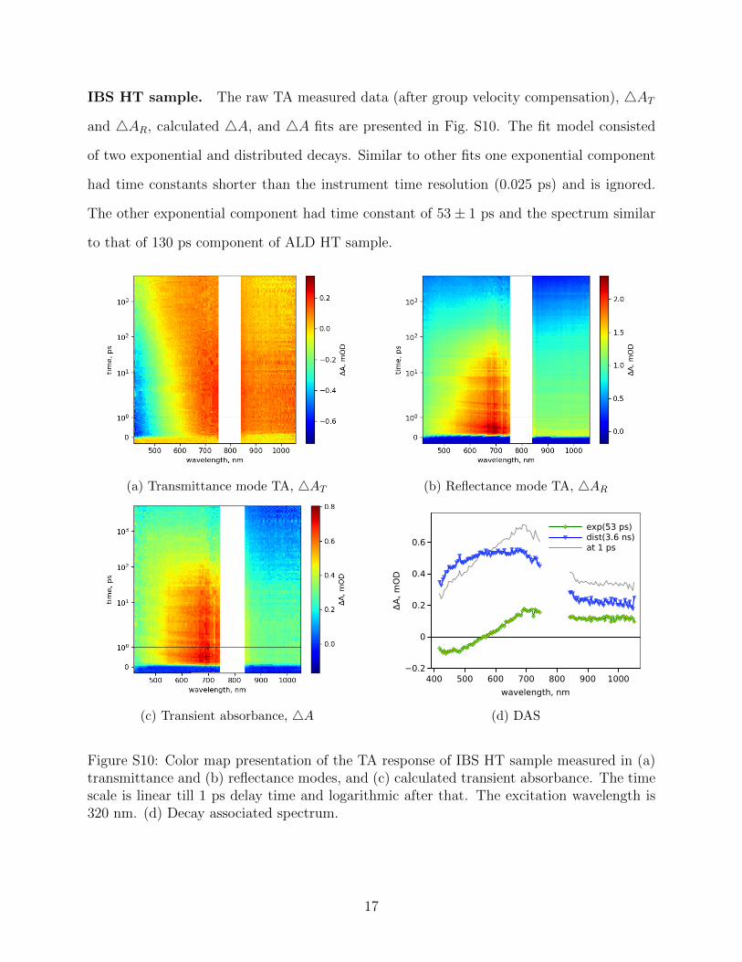
IBS HT sample. The raw TA measured data (after group velocity compensation), 4AT
and 4AR, calculated 4A, and 4A fits are presented in Fig. S10. The fit model consisted
of two exponential and distributed decays. Similar to other fits one exponential component
had time constants shorter than the instrument time resolution (0.025 ps) and is ignored.
The other exponential component had time constant of 53± 1 ps and the spectrum similar
to that of 130 ps component of ALD HT sample.
(a) Transmittance mode TA, 4AT (b) Reflectance mode TA, 4AR
(c) Transient absorbance, 4A
400 500 600 700 800 900 1000
wavelength, nm
−0.2
0
0.2
0.4
0.6
ΔA
, m
OD
exp(53 ps)dist(3.6 ns)at 1 ps
(d) DAS
Figure S10: Color map presentation of the TA response of IBS HT sample measured in (a)transmittance and (b) reflectance modes, and (c) calculated transient absorbance. The timescale is linear till 1 ps delay time and logarithmic after that. The excitation wavelength is320 nm. (d) Decay associated spectrum.
17

SPD as-deposited sample. The raw TA measured data (after group velocity compen-
sation), 4AT and 4AR, calculated 4A, and 4A fits are presented in Fig. S9. To obtain a
reasonably good fit a sum of exponential and distributed decays had to be used. The time
constant of exponential component is 1.6 ps which is much sorter than the central time con-
stant of the distributed decay, 50 ps, but the shapes of the components are only marginally
different.
(a) Transmittance mode TA, 4AT (b) Reflectance mode TA, 4AR
(c) Transient absorbance, 4A
400 500 600 700 800 900 1000
wavelength, nm
0
0.2
0.4
0.6
0.8
1
ΔA
, m
OD
exp(1.6 ps)dist(50 ps)at 0 ps
(d) DAS
Figure S11: Color map presentation of the TA response of SPD as-deposited sample measuredin (a) transmittance and (b) reflectance modes, and (c) calculated transient absorbance. Thetime scale is linear till 1 ps delay time and logarithmic after that. The excitation wavelengthis 320 nm. (d) Decay associated spectrum.
18

SPD HT sample. The raw TA measured data (after group velocity compensation), 4AT
and 4AR, calculated 4A, and 4A fits are presented in Fig. S12. The fit model consisted
of two exponential and distributed decays. Similar to other fits one exponential component
had time constants close to the instrument time resolution (0.13 ps) and is ignored. The
other exponential component had time constant of 98 ± 2 ps and spectrum similar to that
of 130 ps component of ALD HT sample.
(a) Transmittance mode TA, 4AT (b) Reflectance mode TA, 4AR
(c) Transient absorbance, 4A
400 500 600 700 800 900 1000
wavelength, nm
0
0.5
1
ΔA
, m
OD
at 1 psexp(98 ps)dist(1.4 ns)
(d) DAS
Figure S12: Color map presentation of the TA response of SPD HT sample measured in (a)transmittance and (b) reflectance modes, and (c) calculated transient absorbance. The timescale is linear till 1 ps delay time and logarithmic after that. The excitation wavelength is320 nm. (d) Decay associated spectrum.
19

5.2. Lifetime of thicker samples
Thicker films of 200 nm were prepared by ion beam sputtering to study the effect of TiO2
film thickness on the lifetime of different charge carrier components. The decay spectra of
these samples were also fitted by two exponential and one distributed decay component.
It was seen that increasing thickness of TiO2 layer does not play any significant role in
increasing the lifetime of photogenerated charge carriers and hence thicker films of TiO2 will
not provide any benefit to photocatalytic applications.
Table S3: Time constants for 200 nm as-dep. and HT IBS samples arising from global fitof the calculated 4A(λ, t) data, τ1 is exponential decay component, τd is distributed decaytime constant and δ is the relative distribution width.
Samples τ1, ps τd, ps (δ)IBS as-dep. 3 30 (100)IBS HT 56 1454 (69.1)
2 5 0 3 0 0 3 5 0 4 0 0 4 5 0 5 0 0 5 5 0 6 0 0 6 5 0 7 0 0 7 5 0 0 . 0 0 . 5 1 . 0 1 . 5 2 . 00 . 0
0 . 2
0 . 4
0 . 6
0 . 8
1 . 0
1 . 2
1 . 4a
Inten
sity (a
.u.)
W a v e l e n g h t ( n m )
E x c i t a t i o n s p e c t r u m i r r a d i a n c e M B a b s o r b a n c e 6 3 5 n m l a s e r
p r o b e
b
Abso
rbanc
e at 6
35 nm
M B c o n c e n t r a t i o n ( p p m )
M B i n 5 c m c u v e t t e L i n e a r f i t
� � � � � � � � � � � � � � � �
R 2 = 0 . 9 9 9
Figure S13: (a) Irradiance of the excitation light source, methylene blue (MB) absorbanceand the wavelength of probe laser (bandwidth < 1 nm). (b) MB calibration curve measuredin a cuvette with path length of 5 cm.
20

6. Methylene blue degradation
The excitation spectrum (300–400 nm) has only minor overlap with the methylene blue
absorption spectrum as shown in Figure S13, and therefore, the filter effect in the test was
small.
References
(1) Barybin, A.; Shapovalov, V. Substrate Effect on the Optical Reflectance and Transmit-
tance of Thin-Film Structures. Intern. J. Optics 2010, 137572.
(2) Shannon, R. D.; Shannon, R. C.; Medenbach, O.; Fischer, R. X. Refractive Index and
Dispersion of Fluorides and Oxides. J. Phys. Chem. Ref. Data 2002, 31, 931–970.
(3) Santos, H. A. Porous Silicon for Biomedical Applications ; 2014; pp 507–526.
(4) Berberan-Santos, M. N.; Borisov, E. N.; Valeur, B. Mathematical functions for the anal-
ysis of luminescence decays with underlying distributions 1. Kohlrausch decay function
(stretched exponential). Chem. Phys. 2005, 315, 171–182.
21