CHARACTERIZATION OF THIN FILMS, SURFACES AND DEVICES · Emitter layer of a polycrystalline silicon...
6
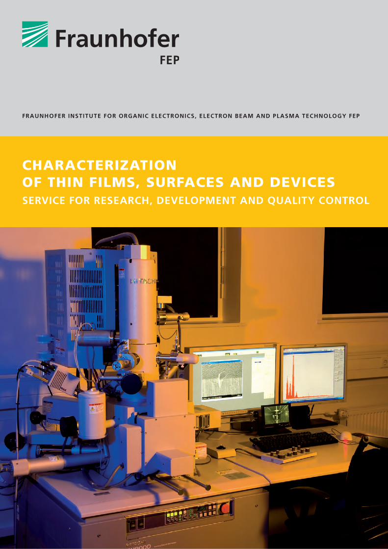
FRAUNHOFER INSTITUTE FOR ORGANIC ELECTRONICS, ELECTRON BEAM AND PLASMA TECHNOLOGY FEP CHARACTERIZATION OF THIN FILMS, SURFACES AND DEVICES SERVICE FOR RESEARCH, DEVELOPMENT AND QUALITY CONTROL
Transcript of CHARACTERIZATION OF THIN FILMS, SURFACES AND DEVICES · Emitter layer of a polycrystalline silicon...
FRAUNHOFER INSTITUTE FOR ORGANIC ELECTRONICS, ELECTRON BEAM AND PLASMA TECHNOLOGY FEP
CHARACTERIZATION OF THIN FILMS, SURFACES AND DEVICESSERVICE FOR RESEARCH, DEVELOPMENT AND QUALITY CONTROL

Structure and microstructure
The department materials analysis at
Fraunhofer FEP has versatile methods
for characterization of thin films and
surfaces. The equipment and the wide
Characterization of thin films and surfaces
analytical experience of our staff are
available for the product and technology
development of our institute and are
offered as a service to our customers.
Cross fracture and surface of a molybdenum layer (Topographic contrast)
Ion polished cross section of a permeation barrier layer system (Material contrast)
Emitter layer of a polycrystalline silicon solar cell (Voltage contrast)
Ion polished cross section of a CdTe solar cell (Crystal orientation contrast)
Ultra high resolution FE scanning
electron microscope, SU8000 (Hitachi)
Ion preparation technique for cross
sections, Cross Section Polisher,
SM-09010 (JEOL)
Metallographic preparation technique
and optical microscope Polyvar 2 Met
(Reichert)
Metallographic cross section of a copper layer
Metallographic cross section of a magnesium-zinc alloy layer
Typical applications areas are layers for
optics, sensor technology, displays,
photovoltaic, packaging, corrosion and
wear resistance.
21

Topography
Chemical composition
Surface of a FTO layer with typical crystallite morphology
Roughness scan of a steel sheet
Chemical depth profile of a CdTe thin film solar cell
Surface of a (Ti,Nb)OX layer with spherulitic crystallites
Stress determination of thin layers from curvature
Chemical depth profile of an optical rugate filter
Atomic force microscope (AFM) Explorer
(Topometrix)
Energy-dispersive X-ray spectroscopy (EDS)
SDD detector Apollo XV (EDAX)
Surface profiler P15-LS (TENCOR)
Glow discharge optical emission spectros-
copy (GD-OES)
GD-Profiler 2 (HORIBA Jobin Yvon)
750
500
250
0
-250
-500
-750
rou
gh
nes
s in
nm
scan length in µm0 250 500 750 1000
302520151050
-5-10
z in
µm
scan length in mm
difference
post-scan
pre-scan
0 10 20 30 40 50 60 70
3 4 5
EDS spectrum of a SiOXNY layer EDS spectrum of a (Zn, Sn)OX layer
6050403020100
2.0
1.5
1.0
0.5
0.0
con
cen
trat
ion
in a
t. %
inte
nsi
ty in
V
sputter depth in µm sputter time in sCd Te S Sn
Ta*5 Si*20 O*3 Ca NaO
Si Ca Na Ti
0 200 400 600 8000.0 0.5 1.0 1.5 2.0 2.5 3.0

Layer properties
T ITLE PHOTO
FE scanning electron microscope
SU8000 (Hitachi)
1 Metallographic preparation
technique (Struers)
2 Optical microscope
Polyvar 2 Met (Reichert)
3 Atomic force microscope
Explorer (Topometrix)
4 Surface profiler P15-LS (TENCOR)
5 Glow discharge optical emission
spectrometer GD-Profiler 2
(HORIBA Jobin Yvon)
6 Spectroscopic ellipsometer SE850
(Sentech)
7 Nano Indenter XP (MTS)
Optical Mechanical Electrical
▪ spectroscopic
ellipsometry
(SE850, Sentech)
▪ UV VIS spectroscopy
(Lambda 950,
Perkin Elmer)
▪ haze measurement
(Haze-guard plus,
BYK-Gardner)
▪ hardness and
indentation modulus
(Nano Indenter XP, MTS)
▪ abrasion resistance
(Taber Abraser)
▪ scratch adhesion test
(MST4, CSEM)
▪ layer thickness
(Calotest, CSEM)
▪ I-V curve of solar cells
(Sun 300, LOT)
▪ quantum efficiency
(Oriel IQE-200,
Newport)
▪ photo and dark
conductivity
(SUSS Prober und
Keithley)
▪ electrical four point
probe
(FPP 5000, Veeco)
Permeation barrier Corrosion Environmental
▪ water vapour
permeability
(WDDG, Brugger Fein-
mechanik; HiBarSens
2.0 HT, Sempa)
▪ electrical and optical
Calcium test
▪ oxygen permeability
(OX-TRAN 2/20,
Mocon)
▪ corrosion test system for
condensation water test
and salt spray test
(SKB 400 A-SC, Liebisch)
▪ environmental chamber
- 40 ... + 150°C;
adjustable humidity
(SH-241, ESPEC)
6 7
Fraunhofer Institute for
Organic Electronics, Electron Beam
and Plasma Technology FEP
Winterbergstr. 28
01277 Dresden, Germany
Contact persons
www.fep.fraunhofer.de
Dr. Olaf Zywitzki
Phone +49 351 2586-180
Dr. Thomas Modes
Phone +49 351 2586-183

▪ analytical services for analysis of the
effect of process parameters on
structure and microstructure, topo-
graphy, chemical composition and
properties of thin films
▪ support of our customers for quality
control and failure analysis
Our offer
Electro-optical device characterization
8 Water vapour permeability tester
(Brugger)
9 Calotest (CSEM)
10 Abrasion resistance (Taber Abraser)
11 Electrical conductivity
(SUSS Prober und Keithley)
▪ technical advice for selection and
combination of suitable analysis
methods
▪ development of analysis methods for
specific applications and measure-
ment tasks
8 9 10 11
▪ electro-optical characteristic within the visible range (380 to 800 nm) including
spectral and angular distribution
▪ luminance, quantum efficiency, luminous efficacy, color temperature,
and color point (e.g. following CIE1931)
▪ homogeneity of the luminance on large area
▪ direct measurement of the absolute luminous flux for panels up to about
1000 cm² active area
▪ high resolution IR images on large area
▪ transmission and reflection in the visible and near-infrared range
▪ emission and excitation spectra of organic materials within a spectral range of 200 to 850 nm
▪ determination of the luminance degradation, color shift as well as the drop-down rate of
OLED devices under long-term operation
▪ long-term measurements under standardized climatic conditions for the
determination of the shelf lifetime of OLED devices
▪ solar cell characterization (solar simulator, photocurrent-mapper MP15)
Luminance- / Current- voltage characteristic
OLED spectraDetermination of operational lifetime
102
101
100
10-1
10-2
10-3
10-4
10-5
10-6
Cu
rren
t D
ensi
ty [
mA
/cm
²]
Voltage [V]
2,6 V @100 cd/m²2,9 V @1000 cd/m²
105
104
103
102
101
-5 -4 -3 -2 -1 0 1 2 3 4 5
Lum
inan
ce [
cd/c
m²]
500 103 104 105
105
104
103
102
101
100
10-1
10-2
50%
Lif
etim
e [h
]
Start Luminance [cd/m²]
30 mA/cm² 60 mA/cm²
90 mA/cm²
120 mA/cm²
0,08
0,07
0,06
0,05
0,04
0,03
0,02
0,01
0,00
Spectrum @1700 cd/m²C.I.E. 0.36/0.34
Spec
t. R
adia
nce
[W
/(m
²·sr
·nm
)]
Wavelength [nm]300 400 500 600 700 800

© F R A U N H O F E R F E P – 2 . 3 – F 0 3
We focus on quality
and the ISO 9001.