BGS12AL7-4 DS Rev1.3
16
Chipsmall Limited consists of a professional team with an average of over 10 year of expertise in the distribution of electronic components. Based in Hongkong, we have already established firm and mutual-benefit business relationships with customers from,Europe,America and south Asia,supplying obsolete and hard-to-find components to meet their specific needs. With the principle of “Quality Parts,Customers Priority,Honest Operation,and Considerate Service”,our business mainly focus on the distribution of electronic components. Line cards we deal with include Microchip,ALPS,ROHM,Xilinx,Pulse,ON,Everlight and Freescale. Main products comprise IC,Modules,Potentiometer,IC Socket,Relay,Connector.Our parts cover such applications as commercial,industrial, and automotives areas. We are looking forward to setting up business relationship with you and hope to provide you with the best service and solution. Let us make a better world for our industry! Contact us Tel: +86-755-8981 8866 Fax: +86-755-8427 6832 Email & Skype: [email protected] Web: www.chipsmall.com Address: A1208, Overseas Decoration Building, #122 Zhenhua RD., Futian, Shenzhen, China
Transcript of BGS12AL7-4 DS Rev1.3

Chipsmall Limited consists of a professional team with an average of over 10 year of expertise in the distribution
of electronic components. Based in Hongkong, we have already established firm and mutual-benefit business
relationships with customers from,Europe,America and south Asia,supplying obsolete and hard-to-find components
to meet their specific needs.
With the principle of “Quality Parts,Customers Priority,Honest Operation,and Considerate Service”,our business
mainly focus on the distribution of electronic components. Line cards we deal with include
Microchip,ALPS,ROHM,Xilinx,Pulse,ON,Everlight and Freescale. Main products comprise
IC,Modules,Potentiometer,IC Socket,Relay,Connector.Our parts cover such applications as commercial,industrial,
and automotives areas.
We are looking forward to setting up business relationship with you and hope to provide you with the best service
and solution. Let us make a better world for our industry!
Contact usTel: +86-755-8981 8866 Fax: +86-755-8427 6832
Email & Skype: [email protected] Web: www.chipsmall.com
Address: A1208, Overseas Decoration Building, #122 Zhenhua RD., Futian, Shenzhen, China

Industr ia l & Mult imarket
Data Sheet
Revision 1.3, 2009-06-24
Preliminary
BGS12AL7-4SPDT RF Switch

Edition 2009-06-24
Published byInfineon Technologies AG81726 Munich, Germany
© 2009 Infineon Technologies AGAll Rights Reserved.
Legal Disclaimer
The information given in this document shall in no event be regarded as a guarantee of conditions or characteristics. With respect to any examples or hints given herein, any typical values stated herein and/or any information regarding the application of the device, Infineon Technologies hereby disclaims any and all warranties and liabilities of any kind, including without limitation, warranties of non-infringement of intellectual property rights of any third party.
Information
For further information on technology, delivery terms and conditions and prices, please contact the nearest Infineon Technologies Office (www.infineon.com).
Warnings
Due to technical requirements, components may contain dangerous substances. For information on the types in question, please contact the nearest Infineon Technologies Office.
Infineon Technologies components may be used in life-support devices or systems only with the express written approval of Infineon Technologies, if a failure of such components can reasonably be expected to cause the failure of that life-support device or system or to affect the safety or effectiveness of that device or system. Life support devices or systems are intended to be implanted in the human body or to support and/or maintain and sustain and/or protect human life. If they fail, it is reasonable to assume that the health of the user or other persons may be endangered.

BGS12AL7-4SPDT RF Switch
Preliminary Data Sheet 3 Revision 1.3, 2009-06-24
Trademarks of Infineon Technologies AG
APOXI™, BlueMoon™, COMNEON™, CONVERGATE™, COSIC™, C166™, CROSSAVE™, CanPAK™,
CIPOS™, CoolMOS™, CoolSET™, CORECONTROL™, DAVE™, EasyPIM™, EconoBRIDGE™,
EconoDUAL™, EconoPACK™, EconoPIM™, EiceDRIVER™, EUPEC™, FCOS™, FALC™, GEMINAX™,
GOLDMOS™, HITFET™, HybridPACK™, ISAC™, ISOFACE™, IsoPACK™, my-d™, MIPAQ™, ModSTACK™,
NovalithIC™, OmniTune™, OmniVia™, OPTIVERSE™, OptiMOS™, ORIGA™, PROFET™, PRO-SIL™,
PrimePACK™, RASIC™, ReverSave™, SCEPTRE™, SEROCCO™, SICOFI™, SMARTi™, SMINT™,
SOCRATES™, SatRIC™, SensoNor™, SINDRION™, SmartLEWIS™, SIEGET™, TrueNTRY™, TEMPFET™,
TriCore™, thinQ!™, TRENCHSTOP™, VINAX™, VINETIC™, X-GOLD™, XMM™, X-PMU™, XPOSYS™,
XWAY™.
Other Trademarks
AMBA™, ARM™, MULTI-ICE™, PRIMECELL™, REALVIEW™, THUMB™ of ARM Limited, UK. AUTOSAR™ is
licensed by AUTOSAR development partnership. Bluetooth™ of Bluetooth SIG Inc. CAT-iq™ of DECT Forum.
COLOSSUS™, FirstGPS™ of Trimble Navigation Ltd. EMV™ of EMVCo, LLC (Visa Holdings Inc.). EPCOS™ of
Epcos AG. FLEXGO™ of Microsoft Corporation. FlexRay™ is licensed by FlexRay Consortium.
HYPERTERMINAL™ of Hilgraeve Incorporated. IEC™ of Commission Electrotechnique Internationale. IrDA™ of
Infrared Data Association Corporation. ISO™ of INTERNATIONAL ORGANIZATION FOR STANDARDIZATION.
MATLAB™ of MathWorks, Inc. MAXIM™ of Maxim Integrated Products, Inc. MICROTEC™, NUCLEUS™ of
Mentor Graphics Corporation. Mifare™ of NXP. MIPI™ of MIPI Alliance, Inc. MIPS™ of MIPS Technologies, Inc.,
USA. muRata™ of MURATA MANUFACTURING CO. OmniVision™ of OmniVision Technologies, Inc.
Openwave™ Openwave Systems Inc. RED HAT™ Red Hat, Inc. RFMD™ RF Micro Devices, Inc. SIRIUS™ of
Sirius Sattelite Radio Inc. SOLARIS™ of Sun Microsystems, Inc. SPANSION™ of Spansion LLC Ltd. Symbian™
of Symbian Software Limited. TAIYO YUDEN™ of Taiyo Yuden Co. TEAKLITE™ of CEVA, Inc. TEKTRONIX™
of Tektronix Inc. TOKO™ of TOKO KABUSHIKI KAISHA TA. UNIX™ of X/Open Company Limited. VERILOG™,
PALLADIUM™ of Cadence Design Systems, Inc. VLYNQ™ of Texas Instruments Incorporated. VXWORKS™,
WIND RIVER™ of WIND RIVER SYSTEMS, INC. ZETEX™ of Diodes Zetex Limited.
Last Trademarks Update 2009-05-27
BGS12AL7-4 SPDT RF Switch
Revision History: 2009-06-24, Revision 1.3
Previous Revision: 2008-10-08, V1.2
Page Subjects (major changes since last revision)
Converted to the new IFX Template.
9 Extended Supply Voltage Range
10 Pin Description Pin 7
11 Electrical Specifications @ 100 MHz
12 Correct Return Loss and Isolation axis label
14 Update Board Pad (SMD) & Apertures, Tape and Reel Info

BGS12AL7-4SPDT RF Switch
Table of Contents
Preliminary Data Sheet 4 Revision 1.3, 2009-06-24
Table of Contents . . . . . . . . . . . . . . . . . . . . . . . . . . . . . . . . . . . . . . . . . . . . . . . . . . . . . . . . . . . . . . . . 4
List of Figures . . . . . . . . . . . . . . . . . . . . . . . . . . . . . . . . . . . . . . . . . . . . . . . . . . . . . . . . . . . . . . . . . . . 5
List of Tables . . . . . . . . . . . . . . . . . . . . . . . . . . . . . . . . . . . . . . . . . . . . . . . . . . . . . . . . . . . . . . . . . . . . 6
1 Features . . . . . . . . . . . . . . . . . . . . . . . . . . . . . . . . . . . . . . . . . . . . . . . . . . . . . . . . . . . . . . . . . . . . . . . . 7
2 Maximum Ratings . . . . . . . . . . . . . . . . . . . . . . . . . . . . . . . . . . . . . . . . . . . . . . . . . . . . . . . . . . . . . . . . 9
3 Pin Description . . . . . . . . . . . . . . . . . . . . . . . . . . . . . . . . . . . . . . . . . . . . . . . . . . . . . . . . . . . . . . . . . 10
4 Electrical Specifications . . . . . . . . . . . . . . . . . . . . . . . . . . . . . . . . . . . . . . . . . . . . . . . . . . . . . . . . . 11
5 Measurement Results . . . . . . . . . . . . . . . . . . . . . . . . . . . . . . . . . . . . . . . . . . . . . . . . . . . . . . . . . . . . 12
6 Package Outlines . . . . . . . . . . . . . . . . . . . . . . . . . . . . . . . . . . . . . . . . . . . . . . . . . . . . . . . . . . . . . . . 14
Table of Contents

BGS12AL7-4SPDT RF Switch
List of Figures
Preliminary Data Sheet 5 Revision 1.3, 2009-06-24
Figure 1 Functional Diagram. . . . . . . . . . . . . . . . . . . . . . . . . . . . . . . . . . . . . . . . . . . . . . . . . . . . . . . . . . . . . . 8
Figure 2 Pin Configuration (top view) . . . . . . . . . . . . . . . . . . . . . . . . . . . . . . . . . . . . . . . . . . . . . . . . . . . . . . 10
Figure 3 Measurement Results (@ T = 25°C) . . . . . . . . . . . . . . . . . . . . . . . . . . . . . . . . . . . . . . . . . . . . . . . 12
Figure 4 Application Board: No External Components Necessary . . . . . . . . . . . . . . . . . . . . . . . . . . . . . . . . 13
Figure 5 Deembedding Board . . . . . . . . . . . . . . . . . . . . . . . . . . . . . . . . . . . . . . . . . . . . . . . . . . . . . . . . . . . 13
Figure 6 Package TSLP7-4. . . . . . . . . . . . . . . . . . . . . . . . . . . . . . . . . . . . . . . . . . . . . . . . . . . . . . . . . . . . . . 14
Figure 7 Board Pad (SMD) & Apertures . . . . . . . . . . . . . . . . . . . . . . . . . . . . . . . . . . . . . . . . . . . . . . . . . . . . 14
Figure 8 Tape and Reel . . . . . . . . . . . . . . . . . . . . . . . . . . . . . . . . . . . . . . . . . . . . . . . . . . . . . . . . . . . . . . . . 14
List of Figures

BGS12AL7-4SPDT RF Switch
List of Tables
Preliminary Data Sheet 6 Revision 1.3, 2009-06-24
Table 1 Maximum Ratings . . . . . . . . . . . . . . . . . . . . . . . . . . . . . . . . . . . . . . . . . . . . . . . . . . . . . . . . . . . . . . 9
Table 2 Operation Ranges . . . . . . . . . . . . . . . . . . . . . . . . . . . . . . . . . . . . . . . . . . . . . . . . . . . . . . . . . . . . . . 9
Table 3 Pin Description . . . . . . . . . . . . . . . . . . . . . . . . . . . . . . . . . . . . . . . . . . . . . . . . . . . . . . . . . . . . . . . . 10
Table 4 Truth Table . . . . . . . . . . . . . . . . . . . . . . . . . . . . . . . . . . . . . . . . . . . . . . . . . . . . . . . . . . . . . . . . . . 10
Table 5 Electrical Characteristics . . . . . . . . . . . . . . . . . . . . . . . . . . . . . . . . . . . . . . . . . . . . . . . . . . . . . . . . 11
List of Tables

12
3
65
4
7
Product Name Package Chip Marking
BGS12AL7-4 TSLP7-4 M4781 12
SPDT RF Switch
BGS12AL7-4
Preliminary Data Sheet 7 Revision 1.3, 2009-06-24
1 Features
Main features:
� Low insertion loss
� High port-to-port-isolation
� Low harmonic generation
� On-chip control logic
� High ESD robustness
� No external components required
� General purpose switch for applications up to 3 GHz
� Small leadless package TSLP-7-6
� Lead and halogen free package (RoHS and WEEE compliant)
Description
The BGS12AL7-4 General Purpose RF MOS switch is designed to cover a broad range of applications from
30 MHz to 3 GHz. The symmetric design of its single pole double throw configuration, as shown in Figure 1 offers
high design flexibility. This single supply chip integrates on-chip CMOS logic driven by a simple, single-pin CMOS
or TTL compatible control input signal. The 0.1 dB compression point exceeds the switch’s maximum input power
level of 21 dBm, resulting in linear performance at all signal levels. The RF switch has a very low insertion loss of
0.4 dB in the 1 GHz and 0.5 dB in the 2 GHz range.
Unlike GaAs technology, external DC blocking capacitors at the RF ports are only required if DC voltage is applied
externally.

BGS12AL7-4SPDT RF Switch
Features
Preliminary Data Sheet 8 Revision 1.3, 2009-06-24
The BGS12AL7-4 RF switch is manufactured in Infineon’s patented MOS technology, offering the performance of
GaAs with the economy and integration of conventional CMOS including the inherent higher ESD robustness.
Figure 1 Functional Diagram

BGS12AL7-4SPDT RF Switch
Maximum Ratings
Preliminary Data Sheet 9 Revision 1.3, 2009-06-24
2 Maximum Ratings
Attention: Stresses above the max. values listed here may cause permanent damage to the device.
Exposure to absolute maximum rating conditions for extended periods may affect device
reliability. Maximum ratings are absolute ratings; exceeding only one of these values may
cause irreversible damage to the integrated circuit.
Table 1 Maximum Ratings
Parameter Symbol Values Unit Note /
Test ConditionMin. Typ. Max.
Storage temperature range Tstg -65 – 150 °C –
DC Voltage at all pins to GND VDC – – 5 V –
RF power max. at all RF ports PIN – – 24 dBm –
ESD Capability
Human Body Model IEC61340-3-1 VESD – – 1000 V –
Machine Model IEC61340-3-2 – – 100 V –
Table 2 Operation Ranges
Parameter Symbol Values Unit Note /
Test ConditionMin. Typ. Max.
Ambient temperature TA -30 – 85 °C –
RF Frequency f 0.03 – 3 GHz –
Control voltage low VCtrL -0.3 – 0.3 V –
Control voltage high VCtrlH 1.4 – Vdd V –
Supply voltage1)
1) Supply voltage must be connected before Control Voltage
Vdd 2.4 – 3.6 V –
Current consumption Vdd Pin (over
temperature)
IVdd 80 – 350 μA –
Current Consumption Vctrl Pin ICtrl – – 30 μA –
Power Range Pin – – – dBm –
(VSWR ∞: 1) – – 15 –
(VSWR 3: 1) – – 18 –
(VSWR 1: 1) – – 21 –

BGS12AL7-4SPDT RF Switch
Pin Description
Preliminary Data Sheet 10 Revision 1.3, 2009-06-24
3 Pin Description
Figure 2 Pin Configuration (top view)
Table 3 Pin Description
Pin No. Name Pin
Type
Buffer
Type
Function
1 RF2 I/O RF Port 2 Out
2 GND GND Ground
3 RF1 I/O RF Port 1 Out
4 Vdd PWR Supply Voltage
5 RFIN I/O RF Port In
6 CTRL I Control Pin
7 NC NC It is recommended to connect Pin 7 to Ground
Table 4 Truth Table
Ctrl 1 RF 1 RF 2
0 1 0
1 0 1
TSLP7-4.vsd
Ctrl
RF2
Vdd
RF1
RFin
GND
2 3
456
7
Gnd
1

BGS12AL7-4SPDT RF Switch
Electrical Specifications
Preliminary Data Sheet 11 Revision 1.3, 2009-06-24
4 Electrical Specifications
Test Conditions:
� Termination port impedance: Z0 = 50 Ω� Temperature range: TA = -30 °C...+85 °C
� Supply Voltage: Vdd = 2.8 V
� Pin = 15 dBm
� Across operating range of control voltages: VCtrH = 1.4...2.8 V
Table 5 Electrical Characteristics
Parameter Symbol Values Unit Note / Test Condition
Min. Typ. Max.
Insertion Loss IL – 0.31)2)
1) @TA= 25 °C
2) Not measured in production, verified by design
– dB f = 0.1 GHz TX,
– 0.41) – dB f = 1 GHz TX,
– 0.51) – dB f = 2 GHz TX,
Return Loss RL – 302) – dB f = 0.1 GHz
15 22 – dB f = 1 GHz
13 22 – dB f = 2 GHz
Isolation RFin - RF1 ISORFin-RF1 – 502) – dB f = 0.1 GHz
22 32 – dB f = 1 GHz
18 25 – dB f = 2 GHz
Isolation RFin - RF2 ISORFin-RF2 – 502) – dB f = 0.1 GHz
22 32 – dB f = 1 GHz
18 25 – dB f = 2 GHz
Isolation RF1 - RF2 ISORF1-RF2 – 502) – dB f = 0.1 GHz
24 32 – dB f = 1 GHz
18 25 – dB f = 2 GHz
Isolation RF ports - Vdd, Vctrl ISORF-DC 25 302) – dB f = 1 GHz
15 202) – dB f = 2 GHz
Harmonic Generation up to 12.75 GHz PHarm – -752) -50 dBm f = 1 GHz
– -802) -50 dBm f = 2 GHz
On Switching Time (10-90%) RF ton – 32) 5 μs f = 1 GHz
Off Switching Time (10-90%) RF toff – 0.52) 5 μs f = 1 GHz
Current Consumption at Vdd Pin Idd – 120 – μA –
Input 0.1 dB compression P0.1dB 212) – – dBm f = 1 GHz
BGS12AL7-4SPDT RF Switch
Measurement Results
Preliminary Data Sheet 12 Revision 1.3, 2009-06-24
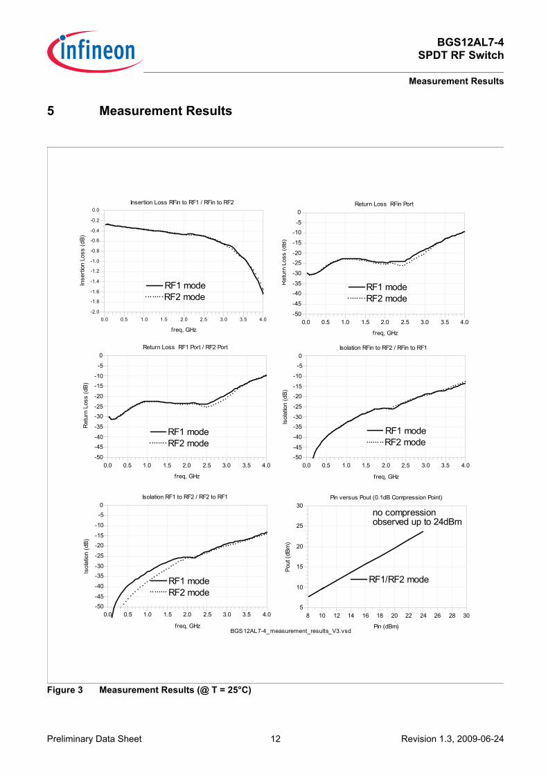
5 Measurement Results
Figure 3 Measurement Results (@ T = 25°C)
BGS12AL7-4_measurement_results_V3.vsd
0.5 1.0 1.5 2.0 2.5 3.0 3.50.0 4.0
-1.8
-1.6
-1.4
-1.2
-1.0
-0.8
-0.6
-0.4
-0.2
-2.0
0.0
freq, GHz
Insert
ion L
oss (
dB
)
Insertion Loss RFin to RF1 / RFin to RF2
0.5 1.0 1.5 2.0 2.5 3.0 3.50.0 4.0
-45
-40
-35
-30
-25
-20
-15
-10
-5
-50
0
freq, GHz
Retu
rn L
oss (
dB
)
Return Loss RFin Port
0.5 1.0 1.5 2.0 2.5 3.0 3.50.0 4.0
-45
-40
-35
-30
-25
-20
-15
-10
-5
-50
0
freq, GHz
Retu
rn L
oss (
dB
)
Return Loss RF1 Port / RF2 Port
0.5 1.0 1.5 2.0 2.5 3.0 3.50.0 4.0
-45
-40
-35
-30
-25
-20
-15
-10
-5
-50
0
freq, GHz
Isola
tion (
dB
)
Isolation RFin to RF2 / RFin to RF1
0.5 1.0 1.5 2.0 2.5 3.0 3.50.0 4.0
-45
-40
-35
-30
-25
-20
-15
-10
-5
-50
0
freq, GHz
Isola
tion (
dB
)
Isolation RF1 to RF2 / RF2 to RF1
RF1 mode
RF2 modeRF1 mode
RF2 mode
RF1 mode
RF2 mode
RF1 mode
RF2 mode
RF1 mode
RF2 mode
10 12 14 16 18 20 22 24 26 288 30
10
15
20
25
5
30
Pin (dBm)
Pout (d
Bm
)
Pin versus Pout (0.1dB Compression Point)
RF1/RF2 mode
no compressionobserved up to 24dBm

BGS12AL7-4SPDT RF Switch
Measurement Results
Preliminary Data Sheet 13 Revision 1.3, 2009-06-24
Application Board
Figure 4 Application Board: No External Components Necessary
Figure 5 Deembedding Board
BGS12 AL7-4 _application_ board .vsd
BGS 12AL 7-4_application _deembedding _board .vsd
BGS12AL7-4SPDT RF Switch
Package Outlines
Preliminary Data Sheet 14 Revision 1.3, 2009-06-24
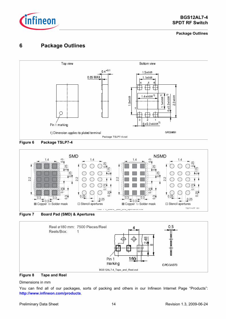
6 Package Outlines
Figure 6 Package TSLP7-4
Figure 7 Board Pad (SMD) & Apertures
Figure 8 Tape and Reel
Dimensions in mm
You can find all of our packages, sorts of packing and others in our Infineon Internet Page “Products”:
http://www.infineon.com/products.
Package TSLP7-4.vsd
TSLP7-4_board_ pad_and_apertures.vsd
SMD NSMD
BGS12AL7-4_Tape_and_Reel.vsd
0.5

Published by Infineon Technologies AG
w w w . i n f i n e o n . c o m