Auger Electron Spectroscopy and Its Application to ......Applications Since the introduction of...
4
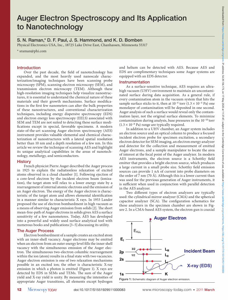
doi:10.1017/S1551929511000083 12 www.microscopy-today.com • 2011 March Auger Electron Spectroscopy and Its Application to Nanotechnology S. N. Raman,* D. F. Paul, J. S. Hammond, and K. D. Bomben Physical Electronics USA, Inc., 18725 Lake Drive East, Chanhassen, Minnesota 55317 * [email protected] Introduction Over the past decade, the field of nanotechnology has expanded, and the most heavily used nanoscale charac- terization/imaging techniques have been scanning probe microscopy (SPM), scanning electron microscopy (SEM), and transmission electron microscopy (TEM). Although these high-resolution imaging techniques help visualize nanostruc- tures, it is essential to understand the chemical nature of these materials and their growth mechanisms. Surface modifica- tions in the first few nanometers can alter the bulk properties of these nanostructures, and conventional characterization techniques, including energy dispersive spectroscopy (EDS) and electron energy loss spectroscopy (EELS) associated with SEM and TEM are not suited to detecting these surface modi- fications except in special, favorable specimens. A modern state-of-the-art scanning Auger electron spectroscopy (AES) instrument provides valuable elemental and chemical charac- terization of nanostructures with a lateral spatial resolution better than 10 nm and a depth resolution of a few nm. In this article we review the technique of scanning AES and highlight its unique analytical capabilities in the areas of nanotech- nology, metallurgy, and semiconductors. History French physicist Pierre Auger described the Auger process in 1925 to explain the radiationless relaxation of excited atoms observed in a cloud chamber [1]. Following ejection of a core-level electron by the incident electron beam (ioniza- tion), the target atom will relax to a lower energy state by a rearrangement of internal atomic electrons and the emission of an Auger electron. e energy of the Auger electron is charac- teristic of the target atom and allows elemental identification in a manner similar to characteristic X rays. In 1953 Lander proposed the use of electron bombardment in high vacuum as a means of observing Auger emission from solids [2]. e short mean-free-path of Auger electrons in solids gives AES a surface sensitivity of a few nanometeres. Today, AES has developed into a powerful and widely used surface analytical tool with numerous books and publications [3–5] discussing its utility. The Auger Process Electron bombardment of a sample creates an excited atom with an inner-shell vacancy. Auger electrons may be emitted when an electron from an outer energy level fills the inner shell vacancy with the simultaneous emission of the Auger elec- tron. e simultaneous two-electron columbic rearrangement within the ion (atom) results in a final state with two vacancies. Auger electron emission is one of two relaxation mechanisms possible in an excited ion; the other is characteristic X-ray emission in which a photon is emitted (Figure 1). X rays are detected by EDS in SEMs and TEMs. e sum of the Auger yield and X-ray yield is unity. By measuring the intensities of appropriate Auger transitions, all elements except hydrogen and helium can be detected with AES. Because AES and EDS are complimentary techniques some Auger systems are equipped with an EDS detector. Instrumentation As a surface-sensitive technique, AES requires an ultra- high vacuum (UHV) environment to maintain an uncontami- nated surface during data acquisition. As a general rule, if every contamination atom in the vacuum system that hits the sample surface sticks to it, then at 10 –6 torr (1.3 × 10 –4 Pa) one monolayer of contamination will be deposited in one second. Auger analysis of such a surface would reveal only the contam- ination layer, not the original surface elements. To minimize contamination during analysis, base pressures in the 10 –10 torr (1.3 × 10 –8 Pa) range are typically required. In addition to a UHV chamber, an Auger system includes an electron source and an optical column to produce a focused incident electron probe for specimen excitation, a secondary electron detector for SEM imaging, an electron energy analyzer and detector for the collection and measurement of emitted Auger electrons, and a sample manipulator to locate the area of interest at the focal point of the Auger analyzer. In modern AES instruments, the electron source is a Schottky field emitter that provides a bright electron source, which produces a large current in a small probe size. Schottky field emission sources can provide 1 nA of current into probe diameters on the order of 7 nm (70 Å). Although this is a lower current than was used for the previous generation of Auger instruments, it is sufficient when used in conjunction with parallel detection in the AES analyzer. Two different types of electron analyzers are typically used: the cylindrical mirror analyzer (CMA) and the spherical capacitor analyzer (SCA). e configuration schematics for these analyzers in the specimen chamber are shown in Fig- ure 2. In a CMA-based AES system, the electron gun is coaxial Figure 1: Schematic diagram of Auger electron emission. Downloaded from https://www.cambridge.org/core. IP address: 54.39.106.173, on 17 May 2020 at 11:37:47, subject to the Cambridge Core terms of use, available at https://www.cambridge.org/core/terms. https://doi.org/10.1017/S1551929511000083
Transcript of Auger Electron Spectroscopy and Its Application to ......Applications Since the introduction of...
doi:10.1017/S155192951100008312 www.microscopy-today.com • 2011 March
Auger Electron Spectroscopy and Its Application to Nanotechnology
S. N. Raman,* D. F. Paul, J. S. Hammond, and K. D. BombenPhysical Electronics USA, Inc., 18725 Lake Drive East, Chanhassen, Minnesota 55317* [email protected]
IntroductionOver the past decade, the field of nanotechnology has
expanded, and the most heavily used nanoscale charac-terization/imaging techniques have been scanning probe microscopy (SPM), scanning electron microscopy (SEM), and transmission electron microscopy (TEM). Although these high-resolution imaging techniques help visualize nanostruc-tures, it is essential to understand the chemical nature of these materials and their growth mechanisms. Surface modifica-tions in the first few nanometers can alter the bulk properties of these nanostructures, and conventional characterization techniques, including energy dispersive spectroscopy (EDS) and electron energy loss spectroscopy (EELS) associated with SEM and TEM are not suited to detecting these surface modi- fications except in special, favorable specimens. A modern state-of-the-art scanning Auger electron spectroscopy (AES) instrument provides valuable elemental and chemical charac-terization of nanostructures with a lateral spatial resolution better than 10 nm and a depth resolution of a few nm. In this article we review the technique of scanning AES and highlight its unique analytical capabilities in the areas of nanotech-nology, metallurgy, and semiconductors.History
French physicist Pierre Auger described the Auger process in 1925 to explain the radiationless relaxation of excited atoms observed in a cloud chamber [1]. Following ejection of a core-level electron by the incident electron beam (ioniza- tion), the target atom will relax to a lower energy state by a rearrangement of internal atomic electrons and the emission of an Auger electron. The energy of the Auger electron is charac-teristic of the target atom and allows elemental identification in a manner similar to characteristic X rays. In 1953 Lander proposed the use of electron bombardment in high vacuum as a means of observing Auger emission from solids [2]. The short mean-free-path of Auger electrons in solids gives AES a surface sensitivity of a few nanometeres. Today, AES has developed into a powerful and widely used surface analytical tool with numerous books and publications [3–5] discussing its utility.The Auger Process
Electron bombardment of a sample creates an excited atom with an inner-shell vacancy. Auger electrons may be emitted when an electron from an outer energy level fills the inner shell vacancy with the simultaneous emission of the Auger elec- tron. The simultaneous two-electron columbic rearrangement within the ion (atom) results in a final state with two vacancies. Auger electron emission is one of two relaxation mechanisms possible in an excited ion; the other is characteristic X-ray emission in which a photon is emitted (Figure 1). X rays are detected by EDS in SEMs and TEMs. The sum of the Auger yield and X-ray yield is unity. By measuring the intensities of appropriate Auger transitions, all elements except hydrogen
and helium can be detected with AES. Because AES and EDS are complimentary techniques some Auger systems are equipped with an EDS detector. Instrumentation
As a surface-sensitive technique, AES requires an ultra- high vacuum (UHV) environment to maintain an uncontami-nated surface during data acquisition. As a general rule, if every contamination atom in the vacuum system that hits the sample surface sticks to it, then at 10–6 torr (1.3 × 10⁻⁴ Pa) one monolayer of contamination will be deposited in one second. Auger analysis of such a surface would reveal only the contam-ination layer, not the original surface elements. To minimize contamination during analysis, base pressures in the 10–10 torr (1.3 × 10⁻⁸ Pa) range are typically required.
In addition to a UHV chamber, an Auger system includes an electron source and an optical column to produce a focused incident electron probe for specimen excitation, a secondary electron detector for SEM imaging, an electron energy analyzer and detector for the collection and measurement of emitted Auger electrons, and a sample manipulator to locate the area of interest at the focal point of the Auger analyzer. In modern AES instruments, the electron source is a Schottky field emitter that provides a bright electron source, which produces a large current in a small probe size. Schottky field emission sources can provide 1 nA of current into probe diameters on the order of 7 nm (70 Å). Although this is a lower current than was used for the previous generation of Auger instruments, it is sufficient when used in conjunction with parallel detection in the AES analyzer.
Two different types of electron analyzers are typically used: the cylindrical mirror analyzer (CMA) and the spherical capacitor analyzer (SCA). The configuration schematics for these analyzers in the specimen chamber are shown in Fig- ure 2. In a CMA-based AES system, the electron gun is coaxial
Figure 1: Schematic diagram of Auger electron emission.
Dow
nloaded from https://w
ww
.cambridge.org/core . IP address: 54.39.106.173 , on 17 M
ay 2020 at 11:37:47 , subject to the Cambridge Core term
s of use, available at https://ww
w.cam
bridge.org/core/terms . https://doi.org/10.1017/S1551929511000083

132011 March • www.microscopy-today.com
backscatter factors, chemical effects on peak shapes and intensities, and surface roughness. Although this approach is useful in measuring the relative number of atoms of an element, one must be aware that the microscopic character of complex chemical systems has a strong effect on the accuracy of the results.
AES spectroscopy at high spatial resolution requires high stability in the electron beam over the long acquisition times required in some cases to obtain high elemental sensitivity. This is illustrated in the Auger maps from an AlGaAs/GaAs super-lattice sample (Figure 3). The Al map was acquired over 24 hours to illustrate the high-sensitivity
analytical capability of an Auger system. This analysis clearly reveals the 4-nm Al layer in the structure.
Because AES is a surface-sensitive technique, most AES instruments employ an in-situ Ar ion sputter gun to remove material from the surface of the specimen and characterize the composition as a function of sputter depth. State-of-the-art sputter ion guns with neutral atom rejection and low ion-beam voltage have the ability to remove less than 0.5 nm (5 Å) and characterize the exposed specimen surface. Sputter etching is frequently used to remove surface contaminants prior to analysis. Applications
Since the introduction of commercial AES instruments 40 years ago, applications areas have expanded greatly, particularly
Auger Electron Spectroscopy
with the analyzer and provides both the sensitivity and unobstructed view needed to fully characterize microstruc- tures and nanostructures with significant sample topography. Figure 2 shows the secondary electron images and Auger intensity maps for powder metallurgy samples obtained with the two different analyzer geometries. The CMA system geometry allows the secondary electron image and corresponding Auger image to have high and uniform sensitivities from all sides of the imaged structures; whereas, shadowing is observed in AES images collected using the SCA geometry. SCA-based AES instruments have good energy resolution for chemical state analysis, but recent advances in CMA technology now provide similar energy resolution without sacrificing the Auger imaging advantages of the CMA coaxial geometry.
It is possible to quantify the Auger signals so as to determine the relative concen- trations of the elements pre- sent by measuring the signal intensity of each element [6]. For a given type of analyzer, correction factors (determined using elemental standards at a specific primary excitation energy) will account for differ-ences in the electron impact ionization cross sections. Thus, a simple calculation will create a table of relative surface com- positions. In this manner, all observed elements may be measured with detection limits down to 0.1 atomic percent. It is to be noted that the errors inherent in this approach include matrix effects related to electron escape depth and
Figure 2: SEM images and Ni Auger maps from a coaxial CMA analyzer (left) and a non-coaxial SCA analyzer (right).
Figure 3: High spatial resolution Auger mapping for Ga (left) and Al (right) on an AlGaAs/GaAs (structure provided by BAM, Germany).
Dow
nloaded from https://w
ww
.cambridge.org/core . IP address: 54.39.106.173 , on 17 M
ay 2020 at 11:37:47 , subject to the Cambridge Core term
s of use, available at https://ww
w.cam
bridge.org/core/terms . https://doi.org/10.1017/S1551929511000083

14 www.microscopy-today.com • 2011 March
Auger Electron Spectroscopy
STEM/EELS analyses of these nanocones are only able to identify the bulk elemental composition of the structures. High-resolution AES helps to reveal a non-uniform surface chemical composition among several different nanocones. The SEM image (Figure 4a), the nitrogen image (Figure 4b), the iron image (Figure 4c), and the Fe and N overlay image (Fig- ure 4d) help to highlight the elemental information available, without imaging artifacts introduced by the nanocone shape. This information is crucial in understanding the growth mechanisms of these nanostructures.
Surface and grain boundary segregation is of signif-icant importance in the metallurgical industry. Segregated nanolayers with low concentrations of elements such as B or P are not easy to detect in X-ray spectrometry by EDS. A steel sample containing 1.02 at. % Mn and 0.05 at. % B was annealed in a 5% H2/N2 environment at 800°C. The resulting segregation on the surface was studied with AES. High spatial resolution Auger maps (Figure 5) reveal preferential segregation of Mn and B to regions with enhanced oxidation. An Auger spectrum from the region of enhanced Mn and B (Figure 6) confirms the segregation showing 10.7 atomic % Mn and 7.9 atomic % B present on the sample surface; these numbers are much higher than the amounts added into the alloy.
Doped silicon nanowire (SiNW) based FET devices are being evaluated as promising candidates for replacing tradi- tional MOSFETs, prompting a requirement to understand their unique electronic properties [6]. The SiNWs produced for this study were grown by the VLS technique in a hot wall CVD setup using 20-nm gold nanoparticles as the catalyst, high-purity silane gas, and hydrogen as the carrier gas. Phosphine (1000 ppm in H2 carrier gas) served as the N doping gas. Auger spectra and Auger depth profiles were acquired
with recent improvements in the minimum incident beam dimensions and detection sensitivities. Auger analysis has been widely used in the areas of metallurgy, semiconductors, and catalysts. Presently, the emphasis is to use AES in the field of nanotechnology for chemical characterization complementary to high-resolution imaging techniques such as TEM.
Nanofibers, vertically aligned nanofibers, and nanocones (Figure 4) grown by plasma-enhanced chemical vapor deposi-tion have potential applications as field-emission sources. These have been extensively characterized for their bulk properties by conventional imaging and analytical techniques. However,
Figure 4: Vertically aligned nanocones, (a) SEM image of a nanocone, (b) nitrogen AES image, (c) iron AES image, (d) overlay of Fe (red) and N (green).
Figure 5: High-resolution SEM and Auger maps for Fe, O, Mn, C, and B of an annealed alloy steel surface. Manganese and boron have diffused to an oxygen-rich region.
Dow
nloaded from https://w
ww
.cambridge.org/core . IP address: 54.39.106.173 , on 17 M
ay 2020 at 11:37:47 , subject to the Cambridge Core term
s of use, available at https://ww
w.cam
bridge.org/core/terms . https://doi.org/10.1017/S1551929511000083

152011 March • www.microscopy-today.com
Auger Electron Spectroscopy
Focused ion beam (FIB) sectioning is routinely used in the semiconductor industry to prepare devices with buried defects for analysis. The pres- ence of extremely small de- fects during the processing of a multi-layer semiconductor device can render a device completely useless. A tool in the semiconductor industry to characterize these ultra-thin buried defects is a combina- tion of FIB sectioning, voltage-contrast imaging, and Auger mapping in a scanning AES in- strument [7]. Figure 8a shows a voltage contrast secondary electron image of a defective semiconductor device. Using FIB sectioning, the defect area
is exposed and the scanning Auger map (Figure 8b) (with Si in blue, Cu in green, and N in red) shows a missing copper via and the processing level where the failure occurred. Summary
Auger electron spectroscopy has been a powerful surface analytical technique in the areas of semiconductors and metallurgical materials for four decades. With enhancements in spatial resolution, high-stability systems for imaging, and atomic-layer depth profiling with low-energy Ar ions, AES has evolved into a valuable chemical characterization technique for nanowires, nanocones, and other nanostructures. Acknowledgments
The authors would like to acknowledge Dr. Thomas Wirth of BAM, Germany, for the AlGaAs/GaAs super-lattice sample; Dr. Harry Meyer III of Oak Ridge National Laboratory for the nanocone sample; Dr. Michael Rohwerder of Max Planck Institute, Germany, for the steel sample; Dr. Uri Givan for the Si nanowire sample; and Dr. Carolyn Gondran of Sematech, for the semiconductor device used for the FIB/AES analysis.References[1] P Auger, J Physique Radium 6 (1925) 205.[2] JJ Lander, Phys Rev 91 (1953) 1382.[3] JT Grant and D Briggs, Surface Analysis by Auger and
X-ray Photoelectron Spectroscopy, UK Surface Spectra, Manchester, 2003.
[4] D Briggs and MP Seah, Practical Surface Analysis by Auger and X-ray Photoelectron Spectroscopy, John Wiley & Sons, Chichester, New York, 1983.
[5] M Prutton and MM El Gomati, Scanning Auger Electron Microscopy, Wiley, Chichester, West Sussex, 2006.
[6] U Givan, J Hammond, D Paul, and F Patolsky, “Advanced Materials, CNTs, Particles, Films and Composites” in Nanotechnology 2010, Vol. 1, Aneheim, CA, 2010, p. 21.
[7] C Gondran, D Paul, S Das, B Foran, and M Clark, Proceedings of the 32nd ISTFA Conference, ASM International, Austin, TX, 2006, p. 449.
using a 20-kV electron beam with an incident current on the sample of 5 nA in a probe diameter of 9.5 nm. A 500-volt Ar ion beam in sputter-depth-profiling mode was used to obtain a radial-depth distribution of the P in single 20-nm diameter silicon nanowires (Figure 7). The Auger depth profile data supports a vapor-solid mechanism for P deposition into the silicon nanowire.
Figure 6: Auger spectrum of oxidized area, which is enriched in Mn and B.
Figure 7: Radial depth distribution of P from the surface for a single 20-nm diameter silicon nanowire (inset: TEM image of a nanowire).
Figure 8: (a) Voltage contrast SEM image and (b) scanning Auger color overlay map of a FIB cross section (Si: blue, Cu: green, N: red) with the region of the missing via highlighted by a red oval.
Dow
nloaded from https://w
ww
.cambridge.org/core . IP address: 54.39.106.173 , on 17 M
ay 2020 at 11:37:47 , subject to the Cambridge Core term
s of use, available at https://ww
w.cam
bridge.org/core/terms . https://doi.org/10.1017/S1551929511000083