Atomic-scale simulations of the mechanical deformation …dcschiotz/papers/prb60_11971.pdf ·...
13
Atomic-scale simulations of the mechanical deformation of nanocrystalline metals J. Schio ” tz,* T. Vegge,* F. D. Di Tolla, ² and K. W. Jacobsen Center for Atomic-scale Materials Physics (CAMP) and Department of Physics, Technical University of Denmark, DK-2800 Lyngby, Denmark ~Received 11 February 1999; revised manuscript received 11 June 1999! Nanocrystalline metals, i.e., metals in which the grain size is in the nanometer range, have a range of technologically interesting properties including increased hardness and yield strength. We present atomic-scale simulations of the plastic behavior of nanocrystalline copper. The simulations show that the main deformation mode is sliding in the grain boundaries through a large number of uncorrelated events, where a few atoms ~or a few tens of atoms! slide with respect to each other. Little dislocation activity is seen in the grain interiors. The localization of the deformation to the grain boundaries leads to a hardening as the grain size is increased ~reverse Hall-Petch effect!, implying a maximum in hardness for a grain size above the ones studied here. We investigate the effects of varying temperature, strain rate, and porosity, and discuss the relation to recent experiments. At increasing temperatures the material becomes softer in both the plastic and elastic regime. Porosity in the samples result in a softening of the material; this may be a significant effect in many experi- ments. @S0163-1829~99!05941-X# I. INTRODUCTION The modeling of the mechanical properties of everyday materials is a very challenging problem. The main difficulty is the vastly different length and time scales at which the various processes occur during deformation—ranging from the Ångstro ¨ m and subpicosecond scales of the atomic pro- cesses, to beyond the millimeter and second scales of the macroscopic deformation. Naturally, very different modeling techniques are required to model phenomena at so different scales. Atomic-scale simulations ~typically molecular dy- namics! can handle time scales of up to a few nanoseconds and system sizes of up to 10 8 atoms, 1,2 although one is typi- cally limited to significantly smaller system sizes and simu- lation times by the available computer resources, and by the need to repeat the simulations at different conditions. In spite of these limitations atomic-scale simulations are gaining increasing importance in materials science by being applied to selected subproblems or to problems where the natural length scale is in the nanometer range. 1–5 One such atomic-scale problem is the mechanical defor- mation of nanocrystalline metals, i.e., metals where the grain size is in the nanometer range. Nanocrystalline metals have recently received much interest because they may have me- chanical, chemical and physical properties different from their coarse-grained counterparts. For example, the hardness and yield stress may increase five to ten times when the grain size is reduced from the macroscopic to the nanometer range. 6–9 Recently, computer simulations of the structure 10–14 of nanocrystalline metals and semiconductors, and of their elastic 11 and plastic 15–24 properties, have appeared in the lit- erature. In previous papers, we described the plastic defor- mation of nanocrystalline copper at zero temperature. 21,22 In this paper we focus on the elastic and plastic properties of nanocrystalline metals, in particular copper, at finite tem- perature. We find that the materials have a very high yield stress, and that the yield stress decrease with decreasing grain size ~reverse Hall-Petch effect!. The main deformation mode is found to be localized sliding in the grain boundaries. The high yield stress and hardness of nanocrystalline met- als is generally attributed to the Hall-Petch effect, 25,26 where the hardness increases with the inverse square root of the grain size. The Hall-Petch effect is generally assumed to be caused by the grain boundaries acting as barriers to the dis- location motion, thus hardening the material. The detailed mechanism behind this behavior is still under debate. 27–30 A cessation or reversal of the Hall-Petch effect will therefore limit the maximal hardness and strength that can be obtained in nanocrystalline metals by further refining of the grain size. There are a number of observations of a reverse Hall-Petch effect, i.e., of a softening when the grain size is reduced. 31–34 The interpretation of these results have generated some con- troversy. It is at present not clear if the experimentally re- ported reverse Hall-Petch effect is an intrinsic effect or if it is caused by reduced sample quality at the finest grain sizes. The computer simulations presented here show that an intrin- sic effect is clearly possible. The structure of the paper is as follows. In Sec. II we discuss the setup of the nanocrystalline model systems. Sec- tion III discusses the simulation and analysis methods used. The simulation results are presented in Sec. IV, and subse- quently discussed in Sec. V. II. SIMULATION SETUP In order to obtain realistic results in our simulations, and to be able to compare our simulations with the available experimental data, we have attempted to produce systems with realistic grain structures. Unfortunately, the micro- scopic structure is not very well characterized experimen- tally, and depends on the way the nanocrystalline metal was prepared. We have tried to create systems that mimic what is known about the grain structure of nanocrystalline metals generated by inert gas condensation. The grains seem to be almost equiaxed, separated by narrow grain boundaries. The PHYSICAL REVIEW B 1 NOVEMBER 1999-I VOLUME 60, NUMBER 17 PRB 60 0163-1829/99/60~17!/11971~13!/$15.00 11 971 ©1999 The American Physical Society
Transcript of Atomic-scale simulations of the mechanical deformation …dcschiotz/papers/prb60_11971.pdf ·...

PHYSICAL REVIEW B 1 NOVEMBER 1999-IVOLUME 60, NUMBER 17
Atomic-scale simulations of the mechanical deformation of nanocrystalline metals
J. Schio”tz,* T. Vegge,* F. D. Di Tolla,† and K. W. JacobsenCenter for Atomic-scale Materials Physics (CAMP) and Department of Physics, Technical University of Denmark,
DK-2800 Lyngby, Denmark~Received 11 February 1999; revised manuscript received 11 June 1999!
Nanocrystalline metals, i.e., metals in which the grain size is in the nanometer range, have a range oftechnologically interesting properties including increased hardness and yield strength. We present atomic-scalesimulations of the plastic behavior of nanocrystalline copper. The simulations show that the main deformationmode is sliding in the grain boundaries through a large number of uncorrelated events, where a few atoms~ora few tens of atoms! slide with respect to each other. Little dislocation activity is seen in the grain interiors.The localization of the deformation to the grain boundaries leads to a hardening as the grain size is increased~reverse Hall-Petch effect!, implying a maximum in hardness for a grain size above the ones studied here. Weinvestigate the effects of varying temperature, strain rate, and porosity, and discuss the relation to recentexperiments. At increasing temperatures the material becomes softer in both the plastic and elastic regime.Porosity in the samples result in a softening of the material; this may be a significant effect in many experi-ments.@S0163-1829~99!05941-X#
altythomrot
ngre
nd
uth
arinth
foraamm
neraet
heit-fo
smels
es.et-
thebedis-led
reinede.
con-re-iszes.trin-
eSec-ed.
bse-
ndbleemso-en-wasat isalso beThe
I. INTRODUCTION
The modeling of the mechanical properties of everydmaterials is a very challenging problem. The main difficuis the vastly different length and time scales at whichvarious processes occur during deformation—ranging frthe Ångstro¨m and subpicosecond scales of the atomic pcesses, to beyond the millimeter and second scales ofmacroscopic deformation. Naturally, very different modelitechniques are required to model phenomena at so diffescales. Atomic-scale simulations~typically molecular dy-namics! can handle time scales of up to a few nanosecoand system sizes of up to 108 atoms,1,2 although one is typi-cally limited to significantly smaller system sizes and simlation times by the available computer resources, and byneed to repeat the simulations at different conditions.
In spite of these limitations atomic-scale simulationsgaining increasing importance in materials science by beapplied to selected subproblems or to problems wherenatural length scale is in the nanometer range.1–5
One such atomic-scale problem is the mechanical demation of nanocrystalline metals, i.e., metals where the gsize is in the nanometer range. Nanocrystalline metals hrecently received much interest because they may havechanical, chemical and physical properties different frotheir coarse-grained counterparts. For example, the hardand yield stress may increase five to ten times when the gsize is reduced from the macroscopic to the nanomrange.6–9
Recently, computer simulations of the structure10–14 ofnanocrystalline metals and semiconductors, and of telastic11 and plastic15–24 properties, have appeared in the lerature. In previous papers, we described the plastic demation of nanocrystalline copper at zero temperature.21,22 Inthis paper we focus on the elastic and plastic propertienanocrystalline metals, in particular copper, at finite teperature. We find that the materials have a very high yistress, and that the yield stress decrease with decreagrain size~reverse Hall-Petch effect!. The main deformation
PRB 600163-1829/99/60~17!/11971~13!/$15.00
y
e
-he
nt
s
-e
ege
r-invee-
ssin
er
ir
r-
of-ding
mode is found to be localized sliding in the grain boundariThe high yield stress and hardness of nanocrystalline m
als is generally attributed to the Hall-Petch effect,25,26 wherethe hardness increases with the inverse square root ofgrain size. The Hall-Petch effect is generally assumed tocaused by the grain boundaries acting as barriers to thelocation motion, thus hardening the material. The detaimechanism behind this behavior is still under debate.27–30Acessation or reversal of the Hall-Petch effect will therefolimit the maximal hardness and strength that can be obtain nanocrystalline metals by further refining of the grain sizThere are a number of observations of areverseHall-Petcheffect, i.e., of a softening when the grain size is reduced.31–34
The interpretation of these results have generated sometroversy. It is at present not clear if the experimentallyported reverse Hall-Petch effect is an intrinsic effect or if itcaused by reduced sample quality at the finest grain siThe computer simulations presented here show that an insic effect is clearly possible.
The structure of the paper is as follows. In Sec. II wdiscuss the setup of the nanocrystalline model systems.tion III discusses the simulation and analysis methods usThe simulation results are presented in Sec. IV, and suquently discussed in Sec. V.
II. SIMULATION SETUP
In order to obtain realistic results in our simulations, ato be able to compare our simulations with the availaexperimental data, we have attempted to produce systwith realistic grain structures. Unfortunately, the micrscopic structure is not very well characterized experimtally, and depends on the way the nanocrystalline metalprepared. We have tried to create systems that mimic whknown about the grain structure of nanocrystalline metgenerated by inert gas condensation. The grains seem talmost equiaxed, separated by narrow grain boundaries.
11 971 ©1999 The American Physical Society

tr
aned-urab
ila
thcvente
to
lin
vwhas
ta
b
ealyun
rthaithere
ineto
rg
o
stys
asceofnotThis
ins. Ites
b-
rageu,
-ainsav-g tovi-x-on-
redtial
11 972 PRB 60SCHIO”TZ, VEGGE, Di TOLLA, AND JACOBSEN
grains are essentially dislocation free. The grain-size disbution is log normal.6,35,36
A. Construction of the initial configuration
In our simulations the grains are produced usingVoronoi construction:37 a set of grain centers are chosenrandom, and the part of space closer to a given center thaany other center is filled with atoms in a randomly rotatface-centered-cubic~fcc! lattice. Periodic boundary conditions are imposed on the computational cell. This procedgenerates systems without texture and with random gboundaries. Effects of texture could easily be includedintroducing preferred orientations of the grains.19 In the limitof a large number of grains, the Voronoi construction wgenerate a grain-size distribution close to a log-normdistribution.38
In the grain boundaries thus generated, it is possibletwo atoms from two different grains get too close to eaother. In such cases one of the atoms is removed to preunphysically large energies and forces as the simulatiostarted. To obtain more relaxed grain boundaries the sysis annealed for 10 000 timesteps~50 ps! at 300 K, followedby an energy minimization. This procedure is importantallow unfavorable local atomic configurations to relax.
To investigate whether the parameters of the anneaprocedure are critical, we have annealed the same system50 and 100 ps at 300 K, and for 50 ps at 600 K. We hacompared the mechanical properties of these systemsthose of an identical system without annealing. We find tthe annealing is important~the unannealed system wasofter!, but the parameters of the annealing are not imporwithin the parameter space investigated.
A similar generation procedure has been reportedChen,10 by D’Agostino and Van Swygenhoven,15 and byVan Swygenhoven and Caro.16,17 A different approach wasproposed by Phillpot, Wolf, and Gleiter:11,12 a nanocrystal-line metal is generated by a computer simulation wherliquid is solidified in the presence of crystal nuclei, i.e., smspheres of atoms held fixed in crystalline positions. The stem was then quenched, and the liquid crystallized arothe seeds, thus creating a nanocrystalline metal. In theported simulations, the positions and orientations ofseeds were deterministically chosen to produce eight grof equal size and with known grain boundaries, butmethod can naturally be modified to allow randomly placand oriented seeds. The main drawback of this proceduthe large number of defects~mainly stacking faults! intro-duced in the grains by the rapid solidification. The stackfaults are clearly seen in the resulting nanocrystalline m~Fig. 7 of Ref. 11!. The appearance of a large numberstacking faults was also seen in the solidification of laclusters even if the cooling is done as slowly as possibleatomistic simulations.39,40
B. Structures
A typical system~after annealing and cooling to zerKelvin! with a grain size of 5.2 nm is shown in Fig. 1~a!. Theatoms have been color coded according to the local crystructure, as determined by the common neighbor anal~see Sec. III C!. In Fig. 2 the radial distribution function
i-
atto
reiny
ll
athntism
gforeitht
nt
y
als-de-ensedis
galfein
alis
~RDBF! g(r ) for the same system is shown. It is definedthe average number of atoms per volume at the distanrfrom a given atom. The RDBF is seen to differ from thata perfect fcc crystal in two ways. First, the peaks aresharp delta functions, but are broadened somewhat.broadening is in part due to strain fields in the grains~prob-ably originating from the grain boundaries!, and in part dueto atoms in or near the grain boundaries sitting close to~butnot at! the lattice positions. The second difference is seenthe inset: the RDBF does not go to zero between the peakis the signature of some disorder which in this case comfrom the grain boundaries.
Experimentally, information about the RDBF can be otained from x-ray-absorption fine-structure~XAFS! measure-ments. This method has been used to measure the avecoordination number of Cu atoms in nanocrystalline Cfinding coordination numbers of 11.860.3 and 11.960.3 in
FIG. 1. The initial~a! and final~b! configuration of a nanocrystalline copper system deformed 10% at 300 K. The system contapproximately 100 000 atoms arranged in 16 grains, giving anerage grain diameter of 5.2 nm. Atoms are color-coded accordinthe local crystalline order. White atoms are in a perfect fcc enronment. Light grey atoms are in local hcp order, which for eample corresponds to stacking faults. Atoms in any other envirment ~in grain boundaries and dislocation cores! are colored darkgrey. The arrow marks an extrinsic stacking fault that appeaduring the deformation. It was created by two Shockley parmoving through the grain on adjacent crystal planes.

s
ul
1.rs
teall-l-
uce-
beuranogbeg
g
in, ieio
at
al
to
icsionione byvinisthe
letuema-per-
all
ling
te.
rala
sult-edn.
the
alion--
forp-thattsttio
oins
asescu-
PRB 60 11 973ATOMIC-SCALE SIMULATIONS OF THE MECHANICAL . . .
samples with 34- and 13-nm grain size, respectively.41 Fromthese results the average coordination number of the atomthe grain boundaries was estimated to 11.461.2, i.e., withinthe experimental uncertainty it is the same as in the bIntegrating the first peak of the calculated RDBF~Fig. 2, «50%) gives an average coordination number of 160.15. As the RDBF does not go to zero between the fitwo peaks, it is not clear where the upper limit of the ingration should be chosen, hence the uncertainty. The vgiven is for an upper limit of 3.125 Å . There is thus excelent ~but perhaps rather trivial! agreement between the caculated and the experimental coordination numbers.
Numerical studies have shown that the Voronoi constrtion results in a grain-size distribution that it is well dscribed by a log-normal distribution~although for more than5000 grains a two-parameter gamma distribution gives ater fit!.38 In Fig. 3 we show the grain size distributions in osimulations with intended average grain sizes of 3.285.21 nm. The observed distributions are consistent with lnormal distributions, although due to the rather low numof grains it is not possible to distinguish between a lonormal or a normal distribution.
III. SIMULATION METHODS
We model the interactions between the atoms usinmany-body effective medium theory~EMT! potential.42,43
EMT gives a realistic description of the metallic bonding,particular in fcc metals and their alloys. Computationallyis not much more demanding than pair potentials, but duits many-body nature it gives a far more realistic descriptof the materials properties.
The systems can be deformed by rescaling the coordinalong a direction in space~in the following referred to as thez direction!. During this deformation either a conventionmolecular-dynamics~MD! algorithm or a minimization algo-
FIG. 2. The radial distribution functiong(r ) for the system inFig. 1~a! at T50, before and after 10% deformation. The curvethe undeformed sample («50%) has been displaced 0.5 units uwards. g(r ) is the average number of atoms per volume atdistancer from a given atom. The marks above the peaks indicthe positions of the~infinitely sharp! peaks in a perfect crystal aT50. The inset shows thatg(r ) does not vanish between the firand second peak as it does for a perfect crystal. This contribucomes from the grain boundaries.
in
k.
9t
-ue
-
t-
d-r-
a
tton
es
rithm is used to update the atomic positions in responsethe deformation.
A. Molecular dynamics at finite temperature
At finite temperatures a conventional molecular-dynamalgorithm is used, where the Newtonian equations of motfor the atoms are solved numerically. Before the deformatis applied the system is heated to the desired temperatura short molecular-dynamics simulations using Langedynamics,44 i.e., where a friction and a fluctuating forceadded to the equation of motion of the atoms. Whendesired temperature has been reached~after approximately10 ps!, the simulations is performed using the velocity Veralgorithm.45 We use a timestep of 5 fs, safely below the valwhere the dynamics becomes unstable. During the defortion process the internal energy increases by the workformed on the system. This amounts in practice to a smheating of the system of the order of;30 K.
At each timestep the system is deformed by a tiny scaof the coordinates, thez coordinates are multiplied by 11e,the x and y coordinates by 12ne, wheree is a very smallnumber, chosen to produce the desired deformation ra46
The constantn is an ‘‘approximate Poisson’s ratio.’’ AMonte Carlo algorithm is used to optimize the two latedimensions of the system: after every 20th time stepchange in the lateral dimensions is proposed and the reing change in total energy is calculated. The proposchange is accepted based on the usual Metropolis criterio44
In this way the exact value chosen forn becomes uncritical,as the Monte Carlo algorithm governs the contraction inlateral directions. The use ofnÞ0 is just for computationalefficiency. We usedn50.4 as this was between the optimvalue in the part of the simulation where elastic deformatdominates~Poisson’s ratio'0.3) and in the part where plastic deformation dominates (n'0.5 as volume is then conserved!.
ee
n
FIG. 3. The grain-size distributions obtained from the Voronconstruction. Grain-size distributions are shown for simulatiowith intended average grain sizes of 3.28 and 5.21 nm. In both cthe input configurations from four simulations were used to callate the distributions. Fits to log-normal~solid! and normal~dashed!distributions are shown. Both distributions fit the data well.

zalocnio
tuerit
asmi
tpin
d-efm
nsg
ufretivm
me
or
enedn
t
aa
xaNr,n
andgex-pa-in
ms.s in
a
es,isiza-
s intheera-ra-ese
gle-all
rveslin-st0 Kob-if-edi-
sof
thethisor-a-of
d at
11 974 PRB 60SCHIO”TZ, VEGGE, Di TOLLA, AND JACOBSEN
B. Minimization procedure
To simulate deformation at zero temperature a minimition procedure was used to keep the system in or near aminimum in energy at all times. The deformation and mimization were done simultaneously. The minimization algrithm is a modified molecular dynamics simulation.47 Aftereach MD time step the dot product between the momenand the force is calculated for each atom. Any atom whthe dot product is negative gets its momentum zeroed, asmoving in a direction where the potential energy is increing. This minimization procedure quickly brings the systeclose to a local minimum in energy, but a full convergencenot obtained, as it would require a number of time stepsleast as great as the number of degrees of freedom insystem. However, we find only little change in the develoment of the system, when we increase the number of mmization steps.
A few simulations were repeated using a conjugate graent ~CG! minimization instead of the MD minimization algorithm. The two algorithms were approximately equallyficient in these simulations, provided that the CG algorithwas restarted approximately every 20 line minimizatioOtherwise the CG algorithm will not minimize twice alonthe same direction in the 3N-dimensional configurationspace.
C. Analysis of results
While the simulation is performed, the stress field is reglarly computed. The stress tensor is the derivative of theenergy of the system with respect to the strain. The effecmedium theory allows us to define an energy per atowhich allows us to define an ‘‘atomic’’ stress for each atoThe stress is a suitable derivative of the energy with respto the interatomic distances:48–50
s i ,ab51
v iS 2
pi ,api ,b
mi1
1
2 (j Þ i
]Epot
]r i j
r i j ,ar i j ,b
r i jD , ~1!
wheres i ,ab is the a,b component of the stress tensor fatom i, v i is the volume assigned to atomi (( iv i5V, whereV is the total volume of the system!, mi is the mass of atomi, pi ,a is the a component of its momentum, andr i j is thedistance between atomsi and j (r i j ,a is a component of thevector from atomi to j ).
The atomic stress tensor cannot be uniquely definEquation 1 is based on the Virial theorem, but other defitions are possible.51–53 When the atomic stress is averagover a region of space the various definitions quickly coverge to a macroscopic stress field.52,53 During the simula-tion, stress-strain curves are calculated by averagingatomic stresses over the entire system.
To facilitate the analysis of the simulations the locatomic order was examined using an algorithm knowncommon neighbor analysis~CNA!.54,55 In this algorithm thebonds between an atom and its nearest neighbors are eined to determine the crystal structure. We have used Cto classify atoms into three classes: fcc, hcp, and ‘‘othei.e., atoms which are neither in a local fcc nor hcp enviroment.
-al
--
meis-
sathe-i-
i-
-
.
-ee,
.ct
d.i-
-
he
ls
m-A’’-
The use of CNA makes dislocations, grain boundariesstacking faults visible in the simulation. Intrinsic stackinfaults appear as two adjacent 111 planes of hcp atoms,trinsic stacking faults are two 111 planes of hcp atoms serated by a single 111 plane of fcc atoms, whereas twboundaries will be seen as a single 111 plane of hcp atoDislocation cores and grain boundaries consist of atomthe ‘‘other’’ class, although grain boundaries also containlow number of hcp atoms.
When analyzing simulations made at finite temperaturthe lattice vibrations may interfere with the CNA and itnecessary to precede the CNA analysis by a short minimtion.
IV. RESULTS
During the deformation, we calculate the average stresthe system as a function of the strain. Figure 4 showsstress-strain curves for the same system at different temptures. We clearly see a softening with increasing tempeture. Rather large fluctuations are seen in the curves. Thare mainly thermal fluctuations and fluctuations due to sinmajor ‘‘events’’ in the systems~e.g., the nucleation of a dislocation!. These fluctuations are only visible due to the smsystem size.
Figures 5 and 6 show the obtained stress-strain cufrom simulations at 0 and 300 K, respectively. We see aear elastic region followed by a plastic region with almoconstant stress. Similar results are found for palladium at~Fig. 7!. Each stress-strain curve shown in the figures istained by averaging over a number of simulations with dferent ~randomly produced! grain structures with the samaverage grain size. A set of stress-strain curves from invidual simulations are shown in Fig. 8.
One of the rationales using a minimization procedure~i.e.,a zero-temperature simulation! to study the deformations wathe hope that the system would evolve through a serieslocal energy minima, separated by discrete events whenapplied deformation causes the minima to disappear. Inway, the simulation would have resulted in a unique defmation history for any given sample. However, the deformtion turned out to happen through a very large number
FIG. 4. Stress-strain curves for the system in Fig. 1, deforme
different temperatures. The strain rate («) is 53108 s21 except at0 K, where no strain rate can be defined~see Sec. IV D!. We see aclear softening at increasing temperatures.

euaebar-uca
la
inbeas
nu
lyise
ehtde--butns.iths.
as
’snsi-p’’
.
byreomthe
Kav
0
m
rani-it
ss
K.ver-
of
PRB 60 11 975ATOMIC-SCALE SIMULATIONS OF THE MECHANICAL . . .
very small processes, that could not be individually resolvby this procedure. One symptom of this is that the individcurves in Fig. 8 are not completely reproducible. Any evminor change in the minimization procedure, or a perturtion of the atomic coordinates, will result in a slightly diffeent path through configuration space, and in different fltuations in the stress-strain curves. Those differencessuppressed when average stress-strain curves are calcuas in Fig. 5, and would also disappear as the system size~andthus the number of grains! increase.
A. Young’s modulus
Young’s modulus~E! is the slope of the stress-stracurve in the linear region. Young’s modulus is found toaround 90–120 GPa at 0 K and it is increasing with increing grain size.
When calculating Young’s modulus from the simulatiodata, a compromise must be made between getting eno
FIG. 5. Stress-strain curves for nanocrystalline copper at 0Each curve is the average over seven simulations with a givenerage grain size, the error bars indicate the uncertainty of the aage (1s). Adapted from Ref. 21.
FIG. 6. Stress-strain curves for nanocrystalline copper at 30for varying grain size. The curves for grain sizesd<5.21 nm are theaverage of four simulations with a system size of 100 000 atoand a strain rate of 53108 s21. The simulations withd>6.56 nmwere made with a system size of 1 000 000 atoms and a strainof 109 s21. The influence of this change in the strain rate is mimal, see Sec. IV D and Fig. 16. One simulation was performed wd56.56 nm, two withd513.2 nm. The thermal fluctuations are lepronounced in the simulations with the larger system size.
dl
n-
-reted,
-
gh
data point for a reliable fit, and staying within the clearlinear region. We have found that a reasonable compromis to use data in the interval«,0.3%, this ensures that whave enough data for a reliable fit, but results in a sligunderestimate of the Young’s modulus, as some plasticformation is beginning in this interval. A smaller fitting interval could be used for the zero temperature simulations,for consistency we used the same interval for all simulatio
Figure 9 shows Young’s modulus for a single system wgrain sized55.2 nm, simulated at different temperatureThe observed temperature dependence ofE is approximately260618 MPa/K, which is somewhat larger than what hbeen observed experimentally (240 MPa/K! in copper witha grain size of 200 nm.56 This may be because the Youngmodulus of the grain boundaries is more temperature setive than in the bulk, or it may be due to increased ‘‘cree~thermally activated grain boundary sliding! in the higher-temperature simulations; see the discussion in Sec. IV D
B. Yield and flow stress
The onset of plastic deformation is usually describedthe yield stresssy , traditionally defined as the stress whethe strain is 0.002 larger than what would be expected frextrapolation from the elastic region. In these simulations
.v-
er-
K
s
te
h
FIG. 7. Stress-strain curves for nanocrystalline palladium at 0Each curve is the average over two simulations with a given aage grain size.
FIG. 8. Individual stress-strain curves for seven simulationsnanocrystalline copper with an average grain size of 5.21 nm.
e
hethna
orsriio
foin
th
doad-s ino
t ofFig.me
isif-on.the
h inthen-
r aulue
ree
sizefour.56ed.
reype
ma-ine,ults
11 976 PRB 60SCHIO”TZ, VEGGE, Di TOLLA, AND JACOBSEN
stress continues to increase after the yield point has breached, until it reaches a plateau~the flow stress! and be-comes constant or slightly decreasing.
The difficulties leading to an underestimate of tYoung’s modulus thus leads to a slight overestimate ofyield stress, and also leads to rather large uncertainties oyield stress. The flow stress is a far more well-defined qutity. The variation of the yield and flow stresses with temperature is seen in Fig. 10.
Figure 11 shows the dependence of the yield and flstress on the grain size at 0 K and at 300 K. A clear reveHall-Petch effect is observed, i.e., a softening of the mateas the grain size is reduced, as discussed in a prevpaper.21
C. Structural changes
Figure 1 shows the structural changes during 10 % demation. Some stacking faults have appeared in the grathey are caused by partial dislocations~Shockley partials!nucleating at the grain boundaries and moving throughgrains.
FIG. 9. Young’s modulus as a function of temperature fosample with an average grain size of 5.2 nm. The Young’s modat 1200 K is close to zero, but could not be determined due to vlarge fluctuations; see Fig. 4.
FIG. 10. Yield and flow stresses as a function of temperatuNo yield stress is given forT51200 K, as fluctuations are too largfor a meaningful determination.
en
ethen--
we
alus
r-s,
e
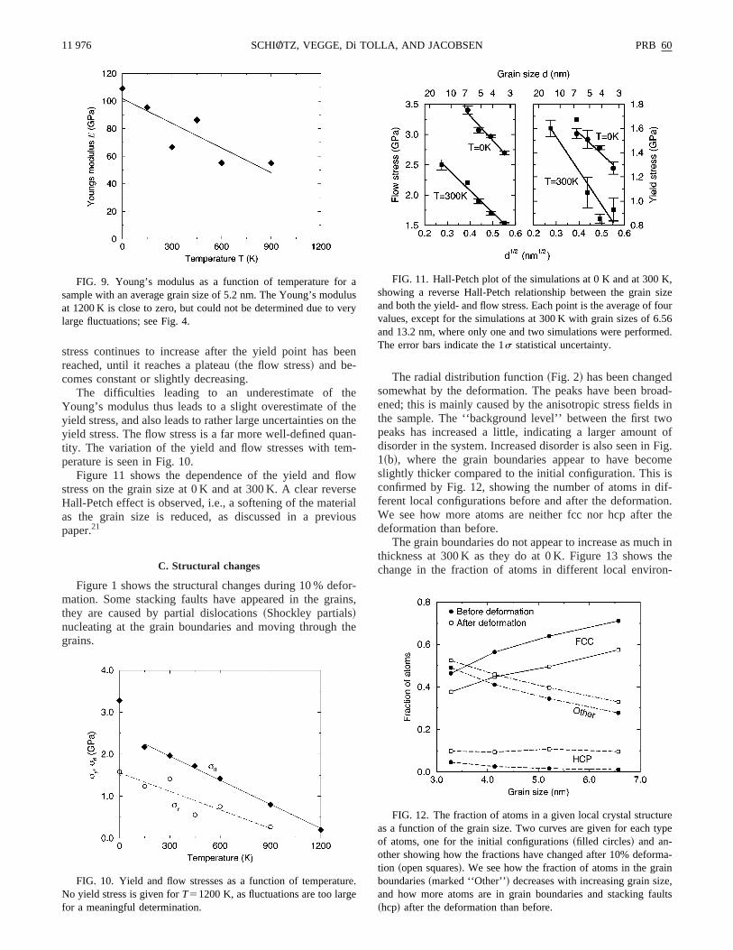
The radial distribution function~Fig. 2! has been changesomewhat by the deformation. The peaks have been brened; this is mainly caused by the anisotropic stress fieldthe sample. The ‘‘background level’’ between the first twpeaks has increased a little, indicating a larger amoundisorder in the system. Increased disorder is also seen in1~b!, where the grain boundaries appear to have becoslightly thicker compared to the initial configuration. Thisconfirmed by Fig. 12, showing the number of atoms in dferent local configurations before and after the deformatiWe see how more atoms are neither fcc nor hcp afterdeformation than before.
The grain boundaries do not appear to increase as mucthickness at 300 K as they do at 0 K. Figure 13 showschange in the fraction of atoms in different local enviro
sry
.
FIG. 11. Hall-Petch plot of the simulations at 0 K and at 300 K,showing a reverse Hall-Petch relationship between the grainand both the yield- and flow stress. Each point is the average ofvalues, except for the simulations at 300 K with grain sizes of 6and 13.2 nm, where only one and two simulations were performThe error bars indicate the 1s statistical uncertainty.
FIG. 12. The fraction of atoms in a given local crystal structuas a function of the grain size. Two curves are given for each tof atoms, one for the initial configurations~filled circles! and an-other showing how the fractions have changed after 10% defortion ~open squares!. We see how the fraction of atoms in the graboundaries~marked ‘‘Other’’! decreases with increasing grain sizand how more atoms are in grain boundaries and stacking fa~hcp! after the deformation than before.

anth
ern
ro
orsarais
sm
b
ab
s
us
s
t
, w
rsain
or-g to
vedx-the
rma-ioncallyof at it
ted
ofn14,e
ain,es.zero
heu-
l-sticeryrma-
per
theund.wesing
e is
trainim-
of
the
de-
s-lehentemas
onat
caa
PRB 60 11 977ATOMIC-SCALE SIMULATIONS OF THE MECHANICAL . . .
ments during the deformation of the same system at 0 Kat 300 K. In both cases we clearly see an increase innumber of hcp atoms~stacking faults! due to the motion ofdislocations through the grains. We also see an increasthe number of atoms in the grain boundaries, in particula0 K. The increase appears to be caused by the deformatiothe grain boundaries. Apparently, the local disorder intduced in this way is partially annealed out at 300 K.
The number of atoms near stacking faults~atoms in hcpsymmetry! is also seen to increase strongly during the defmation ~Figs. 1, 12, and 13!. The stacking faults appear apartial dislocations move through the system, and theythus the signature of dislocation activity. At zero tempeture, we do not observe cases where a second partial dcation erases the stacking faults~we observe only a very fewatoms changing from local hcp order to local fcc order!. Wecan therefore use the total number of hcp-ordered atomestimate an upper bound on the amount of plastic defortion caused by the dislocations.
If a dislocation with Burgers vectorbW runs through theentire system, the dimensions of the system are changedbW
and the strain«zz is thusbzLz21 , wherebz is thez component
of the Burgers vector andLz is the dimension of the systemin the z direction. If the dislocation only passes throughpart of the system, the resulting deformation is reducedA cosf (LxLy)
21, whereA is the area of the slip,Lx andLyare the lateral dimensions of the system, andf is the anglebetween the slip plane and thexy plane. The contributionfrom a slip plane to thezz component of the strain is thu«zz5(bzLz
21)A cosf (LxLy)21.
The maximal value ofbz is b sinf, whereb5ubW u, sincebWlies in the slip plane. The maximal strain from the slip thbecomes«max5bA(2V)215aA(2A6V)21 for f5p/4, asthe Burgers vector of a Shockley partial isb5a/A6, whereais the lattice constant andV is the volume of the simulationcell. A slip plane of areaA results in two$111% planes of hcpatoms, i.e., 4A(A3a2)21 atoms. The total system contain4Va23 atoms, so the fraction of hcp atoms becomesn5Aa(A6V)21. Hence a fractionn of hcp atoms can at moshave resulted in a strain of«max5223/2n. As the simulationgenerate at most 9% hcp atoms during 10% deformation
FIG. 13. Development of the number of atoms in different loenvironments as a function of the strain, for a single simulation0 K and at 300 K.
de
ofatin-
-
re-lo-
toa-
y
y
e
get that«max'3%, provided that all slip planes and Burgevectors are ideally aligned. It is therefore clear that the mdeformation mode is not by dislocation motion.
Figures 14 and 15 illustrate how the main part of defmation has taken place. The atoms are colored accordintheir motionrelative to the global stretching of the system.We clearly see that the upper parts of the grains have modown and the lower parts up, relative to what would be epected in a homogeneous deformation. This shows thatgrains do not stretch as much as in a homogeneous defotion. On the other hand, it is seen that significant deformathas happened in the grain boundaries, as the atoms typiare moving up on one side and down on the other sidegrain boundary. An analysis of that deformation shows thais in the form of a large number of apparently uncorrelasmall slipping events, where a few atoms~or a few tens ofatoms! move relatively to reach other,21 i.e., not in the formof collective motion in the grain boundaries. A minor partthe plastic deformation is in the form of dislocation motioinside the grains. The slip planes are clearly seen in Fig.in particular in the large grain in the upper left part of thfigure, where two dislocations have moved through the grand a third is on its way near one of the previous slip planThe main deformation mode appears to be the same atand at finite temperatures.
D. Strain rate
As the time scale of molecular dynamics is set by tatomic motion, only very brief periods of time can be simlated. For the size of systems discussed here 1 ns~200 000time steps! is for all practical purposes an upper limit, athough for repeated simulations 0.1 ns is a more realilimit. One consequence of the short time scale is that vhigh strain rates are required to get any reasonable defotion within the available time
The finite-temperature simulations presented in this pawere performed at a strain rate of«553108 s21, unlessotherwise is stated. This is very high, but still the ends ofsystem separates at velocities far below the speed of so
In order to investigate the influence of the strain rate,simulated the same deformation of the same system udifferent strain rates in the range 2.53107 s21 – 1.031010
s21; see Fig. 16. A strong dependence on the strain ratseen for strain rates above 13109 s21. Below this ‘‘criticalstrain rate’’ the strain rate dependence on the stress-scurves is far less pronounced. Figure 17 confirms thispression. It shows the yield and flow stress as a functionthe strain rate. Experiments on ultrafine-grained (d'300nm! Cu and Ni show a clear strain rate dependence onyield and flow stresses at high strain rates.57
Perhaps surprisingly, the Young’s modulus appears topend on the strain rate as well~Fig. 16!. This indicates thatsome kind of plastic deformation occurs in the ‘‘linear elatic’’ region. This is confirmed by stopping a simulation whithe system still appears to be in the elastic region, and tallowing it to contract until the stresses are zero. The sysdoes not regain the original length: plastic deformation hoccurred.
To examine the time scale over which this deformatioccurs, a configuration was extracted from the simulation
lt

saa
w far.owers theeenugharly
or-of
ain
11 978 PRB 60SCHIO”TZ, VEGGE, Di TOLLA, AND JACOBSEN
FIG. 14. ~Color! The same system as in Fig. 1~b!, but with theatoms colors according to their motionrelative to the homogeneoudeformation. Blue atoms have moved downwards relative to whwould be expected if the deformation had been homogeneouselastic; red atoms have moved upwards. The scale indicates hothe atoms have moved~in angstroms! during the 10% deformationThe grains are seen to be blue in the upper part, and red in the lpart, indicating that the grains have not been strained as much asystem. This indicates that a major part of the deformation has bin the grain boundaries. Several dislocations have moved throthe large grain in the upper-left corner. Their slip planes are cleseen.
tnd
FIG. 15. ~Color! The same system as in Fig. 14, but after defmation at 300 K; see the caption of that figure for a descriptionthe color coding. The main deformation is seen to be in the grboundaries, as was the case at 0 K.
he same
n.
FIG. 16. ~Color! The effect of varying the strain rate. Stress-strain curves are shown for simulations of the same system at t
temperature~300 K!, but with varying strain rates. A strong influence of strain rate is seen for strain rates above«5109 s21; below that valuethe strain rate dependence is less pronounced. The simulations at the two lowest strain rates were stopped after 4% deformatio

asn
che
enfosrine
ysit
wla
tr
al
i-ed
laredllyve a
ant aro-anzero
e.
nsnareveera-nalns.inguchta-for-e acalan-ess.for-
ex-
ni-eddyre-the
thtra
r-
timh
re.in5.2
PRB 60 11 979ATOMIC-SCALE SIMULATIONS OF THE MECHANICAL . . .
«52.53107 s21 after 0.4% deformation. The system wheld at a fixed length for 300 ps while the stress was motored; see Fig. 18. The stress is seen to decrease with aacteristic time of approximately 100 ps. By plotting thatomic motion in a plot similar to Figs. 14 and 15, it is sethat the relaxation is due to small amounts of plastic demation in the grain boundaries. The consequence of this ithat the systems do not have time to relax completely duthe simulations, explaining the observed strain rate depdence. In order to allow for complete relaxation of the stems, strain rates far below what is practically possible wMD simulations are required.
As another consequence of the short time-scale, sloprocesses will not be seen in the simulations. In particumost diffusional processes will be unobservable~this wouldalso be the case in experiments performed at these high srates!. However, measurements of diffusional creep~Coblecreep! in nanocrystalline metals indicate that diffusioncreep is not a large effect.58,59
TheT50 K simulations were performed using a minimzation procedure. In such simulations time is not defin
FIG. 17. Summary of the effect of varying the strain rate. Bothe yield stress and the flow stress are seen to vary with the s
rate («), strongest for«.109 s21.
FIG. 18. Sample relaxation in the ‘‘elastic’’ region. The defo
mation is stopped after 0.4% deformation at«52.53107 s21 andT5300 K. The stress is seen to decrease with a characteristicof ;100 ps, stabilizing on a value of 2/3 the original stress. Tthick black line is an exponential fit.
i-ar-
r-
gn--h
err,
ain
,
since we are not solving an equation of motion. In a simiway, time should not be relevant in an experiment performtruly at zero temperature, since there will be no thermaactivated processes, and thus no way the sample can lealocal energy minimum. So the strain rate will not haveeffect on the results, providing it is low enough to prevenheating of the sample, and providing the minimization pcedure is fully converged. The minimization simulations cthus be seen as a model for idealized experiments attemperature in the low strain rate limit, where there is timfor the heat generated by the deformation to be removed
E. Grain rotation
Grain rotation has previously been reported in simulatioof nanocrystalline nickel.17 We have investigated the rotatioof the grains during some of the simulations, the resultssummarized in Fig. 19. The figure shows the rotation of firandomly selected grains as a function of strain and tempture. The rotations were identified by a three-dimensioFourier transform of the positions of the atoms in the grai
We see that the grain rotation increases with increastemperature. There is a large variation between how mthe individual grains rotate. The grains with the largest rotions keep the same axis of rotation during the entire demation, whereas the grains that only rotate a little havvarying axis of rotation. Probably some grains are in a loenvironment where a significant rotation results in an advtageous deformation of the sample which reduces the strOther grains are randomly rotated as the many small demation processes in the grain boundaries occur.
F. Porosity
As the observed reverse Hall-Petch effect is oftenplained as an artifact of sample porosity~see Sec. V B!, wefound it relevant to study how pores influence the mechacal properties. The void structure in experimentally producsamples is usually not well known, so we chose to stuseveral different types of voids. In all cases the voidssulted in a reduction of both the Young’s modulus andflow stress; see Fig. 20.
in
ee
FIG. 19. Grain rotation as a function of strain and temperatuThe rotation of five randomly selected grains were followedsimulations at different temperatures. The average grain size isnm. The error bars indicate the 1s spread in the rotations.

yis
lin
-fieuly
es
henatna
-t
m
d-re-es.ials’s
theren-ain
’sd toal:ic
is
u-enl-
s.ent,i-
tionby
of
lusingtly
hesetod-
as
rva-
y onmplerse
theble tor ofall
thesitiesthe
ain
ithine-
r
11 980 PRB 60SCHIO”TZ, VEGGE, Di TOLLA, AND JACOBSEN
Elliptical voids. These cracklike voids were created bremoving all atoms within an oblate ellipsoid with an axratio of 3.16. The short axis can be oriented along the puldirection~the crack is in thexy plane! or perpendicular to it~the crack is in theyz axis!. The former orientation corresponds to cracks that are activated by the applied stressthe effect of these cracks is therefore expected to be mlarger than the effect of the ‘‘inactive’’ cracks. This is clearseen in Fig. 20.
Missing grains.There have been reports of pore sizcomparable to~and proportional to! the grain size.60,61 Tomimic this, we have tried to remove whole grains from tsystem. As the grains are approximately equiaxed, it issurprising that the effect of removing a grain is intermedibetween the effects of removing ellipsoids in the two orietations, provided that approximately the same number ofoms are removed.
Missing grain-boundary atoms.In samples experimentally produced by compacting a powder, it is reasonableassume that the porosity will mainly be in the form of~pos-sibly gas-filled! voids between the grains. There is also so
FIG. 20. Effect of voids on the Young’s modulus~top! and onthe flow stress~bottom!, showing a decrease of both quantities wincreasing void fraction. The voids were generated by removselected atoms, the ‘‘void fraction’’ is the fraction of atoms rmoved. Different methods were used to select the atoms to bemoved; see Sec. IV F.
g
ld,ch
ote-t-
o
e
experimental evidence that this is indeed the case.61,62 Tomimic this, we have removed all atoms in the grain bounaries within one or nine spherical regions in the sample, cating one large or nine small voids in the grain boundariThis type of voids have the largest effect on the materproperties, giving a reduction of 35–40% in the Youngmodulus and flow stress for a 12.5% porosity. It seems ranatural that a large effect is obtained with the voids conctrated in the grain boundaries since we know that the mpart of the deformation is carried by these boundaries.
V. DISCUSSION
A. Elastic properties
From our simulations we get values of the Youngmodulus around 100 GPa at 0 K. This should be comparethe value found for single crystals using this potenti150 GPa at 0 K~Hill average calculated from the anisotropelastic constantsC115173 GPa, C125116 GPa, C44591GPa!. The experimental value for macrocrystalline copper124 GPa at 300 K.63 A significant reduction of the Young’smodulus is thus seen in the nanocrystalline phase.
A similar reduction of Young’s modulus is seen in simlations of nanocrystalline metals grown from a moltphase.11 The low value is usually explained by a large voume fraction of the atoms being in the grain boundarie64
These atoms experience a different atomic environmwhich could result in a reduction of the elastic moduli simlar to what is seen in amorphous metals. This local reducof the elastic constants in grain boundaries is confirmedatomistic simulations.65
Experimental measurements of the Young’s modulushigh quality ~i.e., low-porosity! samples of nanocrystallinecopper and palladium show a reduction in Young’s moduof at most a few percent when correcting for the remainporosity.60 These results were obtained for significanlarger grain sizes than were used in the simulations. Treduction of Young’s modulus that we observe in thesimulations will be difficult to detect experimentally, duethe much lower volume fraction of atoms in the grain bounaries for typical grain sizes in high quality samples (*20nm!.
B. Reverse Hall-Petch effect
A reverse Hall-Petch effect in nanocrystalline copper wfirst observed in nanocrystalline Cu and Pd by Chokshiet al.in 1989.31 Since then, there have been numerous obsetions of softening at very small grain sizes.32–34
The reverse Hall-Petch effect seems to depend stronglthe sample preparation technique used and on the sahistory, perhaps indicating that in most cases the reveHall-Petch effect is caused by various kinds of defects insamples. Surface defects alone have been shown to be adecrease the strength of nanocrystalline metals by a facto5,58,66 and recent studies have shown that even very smamounts of porosity can have a dramatic effect onstrength.60,67 Improved inert gas condensation technique68
have reduced the porosity resulting in samples with densabove 98% of the fully dense value. In these samplesordinary Hall-Petch effect is seen to continue down to gr
g
e-

warnsedhrenas
thmhn
b
thlotio
f
re
aninw
e
anemintots
or
iselbso-
ll-ndug
sliath
iet
dd
ecall
thi
earities,dis-en
ca-ex-inef-u-e inheis
eenno-
sticthees.ar-mse
riesum-s to
rentalinatesrainas-
ex-
theceduldon-r ofoft-for
it
sh
ishnteran-
PRB 60 11 981ATOMIC-SCALE SIMULATIONS OF THE MECHANICAL . . .
sizes around 15 nm.60 There are only few data points belothat grain size, but apparently no further increase in the hness is seen. It is suggested that most of the observatioa reverse Hall-Petch effect in nanocrystalline metals arresult of poor sample quality.60 This impression is supporteby literature studies32,69indicating that the reverse Hall-Petceffect is mainly seen when the grain size is varied bypeated annealing of a single sample, whereas an ordiHall-Petch relationship is seen when as-prepared sampleused.
However, there does seem to be a deviation fromHall-Petch effect for grain sizes below approximately 15 nwhere the Hall-Petch slope is seen to decrease or vanissamples produced with various techniques. This is seeCu samples produced by inert gas condensation followedwarm compaction~sample densities above 98%! ~Ref. 60!and in electroplated Ni~claimed to be porosity free!.70,71
There are theoretical arguments for expecting thatHall-Petch relation ceases to be valid for grain sizes be;20 nm: as the grain size becomes too small, dislocapileups are no longer possible, and the usual explanationHall-Petch behavior does not apply.59,72,73
Many models have been proposed to explain why averse Hall-Petch effect is sometimes seen. Chokshiet al.31
proposed that enhanced Coble creep, i.e., creep by vacdiffusion in the grain boundaries, should result in a softenat the smallest grain sizes as the creep rate increasesdecreasing grain size~d! asd23. Direct measurements of thcreep rate have however ruled this out.59,74
It has been suggested that the grain boundaries in ncrystalline metals have a different structure, making thmore transparent to dislocations than ‘‘ordinary’’ graboundaries.75–77If it becomes possible for the dislocationsrun through several grains as the grain size is reduced,Hall-Petch relations would break down. In our simulationwe have not observed dislocations moving through mthan one grain.
If the Hall-Petch effect is explained by appealing to dlocation sources in the grain boundaries, the Hall-Petch rtionship is expected to break down when the grain sizescomes so low that there are no longer dislocation sourceall grain boundaries78 ~assuming a constant density of dislcation sources in the grain boundaries!.
Hahn and co-workers79,80 suggest that the reverse HaPetch effect is caused by deformation in the grain bouaries. If a grain boundary slides, stress concentrations bup where the grain boundary ends, limiting further slidinSubstantial sliding on a macroscopic scale occurs whening occurs on slide planes consisting of many aligned grboundaries; the sliding is hindered by the roughness ofslide plane due to its consisting of many grain boundarAs the grain size is reduced and becomes comparable tograin-boundary width, the roughness of such slide planescreases and the stress required for mesoscopic slidingcreases. This would result in a reverse Hall-Petch effThey estimate the transition from normal to reverse HPetch effect to occur at grain sizes near 50 nm for Cu.79
The simulations reported in the present paper indicatethe main deformation mechanism at these grain sizes is
d-ofa
-ry
are
e,ininy
ewnor
-
cygith
o-
he,e
-a-e-in
-ild.d-ine
s.hee-e-t.-
atn-
deed sliding in the grain boundaries. However, it is not clif the proposed ‘‘collective’’ sliding events are occurring,appears that sliding occurs on individual grain boundarand that the resulting stress buildup is relieved throughlocation motion in the grains. There is a competition betwethe ordinary deformation mode~dislocations! and the grain-boundary sliding. As the grain size is increased, the dislotion motion is eventually expected to dominate, and wepect a transition to a behavior more like what is seencoarse-grained materials, including a normal Hall-Petchfect. The transition is beyond what can currently be simlated at the atomic scale, but we do see a weak increasthe dislocation activity when the grain size is increased: Tincrease in the fraction of hcp atoms during a simulationincreasing slightly with the grain size~Fig. 12!.
VI. CONCLUSIONS
Molecular dynamics and related techniques have bshown to be a useful approach to study the behavior of nacrystalline metals. We have in detail investigated the pladeformation of nanocrystalline copper, and shown thatmain deformation mode is sliding in the grain boundariThe sliding happens through a large number of small, appently uncorrelated events, where a few grain boundary ato~or a few tens of atoms! move past each other. It remains thmain deformation mechanism at all grain sizes studied~up to13 nm!, even at zero temperature. As the grain boundaare the main carriers of the deformation, decreasing the nber of grain boundaries by increasing the grain size leada hardening of the material; areverse Hall-Petch effect. Thisis observed in the simulations, both forT50 K and for T5300 K.
The Young’s moduli of the nanocrystalline systems afound to be reduced somewhat compared to the experimevalue for polycrystalline copper with macroscopic grasizes, decreasing with decreasing grain size. This indicthat the grain boundaries are elastically softer than the ginteriors. The Young’s modulus is decreasing with increing temperature at a rate somewhat above what is seenperimentally in coarser-grained copper.
Pores in the samples have a large effect on bothYoung’s modulus and the flow stress. This effect is enhanif the pores are mainly in the grain boundaries, as one coexpect in samples produced experimentally by inert gas cdensation. Sample porosity can explain a large numbeexperiments showing reverse Hall-Petch effect, but the sening due to grain boundary sliding may be importanthigh-quality samples with grain sizes close to the lower limof what can be reached experimentally.
ACKNOWLEDGMENTS
Major parts of this work were financed by The DaniTechnical Research Council~STVF! through Grant No.9601119. Parallel computer time was financed by the DanResearch Councils through Grant No. 9501775. The Cefor Atomic-scale Materials Physics is sponsored by the Dish National Research Council.

ra
rig
p,
ey
rse
S.
d R
s
r.
.ed6
.
R
ini-aln
.ed
9
R.
ll.
cr.
.
no-
-
tat.
J. K.
n-
D.
, J.
ice,’’s are
11 982 PRB 60SCHIO”TZ, VEGGE, Di TOLLA, AND JACOBSEN
*Also at: Materials Research Department, Risø National Labotory, DK-4000 Roskilde, Denmark.
†Present address: INFM and SISSA, Via Beirut 2-4, I-34014 Gnano~TS!, Italy.1F. F. Abraham, Europhys. Lett.38, 103 ~1997!.2V. Bulatov, F. F. Abraham, L. Kubin, B. Devincre, and S. Yi
Nature~London! 391, 669 ~1998!.3S. J. Zhou, D. L. Preston, P. S. Lomdahl, and D. M. Beazl
Science279, 1525~1998!.4T. Rasmussen, K. W. Jacobsen, T. Leffers, and O. B. Pede
Phys. Rev. B56, 2977~1997!.5T. Rasmussen, K. W. Jacobsen, T. Letters, O. B. Pedersen,
Srinivasan, and H. Jo´nsson, Phys. Rev. Lett.79, 3676~1997!.6 R. W. Siegel and G. E. Fougere, inNanophase Materials:
Synthesis—Properties—Applications, Vol. 260 of NATO-ASISeries E: Applied Sciences, edited by G. C. Hadjipanayis anW. Siegel~Kluwer, Dordrecht, 1994!, pp. 233–261.
7R. W. Siegel, Mater. Sci. Forum235-238, 851 ~1997!.8D. G. Morris and M. A. Morris, Mater. Sci. Forum235-238, 861
~1997!.9 D. G. Morris,Mechanical Behavior of Nanostructured Material,
Vol. 2 of Materials Science Foundations~Trans Tech Publica-tions, Utikon-Zurich, 1998!.
10D. Chen, Comput. Mater. Sci.3, 327 ~1995!.11S. R. Phillpot, D. Wolf, and H. Gleiter, J. Appl. Phys.78, 847
~1995!.12S. R. Phillpot, D. Wolf, and H. Gleiter, Scr. Metall. Mater.33,
1245 ~1995!.13H. Zhu and R. S. Averback, Mater. Manuf. Processes11, 905
~1996!.14P. Keblinski, R. Phillpot, D. Wolf, and H. Gleiter, Acta Mate
45, 987 ~1997!.15 G. D’Agostino and H. Van Swygenhoven, inMetastable Phases
and Microstructures, edited by R. Borman, G. Mazzone, R. DShull, R. S. Averback, and R. F. Ziolo, MRS Symposia Proceings No. 400~Materials Research Society, Pittsburgh, 199!,p. 293.
16H. Van Swygenhoven and A. Caro, Appl. Phys. Lett.71, 1652~1997!.
17H. Van Swygenhoven and A. Caro, Nanostruct. Mater.9, 669~1997!.
18H. Van Swygenhoven and A. Caro, Phys. Rev. B58, 11 246~1998!.
19H. Van Swygenhoven, M. Spacze´r, and A. Caro, NanostructMater.10, 819 ~1998!.
20 H. Van Swygenhoven, M. Spacze´r, and A. Caro, inMicroscopicSimulation of Interfacial Phenomena in Solids and Liquids, ed-ited by S. R. Phillpot, P. D. Bristowe, D. G. Stroud, and J.Smith, MRS Symposia Proceedings No. 492~Materials Re-search Society, Pittsburgh, 1998!, pp. 357-362.
21J. Schiøtz, F. D. Di Tolla, and K. W. Jacobsen, Nature~London!391, 561 ~1998!.
22 J. Schiøtz, T. Vegge, F. D. Di Tolla, and K. W. Jacobsen,Modelling of Structure and Mechanics of Materials from Mcroscale to Product, Proceedings of the 19th Risø InternationSymposium on Materials Science, edited by J. V. Carstenseet al. ~Risø National Laboratory, Roskilde, 1998!, pp. 133–148.
23 J. Schiøtz, T. Vegge, and K. W. Jacobsen, inMultiscale Model-ing of Materials, edited by V. Bulatov, T. D. de la Rubia, RPhillips, E. Kaxiras, and N. Ghoniem, MRS Symposia Proce
-
-
,
n,
G.
.
-
.
-
ings No. 538~Materials Research Society, Pittsburgh, 199!,p. 299.
24J. R. Weertman, D. Farkas, K. Hemker, H. Kung, M. Mayo,Mitra, and H. Van Swygenhoven, MRS Bull.24, 44 ~1999!.
25E. O. Hall, Proc. Phys. Soc. London, Sect. B64, 747 ~1951!.26N. J. Petch, J. Iron Steel Inst., London174, 25 ~1953!.27J. C. M. Li and Y. T. Chou, Metall. Trans. A1, 1145~1970!.28Z. Jiang, J. Lian, and B. Baudelet, Acta Metall. Mater.43, 3349
~1995!.29L. H. Friedman and D. C. Chrzan, Phys. Rev. Lett.81, 2715
~1998!.30L. H. Friedman and D. C. Chrzan, Philos. Mag. A77, 1185
~1998!.31A. H. Chokshi, A. Rosen, J. Karch, and H. Gleiter, Scr. Meta
23, 1679~1989!.32G. E. Fougere, J. R. Weertman, R. W. Siegel, and S. Kim, S
Metall. Mater.26, 1879~1992!.33T. R. Malow, C. C. Koch, P. Q. Miraglia, and K. L. Murty, Mater
Sci. Eng., A252, 36 ~1998!.34T. Yamasaki, P. Schloßmacher, K. Ehrlich, and Y. Ogino, Na
struct. Mater.10, 375 ~1998!.35R. W. Siegel, J. Phys. Chem. Solids55, 1097~1994!.36H. Natter, M. Schmelzer, and R. Hempelmann, J. Mater. Res.13,
1186 ~1998!.37 A. Okabe, B. Boots, and K. Sugihara,Spatial Tesselations: Con
cepts and Applications of Voronoi Diagrams~Wiley, Chichester,1992!.
38S. Kumar, S. K. Kurtz, J. R. Banavar, and M. G. Sharma, J. SPhys.67, 523 ~1992!.
39O. H. Nielsen, J. P. Sethna, P. Stoltze, K. W. Jacobsen, andNørskov, Europhys. Lett.26, 51 ~1994!.
40 J. Schiøtz, Ph.D. thesis, Technical University of Denmark, Lygby, Denmark, 1995.
41E. A. Stern, R. W. Siegel, M. Newville, P. G. Sanders, andHaskel, Phys. Rev. Lett.75, 3874~1995!.
42K. W. Jacobsen, J. K. Nørskov, and M. J. Puska, Phys. Rev. B35,7423 ~1987!.
43K. W. Jacobsen, P. Stoltze, and J. K. Nørskov, Surf. Sci.366, 394~1996!.
44 M. P. Allen and D. J. Tildesley,Computer Simulation of Liquids~Claredon Press, Oxford, 1987!.
45W. C. Swope, H. C. Andersen, P. H. Berens, and K. R. WilsonChem. Phys.76, 637 ~1982!.
46 In order to implement periodic boundary conditions all atomcoordinates are internally represented in a ‘‘scaled spacwhere coordinates are between 0 and 1. The real coordinateobtained by multiplying with a matrixM. The system is de-formed by changing the relevant components ofM, not bychanging the scaled-space coordinates.
47 The minimization method is described under the nameMolecularDynamics Minimizationin P. Stoltze,Simulation Methods inAtomic Scale Materials Physics~Polyteknisk Forlag, Lyngby,Denmark, 1997!.
48T. Egami, K. Maede, and V. Vitek, Philos. Mag. A41, 883~1980!.
49J. R. Ray and A. Rahman, J. Chem. Phys.80, 4423~1984!.50J. R. Ray and A. Rahman, J. Chem. Phys.82, 4243~1985!.51D. H. Tsai, J. Chem. Phys.70, 1375~1979!.52J. F. Lutsko, J. Appl. Phys.64, 1152~1988!.53K. S. Cheung and S. Yip, J. Appl. Phys.70, 5688~1991!.54H. Jonsson and H. C. Andersen, Phys. Rev. Lett.60, 2295~1988!.

e
S
at
f
er
l.
at
, a
of
si,
ll.
A
uct.
r.
all.
B.
ter.
PRB 60 11 983ATOMIC-SCALE SIMULATIONS OF THE MECHANICAL . . .
55A. S. Clarke and H. Jo´nsson, Phys. Rev. E47, 3975~1993!.56A. B. Lebedevet al., Mater. Sci. Eng., A203, 165 ~1995!.57G. T. Gray III et al., Nanostruct. Mater.9, 477 ~1997!.58G. W. Nieman, J. R. Weertman, and R. W. Siegel, J. Mater. R
6, 1012~1991!.59T. G. Nieh and J. Wadsworth, Scr. Metall. Mater.25, 955~1991!.60P. G. Sanders, C. J. Youngdahl, and J. R. Weertman, Mater.
Eng., A 234-236, 77 ~1997!.61P. G. Sanders, J. A. Eastman, and J. R. Weertman, Acta M
46, 4195~1998!.62 S. R. Agnewet al., in Modelling of Structure and Mechanics o
Materials from Microscale to Product, Proceedings of the 19thRisø International Symposium on Materials Science, edited by J.V. Carstensenet al. ~Risø National Laboratory, Roskilde, 1998!,pp. 1–14.
63K. A. Gschneidner, Solid State Phys.16, 275 ~1964!.64T. D. Shen, C. C. Koch, T. Y. Tsui, and G. M. Pharr, J. Mat
Res.10, 2892~1995!.65M. D. Kluge, D. Wolf, J. F. Lutsko, and S. R. Phillpot, J. App
Phys.67, 2370~1990!.66J. R. Weertman, Mater. Sci. Eng., A166, 161 ~1993!.67P. G. Sanders, J. A. Eastman, and J. R. Weertman, Acta M
45, 4019~1997!.68P. G. Sanders, G. E. Fougere, L. J. Thompson, J. A. Eastman
J. R. Weertman, Nanostruct. Mater.8, 243 ~1997!.69 J. Grilhe, inMechanical Properties and Deformation Behavior
s.
ci.
er.
.
er.
nd
Materials Having Ultra-Fine Microstructures, Vol. 233 ofNATO-ASI Series E: Applied Sciences, edited by M. NastaD. M. Parker, and H. Gleiter~Kluwer, Dordrecht, 1993!, pp.255–286.
70A. M. El-Sherik, U. Erb, G. Palumbo, and K. T. Aust, Scr. MetaMater.27, 1185~1992!.
71N. Wang, Z. Wang, K. T. Aust, and U. Erb, Mater. Sci. Eng.,237, 150 ~1997!.
72C. S. Pande, R. A. Masumura, and R. W. Armstrong, NanostrMater.2, 323 ~1993!.
73N. Wang, Z. Wang, K. T. Aust, and U. Erb, Acta Metall. Mate43, 519 ~1995!.
74G. W. Nieman, J. R. Weertman, and R. W. Siegel, Scr. MetMater.24, 145 ~1990!.
75R. Z. Valiev, F. Chmelik, F. Bordeaux, G. Kapelski, andBaudelet, Scr. Metall. Mater.27, 855 ~1992!.
76J. Lian, B. Baudelet, and A. A. Nazarov, Mater. Sci. Eng., A172,23 ~1993!.
77K. Lu and M. L. Sui, Scr. Metall. Mater.28, 1465~1993!.78 S. Li, L. Sun, and Z. Wang, inStrength of Materials, edited by
H. Oikawa, K. Maruyama, S. Takeuchi, and M. Yamaguchi~TheJapan Institute of Metals, 1994!, pp. 873–876.
79H. Hahn and K. A. Padmanabhan, Philos. Mag. B76, 559~1997!.80H. Hahn, P. Mondal, and K. A. Padmanabhan, Nanostruct. Ma
9, 603 ~1997!.