Array Allocation Taking into Account SDRAM Characteristics Hong-Kai Chang Youn-Long Lin Department...
22
Array Allocation Taking into Account SDRAM Characteristics Hong-Kai Chang Youn-Long Lin Department of Computer Science National Tsing Hua University HsinChu, Taiwan, R.O.C.
-
date post
21-Dec-2015 -
Category
Documents
-
view
219 -
download
1
Transcript of Array Allocation Taking into Account SDRAM Characteristics Hong-Kai Chang Youn-Long Lin Department...

Array Allocation Taking into Account SDRAM Characteristics
Hong-Kai ChangYoun-Long LinDepartment of Computer ScienceNational Tsing Hua UniversityHsinChu, Taiwan, R.O.C.

2
Outline
IntroductionRelated WorkMotivationSolving ProblemProposed AlgorithmsExperimental ResultsConclusions and Future Work

3
Introduction
Performance gap between memory and processor
Systems without cache Application specific Embedded DRAM
Optimize DRAM performance by utilize its special characteristics
SDRAM’s multi-bank architecture enables new optimizations in scheduling
We assign arrays to different SDRAM banks to increase data access rate

4
Related Work
Previous research eliminate memory bottleneck by Using local memory (cache) Prefetch data as fast as possible
Panda, Dutt, and Nicolau utilizing page mode access to improve scheduling using EDO DRAM
Research about array mapping to physical memories for low power, lower cost, better performance

5
Motivation
DRAM operations Row decode Column decode Precharge
SDRAM characteristics Multiple banks Burst transfer Synchronous
Traditional DRAM 2-bank SDRAM
Row
Column
Row
Column
B a n k 1B a n k 0

6
Address Mapping Table
Host Address: [a16:a0] Memory Address: [BA, A7-A0]
Page Size for host: Page Size for DRAM:
128 words (a6:a0) 256 words (A7:A0)
-If we exchange the mapping of a0 and a7...
BA A7 A6 A5 A4 A3 A2 A1 A0Row a7 a16 a15 a14 a13 a12 a11 a10 a99x8Col a8 a6 a5 a4 a3 a2 a1 a0
A 9x8 SDRAM address mapping table (Bank interleaving size: 128 words)
BA A7 A6 A5 A4 A3 A2 A1 A0Row a0 a16 a15 a14 a13 a12 a11 a10 a99x8Col a8 a6 a5 a4 a3 a2 a1 a7
A 9x8 SDRAM address mapping table (Bank interleaving size: 1 word)

7
Motivational Example
BA=BankActive
=RowDecode
R/W=Read/Write =ColumnDecode
BP=Precharge
BA1
BP1
BP2
BA2
R1 R2
Command Bus (Address Bus)
Data1
Data2
DataBus
BA1
BP1
BP2
BA2
R1 R2
Data3
Data4
27 Cycles
1 2 3 4 5 6 7 8 9 10 11 12 13 14
16 17 18 19 20 21 22 23 24 25 26 27 2815

8
Motivational Example
BA=BankActive
=RowDecode
R/W=Read/Write =ColumnDecode
BP=Precharge
BA1
BP1
BP2
BA2
R1 R2
Command Bus (Address Bus)
Data1
Data2
DataBus
R3 R4
Data3
Data4
10 Cycles1 2 3 4 5 6 7 8 9 10
BA1
BP1
BP2
BA2
R1 R2
Command Bus (Address Bus)
Data1
Data2
DataBus
BA1
BP1
BP2
BA2
R1 R2
Data3
Data4
16 Cycles1 2 3 4 5 6 7 8 9 10 11 12 13 14 15 16

9
Assumptions
Harvard architecture : Separated program/data memory Paging policy of the DRAM controller
Does not perform precharge after read/write If next access reference to different page, perform precharge, foll
owed by bank active, before read/write As many pages can be opened at once as the number of banks
Resource constraints
Function Unit ALU Multiplier Divider SDRAM SDRAMSupported Op +,-,>,S * / BA,BP R,WClocks 1 2 4 2 3Quantity 1 1 1 2 or 4 2 or 4
10
Problem Definition
Input a data flow graph, the resource constraints, and the memory configuration
Perform our bank allocation algorithm Schedule the operations with a static list scheduling
algorithm considering SDRAM timing constraints Output a schedule of operations, a bank allocation table,
and the total cycle counts

11
Bank Allocation Algorithm
Calculate Node distances Calculate Array distances Give arrays with the shorter distances higher priority Allocate arrays to different banks if possible

12
Example: SOR
main(){ float a[N][N], b[N][N], C[N][N], d[N][N], e[N][N], f[N][N]; float omega, resid, u[N][N]; int j,l;
for (j=2; j<N; j++) for (l=1;l<N;l+=2) { resid = a[j][l]*u[j+1][l]+ b[j][l]*u[j-1][l]+ c[j][l]*u[j][l+1]+ d[j][l]*u[j][l-1]+ e[j][l]*u[j][l] – f[j][l]; u[j][l] -= omega*resid/e[j][l]; }}
RR
*
RR
*
RR
*
RR
*
+
+
+
a
b
c
d
u[j+1][l]
u[j-1][l]
u[j][l+1]
u[j][l-1]
{1,-,-,-,-,-,-,1,-}
{-,1,-,-,-,-,-,-,1}
{2,2,-,-,-,-,-,2,2}
{-,-,1,-,-,-,1,-,-}
{-,-,-,1,-,-,1,-,-}
{-,-,2,2,-,-,2,-,-}
{3,3,3,3,-,-,3,3,3}
D F G o f S O R (p a rtia l)

13
Node Distance
Distances between current node and the nearest node that access array a, b, c,…. Shown in { }
Ex. {1,-,-,-,-,-,-,1,-} means the distances to the node that access array a[j] and u[j-1] are both 1.
‘-’ means the distance is still unknown When propagate downstream, the distance increases.
RR
*
RR
*
+
a
b
u[j+1][l]
u[j-1][l]
{1,-,-,-,-,-,-,1,-}
{-,1,-,-,-,-,-,-,1}
{2,2,-,-,-,-,-,2,2}
distance to a[j]
distance to u[j-1]
distance to b[j]

14
Array Distance
The distance between nodes that access arrays Calculate from node distance of corresponding arrays Get the minimum value
Ex. AD(a[j], u[j-1])=min(2,4)=2
RR
*
RR
*
+
a
b
u[j+1][l]
u[j-1][l]
{1,-,-,-,-,-,-,1,-}
{-,1,-,-,-,-,-,-,1}
{2,2,-,-,-,-,-,2,2}
AD(a[j], u[j-1])=1+1=2
AD(a[j], b[j]) =2+2=4
AD(a[j], u[j-1])=2+2=4

15
Example: SOR
a[j] b[j] c[j] d[j] e[j] f[j] u[j] u[j+1] u[j-1]a[j] 0 4 6 6 7 6 6 2 4b[j] 4 0 6 6 7 6 6 4 2c[j] 6 6 0 4 7 6 2 6 6d[j] 6 6 4 0 7 6 2 6 6e[j] 7 7 7 7 0 3 2 7 7f[j] 6 6 6 6 3 0 3 6 6u[j] 6 6 2 2 2 3 0 6 6
u[j+1] 2 4 6 6 7 6 6 0 4u[j-1] 4 2 6 6 7 6 6 4 0
Array distance table of SOR
Bank allocation:
Bank 0: c,d,e,f Bank 1: a,b,u

16
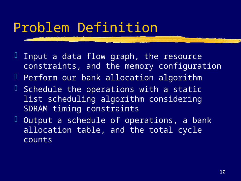
Experimental Characteristics
We divided our benchmarks into two groups First group benchmarks access multiple 1-D arrays
Apply our algorithm to arrays Second group benchmarks access single 2-D arrays
Apply our algorithm to array rows Memory configurations
Multi-bank configuration: 2 banks/ 4banks Multi-chip configuration: 2 chips/ 4chips Multi-chip vs mulit-bank: relieves bus contention Utilizing page mode access or not
17
Results of the first group (multiple array)
0%
10%
20%
30%
40%
50%
60%
70%
80%
90%
100%
dhrc dequant wiener dct mmult leafcomp fir sor
Benchmark
No
rmali
ze
d C
ycle
Coarse 1Bank 2Bank 4Bank 2Chips 4Chips 2Bank+P 4Bank+P 2Chips+P 4Chips+P

18
Results of the second group (single array)
0%
10%
20%
30%
40%
50%
60%
70%
80%
90%
100%
compress laplace sobel lowpass compress2 laplace2 sobel2 lowpass2
Benchmark
No
rmali
ze
d C
ycle
Coarse 1Bank 2Bank 4Bank 2Chips 4Chips 2Bank+P 4Bank+P 2Chips+P 4Chips+P

19
Results compare to Panda's
0%
10%
20%
30%
40%
50%
60%
70%
80%
90%
100%
dhrc dequant mmult leafcomp sor lowpass
Benchmark
No
rmali
ze
d C
ycle
s
Coarse 1Bank 2Bank 4Bank 2Chips 4Chips 2Bank+P 4Bank+P 2Chips+P 4Chips+P Panda

20
Experimental Results
From the average results, we can see that Scheduling using SDRAM with our bank allocation algorithm do
improve the performance Utilizing page mode access relieves the traffic of address bus,
thus the use of multiple chips does not make obvious improvement
Configuration 1 Chip/2 Banks 1 Chip/4 Banks 2 Chips/1 Bank 4 Chips /1 BankW/O PageMode 70.20% 62.28% 64.93% 54.51%W/ PageMode 53.38% 43.36% 52.52% 42.02%
Average schedule length of different configurations

21
Conclusions
We presented a bank allocation algorithm incorporated in our scheduler to take advantages of SDRAM
The scheduling results have a great improvement from the coarse one and beat Panda’s work in some cases
Our work is based on a common paging policy Several different memory configurations are exploited Scheduling results are verified and meet Intel’s PC
SDRAM’s spec

22
Future Works
Extending our research to Rambus DRAM Grouping arrays to incorporating burst transfer Integration with other scheduling /allocation techniq
ues


![Learning Camera-Aware Noise Models - ECVA...Hwann-Tzong Chen2[0000 0003 2806 7090] 1 MediaTek Inc., Hsinchu, Taiwan 2 National Tsing Hua University, Hsinchu, Taiwan Abstract. Modeling](https://static.fdocuments.net/doc/165x107/60fe7bbda948282bed227474/learning-camera-aware-noise-models-ecva-hwann-tzong-chen20000-0003-2806-7090.jpg)