Analysis and Design of High-Speed CMOS Frequency Dividers
87
UC Irvine UC Irvine Electronic Theses and Dissertations Title Analysis and Design of High-Speed CMOS Frequency Dividers Permalink https://escholarship.org/uc/item/9q86n8b2 Author Molainezhad, Fatemehe Publication Date 2015 Copyright Information This work is made available under the terms of a Creative Commons Attribution License, availalbe at https://creativecommons.org/licenses/by/4.0/ Peer reviewed|Thesis/dissertation eScholarship.org Powered by the California Digital Library University of California
Transcript of Analysis and Design of High-Speed CMOS Frequency Dividers
UC IrvineUC Irvine Electronic Theses and Dissertations
TitleAnalysis and Design of High-Speed CMOS Frequency Dividers
Permalinkhttps://escholarship.org/uc/item/9q86n8b2
AuthorMolainezhad, Fatemehe
Publication Date2015
Copyright InformationThis work is made available under the terms of a Creative Commons Attribution License, availalbe at https://creativecommons.org/licenses/by/4.0/ Peer reviewed|Thesis/dissertation
eScholarship.org Powered by the California Digital LibraryUniversity of California

UNIVERSITY OF CALIFORNIA, IRVINE
Analysis and Design of High-Speed CMOS Frequency Dividers
Thesis
submitted in partial satisfaction of the requirements for the degree of
Master
in Electrical & Computer Engineering
by
Fatemehe Molainezhad
Master Thesis Committee:
Professor Michael Green, Chair Professor Payam Heydari
Professor Nader Bagerzadeh
2015

© 2015 Fatemehe Molainezhad

ii
DEDICATION
To my family

iii
TABLE OF CONTENTS
Page LIST OF FIGURES ........................................................................................................................................ v
LIST OF ABBREVIATIONS......................................................................................................................... viii
ACKNOWLEDGMENTS ............................................................................................................................... ix
CURRICULUM VITAE ................................................................................................................................... x
ABSTRACT OF THE THESIS ...................................................................................................................... xi
CHAPTER 1. INTRODUCTION ..................................................................................................................... 1
1.1 Overview ........................................................................................................................................... 1
1.2 Outline .............................................................................................................................................. 3
CHAPTER 2. REVIEW OF PUBLISHED WORK ........................................................................................... 4
2.1 A Study of Injection-Locking and Pulling in Oscillators .................................................................... 4
2.2 Analysis of Nonlinearities in Injection-Locked Frequency Dividers .................................................. 5
2.3 A Study of Locking Phenomena in Oscillators ................................................................................. 7
CHAPTER 3. High Frequency Clock Dividers ............................................................................................. 10
3.1 High-Speed Frequency Divider Based on CML D Flip-Flop........................................................... 10
3.1.1 CML Buffer ............................................................................................................................ 10
3.1.2 CML D Flip-Flop Divider ........................................................................................................ 12
3.1.3 Plotting Sensitivity Curve ....................................................................................................... 15
3.1.4 Procedure to Measure Phase Difference Between Two Signals .......................................... 17
3.1.5 Analyzing Instantaneous Frequency and Phase for DFF Divider ......................................... 18
3.2 High-Speed Frequency Dividers Based on CML Ring ................................................................... 23
3.2.1 Circuit Parameters Design .................................................................................................... 25
3.2.2 CML Ring Frequency Divider's Sensitivity Curve .................................................................. 26
3.2.3 Analyzing Instantaneous Frequency and Phase Shift .......................................................... 28
3.3 High-Speed Frequency Dividers Based on LC-tank Oscillator ...................................................... 31
3.3.1 LC-tank Frequency Divider's Sensitivity Curve ..................................................................... 33
3.3.2 Analyzing Instantaneous Frequency and Phase Shift for LC-tank ........................................ 35
iv
CHAPTER 4. Analyzing Locking Phase ...................................................................................................... 40
4.1 LC-Tank Frequency Dividers .......................................................................................................... 40
4.1.1 Validating Calculation of ϕ by Simulation Results for LC-tank Divider .................................. 47
4.2 CML Ring Frequency Divider ......................................................................................................... 50
4.2.1 Validating Calculation of ϕ by Simulation Results for Ring Divider ....................................... 57
4.3 CML D Flip-Flop Frequency Divider ............................................................................................... 61
4.3.1 Validating Calculation of ϕ by Simulation Results for DFF Divider ....................................... 66
CHAPTER 5. SUMMARY AND CONCLUSIONS ........................................................................................ 71
REFERENCES ............................................................................................................................................ 72

v
LIST OF FIGURES
Page Figure 2-1 (a) Conceptual oscillator, (b) Frequency shift by injection, (c) Open-loop characteristics, and (d) Phase
difference between input and output currents [6]. ........................................................................................ 4
Figure 2-2 (a) Current injection mode of CML-DFF divider, (b) Schematic of new frequency divider [2]. .............. 6
Figure 2-3 (a) Adler's model for oscillator circuit, (b) Vector diagram of instantaneous voltages for oscillator [4]. ... 7
Figure 3-1 (a) CML differential pair [10], (b) Characteristics of a simple CML buffer [9]. ................................... 11
Figure 3-2 Topology of a DFF frequency divider. ............................................................................................. 12
Figure 3-3 CML D Flip-Flop clock divider schematic. ...................................................................................... 13
Figure 3-4 Finding optimum common-mode input voltage for CKP/N inputs. ..................................................... 14
Figure 3-5 Sample of the simulation results for plotting the DFF divider's sensitivity curve.................................. 16
Figure 3-6 Sensitivity curve for the DFF frequency divider. .............................................................................. 17
Figure 3-7 Simulation results for an injected signal and its effect on instantaneous frequency. ............................. 19
Figure 3-8 Simulation results when the clock amplitude is changed for DFF divider. ........................................... 20
Figure 3-9 Simulation results when the clock is applied at different starting times for DFF divider. ...................... 21
Figure 3-10 Transient response due to phase variations of the injection signal for DFF divider. ............................ 22
Figure 3-11 CML ring clock divider schematic. ................................................................................................ 23
Figure 3-12 Realization of single balanced mixer. ............................................................................................ 24
Figure 3-13 Self oscillation frequency for ring divider. ..................................................................................... 26
Figure 3-14 An example of finding two points in the sensitivity curve for Vm=400mV. ....................................... 27
Figure 3-15 Sensitivity curve for 4-stage ring frequency divider. ....................................................................... 27
Figure 3-16 An example of the effect of an injected signal on instantaneous ....................................................... 28
Figure 3-17 Simulation results when the clock amplitude is changed for ring divider. .......................................... 29
Figure 3-18 Simulation results when the clock is applied at different starting times for ring divider. ..................... 30
Figure 3-19 The instantaneous phase due to injection signal for ring divider. ...................................................... 31
Figure 3-20 LC-tank frequency divider schematic. ............................................................................................ 32
Figure 3-21 Self oscillation frequency for LC-tank frequency divider. ................................................................ 33
Figure 3-22 An example to find (FMin-m,Vm) and (FMax-m,Vm) points for the LC-tank divider. ................................ 34

vi
Figure 3-23 Sensitivity curve for LC-tank frequency divider. ............................................................................ 34
Figure 3-24 An injected signal and its effect on LC-tank frequency divider's output. ........................................... 35
Figure 3-25 Simulation results when the clock amplitude is changed for LC-tank divider..................................... 36
Figure 3-26 Simulation results when the clock is applied at different starting times for LC-tank divider. ............... 37
Figure 3-27 Simulation results when the clock amplitude and injection starting times are varied. .......................... 38
Figure 4-1 Schematic of the LC-tank frequency divider with current injected to the tank nodes. ........................... 40
Figure 4-2 (a) Equivalent circuit, (b) Block diagram and (c) Vector representation of LC-tank divider. ................. 41
Figure 4-3 An example of simulation results showing vector representation of the three. ..................................... 41
Figure 4-4 Periodic function that appears in any type of divider. ........................................................................ 42
Figure 4-5 Finding the quality factor. .............................................................................................................. 45
Figure 4-6 Simulation results for LC-tank based frequency divider. ................................................................... 47
Figure 4-7 Simulation results showing the locking frequency and phase for LC-tank divider. ............................... 49
Figure 4-8 Schematic of the ring frequency divider with current injected to output nodes. .................................... 51
Figure 4-9 (a) Equivalent circuit, (b) Block diagram and (c) Vector representation for ring divider. ...................... 51
Figure 4-10 Vector representation of the three currents in ring frequency divider. ............................................... 52
Figure 4-11 Amplitude and phase of current signals of different stages. .............................................................. 53
Figure 4-12 Simulation results showing locking frequency and phase for ring divider. ......................................... 58
Figure 4-13 Simulation results of injection frequencies very close to ωο. ............................................................ 59
Figure 4-14 Schematic of the DFF frequency divider with current injected to output nodes. ................................. 61
Figure 4-15 (a) Equivalent circuit, (b) Block diagram and (c) Vector representation for the DFF divider. .............. 61
Figure 4-16 Vector representation of the three currents in DFF frequency divider................................................ 62

vii
LIST OF TABLES
Page Table 3-1 Circuit parameters of the DFF frequency divider. .............................................................................. 15
Table 3-2 Circuit parameters of the ring frequency divider. ............................................................................... 25
Table 3-3 Circuit parameters of the LC-tank frequency divider. ......................................................................... 32
Table 4-1 Comparison of ϕ and tanϕ for LC-tank frequency divider. .................................................................. 45
Table 4-2 Comparison of calculation and simulation values of ϕ for LC-tank divider. ......................................... 48
Table 4-3 Comparison of calculation and simulation values of ϕ for frequencies closer to ωo. .............................. 49
Table 4-4 Simulation results for different frequency and amplitude values of injected signal. ............................... 50
Table 4-5 First and second-order Taylor expansion polynomials of ring divider. ................................................. 55
Table 4-6 Comparison of the values of first-order polynomial, ϕ and tanϕ. ......................................................... 56
Table 4-7 Comparison of calculation and simulation values of ϕ for ring divider. ................................................ 58
Table 4-8 Comparison of calculation and simulation values of ϕ for ring divider. ................................................ 60
Table 4-9 First and second-order Taylor expansion polynomials of DFF divider. ................................................ 65
Table 4-10 Comparison of the values of first-order polynomial, ϕ and tanϕ for DFF divider. ............................... 66
Table 4-11 Comparison of calculation and simulation values of ϕ for DFF divider when Iinj=40uA. ..................... 67
Table 4-12 Comparison of calculation and simulation values of ϕ for DFF divider when Iinj=10uA. ...................... 68
Table 4-13 Comparison of calculation and simulation values of ϕ for DFF divider when Iinj=5uA. ....................... 68

viii
LIST OF ABBREVIATIONS
CML .................................................................. Current-Mode Logic DFF ................................................................... D Flip-Flop ILFD .................................................................. Injection Locked Frequency Divider SOC ................................................................... System-on-Chip CMOS ............................................................... Complementary Metal-Oxide Semiconductor NMOS ................................................................ Negative-Channel Metal-Oxide Semiconductor PMOS ................................................................. Positive-Channel Metal-Oxide Semiconductor LPF..................................................................... Low Pass Filter
ix
ACKNOWLEDGMENTS
I would like to express my gratitude and the deepest appreciation to my advisor, Professor
Michael Green, for his integrity, knowledge, support, and valuable advices during this journey
and all the wonderful discussions we had once in a while. I would also like to thank to the
committee members, Professor Payam Heydari and Professor Nader Bagerzadeh for serving on
my Master Thesis Committee.
I am extremely thankful to my husband, Behrooz, for his support and the technical
discussions that played a significant role in my research, and to my daughter, Mana, she has
always been my greatest source of inspiration. I would like to express my deepest appreciation to
my family, for their unconditional love and support. I dedicate this thesis to you all.

x
CURRICULUM VITAE
M.S. in Electrical Engineering, University of Irvine, California 2012 – 2015
B.S. in Electrical Engineering, Sharif University of Tech., Tehran, Iran 1986 – 1991
University of California Irvine Fall 2012 –Spring 2015
MS., Circuits
Analysis and Design of High-Speed CMOS Frequency Dividers
Wilinx Semiconductor Inc., Carlsbad, CA Oct. 2004 – 2011
Consultant Engineer, CAD
Responsible for the development of the custom pdk for TSMC 0.13um process
Jaalaa Semiconductor Inc., Irvine, C Feb. 2004 – 2006
Consultant Engineer, CAD
Responsible for the pdk development for TSMC 0.35-, 0.25-, 0.18- and 0.13-um processes
Valence Semiconductor Inc., Irvine, CA Sep. 1999 – 2003
Senior Design Engineer, Core Technology Group
Responsible for modeling of custom RF devices and the pdk development for TSMC 0.6-, 0.5-,
0.35-, 0.25-, 0.18- and 0.13-um processes
xi
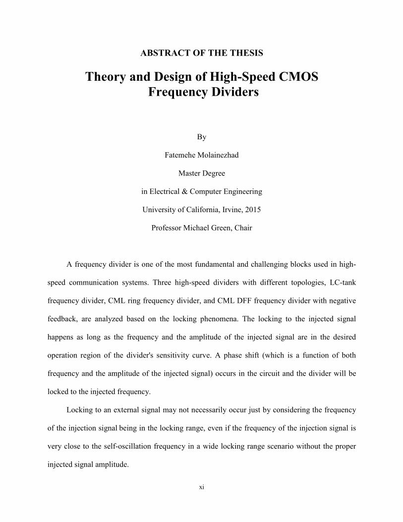
ABSTRACT OF THE THESIS
Theory and Design of High-Speed CMOS Frequency Dividers
By
Fatemehe Molainezhad
Master Degree
in Electrical & Computer Engineering
University of California, Irvine, 2015
Professor Michael Green, Chair
A frequency divider is one of the most fundamental and challenging blocks used in high-
speed communication systems. Three high-speed dividers with different topologies, LC-tank
frequency divider, CML ring frequency divider, and CML DFF frequency divider with negative
feedback, are analyzed based on the locking phenomena. The locking to the injected signal
happens as long as the frequency and the amplitude of the injected signal are in the desired
operation region of the divider's sensitivity curve. A phase shift (which is a function of both
frequency and the amplitude of the injected signal) occurs in the circuit and the divider will be
locked to the injected frequency.
Locking to an external signal may not necessarily occur just by considering the frequency
of the injection signal being in the locking range, even if the frequency of the injection signal is
very close to the self-oscillation frequency in a wide locking range scenario without the proper
injected signal amplitude.

xii
To measure the phase shift, ϕ (Ainj , ωinj) when the oscillator is locked to the injected
frequency, a novel procedure is developed. This procedure gives us a very precise tool to
measure the locking phase, instantaneous phase, or the phase between any two signals inside the
topology loop and provides a good ability for better understanding of the injection locking
concept and the behavior of the divider in the presence of an injected signal. The simulations are
using transistor models from TSMC 65nm CMOS process.

1
CHAPTER 1. INTRODUCTION
1.1 Overview
A frequency divider is a fundamental block in many systems. Such circuits are widely used
in high-speed communication systems and are considered as one of the most challenging blocks
to design in both wired and wireless transceivers [2]. Frequency dividers have been the subject of
extensive study for decades and a number of papers have been published about this subject.
Different approaches for injection locking phenomena have been investigated and several novel
frequency dividers that allow for higher frequencies and wider locking ranges have been
proposed.
In [4], it is described how the injection of an external signal into an oscillator affects both
the instantaneous amplitude and instantaneous frequency if the self-oscillation frequency is close
to the injection frequency. Using the assumption that the time constants in the oscillator circuit
are small compared to the length of one beat cycle, a differential equation is derived which gives
the phase between the oscillator output voltage and the injected signal as a function of time.
In [5], it is shown that locking to an external signal can occur when the frequency of the
injected signal is within a certain range of frequencies, called the "locking range," that contains
the self-oscillation frequency. An oscillator is said to be locked when the phase difference θ
between the locking signal and the oscillator is constant, so that the instantaneous frequency
difference, dθ /dt, is equal to zero.
In [6], it is presented if the amplitude and frequency of Iinj are chosen properly, the circuit
indeed oscillates at ωinj rather than at ωo and injection locking occurs.

2
In [1], two main categories of clock dividers are described: The first category includes
those that operate entirely based on injection locking, such as the LC-tank and the ring oscillator
frequency dividers. The second category includes divide-by-two circuits based on D flip-flops
(DFF) realized by current mode logic (CML) with negative feedback. In the latter category due
to the presence of nonlinearities, a wider frequency locking range, which is usually desirable, can
result.
In this thesis, three different topologies, LC-tank, CML ring, and CML DFF frequency
dividers are designed to achieve higher operation speed and minimum power consumption. They
are analyzed based on the following condition: As long as the frequency ωinj = ωo + ∆ω and the
amplitude Ainj of the injected signal are in the desired operation region of the frequency divider's
sensitivity curve, a phase shift, ϕ (Ainj , ωinj) will occur in the circuit and the oscillator will be
locked to the injected frequency.
The DFF frequency divider has a very wide sensitivity curve, which is a big advantage for
this topology. On the other hand, the frequency divider realized by a CML ring oscillator has a
higher self-oscillation frequency, but its sensitivity curve is not as wide as that of the DFF
frequency divider. Finally, an LC-tank frequency divider has a very narrow sensitivity curve, but
its self-oscillation frequency is much higher than either of the other two topologies and thus it is
suitable to be used in some applications for very high-frequency operation.
The variations of instantaneous frequency and phase are analyzed for all three dividers.
The instantaneous frequency can vary due to both changing the amplitude of the injection signal
and/or changing the phase between the injection and the oscillation signals. Controlling the
amplitude and the starting time to inject the signal can be used to reduce the settling time and
allow a faster locking to the injected frequency.

3
Based on the model of each topology and the concept of injection locking, the relationship
between the instantaneous and the locking phase is mathematically formulated. The analytical
results are then compared with the simulation results utilizing a procedure that is developed to
measure locking phase, instantaneous phase, or the phase between any two signals.
1.2 Outline
The remainder of thesis is organized as follows. Chapter 2 provides an overview of
published work on frequency dividers with an emphasis on high-speed clock dividers based on
the LC-tank frequency divider, CML ring frequency divider, and DFF frequency divider. This
overview covers the theoretical analysis of injection locking concept, frequency locking range,
and a derivation of the instantaneous phase, dθ /dt.
Chapter 3 analyzes the three divider topologies based on the injection-locking concept and
their sensitivity curves. The instantaneous frequency and phase when an external signal is
injected is analyzed in detail. A procedure is developed to measure the phase between two the
signals and verifying that the derivative of the instantaneous phase is equal to zero when the
divider locks to the injected frequency.
Chapter 4 models the three divider topologies, and equations are derived for the locking
phase and the instantaneous phase. The analytical results are discussed and compared with the
simulation results that are generated using transistors models from TSMC 65nm CMOS process.
Chapter 5 summarizes the findings and the conclusions.

4
CHAPTER 2. REVIEW OF PUBLISHED WORK
2.1 A Study of Injection-Locking and Pulling in Oscillators
A study of injection locking and pulling between coupled oscillators realized in CMOS
integrated circuits was reported in [6]. This paper describes the concept of injection locking,
based on Adler's formulation [6]. In the simple oscillator shown in Figure 2-1(a), the resonance
frequency of the tank is ωo = 1/ LLC . The ideal inverter provides the complementary 180o
phase shift which is needed to close the feedback loop and ensures the oscillation.
Figure 2-1 (a) Conceptual oscillator, (b) Frequency shift by injection, (c) Open-loop characteristics, and
(d) Phase difference between input and output currents [6].
Figure 2-1(b) shows that conceptual oscillator when an external signal is injected to the
output node. As described in [6], “if the amplitude and frequency of Iinj are chosen properly”,
injection locking occurs and the circuit oscillates at the injection frequency rather than at ωo. By

5
considering this condition the paper describes that the tank provides phase ϕo at ωinj ≠ωo,
therefore Vout rotates with respect to the sum current IT. It also describes that Iinj forms an angle
θ with Iosc such that the output voltage becomes aligned with resultant current. As a result, Vout
and Iinj must have a phase difference as shown in Figure 2-1(d). Using this concept of injection
locking, the locking range for LC-tank oscillator is formulated as following:
2
2
1
1..2
osc
injosc
injoinjo
III
IQ
−
=−ωωω (2-1)
The above equation shows how the amplitude of injected signal changes the locking range.
When the amplitudes of injected signal decreases while the injection frequency is held fixed, to
maintain phase ϕo which corresponds to the oscillation frequency, Iosc must form a bigger angle
with respect to Iinj. This paper also shows the application of the injection locking when oscillator
operates as a divide by two and investigates the nonlinearities in injection locking for LC-tank
oscillator.
2.2 Analysis of Nonlinearities in Injection-Locked Frequency Dividers
Analysis of nonlinearities in injection-locked frequency dividers is reported in [2]. This
paper investigated the locking range of frequency dividers and it was shown that the wider
locking range as the case for CML DFF frequency divider is due to the presence of
nonlinearities. The paper also presents a different approach to the analysis of nonlinearities in
ILFD and introduces a new definition and then proposes a new frequency divider topology based
on the new definition.

6
Figure 2-2 (a) Current injection mode of CML-DFF divider, (b) Schematic of new frequency divider [2].
Figure 2-2(a) shows an equivalent schematic of a conventional DFF divider, but with half-
rate current sources Iinj injected directly into the output nodes. As discussed in [2], it can be
shown that this is equivalent to the normal voltage injection with an appropriate conversion
factor, but lends itself better to a more detailed analysis. If the divider is under free-running
condition, then the drain currents Id are equivalent to Iosc. Itotal is the total current conducted
through the resistors. The phase relationships between currents Iinj, Iosc, and IT determine the
divider frequency range. For normal injection locking, as the case for LC or ring oscillator
dividers, it is generally assumed that all three currents stay in phase at the self-oscillation
frequency, regardless of the amplitude of the injected current. However as shown in [2], this does
not hold for the DFF clock divider.
A new definition is introduced in [2]: the In-Phase Frequency, which is the frequency at
which injected current signal, Iinj, Iosc, and IT, all remain in phase as a function of a given
amplitude of Iinj. The fundamental cause of the strong nonlinearity existing in the DFF frequency
divider can be narrowed down to the latch structure. Then the paper proposes a new frequency
divider topology based on that technique which provides robust operation and wide lock-in while
exhibiting higher operating frequency, as shown in Figure 2-2(b). The new topology employs a
cross-coupled source follower in place of the latch, which maintains nonlinearity similar to that

7
of the conventional DFF clock divider, while decreasing the capacitance at the output nodes,
thereby increasing the self-oscillation frequency.
2.3 A Study of Locking Phenomena in Oscillators
A study of locking phenomena in oscillators is reported in [4]. This paper explains how the
instantaneous amplitude and frequency of vacuum tube-based oscillators are both affected when
an external signal with a frequency very close to the natural frequency of the oscillator is injected
to the loop. A differential equation for the phase between feedback and injected signals as a
function of time is derived under the assumption that time constants in the oscillator are small
compared to the oscillation period.
The main purpose of this paper is to derive a differential equation for the oscillator phase
as a function of time and how it is related to the phase and amplitude relationships between
oscillator voltage and injected signal. The derived equation also describes the transient and
steady state behaviors of the oscillator. It is assumed in the analysis that the frequency of the
injected signal is close to the self-oscillation frequency.
Figure 2-3 (a) Adler's model for oscillator circuit, (b) Vector diagram of instantaneous voltages for
oscillator [4].

8
Adler investigated locking phenomena in vacuum tube-based oscillators using the model in
Figure 2-3(a). The grid voltage, Eg is the vector sum of the injected voltage EL and the tank
voltage EF which is transformer-coupled into the grid and denoted as Eo in the diagram. The
following symbols are used:
ωo = self-oscillation or “natural” frequency
ωl = frequency of injected signal
∆ωo= “undisturbed” beat frequency (or inherent frequency difference )(ωo -ωl )
ω = oscillator's instantaneous frequency
∆ω = instantaneous beat frequency (or instantaneous frequency difference )(ω -ωl)
Q = quality factor of tuned circuit.
Using the following three assumptions, the differential equation for the model in Figure
2-3(a) was developed.
1) ωo /2Q>>∆ωo; that is, the locking frequency should be very close to the natural frequency
of the tuned circuit.
2) T <<1/∆ωo; that is, the time contestants in the oscillator are small compared to the
oscillation period.
3) EL / Eo <<1; that is, the amplitude of injected signal is much smaller than the output
voltage.
Adler's derivation of the phase as a function of time was based on the vector diagram of
instantaneous voltages shown in Figure 2-3(b). Under the presence of an injected signal, there is a
phase angle ϕ between the voltage E returned through the feedback circuit and the grid voltage
Eg. Assuming EL / Eo <<1, Figure 2-3(b) gives:

9
ααϕ sin)sin(EE
EE L
o
L −=−
= (2-2)
It is also concluded in [4] that under the presence of an injected signal, the instantaneous
frequency would exceed ωo by an amount which will produce a lag equal to ϕ. For locking
frequencies close to the oscillator's natural frequency, this phase can be written as:
][)]()[()( 0 olol dtdAAA ωαωωωωωωϕ ∆−=−−−=−= (2-3)
where A=2Q/ωo for small values of ϕ.
Combining equations (2-1) and (2-2) would result Adler's equation [4]:
ool
QEE
dtd ωαωα
∆+−= sin2
. (2-4)
Equation (2-3) derives the instantaneous angular beat frequency, ∆ω= dα/dt as a function
of the oscillator's natural frequency, oscillator voltage and injected signal amplitudes, and the
phase relationship between them.

10
CHAPTER 3. High Frequency Clock Dividers
A frequency divider is a challenging block, especially for high-frequency and low-power
operation used in high-speed communication systems. In this chapter, three different topologies,
LC-tank, CML ring, and CML DFF frequency dividers are analyzed based on the following
locking condition: As long as the frequency, ωinj = ωo + ∆ω and the amplitude, Ainj of the
injected signal are in the desired operation region of the frequency divider's sensitivity curve, a
phase shift,ϕ (Ainj , ωinj) will be created and the oscillator is locked to the injected frequency.
The instantaneous frequency and phase of the frequency dividers are analyzed when the
divider is under an injected signal. A new procedure is developed to measure any phase
difference between two signals when the oscillator is locked. The simulations are using transistor
models from TSMC 65nm CMOS process with the power supply voltage of 1.2V.
In the following sections, the three types of frequency dividers are discussed in detail.
3.1 High-Speed Frequency Divider Based on CML D Flip-Flop
Since the CML DFF frequency divider is primarily based on a CML structure, one of the
key points to analyze this topology is the design and specifications of CML buffer.
3.1.1 CML Buffer
Figure 3-1 shows the structure and the dc characteristics of a simple resistive load CML
buffer. In such structures, the large-signal characteristic of the transistors is of primary
importance. In other words, the intention is to have the current steered completely from one leg
to another at the target speed.

11
Figure 3-1 (a) CML differential pair [10], (b) Characteristics of a simple CML buffer [9].
To derive the voltage swing that is illustrated in Figure 3-1, the exact values of high and
low output voltages should be determined. When the input voltage, Vin+ goes high, the tail
current Iss is conducted through transistor M1 and as a result Vout- falls to Vdd - IssR. Similarly Vout+
reaches Vdd. These voltages correspond to output low and output high, respectively. The dc
characteristics of a simple resistive load CML buffer is shown in Figure 3-1(b). Since output
voltages high and low are VHigh=Vdd and VLow=Vdd - IssR respectively, the output swing voltage is,
Vswing= VHigh - VLow= IssR [10]. The condition to achieve full current switching is given by:
min2)( V
LWC
IVVVoxn
ssIssIdtGSswing ==−≥ =
µ (3-1)
where Vmin is the minimum differential voltage that is required to completely turn off one
transistor. By dividing both sides of (3-1) by Vmin, we have (Vswing / Vmin) >1 as the condition for
current being fully switched [10].
Typical chosen Vswing is equal to 0.3×Vdd to guarantee, 1) being large enough to allow
sufficient gain-bandwidth product and 2) being small enough to prevent transistors from going
into triode [10].
One systematic approach to size and bias CML structures for high-speed operations is to
cascade three stages of similar buffers and connect an ideal signal source of the desired speed to

12
the input of the first buffer. This configuration represents a close to real condition for the middle
buffer since its input signal is generated from a buffer with real load and its output stage is
looking at a real load. The buffer size, both transistors and resistors, and bias condition should be
made in such a way that when looked differentially, the input and the output of the second buffer
have the same voltage swing. This ensures that 1) the input voltage swing is large enough to steer
the current completely from one leg to another and also 2) provides similar voltage swing for the
next stage. Having similar voltage swings at both input and output of middle buffer guarantees
that signal logic will be passed through stages at the desired speed.
To determine low power consumption, considering the electro-migration constraints for the
buffer, the proper value for current source, Iss is chosen to be 400uA [10]. Assuming Vdd =1.2V,
the typical swing voltage is equal to Vswing = 0.3×Vdd = 0.4V. On the other hand, Vswing= IssR, as a
result the load resistance should be R=1k. Based on these values the proper W/L ratio of the
transistors would be 60 which is resulted from simulation.
3.1.2 CML D Flip-Flop Divider
A simple topology of a divide-by-two D-flip-flop frequency divider, shown in Figure 3-2,
consists of two cascaded D-latches with a negative feedback configuration.
Figure 3-2 Topology of a DFF frequency divider.

13
A static DFF frequency divider, realized by current mode logic, (CML) with negative
feedback is shown in Figure 3-3. The maximum operation frequency of this structure is generally
limited by its parasitic capacitances.
Figure 3-3 CML D Flip-Flop clock divider schematic.
Depending on the design specification, each CML D-latch can utilize different components
and structures as output load. Initially, the static loads are implemented by fixed resistors. This
implementation suffers from the process variations. However, it has the advantage of providing
the same rising and falling times that are equal to τ=R×CL. The load capacitance CL is the sum of
the buffer's gate-source parasitic capacitance Cgs,b2 of the second latch, the gate-source parasitic
capacitance Cgs,c1 of cross-coupled transistor for the first latch, the buffer's drain-substrate
parasitic capacitance Cds,b1 for the first latch, and the drain-substrate parasitic capacitance Cds,c1
of the cross-coupled for the first latch where Cgs = γCoxWL [10].
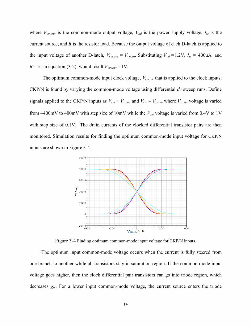
The common-mode output voltage for the circuit shown in Figure 3-3, is given by:
RIVV ssddoutcm ×−= 5.0, (3-2)
14
where Vcm,out is the common-mode output voltage, Vdd is the power supply voltage, Iss is the
current source, and R is the resistor load. Because the output voltage of each D-latch is applied to
the input voltage of another D-latch, Vcm,out = Vcm,in. Substituting Vdd =1.2V, Iss = 400uA, and
R=1k in equation (3-2), would result Vcm,out =1V.
The optimum common-mode input clock voltage, Vcm,clk that is applied to the clock inputs,
CKP/N is found by varying the common-mode voltage using differential dc sweep runs. Define
signals applied to the CKP/N inputs as Vcm + Vramp and Vcm − Vramp where Vramp voltage is varied
from −400mV to 400mV with step size of 10mV while the Vcm voltage is varied from 0.4V to 1V
with step size of 0.1V. The drain currents of the clocked differential transistor pairs are then
monitored. Simulation results for finding the optimum common-mode input voltage for CKP/N
inputs are shown in Figure 3-4.
Figure 3-4 Finding optimum common-mode input voltage for CKP/N inputs.
The optimum input common-mode voltage occurs when the current is fully steered from
one branch to another while all transistors stay in saturation region. If the common-mode input
voltage goes higher, then the clock differential pair transistors can go into triode region, which
decreases gm. For a lower input common-mode voltage, the current source enters the triode

15
region. Based on the simulation result shown in Figure 3-4 and the common-mode output voltage
value, Vcm,out =1, and the optimal value for clkcmV , would be 0.6 volt subsequently.
The circuit parameters of the DFF frequency divider shown in Figure 3-3 are listed in
Table 3-1.
Table 3-1 Circuit parameters of the DFF frequency divider.
3.1.3 Plotting Sensitivity Curve
A clock divider can be accurately characterized by its sensitivity curve [3], which specifies
the minimum injected input clock amplitude, at a given frequency, for the divider to lock.
The procedure that is used to plot the frequency divider's sensitivity curve is defined by
following steps:
1) Find the self-oscillation frequency (Fself) when the clock amplitude is zero as shown in
Figure 3-5(a).
2) Apply a differential sinusoid voltage to the differential CKP/N inputs with maximum
clock amplitude (Vm) which is Vswing /2. Run a parametric analysis sweeping the clock
frequency, for example from ωo -10G to ωo +10GHz. Monitor the frequency of
differential output voltage using Cadence's "frequency" function. If the range is too wide
or too narrow change it until to find the minimum (FMin-m) and maximum (FMax-m)
frequencies that oscillator operates as the divide-by-two correctly as is shown in Figure
3-5(b).
Circuit Parameters Iss Vdd W/L R
Value 400u 1.2v 60 0.9k
16
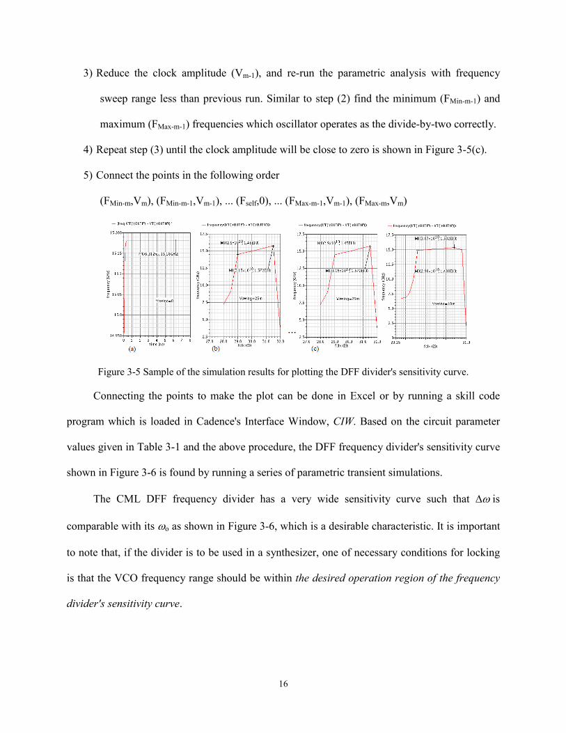
3) Reduce the clock amplitude (Vm-1), and re-run the parametric analysis with frequency
sweep range less than previous run. Similar to step (2) find the minimum (FMin-m-1) and
maximum (FMax-m-1) frequencies which oscillator operates as the divide-by-two correctly.
4) Repeat step (3) until the clock amplitude will be close to zero is shown in Figure 3-5(c).
5) Connect the points in the following order
(FMin-m,Vm), (FMin-m-1,Vm-1), ... (Fself,0), ... (FMax-m-1,Vm-1), (FMax-m,Vm)
Figure 3-5 Sample of the simulation results for plotting the DFF divider's sensitivity curve.
Connecting the points to make the plot can be done in Excel or by running a skill code
program which is loaded in Cadence's Interface Window, CIW. Based on the circuit parameter
values given in Table 3-1 and the above procedure, the DFF frequency divider's sensitivity curve
shown in Figure 3-6 is found by running a series of parametric transient simulations.
The CML DFF frequency divider has a very wide sensitivity curve such that ∆ω is
comparable with its ωo as shown in Figure 3-6, which is a desirable characteristic. It is important
to note that, if the divider is to be used in a synthesizer, one of necessary conditions for locking
is that the VCO frequency range should be within the desired operation region of the frequency
divider's sensitivity curve.

17
Figure 3-6 Sensitivity curve for the DFF frequency divider.
3.1.4 Procedure to Measure Phase Difference Between Two Signals
To measure the phase shift, ϕ when the oscillator is locked to the injected frequency a
novel procedure is developed. This procedure gives us a very precise tool to measure the locking
phase, instantaneous phase, or any phase shift between two signals inside the topology loop and
provides a good ability for better understanding of injection locking concept and the behavior of
the divider under an impressed signal. The procedure that is used to measure the phase difference
between two signals is defined by following steps:
1) Run the transient simulations with the desired setup.
2) Find the time of zero crossing points for the rising edge of any two desired signals
(voltage or current), Sig1t0, Sig1t1, ... Sig1tn and Sig2t0, Sig2t1, ... Sig2tn
where Sig1tm is the time of the mth zero crossing point of the first signal, Sig1.
3) For all the zero crossing times (t0, t1, ... tn), calculate the following:
a. Freqm = 1/(Sig1tm−Sig1tm-1) for m=0 ... n

18
where Freqm is the inverse of the time difference between two consecutive zero
crossing points.
b. Phasem = 360 × (Sig2tm−Sig1tm) × Freqm for m=0 ... n
where Phasem is the mth phase shift between the two signals
Implementation of the procedure is done by a skill code program which is loaded in
Cadence's Interface Window, CIW or in the ocean program.
3.1.5 Analyzing Instantaneous Frequency and Phase for DFF Divider
In this section, the variation of instantaneous frequency is analyzed. The instantaneous
frequency can vary due to 1) changing the amplitude of the injection signal and/or 2) changing
the phase between the injection signal and the oscillation output signal. When an external signal
is injected to the loop of the oscillator, there is a transient duration that the amplitude and the
instantaneous frequency (the difference between two consecutive zero crossing points) of the
oscillation changes until the divider locks and they are settled. Note that the frequency and the
amplitude of the injected signal should be in the desired operation region of the frequency
divider's sensitivity curve in order to guarantee the locking happens.
To investigate the variation of instantaneous frequency, a differential sinusoid voltage
signals is applied to the differential CKP/N inputs of the DFF frequency divider shown in Figure
3-3 when the DFF frequency divider is free running. Figure 3-7 shows an example of the
injected signal and the resulting divider output signal.

19
Figure 3-7 Simulation results for an injected signal and its effect on instantaneous frequency.
Figure 3-7(a) shows two signals: 1) the differential clock input with amplitude equal to
400mV and injection frequency equal to 32GHz which is applied at the starting time of 4ns and
2) the differential output of the DFF frequency divider which oscillates at free running frequency
of 15.18GHz until 4ns and then locks after a few cycles to the 16GHz frequency that is half of
the input 32GHz injection frequency. Figure 3-7(b) shows the locking states and also the
transition of oscillation frequency between the two stable conditions. Figure 3-7(c) shows the
phase between the output and injection currents. The derivative of the phase is zero when the
divider locks to the frequency of the injected signal as shown in Figure 3-7(d).
To determine the variation of instantaneous frequency when the amplitude of the injection
signal is changed, the following tests are done. Figure 3-8 shows the results.

20
Figure 3-8 Simulation results when the clock amplitude is changed for DFF divider.
Figure 3-8(a) shows just a small change in the instantaneous frequency when the 34GHz
clock amplitude is varied from 200mV to 400mV with the step size of 100mV. For clock
amplitudes less than 50mV, the divider cannot lock to the 34GHz input frequency. Figure 3-8(b)
shows the result when a 30.4GHz input clock amplitude is varied from 20mV to 50mV with the
step size of 10mV. Simulation results show that amplitude variations of injection signal do not
have notable impact on the instantaneous frequency. Figure 3-8(c) shows the derivative of the
phase for a few cases when the divider locks to the frequency of the injected signal.
We now consider the effect of the time at which the injection signal is applied while the
clock amplitude and frequency are held constant.
The starting time when the clock is injected to the divider, can occur anytime during the
oscillation cycle. For example, it can occur around the zero crossing in rising or falling edges or
in the peaks of the cycle.

21
Figure 3-9 Simulation results when the clock is applied at different starting times for DFF divider.
Figure 3-9 shows the simulation result when the clock is applied to the divider at different
stating times. Figure 3-9(a) shows the case when starting time is at 3.942ns and is around the
zero crossing in the rising edge of oscillation cycle. Figure 3-9(b) shows the case when starting
time is at 3.958ns and is around the peak of the oscillation cycle. Figure 3-9(c) shows the case

22
when starting time is at 3.978ns and is around the zero crossing in the falling edge of oscillation
cycle. As the simulation results show, the instantaneous frequency is changed significantly by
changing the phase between the injection signal and the oscillation signal. The transient response
behavior and the settling time are both affected by the variation of the phase between the
injection signal and the oscillation signal. However, in all cases the same steady-state behavior is
reached.
More simulations are done to show how the settling time is affected by the variation of the
phase between the injection and the oscillation signals. In the following tests the starting time to
inject the clock is changed by constant step size during one period of the divider oscillation.
Figure 3-10 shows the simulation results.
Figure 3-10 Transient response due to phase variations of the injection signal for DFF divider.
Figure 3-10(a) shows the results when the starting time to inject the clock is changing from
3.997ns to 4.007ns with the step size of 1ps. The clock amplitude is 300mV and its frequency is
constant and equal to 30.4GHz. Figure 3-10(b) shows the simulation results when the clock
amplitude is reduced to 30mV.
Simulation results show that the settling time is affected significantly by the variation of
the phase between the injection and the oscillation signals and the injection signal amplitude. By

23
controlling the clock amplitude and the starting time to inject the clock, the settling time can be
reduced and as a result a faster locking to the injected frequency occurs.
3.2 High-Speed Frequency Dividers Based on CML Ring
The problem with a CML divide-by-two D-flip-flop frequency divider is that the output
nodes of two D-latches see a large capacitance load. The cross-coupled transistor pair used in the
D-latch is one of the main contributors to the output capacitance [3]. Different techniques and
topologies are suggested to reduce [1], [7] or eliminate [3] the parasitic capacitance of the cross-
coupled transistor pair. One of the topologies that eliminates the cross-coupled transistor pairs, is
the CML ring frequency divider which is realized by CML buffers as shown in Figure 3-11.
Figure 3-11 CML ring clock divider schematic.
By eliminating the cross-coupled transistor pair as shown in Figure 3-11, the capacitance at
output nodes is reduced and as a result the higher speed can be achieved [3]. However, it has the
same rising and falling times that are equal to τ=RCL which CL is defined by CL = Cds,bi
+Cgs,b(i+1). The capacitance, Cds,bi is the buffer's drain-substrate parasitic of any given buffer and
capacitance Cgs,b(i+1) is the buffer's drain-substrate parasitic of the following buffer, where Cgs =

24
γCoxWL [10]. As a result the load capacitance size, CL of the CML ring frequency divider is the
half of the load capacitance size of the CML DFF frequency divider.
The CML ring frequency divider exhibits a substantial increase in the maximum frequency
with the wide range of operation. In this configuration CML buffers function as both low-pass
filter and amplifier., Also the CML buffer functions as a single balanced mixer when a full rate
clock is applied. A realization of single balanced mixer is shown in Figure 3-12.
Figure 3-12 Realization of single balanced mixer.
It is assumed all the transistors are in saturation region and identical. When a sinusoidal
clock signal, VCK is applied to the CLK input, the drain current of the transistor M1, will be
Id1=(gmVCK +Iss). The clock signal is defined as VCK =Acosωt. A differential sinusoid voltage is
applied to the differential VinP/N inputs and the positive input is VinP =Bcosωot. This is a time
variant linear system, therefore I = Id1 × Iin, where Iin is gmVinP/N, subsequently:
NinPmCKmss VgVgII /)( ×+= (3-3)
By substituting VCK =Acosωt and VinP/N =Bcosωot in (3-3), the result would be:
tBgtAgII ommss ωω cos)cos( ×+=
ttABgtBgII omomss ωωω coscoscos 2+= (3-4)
We know that cosωot×cosωt=1/2(cos(ω -ωo)t + cos(ω +ωo)t), and cos(ω +ωo)t is filtered
out by its RC low pass filter. Therefore (3-4) can be simplified to:

25
tABgtBgII omomss )cos(21cos 2 ωωω −+= (3-5)
When the divider is locked, ω is equal to 2×ωo , (3-5) can be written as:
I = K cosωot (3-6)
where K = Iss gmB +0.5AB(gm)2.
3.2.1 Circuit Parameters Design
The CML buffer presented in Section 3.1.1 is used in the ring oscillator design. When Iss is
set to 600uA and Vswing is set to 0.4V, R=0.9k. The transistor size of the ring buffers have the
same ratio W/L of 60 as the previously designed CML buffer's transistor size.
The common-mode output voltage, Vcm,out for the circuit that is shown in Figure 3-11, is
Vcm,out = Vdd − 0.5× IssR. Because the output voltage of each buffer is applied to the input voltage
of next buffer, we have Vcm,out = Vcm,in , where Vcm,in is the common-mode input voltage for each
buffer. By knowing Vdd =1.2V, Iss = 600uA, and R=0.9k, we have Vcm,out = Vcm,in =0.93V.
The optimum common-mode input clock voltage, Vcm,clk that is applied to the clock inputs,
CKP/N inputs is the same as DFF frequency divider's common-mode input clock voltage. The
optimal value for clkcmV , is 0.6V. The circuit parameters of the ring frequency divider shown in
Figure 3-11 are listed in Table 3-2.
Table 3-2 Circuit parameters of the ring frequency divider.
Circuit Parameters Iss Vdd W/L R
Value 600uA 1.2V 60 0.9k

26
3.2.2 CML Ring Frequency Divider's Sensitivity Curve
The procedure that is defined in Section 3.1.3 is used to plot the sensitivity curve of the
ring frequency divider shown in Figure 3-11. Based on the circuit parameter values in Table 3-2
and the defined procedure, the points are obtained to plot the sensitivity curve. In the first step,
the self-oscillation frequency is found. Figure 3-13 shows the self-oscillation frequency of the
ring frequency divider.
Figure 3-13 Self oscillation frequency for ring divider.
Figure 3-13 gives the (Fself,0) point in the sensitivity curve, where Fself=27.16GHz is the
self-oscillation frequency when clock amplitude is zero volts. In next steps all the points (FMin-
m,Vm) and (FMax-m,Vm), the minimum and maximum output frequencies when clock amplitude is
defined at certain value in the sensitivity curve are found. For example when the clock amplitude
is 400mV, the simulation gives two points as shown in Figure 3-14.

27
Figure 3-14 An example of finding two points in the sensitivity curve for Vm=400mV.
Figure 3-14 provides the (21GHz, 400mV) and (31.5GHz, 400mV) points in the sensitivity
which are the minimum and maximum output frequencies that divider locks when clock
amplitude is 400mV. When clock amplitude is varied, the minimum and maximum output
frequencies that divider locks will be changed. Therefore, similar to this example all the points
are found and connected to plot the ring frequency divider's sensitivity curve shown in Figure
3-15.
Figure 3-15 Sensitivity curve for 4-stage ring frequency divider.
In summary CML ring frequency divider has a wide sensitivity curve, but is not as wide as
CML DFF frequency divider sensitivity curve and its self-oscillation frequency is also higher.

28
3.2.3 Analyzing Instantaneous Frequency and Phase Shift
The variation of instantaneous frequency is analyzed similar to CML DFF frequency
divider. As described in Section 3.1.5, the instantaneous frequency can vary due to 1) changing
the amplitude of the injection signal and/or 2) changing the phase between the injection signal
and the oscillation output signal by applying the injection signal at different starting time during
the oscillation cycle. To investigate the variation of instantaneous frequency, a differential
sinusoidal voltage signal is applied to the differential CKP/N inputs of the CML ring frequency
divider shown in Figure 3-11 when the ring frequency divider oscillates in its free running
frequency. It should be noted that the frequency and the amplitude of the injected signal should
be in the desired operation region of the divider's sensitivity curve in order to guarantee that
locking occurs. Figure 3-16 shows an example of the injected signal and the resulting divider
output signal.
Figure 3-16 An example of the effect of an injected signal on instantaneous
frequency and phase for ring divider.
29
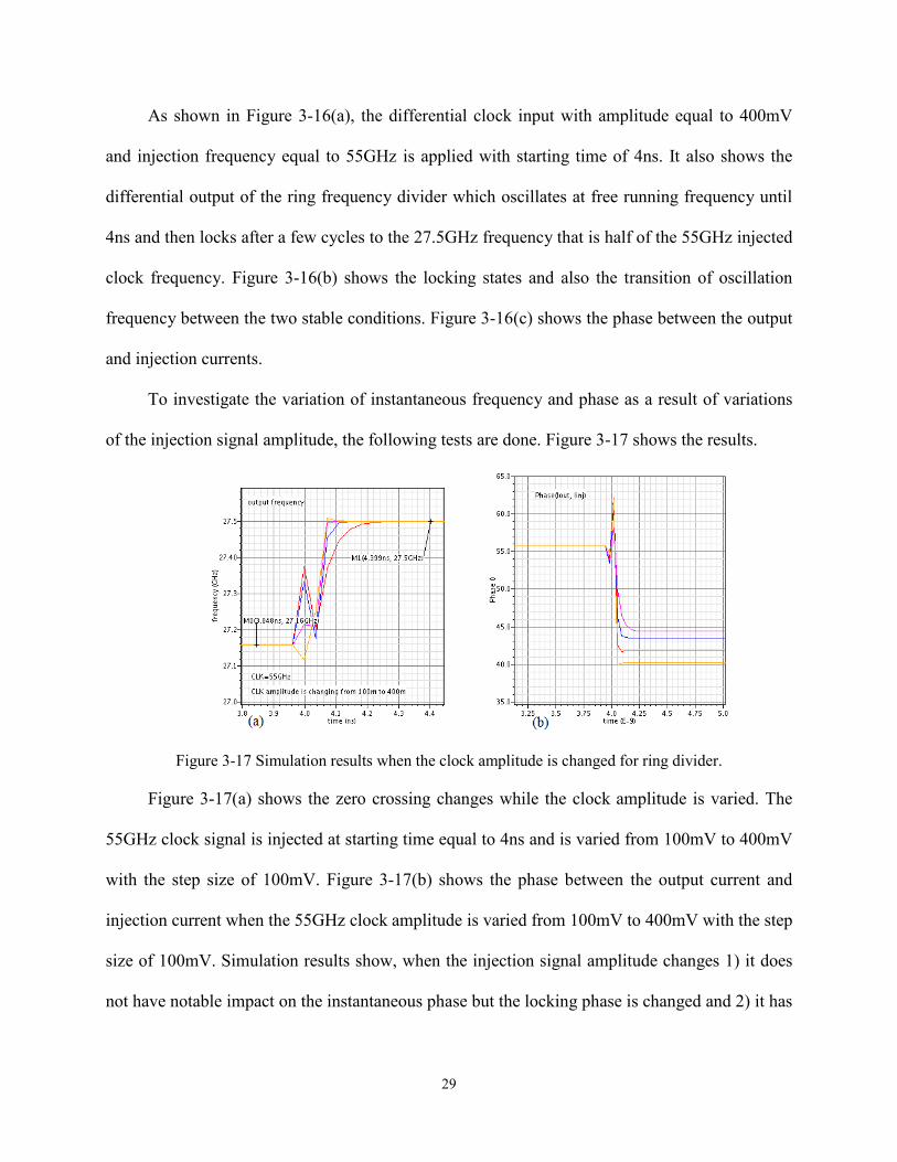
As shown in Figure 3-16(a), the differential clock input with amplitude equal to 400mV
and injection frequency equal to 55GHz is applied with starting time of 4ns. It also shows the
differential output of the ring frequency divider which oscillates at free running frequency until
4ns and then locks after a few cycles to the 27.5GHz frequency that is half of the 55GHz injected
clock frequency. Figure 3-16(b) shows the locking states and also the transition of oscillation
frequency between the two stable conditions. Figure 3-16(c) shows the phase between the output
and injection currents.
To investigate the variation of instantaneous frequency and phase as a result of variations
of the injection signal amplitude, the following tests are done. Figure 3-17 shows the results.
Figure 3-17 Simulation results when the clock amplitude is changed for ring divider.
Figure 3-17(a) shows the zero crossing changes while the clock amplitude is varied. The
55GHz clock signal is injected at starting time equal to 4ns and is varied from 100mV to 400mV
with the step size of 100mV. Figure 3-17(b) shows the phase between the output current and
injection current when the 55GHz clock amplitude is varied from 100mV to 400mV with the step
size of 100mV. Simulation results show, when the injection signal amplitude changes 1) it does
not have notable impact on the instantaneous phase but the locking phase is changed and 2) it has

30
a notable impact on the instantaneous frequency and the settling time. The settling time increases
when the injection signal amplitude decreases.
Now, the clock amplitude and frequency are held constant while the starting time to inject
the clock is changed. The following tests show the effect of the different starting time to apply
the clock on the instantaneous frequency. The starting time can occur at anytime during the
oscillation cycle. Figure 3-18 shows an example of the injected signal and the resulting divider
output signal, while the starting time to inject the clock is changed.
Figure 3-18 Simulation results when the clock is applied at different starting times for ring divider.
Figure 3-18(a) shows the result when the starting time to inject the55GHz, 400mV clock is
changing from 3.999ns to 4.035ns with a step size of 4ps. Figure 3-18(b) shows the phase
between the output current and injection current when the starting time to inject the clock is
varied from 3.999ns to 4.035ns with the step size of 4ps. Simulation results show when the
starting time to inject the clock is changing while the clock signal amplitude and clock frequency
are constant: 1) it has a notable impact on the instantaneous phase but the locking phase is not
changed and 2) it has a significant impact on the instantaneous frequency and the settling time.

31
The settling time decreases when the starting time of the injection signal is around the zero
crossing of oscillation cycle.
The time derivative of the phase difference between Iout and Iinj becomes zero and when the
frequency divider locks. Figure 3-19(a) shows this behavior during the self-oscillation and when
it locks to injected signal's frequency.
Figure 3-19 The instantaneous phase due to injection signal for ring divider.
3.3 High-Speed Frequency Dividers Based on LC-tank Oscillator
The LC-tank oscillator can be designed as either single-ended or differential type. The
differential type has higher rejection of common mode interferers and stronger attenuation of
even-order harmonics than the single-ended type. Therefore, the differential type is commonly
required in most applications although it needs more components and consumes more power.
The LC-tank frequency divider is realized by a differential LC-tank oscillator where input clock
is fed through the source as shown in Figure 3-20.

32
Figure 3-20 LC-tank frequency divider schematic.
The resonant frequency of the tank is ωo = 1/ LLC . This type of divider is suitable for
very high-frequency operation, however, it occupies a large area due to the on-chip inductor.
To design of the LC-tank oscillator parameters circuit, we use the same transistor size that
is used in the DFF and ring frequency dividers. The current source, Iss was set to 400uA. As
shown in Figure 3-20, the divider output is connected to the input of a CML buffer to provide a
realistic load capacitance. The capacitance CL is the sum of the gate-source parasitic capacitance,
Cgs,b of the buffer, the gate-source parasitic capacitance Cgs,c of the cross-coupled transistor pair,
the drain-substrate parasitic capacitance Cds,c of the cross-coupled transistor pair, the tank
capacitor, C, and parasitic capacitance of the inductor CP,L where Cgs = γCoxWL [10] and
CP,L=1/(Lω2SRF). For this circuit the self-resonant frequency of the inductor is 5 times the self-
oscillation frequency. Based on simulation results, the proper value for inductor is 1nH. The
circuit parameters of the LC-tank frequency divider shown in Figure 3-20 are listed in Table 3-3.
Table 3-3 Circuit parameters of the LC-tank frequency divider.
Circuit Parameters Iss Vdd W/L L C CL
Value 400uA 1.2V 60 1nH 3.69fF 13.16fF
33
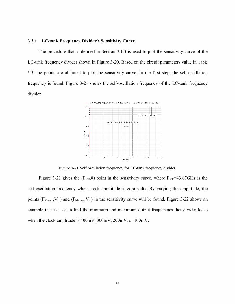
3.3.1 LC-tank Frequency Divider's Sensitivity Curve
The procedure that is defined in Section 3.1.3 is used to plot the sensitivity curve of the
LC-tank frequency divider shown in Figure 3-20. Based on the circuit parameters value in Table
3-3, the points are obtained to plot the sensitivity curve. In the first step, the self-oscillation
frequency is found. Figure 3-21 shows the self-oscillation frequency of the LC-tank frequency
divider.
Figure 3-21 Self oscillation frequency for LC-tank frequency divider.
Figure 3-21 gives the (Fself,0) point in the sensitivity curve, where Fself=43.87GHz is the
self-oscillation frequency when clock amplitude is zero volts. By varying the amplitude, the
points (FMin-m,Vm) and (FMax-m,Vm) in the sensitivity curve will be found. Figure 3-22 shows an
example that is used to find the minimum and maximum output frequencies that divider locks
when the clock amplitude is 400mV, 300mV, 200mV, or 100mV.

34
Figure 3-22 An example to find (FMin-m,Vm) and (FMax-m,Vm) points for the LC-tank divider.
Figure 3-22 gives (43.6GHz, 400mV) and (44.07GHz, 400mV) points for the minimum
and the maximum output frequencies that divider locks when clock amplitude is 400mV. For
clock amplitude of 300mV, (43.7GHz, 300mV) and (44.04GHz, 300mV) points are found. For
clock amplitude of 200mV, (43.76GHz, 200mV) and (43.98GHz, 200mV) points and for 100mV
(43.82GHz, 100mV) and (43.94GHz, 200mV) points are found respectively. Similar to this
example more points are found and connected to plot the LC-tank frequency divider's sensitivity
curve as shown in Figure 3-23.
Figure 3-23 Sensitivity curve for LC-tank frequency divider.

35
The LC-tank frequency divider has a very narrow sensitivity curve, but its self-oscillation
frequency is much higher than the other two topologies. This frequency divider is capable to
have a much higher self-oscillation frequency, therefore suitable to be used in some applications
for very high frequency operation.
3.3.2 Analyzing Instantaneous Frequency and Phase Shift for LC-tank
The variation of instantaneous frequency for the LC-tank is analyzed similar to the other
two frequency dividers. As described in Section 3.1.5, the instantaneous frequency can vary due
to 1) changing the amplitude of the injection signal and/or 2) changing the phase between the
injection signal and the oscillation signal by applying the injection signal at different starting
time during the oscillation cycle.
Figure 3-24 An injected signal and its effect on LC-tank frequency divider's output.
To investigate the variation of instantaneous frequency, a sinusoidal voltage signal is
applied to the clock input, CLK of the LC-tank frequency divider shown in Figure 3-20 when the
LC-tank frequency divider oscillates in its free running frequency. It should be noted that the

36
frequency and the amplitude of the injected signal should be in the desired operation region of
the LC-tank frequency divider's sensitivity curve in order to guarantee that locking happens.
Figure 3-24 shows an example of the injected signal and the resulting divider oscillation
output signal. As shown in Figure 3-24(a), the clock input with amplitude equal to 400mV and
injection frequency equal to 87.9GHz is applied with starting time at 4ns. It also shows the
differential output of the LC-tank frequency divider which oscillates at free running frequency
until 4ns and then locks after a few cycles to the 43.95GHz frequency that is half of the 87.9GHz
injected frequency. Figure 3-24(b) shows the locking states and also the transition of oscillation
frequency between the two stable conditions. Figure 3-24(c) shows the phase difference between
the output and injection signal and also shows the time derivative of the phase that is equal to
zero when the divider locks.
To determine the variation of instantaneous frequency as a result of changing the
amplitude of the injection signal while the injected frequency and the starting time to inject the
clock are held constant, the following tests are done. Figure 3-25 shows the results.
Figure 3-25 Simulation results when the clock amplitude is changed for LC-tank divider.

37
Figure 3-25(a) shows that the transition response changes while the 87.9GHz clock
amplitude that is injected at starting time equal to 4ns, is varied from 200mV to 400mV with a
step size of 100mV. Figure 3-25(b) shows the variations of phase when the 87.9GHz clock
amplitude is varied from 200mV to 400mV with the step size of 100mV. Simulation results
show, when the injection signal amplitude changes, it has a notable impact on the instantaneous
frequency and the settling time. The settling time increases when the injection signal amplitude
decreases. They also show that the locking phase between the output and injection signal is
changing when the clock amplitude is varied.
Now, the clock amplitude and frequency are held constant while the starting time to inject
the clock is changed. The following tests show the effect of the different starting time to apply
the clock on the instantaneous frequency. The starting time can occur at any time during the
oscillation cycle. Figure 3-26 shows an example of the injected signal and the resulting divider's
oscillation output signal, while the starting time to inject the clock is changed.
Figure 3-26 Simulation results when the clock is applied at different starting times for LC-tank divider.

38
Figure 3-26(a) shows the clock when the injection starting time is changing from 4.007ns
to 4.026ns with a step size of 3ps. The 87.9GHz clock amplitude is set to 100mV. Figure 3-26(b)
shows the transient response behavior of oscillation frequency between the two stable conditions
when the starting time to inject the signal is changing. Figure 3-26(c) and Figure 3-26(d) show
the variations of instantaneous phase when the injection starting time is changing from 4.007ns
to 4.026ns with a step size of 3ps. The simulation results show that the instantaneous frequency,
settling time and instantaneous phase are changed significantly by the variation of the phase
between the injection signal and the oscillation output signal. And also show that the locking
phase between the output and injection signal is constant when the starting time to inject the
signal is varied.
Figure 3-27 shows an example of the variation of instantaneous output frequency as a
result of changing the amplitude of the injection signal and the starting time to inject the clock
while the injected frequency is constant.
Figure 3-27 Simulation results when the clock amplitude and injection starting times are varied.
Figure 3-27 shows the changes in the transition response while the 87.9GHz clock
amplitude is varied from 400mV to 200mV with a step size of 100mV and also the starting time
to inject the clock is changing from 4.01ns to 4.024ns with a step size of 6ps. The simulation

39
results show that the instantaneous frequency and settling time are changed significantly and the
locking phase between the output and injection signal is changed when the clock amplitude is
varied.

40
CHAPTER 4. Analyzing Locking Phase
In this section, three different topologies, LC-tank frequency divider, CML ring frequency
divider, and CML DFF frequency divider, will be modeled. Based on model and topology, the
locking and the instantaneous phase equations will be derived. The analytical results will be
compared and discussed with the simulation results.
4.1 LC-Tank Frequency Dividers
For simplicity of the analysis, a differential half rate frequency current is injected into the
tank nodes instead of the clock voltage with full rate frequency as shown in Figure 4-1.
Figure 4-1 Schematic of the LC-tank frequency divider with current injected to the tank nodes.
This circuit shown in Figure 4-1 can be modeled as shown in Figure 4-2.

41
Figure 4-2 (a) Equivalent circuit, (b) Block diagram and (c) Vector representation of LC-tank divider.
An equivalent circuit for the LC-tank divider is shown in Figure 4-2(a), where iinj is the
injected current, id is the feedback current, and their sum is output current, io = id + iinj. The
block diagram equivalent is shown in Figure 4-2(b). A vector representation of the three currents
is shown in Figure 4-2(c) where the locking phase, ϕ is the angle between the feedback current id
and the sum current io, which goes to the load; phase θ is the angle between the feedback current
id and the current iinj that is injected into the drain.
Using the procedure to measure phases described in Section 3.1.1, Figure 4-3 is the
simulated vector representation of the three currents in Figure 4-2(c).
Figure 4-3 An example of simulation results showing vector representation of the three.

42
From Figure 4-2(c), we can write the sum current io as a complex number by the following
relation:
θθ sincos injinjdo jiiii ++=
θ
θθ
θϕ
cos1
sin.cos
sintan
d
injd
inj
injd
inj
iii
iii
i
+=
+= (4-1)
This is an important periodic function that appears in any type of divider. The graph in
Figure 4-4 shows one period of the negative of this function for three different values of the
modulation index iinj/id:
Figure 4-4 Periodic function that appears in any type of divider.
To find the phase shift, first the output impedance should be formulated. The output
impedance, Z(jω ) for LC-tank can be written as:
RLjLC
LjjZωω
ωω+
=)-(1
)(2
(4-2)
where R, C, and L are the output resistance, capacitance, and inductance, respectively and the
phase shift of this impedance is given by:
) 1
(tan-2
)](arg[ 21-
LCRL
jZω
ωπωϕ−
== (4-3)

43
We have 111 tan2
tan −−− −= απα , and (4-3) can be rewritten as:
)1(tan)(2
1-
RLLCf
ω
ωωϕ −== (4-4)
Assuming ω =ωo+∆ω is in the desired operation region of the frequency divider's
sensitivity curve, then the Taylor expansion for ƒ(ω) around ωo would be:
...))(())(()()( 2 +−′′+−′+== ooooo ffff ωωωωωωωωϕ (4-5)
where LCo1
=ω is the self-oscillation frequency of the divider. Then we can write the
following:
)1(tan)(2
1-
RLLCf
o
oo
ω
ωω −= (4-6)
As expected, phase shift at the self-oscillation frequency is equal to zero.
To find the first-order term of (4-5), using dxdu
uu
dxd
21
11tan
+=− and assuming
RLLCu
o
o
ω
ω 21−= , we have:
2
22
222
22
/)1(/2.)1(1
1)(
RL
RLLCRCL
RLLC
fo
oo
o
oo
ω
ωω
ω
ωω −−−
−+
=′ (4-7)
By substituting LCo1
=ω in (4-7), it simplifies to ƒ'(ωo) = -2RC, therefore we have:
)(2))(( ooo RCf ωωωωω −−=−′ (4-8)
If we multiply and divide the equation (4-8) by ωo, we will have:

44
oLCR
ωωϕ ∆
−= ..2 (4-9)
The sensitivity curve for this topology is very narrow and we can assume ∆ω<<ωo for any
ω chosen in the desired frequency divider operation region of its sensitivity curve. Considering
the typical ωo and ∆ω provided in Table 4-1, ∆ω/ωo<0.01 and consequently (∆ω/ωo)2 <10-4.
Therefore, the second-order term can be ignored.
Now, we should investigate the correctness of assuming tan(ϕ) equal to ϕ. In order to
calculate the value of LCR ×2 , the values of R and C should be known. We have fo=43.87GHz
and L=1nH, therefore per ωo = 1/ LLC , it would result to C=13.16fF. Considering oLp LQR ω= ,
where L=1nH and QL=5.5, then Rp =1.51k. Knowing the values of R, C, and L we can calculate
the value of the coefficient in equation (4-9):
112 ≈×LCR
But the load capacitor has also quality factor, Qc. It is necessary to know the overall quality
factor, Qt to calculate a more accurate value for Rp= Qt Lωo. The overall Qt is:
cLt QQQ111
+=
A practical way to calculate the overall Qt is running an ac analysis simulation, looking at
the output impedance, measuring the -3dB band-width and calculating the overall quality factor
using Qt =ωo / ∆ω-3dB where ∆ω-3dB is the -3dB band-width and ωo is the self-oscillation
frequency for LC-tank. The ac analysis simulation result is shown in Figure 4-5.

45
Figure 4-5 Finding the quality factor.
From Figure 4-5, we can calculate the overall quality factor, Qt =38.4/9.25=4.15. Knowing
L=1nH, Qt =4.15, and fo= 43.87GHz, Rp= Qt Lωo is equal to 1.144k. Therefore the value of the
coefficient in equation (4-9) would be:
3.82 ≈×LCR
Table 4-1 shows the value of ϕ in equation (4-9), and tanϕ for different values of locking
frequencies, ω where ω =ωo+∆ω is in the desired operation region given by the sensitivity curve
shown in Figure 3-23.
Table 4-1 Comparison of ϕ and tanϕ for LC-tank frequency divider.
Locking frequency,ω (GHz) 43.67 43.77 43.95 43.48
(min)
44.1
(max)
∆ω (GHz) 0.2 0.1 0.08 0.39 0.23
oLCR
ωωϕ ∆
××= 2 (rad) 0.038 0.019 0.015 0.074 0.044
tanϕ 0.038 0.019 0.015 0.074 0.044

46
Table 4-1 verifies that we can assume ϕ and tanϕ are equal, therefore we can combine
equations (4-1) and (4-9), and it would result:
θ
θωcos1
sin.2
d
injd
inj
iii
iRC
+=∆− (4-10)
Now, the following variable substitutions can be made:
● ∆ωo= ω− ωo= (ω−ωinj) − (ωo−ωinj) where ωinj is the injection frequency.
● ∆ωo= (ωo−ωinj)
Note that (ω−ωinj) is the difference between the injection frequency and the oscillator
output instantaneous frequency, which based on Figure 4-2(c) is the same as the derivative of
θ with respect to time. Applying these substitutions in equation (4-10), we have:
θ
θωθ
cos1
sin.][2
d
injd
injo
iii
idtdRC
+=∆−− (4-11)
W can rewrite equation (4-11) and get to the following differential equation:
o
d
injd
inj
iii
iRCdt
d ωθ
θθ∆+
+−=
cos1
sin..2
1 (4-12)
If we first consider the case where the injected frequency is the same as the self-oscillation
frequency (i.e., where ∆ωo=0), then Figure 4-4 shows two equilibrium points: a stable
equilibrium at θ = 0 and an unstable equilibrium at θ = ±π. For the case where ∆ωo≠0, Figure 4-4
curve would be shifted up or down by that amount.

47
4.1.1 Validating Calculation of ϕ by Simulation Results for LC-tank Divider
Now, we need to verify the calculated values of ϕ by the simulation result. Figure 4-6
shows the locking frequency and the locking phase when an ac current with half-rate frequency
and 20uA amplitude is injected to the drain, iinj.
Figure 4-6 Simulation results for LC-tank based frequency divider.
Figure 4-6(a) shows the simulations results for the LC-tank frequency divider which is free
running at the frequency of 43.87GHz until 4ns. A 20uA current with starting time of 4ns with
frequencies of 43.67-, 43.77-, 43.87-, 43.95-, and 44.1-GHz is injected to the divider. The LC-
tank divider locks at the injected frequency after a few cycles. Figure 4-6(b) shows the locking
phase, ϕ between the drain current of the transistor M1, id and the current that goes to the total
load, io corresponding to the injected frequencies. Table 4-2 compares the ϕ value from
calculation and simulation.

48
Table 4-2 Comparison of calculation and simulation values of ϕ for LC-tank divider.
The value of ϕ from simulation, the third row in Table 4-2, is not equal to zero at self-
oscillation similar to the calculated value in the second row. Although the expression in (4-9) is
independent of the injection amplitude, the simulation does show some dependency on it. This
difference seems to be the reason that ϕ from simulation is not zero at ωo. In order to better
comparison of the calculated and simulated values, the simulation values are subtracted from the
self-oscillation value (2.501o). These latter values are shown in the last row of Table 4-2.
Comparing the values in the second and the last rows of Table 4-2 implies when the
absolute value of ∆ω increases, the absolute value of ϕ also increases in both calculation and
simulation. But the values are different.
For a better comparison, more simulations were done for ωinj values that are in the desired
operation region and also very close to ωo. The simulation results are shown in Figure 4-7. For
these simulations, similar to the previous case, the LC-tank frequency divider is in the self-
oscillation mode until 4ns with the free running frequency of 43.87GHz and a 20uA current is
injected starting at 4ns. The frequency values of injected signal are 43.85-, 43.86-, 43.87-, 43.88-
, and 43.89-GHz. Figure 4-7 shows the locking frequency and phase, corresponding to these
frequencies. Table 4-3 summarizes the value of ϕ from calculation and simulation.
Locking frequency, ω (GHz) 43.67 43.77 43.87
(ωo) 43.95 44.1
(max)
oLCR
ωωϕ ∆
−= ..2 -2.168 o -1.084 o 0 0.867 o 2.493 o
ϕ from simulation 0.281 o 1.622 o 2.501 o 2.931 o 2.966 o
ϕ from simulation-2.501 o -2.220 o -0.879 o 0 0.430 o 0.465
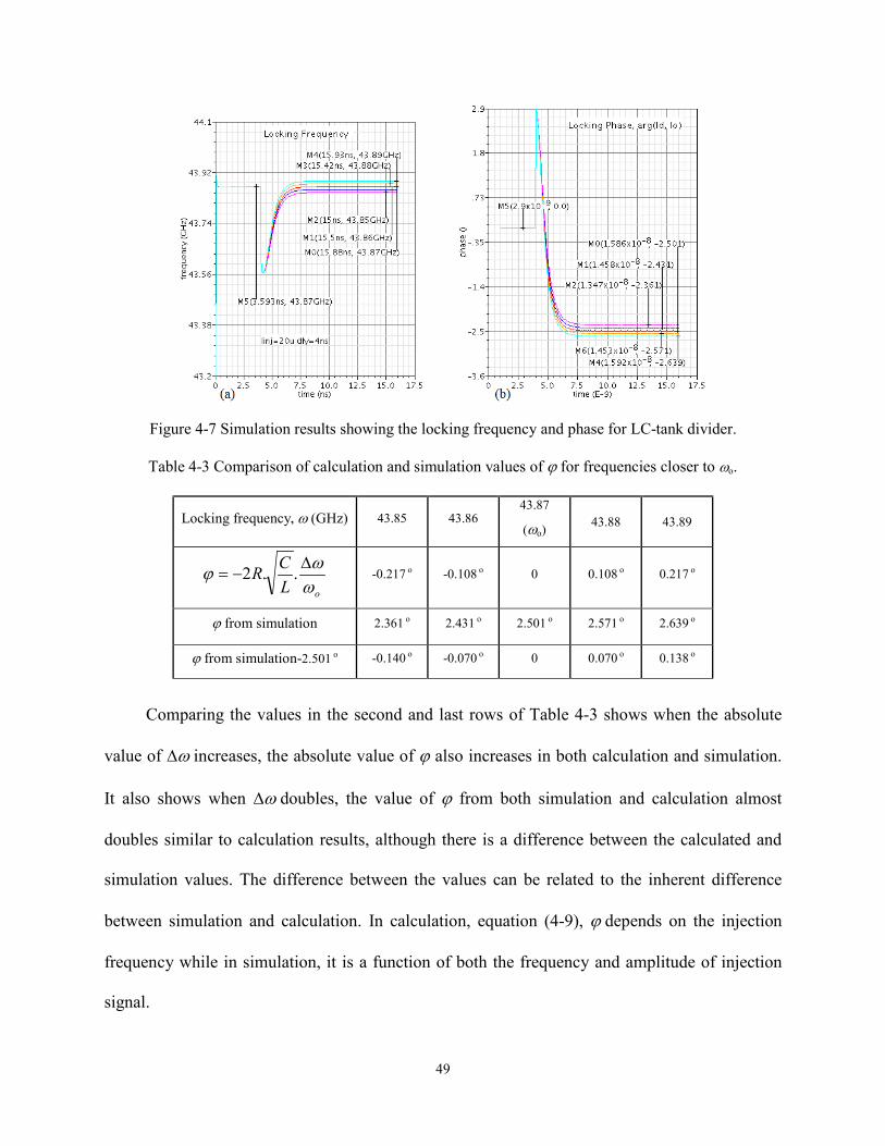
49
Figure 4-7 Simulation results showing the locking frequency and phase for LC-tank divider.
Table 4-3 Comparison of calculation and simulation values of ϕ for frequencies closer to ωo.
Comparing the values in the second and last rows of Table 4-3 shows when the absolute
value of ∆ω increases, the absolute value of ϕ also increases in both calculation and simulation.
It also shows when ∆ω doubles, the value of ϕ from both simulation and calculation almost
doubles similar to calculation results, although there is a difference between the calculated and
simulation values. The difference between the values can be related to the inherent difference
between simulation and calculation. In calculation, equation (4-9), ϕ depends on the injection
frequency while in simulation, it is a function of both the frequency and amplitude of injection
signal.
Locking frequency, ω (GHz) 43.85 43.86 43.87
(ωo) 43.88 43.89
oLCR
ωωϕ ∆
−= ..2 -0.217 o -0.108 o 0 0.108 o 0.217 o
ϕ from simulation 2.361 o 2.431 o 2.501 o 2.571 o 2.639 o
ϕ from simulation-2.501 o -0.140 o -0.070 o 0 0.070 o 0.138 o

50
Table 4-4 shows the value of ϕ from simulation results is a function of both the frequency
and amplitude of injection signal.
Table 4-4 Simulation results for different frequency and amplitude values of injected signal.
Analyzing the values in Table 4-4, points out the difference between calculation and
simulation results. Despite the independence of the calculation values to the injection amplitude,
the simulation results for the same ∆ω with different injection amplitudes are not the same. For
instance, the value of ϕ from simulation for ω=43.77GHz are -1.62o, -0.88o and -0.06o when
injection amplitudes of 20uA, 15uA and 10uA respectively while the calculation value for the
same frequencies from Table 4-2 is -1.084 o without any dependencies to injection amplitude.
4.2 CML Ring Frequency Divider
Similar to LC-tank frequency divider, for simplicity of the analysis a differential current at
half-rate frequency is injected to the output nodes as shown in Figure 4-8, instead of injecting the
signal via the clock voltage inputs at full-rate frequency.
iinj
20uA 15uA 10uA 5uA 0uA
ω
43.67GHz ϕ=0.28 o
43.72GHz ϕ=1.02 o ϕ=0.18 o
43.77GHz ϕ=1.62 o ϕ=0.88o ϕ=0.06 o
43.82GHz ϕ=2.11 o ϕ=1.42 o ϕ=0.73 o ϕ=0.2 o
43.87GHz (ωo) ϕ=2.51 o ϕ=1.82 o ϕ=1.18 o ϕ=0.53 o ϕ=0
43.92GHz ϕ=2.8 o ϕ=2.11 o ϕ=1.46 o ϕ=0.77 o
43.97GHz ϕ=2.99 o ϕ=2.28 o ϕ=1.54 o
44.02GHz ϕ=3.03 o ϕ=2.3 o
44.07GHz ϕ=3.06 o

51
Figure 4-8 Schematic of the ring frequency divider with current injected to output nodes.
Figure 4-9 (a) Equivalent circuit, (b) Block diagram and (c) Vector representation for ring divider.
The circuit shown in Figure 4-8 can be modeled as shown in Figure 4-9. An equivalent
circuit corresponding to the first stage of an n-stage ring (driven by the output Vo of the last
stage) is shown in Figure 4-9(a) where iinj is the injected current, id is the feedback current which
is the drain buffer current of the first stage, and their sum is, io = id + iinj which goes to the total
load of the first stage. The block diagram form is shown in Figure 4-9(b). A vector representation
of the three currents is shown in Figure 4-9(c) where the locking phase ϕ is the angle between
the feedback current, id and the sum current, io, and phase θ is the angle between the feedback
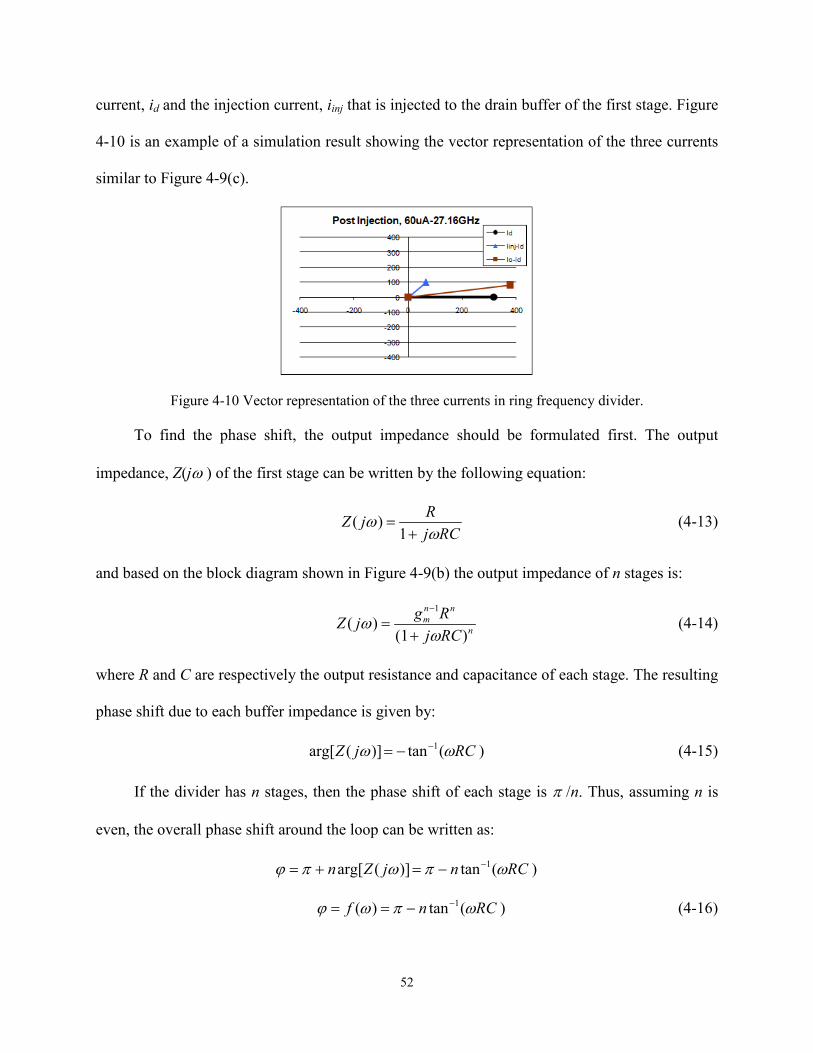
52
current, id and the injection current, iinj that is injected to the drain buffer of the first stage. Figure
4-10 is an example of a simulation result showing the vector representation of the three currents
similar to Figure 4-9(c).
Figure 4-10 Vector representation of the three currents in ring frequency divider.
To find the phase shift, the output impedance should be formulated first. The output
impedance, Z(jω ) of the first stage can be written by the following equation:
RCjRjZω
ω+
=1
)( (4-13)
and based on the block diagram shown in Figure 4-9(b) the output impedance of n stages is:
n
nnm
RCjRgjZ
)(1)(
1
ωω
+=
−
(4-14)
where R and C are respectively the output resistance and capacitance of each stage. The resulting
phase shift due to each buffer impedance is given by:
) (tan )](arg[ 1 RCjZ ωω −−= (4-15)
If the divider has n stages, then the phase shift of each stage is π /n. Thus, assuming n is
even, the overall phase shift around the loop can be written as:
) (tan )](arg[ 1 RCnjZn ωπωπϕ −−=+=
) (tan)( 1 RCnf ωπωϕ −−== (4-16)
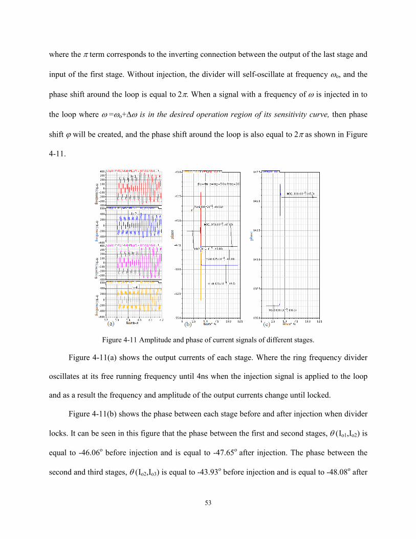
53
where the π term corresponds to the inverting connection between the output of the last stage and
input of the first stage. Without injection, the divider will self-oscillate at frequency ωo, and the
phase shift around the loop is equal to 2π. When a signal with a frequency of ω is injected in to
the loop where ω =ωo+∆ω is in the desired operation region of its sensitivity curve, then phase
shift ϕ will be created, and the phase shift around the loop is also equal to 2π as shown in Figure
4-11.
Figure 4-11 Amplitude and phase of current signals of different stages.
Figure 4-11(a) shows the output currents of each stage. Where the ring frequency divider
oscillates at its free running frequency until 4ns when the injection signal is applied to the loop
and as a result the frequency and amplitude of the output currents change until locked.
Figure 4-11(b) shows the phase between each stage before and after injection when divider
locks. It can be seen in this figure that the phase between the first and second stages, θ (Io1,Io2) is
equal to -46.06o before injection and is equal to -47.65o after injection. The phase between the
second and third stages, θ (Io2,Io3) is equal to -43.93o before injection and is equal to -48.08o after
54
injection. The phase between the third and fourth stages, θ (Io3,Io4) is equal to -46.06o before
injection and is equal to -49.06o after injection. Figure 4-11(c) shows the phase between the
fourth and first stages, θ (Io4,Io1) is equal to 136.1o before injection and is equal to 145.3o after
injection. The sum of all phases before injection is equal to -46.06o + -43.93o +-46.06o +136.1o =
0.05o ≅ 0 and the sum of all phases after injection is also equal to -47.65o+ -48.08o + -49.6o
+145.3o = 0.03o ≅ 0. The sums are almost zero. This result verify that the phase shift around the
loop after injection is also equal to 2π , although the phases between the individual stages have
been changed due to the injection.
The phase shift ϕ = ƒ(ω) is a function of ω. The Taylor expansion of ƒ(ω) around ωo is:
...))(())(()()( 2 +−′′+−′+== ooooo ffff ωωωωωωωωϕ (4-17)
knowing that
)(tan)( 1 RCnf oo ωπω −−=
which is the phase shift at the self-oscillation frequency and is equal to zero.
We have dxdu
uu
dxd
21
11tan
+=− and assuming u = ωoRC, then the first and second-order
polynomials of the Taylor expansion would be:
)()(1
))(( 2 oo
oo RCnRCf ωωω
ωωω −+
−=−′ (4-18)
and
222
32 )(
])(1[)(2))(( o
o
ooo RC
RCnf ωωωωωωω −
+−=−′′ (4-19)
We know that the phase shift around the loop at self-oscillation frequency for n-stage ring
oscillator is π = n×tan-1(ωoRC), therefore for the 4-stage CML ring oscillator, we have:
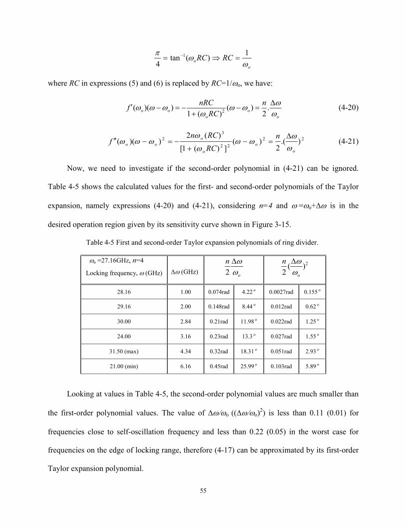
55
oo RCRC
ωωπ 1)(tan
41 =⇒= −
where RC in expressions (5) and (6) is replaced by RC=1/ωo, we have:
oo
ooo
nRC
nRCfω
ωωωω
ωωω ∆=−
+−=−′ .
2)(
)(1))(( 2 (4-20)
2222
32 ).(
2)(
])(1[
)(2))((
oo
o
ooo
nRCRCn
fω
ωωω
ω
ωωωω
∆=−
+−=−′′ (4-21)
Now, we need to investigate if the second-order polynomial in (4-21) can be ignored.
Table 4-5 shows the calculated values for the first- and second-order polynomials of the Taylor
expansion, namely expressions (4-20) and (4-21), considering n=4 and ω =ωo+∆ω is in the
desired operation region given by its sensitivity curve shown in Figure 3-15.
Table 4-5 First and second-order Taylor expansion polynomials of ring divider.
ωo =27.16GHz, n=4
Locking frequency, ω (GHz)
∆ω (GHz) o
nω
ω∆2
2)(2 o
nω
ω∆
28.16 1.00 0.074rad 4.22 o 0.0027rad 0.155 o
29.16 2.00 0.148rad 8.44 o 0.012rad 0.62 o
30.00 2.84 0.21rad 11.98 o 0.022rad 1.25 o
24.00 3.16 0.23rad 13.3 o 0.027rad 1.55 o
31.50 (max) 4.34 0.32rad 18.31 o 0.051rad 2.93 o
21.00 (min) 6.16 0.45rad 25.99 o 0.103rad 5.89 o
Looking at values in Table 4-5, the second-order polynomial values are much smaller than
the first-order polynomial values. The value of ∆ω/ωo ((∆ω/ωo)2) is less than 0.11 (0.01) for
frequencies close to self-oscillation frequency and less than 0.22 (0.05) in the worst case for
frequencies on the edge of locking range, therefore (4-17) can be approximated by its first-order
Taylor expansion polynomial.

56
...))(()()( +−′+== ooo fff ωωωωωϕ
)()(1
)(tan)( 21
oo
o RCnRCRCnf ωω
ωωπω −
+−
+−= − (4-22)
Therefore, the phase difference due to the injected signal is:
ωω
ϕ ∆+
−≈ 2)(1 RCnRC
o
(4-23)
Using an argument similar to LC-tank , from Figure 4-9(c) we can write:
θ
θθ
θϕ
cos1
sin.cos
sintan
d
injd
inj
injd
inj
iii
iii
i
+=
+= (4-24)
Similar to LC- tank, we need to investigate the correctness of assuming ϕ is equal to tanϕ.
Table 4-6 shows the value for the first-order polynomials of expression (4-20), ϕ and tanϕ
for locking frequencies.
Table 4-6 Comparison of the values of first-order polynomial, ϕ and tanϕ.
Table 4-6 shows that we can assume ϕ and tanϕ are equal for frequencies close to the self-
oscillation frequency and within 6.7% in the worst case, for frequencies close to the edge of
locking range. Though, we should be careful to generalize this assumption. In this case,
equations (10) and (11) could be combined, therefore we have:
Locking frequency, ω (GHz) 28.16 29.16 30 24 31.5
(max)
21
(min)
∆ω (GHz) 1 2 2.84 3.16 4.34 6.16
oωωϕ ∆
= .2 (rad) 0.074 0.148 0.21 0.23 0.32 0.45
tanϕ 0.074 0.148 0.21 0.23 0.33 0.48
Error 0% 0% 0% 0% 3.125% 6.67%

57
θ
θωθω cos1
sin.)()(1 2
d
injd
injo
o
iii
idtd
RCnRC
+=∆−
+− (4-25)
Consequently, the differential equation is:
o
d
injd
injo
iii
inRC
RCdtd ω
θ
θωθ∆+
+
+−=
cos1
sin..)(1 2
(4-26)
for n stages. If we consider the case with m points that signals at full-rate frequency are injected
to the divider, then the expression in (4-26) should be modified to:
o
d
injd
injo
iini
miRC
RCdtd ω
θ
θωθ∆+
+
+−=
cos1
sin..)(1 2
(4-27)
Equation (4-27) implies: 1) The derivative of θ with respect to time, dθ/dt, depends not
only on the injection ratio Iinj/Id, but also to the product of the self-oscillation frequency and the
RC time constant. Normally this product is constant for a given value of n. For the divider shown
in Figure 4-8, it is normal to apply two points of injection, m=2 by applying a differential signal.
2) When dθ/dt is equal to zero, the divider is locked.
4.2.1 Validating Calculation of ϕ by Simulation Results for Ring Divider
Now, we need to verify the calculated values of ϕ by the simulation result. Figure 4-12
shows the locking frequency and the locking phase when a 50uA current, Iinj with half-rate
frequency is injected to the drain buffer of the first and the third stages, as shown in Figure 4-8.
ω is in the desired operation region of frequency divider's sensitivity curve.

58
Figure 4-12 Simulation results showing locking frequency and phase for ring divider.
Table 4-7 Comparison of calculation and simulation values of ϕ for ring divider.
Figure 4-12(a) shows the simulations results for ring frequency divider which is in free
running at frequency of 27.16GHz until 4ns and a 50uA current with frequencies of 25.16-,
26.16-, 27.16-, 28.16-, and 29.16-GHz is injected with a starting time of 4ns. The ring frequency
divider locks at the injected frequency after few cycles. Figure 4-12(b) shows the locking phase,
ϕ between the drain buffer current, id1 and the current which goes to the total load, io1 for the
first stage corresponding to the injection frequencies. The phase values shown in Figure 4-12(b)
have units of degree.
Locking frequency, ω(GHz) ,
Iinj=50uA 25.16 26.16
27.16
(ωo) 28.16 29.16
oωωϕ ∆
×= 2 -8.44 o -4.22 o 0 4.22 o 8.44 o
ϕ from simulation 3.455 o 7.503 o 10.51o 12.76 o 14.32 o
ϕ from simulation-10.51o -7.055 o -3.007 o 0 2.21 o 3.71 o

59
Table 4-7 shows the locking phase, ϕ corresponding to locking frequencies from the
calculation and simulation. The simulation value of ϕ, the third row in Table 4-7, is not equal to
zero at self-oscillation similar to the calculated value in the second row. One of the reasons could
be because the simulation value of ϕ is a function of both the frequency and amplitude of
injection signal. Similar to the LC-based divider, for better comparison of the calculated and
simulated values, the simulation values are subtracted from the self-oscillation value (10.51o).
These latter values are shown in the last row of Table 4-7.
Comparing the values in the second and the last rows of Table 4-7 implies that: 1) when
the absolute value of ∆ω increases, the absolute value of ϕ also increases in both calculation and
simulation, and 2) when the ∆ω value multiplies by two, the value of ϕ almost multiplies by two.
It seems that the simulation results confirm a similar trend as calculation, although the values are
different.
Figure 4-13 Simulation results of injection frequencies very close to ωο.

60
More simulations were done for ωinj values closer to ωo .The injection frequencies are in
the desired operation region of the divider's sensitivity curve. The simulation results are shown in
Figure 4-13. Similar to previous tests, Figure 4-13(a) shows the simulation results of ring
frequency divider which is free running at 27.16GHz until 4ns and a 50uA current is injected at a
starting time of 4ns. The values of injection frequency are 26.96-, 27.06-, 27.16-, 27.26-, and
27.36-GHz. Figure 4-13(b) shows the locking phase, ϕ corresponding to these frequencies.
Table 4-8 Comparison of calculation and simulation values of ϕ for ring divider.
Table 4-8 summarizes the ϕ value from calculation and simulation of the latter tests.
Comparing the values in the second and the last rows of Table 4-8 shows when the absolute value
of ∆ω increases, the absolute value of ϕ also increases in both calculation and simulation. It also
shows when ∆ω doubles, the value of ϕ from both simulation and calculation doubles although
there is a difference between the calculated and simulation values. The difference between the
values is related to the inherent difference between simulation and calculation. In calculation,
ϕ depends on the injection frequency while in simulation, it is a function of both the frequency
and amplitude of injection signal.
Ignoring the differences between the calculated and simulation values , the simulation
results confirm the calculation results for injection frequencies very close to ωο.
Locking frequency, ω(GHz) 26.96 27.06 27.16
(ωo) 27.26 27.36
oωωϕ ∆
= .2 -0.84 o -0.42 o 0 0.42 o 0.84 o
ϕ from simulation 9.98 o 10.25 o 10.51 o 10.77 o 11.02 o
ϕ from simulation-10.51o -0.53 o -0.26 o 0 0.26 o 0.51 o

61
4.3 CML D Flip-Flop Frequency Divider
Similar to LC-tank frequency divider, for simplicity of the analysis a differential current
with half-rate frequency is injected to the output nodes as shown in Figure 4-14, instead of
injecting the signal via the clock voltage inputs at full-rate frequency.
Figure 4-14 Schematic of the DFF frequency divider with current injected to output nodes.
Figure 4-15 (a) Equivalent circuit, (b) Block diagram and (c) Vector representation for the DFF divider.
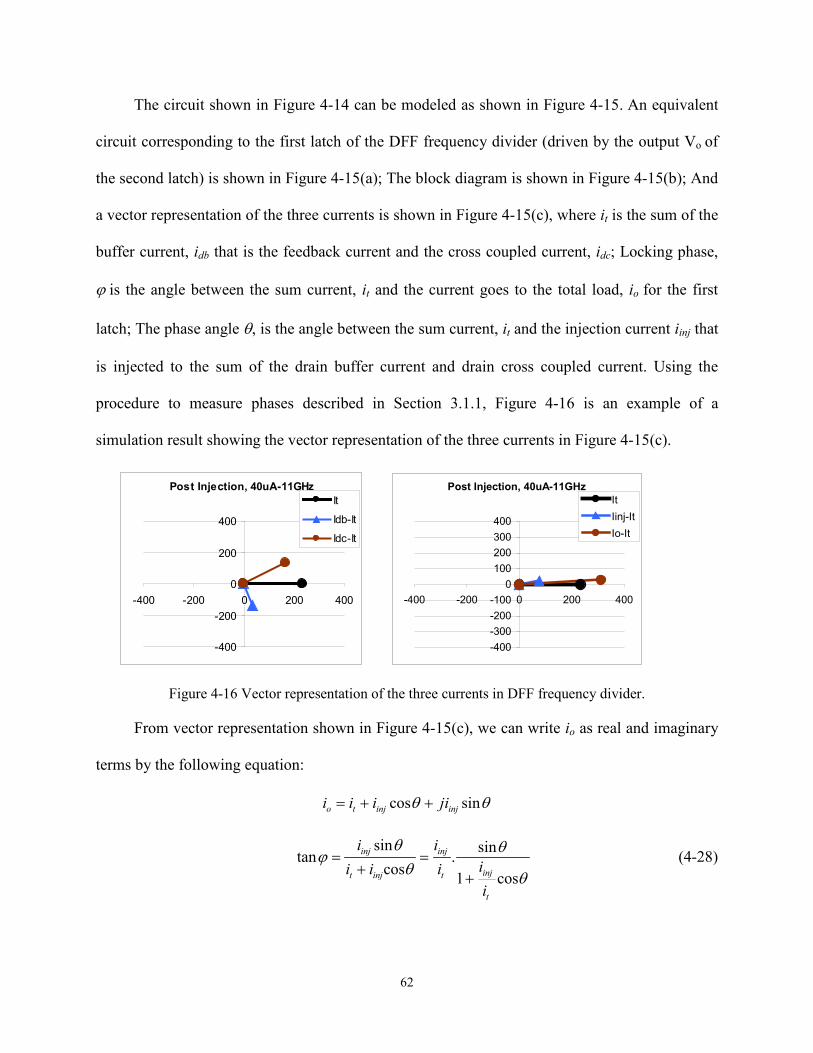
62
The circuit shown in Figure 4-14 can be modeled as shown in Figure 4-15. An equivalent
circuit corresponding to the first latch of the DFF frequency divider (driven by the output Vo of
the second latch) is shown in Figure 4-15(a); The block diagram is shown in Figure 4-15(b); And
a vector representation of the three currents is shown in Figure 4-15(c), where it is the sum of the
buffer current, idb that is the feedback current and the cross coupled current, idc; Locking phase,
ϕ is the angle between the sum current, it and the current goes to the total load, io for the first
latch; The phase angle θ, is the angle between the sum current, it and the injection current iinj that
is injected to the sum of the drain buffer current and drain cross coupled current. Using the
procedure to measure phases described in Section 3.1.1, Figure 4-16 is an example of a
simulation result showing the vector representation of the three currents in Figure 4-15(c).
Post Injection, 40uA-11GHz
-400
-200
0
200
400
-400 -200 0 200 400
It
Idb-It
Idc-It
Post Injection, 40uA-11GHz
-400-300-200-100
0100200300400
-400 -200 0 200 400
ItIinj-ItIo-It
Figure 4-16 Vector representation of the three currents in DFF frequency divider.
From vector representation shown in Figure 4-15(c), we can write io as real and imaginary
terms by the following equation:
θθ sincos injinjto jiiii ++=
θ
θθ
θϕ
cos1
sin.cos
sintan
t
injt
inj
injt
inj
iii
iii
i
+=
+= (4-28)

63
To find phase shift, the output impedance should be found first. The output impedance,
Z(jω) for the first latch can be written as the following equation:
1-1
1.1
)(
−−
−=
RgmCRjRgm
RjZ
c
c ωω (4-29)
where R, C, and gmc are the output resistance, capacitance, and the trans-conductance of the
cross coupled transistors pair, respectively of each latch. Assuming:
11||
−−=
−=
RgmR
gmRR
cceq (4-30)
and then combining equations (4-29) and (4-30), consequently results:
CRjR
jZeq
eq
ωω
+=
1)( (4-31)
The phase shift due to impedance is given by:
) (tan )](arg[ 1 CRjZ eqωω −−= (4-32)
The DFF output impedance is:
2
2
)(1)(
CRjRjZ
eq
eqDFF ω
ω+
= (4-33)
Because the DFF divider has 2 Latches, the phase shift of each latch is π/2. Thus, the
overall phase shift around the loop can be written as:
) (tan2 )](arg[2 1 CRjZ eqωπωπϕ −−=+=
) (2tan-)( -1 CRf eqωπωϕ == (4-34)
where the π term corresponds to the inversion realized by the inverting connection between the
output of the second latch and input of the first latch. Without injection, the divider will self-
oscillate at frequency ωo, and the phase shift around the loop will be 2π. When a signal with the

64
frequency ω is injected in to the loop, assuming the frequency, ω =ωo+∆ω is in the desired
operation region of its sensitivity curve, then the phase shift ϕ will be created, although the phase
shift around the loop will be 2π again.
The phase shiftϕ =ƒ(ω) is a function of ω and the Taylor expansion for ƒ(ω) around ωo
would be:
...))(())(()()( 2 +−′′+−′+== ooooo ffff ωωωωωωωωϕ (4-35)
knowing that
)(tan2)( 1 CRf eqoo ωπω −−= (4-36)
is the phase shift at the self-oscillation frequency.
We have dxdu
uu
dxd
21
11tan
+=− and assume that CRu eqoω= , then :
)()(1
2))(( 2 o
eqo
eqoo CR
CRf ωω
ωωωω −
+−=−′ (4-37)
222
32 )(
])(1[)(4
))(( oeqo
eqooo CR
CRf ωω
ωω
ωωω −+
−=−′′ (4-38)
Now the question is whether or not the second-order polynomial given in (4-38) can be
ignored when compared to the first-order polynomial given in (4-37). To simplify the equations
(4-37) and (4-38), the relationship between time constant, ReqC and self-oscillation frequency, ωo
can be found using Tosc =2n.tp where tp is a propagation delay of each latch and is equal to tp
=0.69× ReqC.
ooeq
po CR
tn ωωω
8.21
69.0221
..21
≅××
=⇒=
By substituting ReqC in the first and the second-order polynomials of the Taylor expansion
given in expressions (4-37) and (4-38), with ReqC =1/(2.8ωo), we have:

65
ooof
ωωωωω ∆
×≅−′ 7.0))(( (4-39)
Table 4-9 shows the calculated values for the first and the second-order polynomials of the
Taylor expansion given in (4-35), considering ω =ωo+∆ω is in the desired operation region given
by its sensitivity curve shown in Figure 3-6.
Table 4-9 First and second-order Taylor expansion polynomials of DFF divider.
0ω =15.18GHz
Locking frequency, ω (GHz)
∆ω (GHz)
))(( oof ωωω −′
=oωω∆
×7.0
2))(( oof ωωω −′′
= 2)(15.0oωω∆
×
16.18 1.00 0.046rad 2.64 o 6.51-04rad 0.037 o
17.18 2.00 0.092rad 5.28 o 2.61-03rad 0.149 o
11.00 4.18 0.193rad 11.04 o 0.012rad 0.651 o
7.00 8.18 0.377rad 21.61 o 0.044rad 2.52 o
19.5 (max) 4.32 0.199rad 11.41 o 0.012rad 0.696 o
2G (min) 13.18 0.868rad 34.8 o 0.113rad 6.49 o
Looking at Table 4-9 values, the second-order polynomial values are within 6% of the
first-order polynomial values for frequencies close to the self-oscillation frequency and less than
18% in the worst case, for frequencies close to the edge of locking range. Therefore, the Taylor
expansion in (4-35) can be approximated by its first-order polynomial.
...))(()()( +−′+== ooo fff ωωωωωϕ
)()(1
2)(tan2)( 2
1o
eqo
eqo CR
CRRCf ωω
ωωπω −
+−
+−= − (4-40)
As a result, the phase difference due to the injected signal is:

66
ωω
ϕ ∆+
−≈ 2)(12
CRCR
eqo
eq (4-41)
Now, we need to investigate the correctness of assuming ϕ is equal to tanϕ. Table 4-10
shows the value of ϕ in equation (4-41), and tanϕ for different values of injection frequencies, ω
where ω =ωo+∆ω is in the desired operation region given by the divider's sensitivity curve shown
in Figure 3-6.
Table 4-10 Comparison of the values of first-order polynomial, ϕ and tanϕ for DFF divider.
Table 4-10 shows that we can assume ϕ and tanϕ to be equal for the injection frequencies
which are close to the self-oscillation frequency, the first few columns from left, but the
difference widens up as ∆ω increases. This is due to the fact that the desired operation region in
sensitivity curve for DFF divider is very wide, and the approximation of tanϕ being equal to ϕ
cannot be generalized for all injection frequencies in the desired operation region of sensitivity
curve.
4.3.1 Validating Calculation of ϕ by Simulation Results for DFF Divider
The next step is to see whether or not the calculated value forϕ is matching the simulation
result. Table 4-11 summarizes the calculation and simulations results for DFF frequency divider
which is in the self-oscillation frequency of 15.18GHz until 4ns, and a 40uA current with
Locking frequency, ω (GHz) 16.18 17.18 11.0 7.0 19.0 2.0
∆ω (GHz) 1G 2 4.18 8.18 4.32 13.18
oωωϕ ∆
×= 7.0 (rad) 0.046 0.092 0.193 0.377 0.199 0.868
tanϕ (rad) 0.046 0.092 0.195 0.395 0.202 1.18
Error 0% 0% 1.04% 4.77% 1.5% 35.9%

67
frequencies of 7-, 11-, 13.18-, 14.18-, 15.18-, 16.18-, 17.18-, and 19-GHz is injected starting at
4ns. The DFF frequency divider locks at the injected frequency after a few cycles. The locking
phase, ϕ is the phase between it1 and the current that goes to the total load, io1 corresponding to
the injected frequencies for the first latch. The injected frequencies are in the desired frequency
divider operation region.
Table 4-11 Comparison of calculation and simulation values of ϕ for DFF divider when Iinj=40uA.
As mentioned earlier, the simulated values are dependent on the amplitude of the injected
signal. This might be one of the reasons why the value of ϕ from simulation, the third row in
Table 4-11, is not equal to zero at self-oscillation similar to the calculated value in the second
row. In order to better comparison of the calculated and simulated values, the simulation value is
subtracted from its self-oscillation value (12.77o). This latter value is shown in the last row of
Table 4-11.
Comparing the values in the second and the last rows of Table 4-11 shows when the
absolute value of ω∆ increases, the absolute value of ϕ also increases in both calculation and
simulation, in the other word shows the calculation follows the same trend as simulation result.
The values in the table show when the absolute value of ∆ω >1GHz (∆ω/ωo≅0.07 ), the
difference between simulated and calculated values of ϕ gets bigger than 4% (23%) on the
negative (positive) values of ∆ω.
Locking frequency, ω(GHz)
Iinj=40uA 7.0 11.0 13.18 14.18
15.18
(ωo) 16.18 17.18 19.0
ϕ =0.7×(∆ω/ωo) -21.67 o -11.04 o -5.28 o -2.64 o 0 2.64 o 5.28 o 11.41 o
ϕ from simulation -57.32o -5.42o 7.11o 10.25 o 12.77o 14.90o 16.75 o 19.90 o
ϕ from simulation -12.77o -70.09o -18.19 o -5.66 o -2.52 o 0 2.13 o 3.98 o 5.13 o

68
Table 4-11 values are for the injection amplitude of 40uA where the desired operation
region of sensitivity curve is wide and covers a wide range of frequencies. Since the simulation
results convey that the model matches better for the injection signal frequencies closer to self-
oscillation frequency, one way to evaluate this, would be to lower the injection signal amplitude
where the desired operation region of sensitivity curve becomes narrower. Following are the
results when injection current amplitude is 10uA and 5uA.
When the injection current amplitude is 10uA, the desired operation region of sensitivity
curve is narrower. The injected frequencies chosen for simulation are 13.68-, 14.18-, 14.68-,
15.18-, 15.68-, 16.18-, and 16.68-GHz with the starting time of 4ns. Table 4-12 summarizes the
calculation and simulation results when Iinj=10uA.
When the injection current amplitude is 5uA, the desired operation region of sensitivity
curve gets even more narrower. The injected frequencies chosen for simulation are 14.48-,
14.68-, 14.98-, 15.18-, 15.38-, 15.68-, and 15.88-GHz.
Table 4-12 Comparison of calculation and simulation values of ϕ for DFF divider when Iinj=10uA.
Table 4-13 Comparison of calculation and simulation values of ϕ for DFF divider when Iinj=5uA.
Locking frequency, ω(GHz)
Iinj=10uA 13.68 14.18 14.68
15.18
(ωo) 15.68 16.18 16.68
ϕ =0.7×(∆ω/ωo) -3.96 o -2.64 o -1.32 o 0 1.32 o 2.64 o 3.96 o
ϕ from simulation -4.17o 0.42o 2.85 o 4.51o 5.69o 6.48 o 7.01 o
ϕ from simulation -4.51o -8.68 o -4.09 o -1.67 o 0 1.18 o 1.97 o 2.50 o
Locking frequency, ω(GHz)
Iinj=5uA 14.48 14.68 14.98
15.18
(ωo) 15.38 15.68 15.88
ϕ =0.7×(∆ω/ωo) -1.85 o -1.32 o -0.53 o 0 0.53 o 1.32 o 1.85 o
ϕ from simulation -0.84o 0.52o 1.87 o 2.52o 3.01o 3.49o 3.63o
ϕ from simulation -2.52o -3.36 o -1.99 o -0.65 o 0 0.50 o 0.98 o 1.11 o

69
Results in Table 4-11, Table 4-12, and Table 4-13 validate when the absolute value of ∆ω
increases the absolute value of ϕ also increases in both calculation and simulation, but the values
are different between calculation and simulation.
Analyzing the values in Table 4-11, Table 4-12, and Table 4-13, also points out another
difference between calculations and simulation results. Despite the independence of the
calculation values to the injection amplitude, the simulation results for the same ∆ω with
different injection amplitudes are not the same. For instance, the ϕ from simulation for
ω=14.68GHz in Table 4-12, and Table 4-13 are -1.67o and -1.99o respectively as opposed to their
calculation values being -1.32 o for both cases.
Summarizing the findings in Table 4-11, Table 4-12, and Table 4-13, it can be noted that
the calculation values for ϕ depend on the injection frequency but the measured values of ϕ from
simulation, are a function of both frequency and amplitude of injection signal. This is in
accordance with the findings for LC-tank and ring frequency dividers that were previously
presented.
It should be noted that for small values of ∆ω the assumption of ϕ being equal to tanϕ is
valid for DFF frequency divider. As a result, equations (4-28) and (4-41) could be combined and
with the same argument that have been done for LC-tank and ring frequency dividers, we can
write:
θ
θωθω cos1
sin.)()(1
22
t
injt
injo
eqo
eq
iii
idtd
CRCR
+=∆−
+− (4-42)
The resulting differential equation is:

70
o
t
injt
inj
eq
eqo
iii
iCR
CRdtd ω
θ
θωθ∆+
+
+−=
cos1
sin..2
)(1 2
(4-43)
As mentioned earlier, this is only valid when the injections amplitude is very low and the
injection frequency is very close to self-oscillation frequency.

71
CHAPTER 5. SUMMARY AND CONCLUSIONS
In this thesis, three high-speed dividers, the LC-tank frequency divider, the CML ring
frequency divider, and the CML DFF frequency divider with negative feedback, are analyzed
based on a defined condition for injection locking. Based on the model of each topology and the
concept of injection locking, the instantaneous and locking phase equations are mathematically
formulated.
It should be noted that for the case of DFF frequency divider because of its very wide
desired operation region, the derived equations are mainly valid either for lower injection
amplitudes where the desired operation region of its sensitivity curve is relatively narrow or
injection frequencies very close to its self-oscillation frequency regardless of injection amplitude.
The analytical results are compared with the simulation results utilizing a novel procedure
that is developed to measure locking phase, instantaneous phase, or the phase between any two
signals. This procedure provides a good ability to better understand the behavior of the divider
under an impressed signal.
Regarding the locking phase, the simulation results follow a similar trend as the derived
equations for all three topologies although the absolute values are different. The difference
between the values can be related to the inherent difference between simulation and calculation.
In calculation, locking phase ϕ depends on the injection frequency while in simulation, it is
observed to be a function of both the frequency and amplitude of injection signal.
In summary, considering the locking phase as a function of both frequency and amplitude
of the injection signal, opens a new chapter in this area of research.

72
REFERENCES
[1] X. Gui, Z. Chen, and M. M. Green, “Analysis of Nonlinearities in Injection-Locked
Frequency Dividers,” IEEE Transactions On Microwave Theory and Techniques, vol. 63, no.
3, pp. 945-953, Mar. 2015.
[2] X. Gui, and M. M. Green, “Nonlinearities in Frequency Dividers,” 20th European Conference
on Circuit Theory and Design (ECCTD), pp. 532-535, Aug. 2011.
[3] U. Singh, and M. M. Green, “High-frequency CML clock dividers in 0.13-μm CMOS
operating up to 38 GHz,” IEEE Journal of Solid-State Circuits, vol. 40, no. 8, pp. 1658-1661,
Aug. 2005.
[4] R. Adler, “A study of locking phenomena in oscillators,” Proceedings of the IEEE, vol. 61,
no. 10, pp. 1380–1385, Oct. 1973.
[5] L. J. Paciorek, “Injection locking of oscillators,” Proceedings of the IEEE, vol. 53, no. 11,
pp. 1723–1727, Nov. 1965.
[6] B. Razavi, “A study of Injection locking and pulling in oscillators,” IEEE Journal of Solid-
State Circuits, vol. 39, no. 9, pp. 1415–1424, Sept. 2004.
[7] K. Sengupta, and H. Hashemi, “Maximum frequency of operation of CMOS Static
Frequency Dividers: Theory and Design techniques,” 13th IEEE International Conference on
Electronics, Circuits and Systems (ICECS), pp. 584-587, Dec. 2006.
[8] A. Mirzaei, M. E. Heidari, R. Bagheri, S. Chehrazi, and A. A. Abidi, “Injection-locked
frequency dividers based on ring oscillators with optimum injection for wide lock range,”
Symposium on VLSI Circuits, pp. 174–175, Jun. 2006

73
[9] P. Heydari and R. Mohanavelu, “Design of Ultrahigh-Speed Low-Voltage CMOS CML
Buffers and Latches,” Proceedings of the 2003 International Symposium on Circuits and
Systems (ISCAS), vol. 2, pp. 208-211, May 2003.
[10] Prof. M. M. Green, “EECS 270C / UCI,” Winter 2013.
[11] H. Knapp, H. D. Wohlmuth, M. Wurzer, and M. Rest, "25 GHz static frequency divider
and 25 Gb/s multiplexer in 0.12μm CMOS," IEEE International Solid-State Circuits
Conference, 2002. Digest of Technical Papers. ISSCC., vol. 1, pp. 302-468, Feb. 2002.