LECTURE 170 – APPLICATIONS OF PLLS AND FREQUENCY...
21
Lecture 170 - Frequency Synthesizers - I (6/25/03) Page 170-1 ECE 6440 - Frequency Synthesizers © P.E. Allen - 2003 LECTURE 170 – APPLICATIONS OF PLLS AND FREQUENCY DIVIDERS (PRESCALERS) (References [2, 3, 4, 6, 11]) Objective The objective of this presentation is: 1.) Examine the applications of PLLs 2.) Develop and characterize the techniques used for frequency division Outline • Applications of PLLs • Integrated Circuit Frequency Synthesizers – Architectures and Techniques • Dividers for Frequency Synthesizers • Noise-Shaping Techniques • Summary Lecture 170 - Frequency Synthesizers - I (6/25/03) Page 170-2 ECE 6440 - Frequency Synthesizers © P.E. Allen - 2003 APPLICATIONS OF PLLS The PLL The PLL is a very versatile building block and is suitable for a variety of applications including: 1.) Demodulation and modulation 2.) Signal conditioning 3.) Frequency synthesis 4.) Clock and data recovery 5.) Frequency translation
Transcript of LECTURE 170 – APPLICATIONS OF PLLS AND FREQUENCY...

Lecture 170 - Frequency Synthesizers - I (6/25/03) Page 170-1
ECE 6440 - Frequency Synthesizers © P.E. Allen - 2003
LECTURE 170 – APPLICATIONS OF PLLS AND FREQUENCYDIVIDERS (PRESCALERS)
(References [2, 3, 4, 6, 11])ObjectiveThe objective of this presentation is:1.) Examine the applications of PLLs2.) Develop and characterize the techniques used for frequency divisionOutline• Applications of PLLs• Integrated Circuit Frequency Synthesizers – Architectures and Techniques• Dividers for Frequency Synthesizers• Noise-Shaping Techniques• Summary
Lecture 170 - Frequency Synthesizers - I (6/25/03) Page 170-2
ECE 6440 - Frequency Synthesizers © P.E. Allen - 2003
APPLICATIONS OF PLLSThe PLLThe PLL is a very versatile building block and is suitable for a variety of applicationsincluding:1.) Demodulation and modulation2.) Signal conditioning3.) Frequency synthesis4.) Clock and data recovery5.) Frequency translation

Lecture 170 - Frequency Synthesizers - I (6/25/03) Page 170-3
ECE 6440 - Frequency Synthesizers © P.E. Allen - 2003
FM DemodulationWhen the PLL is locked on a frequency modulated signal, the controlling voltage to theVCO becomes proportional to the frequency.
PhaseDetector
LoopFilter
VCO
PostdetectionFilter
vin vout
vc
t
vin
t
vout
f1 f2 f1
V2
V1Fig. 4.1-01
Can be used for frequency shift keying (FSK) if a voltage discriminator is placed at theoutput.
Lecture 170 - Frequency Synthesizers - I (6/25/03) Page 170-4
ECE 6440 - Frequency Synthesizers © P.E. Allen - 2003
FM Demodulation – Example
If Ko = 2π(1kHz/Volt), Kv = 500 (sec-1) and ωo = 1000π rads/sec (fo = 500Hz) for theFM demodulator on the previous slide,(a.) Find Vo for fi = 250Hz and 1000Hz.
(b.) What is the time constant of Vo for a step change between these two frequencies?
Solution(a.) We know that
ωosc = ωi = ωo +KoVo → Vo = ωi - ωo
Ko
∴ Vo(250Hz) = 250-500
1000 = -0.25V
Vo(1000Hz) = 1000-500
1000 = +0.5V
(b.) τ = 1
Kv = 2ms
We note that the risetimes of the square wave on the previous page would no longer bezero but take about 10ms to go from one level to another.

Lecture 170 - Frequency Synthesizers - I (6/25/03) Page 170-5
ECE 6440 - Frequency Synthesizers © P.E. Allen - 2003
FM Demodulator – Example –ContinuedExample:
For the PLL of the previous example, find vo(t) if the input signal is frequencymodulated so that
ωi(t) = 2π(500Hz)[1+0.1sin(2πx102)t].
SolutionVo(jω)ωi(jω) =
1Ko
Kv
Kv + jω = 1
Ko
Kv
Kv + j2πx100|
ω=200π
= 1
2000π
500
500+j628 = 1
2000π(0.39-j0.48)
|ωi(jω)| = 0.1(1000π) = 100π = 50(2π)
∴ Vo(jω) = 50
1000(0.39-j0.48) = 50
1000 0.62/-51° = 0.031/-51°
or
vo(t) = 0.031 sin[(2πx102)-51°]
Lecture 170 - Frequency Synthesizers - I (6/25/03) Page 170-6
ECE 6440 - Frequency Synthesizers © P.E. Allen - 2003
Phase ModulatorWhen the PLL is locked on a fixed frequency, a slowly varying signal, vm(t), can be usedto cause the phase shift of the VCO to shift achieving a phase modulator.
PhaseDetector
LoopFilter
voutvcVCO
fref
Fig. 4.1-025
Phasemodulation
signal
vm(t)
vout(t) = Vout cos[ωreft + θm(t)]
where
θm(t) = 1
Kd v m(t)

Lecture 170 - Frequency Synthesizers - I (6/25/03) Page 170-7
ECE 6440 - Frequency Synthesizers © P.E. Allen - 2003
Signal ConditioningThe PLL can operate as a narrowband filter with an extremely high Q to select a desiredsignal in the presence of undesired signals.
PhaseDetector
LoopFilter VCO
vin voutvc
ωcωc
Fig. 4.1-02
This application represents a tradeoff in the capture range and the loop bandwidth.• If the loop bandwidth is small, the SNR of the output can be much greater than the
input.• If the loop bandwidth is large, the capture range for the desired signal is larger (can
track the desired signal better).
Lecture 170 - Frequency Synthesizers - I (6/25/03) Page 170-8
ECE 6440 - Frequency Synthesizers © P.E. Allen - 2003
Frequency SynthesisDividers placed in the feedback and/or input allow the generation of frequencies based ona stable reference frequency.
PhaseDetector÷M
LoopFilter VCO
÷N
fref
Mfref
Mfref = N
fLO
NfLO
fout = MN fref
Voltage which makes
Oscillatorcontrol voltage
Fig. 4.1-03A
When the phase detector is locked, the two incoming frequencies are equal. Therefore,frefM =
foutN ⇒ fout =
NM fref

Lecture 170 - Frequency Synthesizers - I (6/25/03) Page 170-9
ECE 6440 - Frequency Synthesizers © P.E. Allen - 2003
Clock and Data RecoveryThe function of a clock and data recovery circuit is to produce a stable timing signal froma stream of binary data. Clock recovery consists of two basic functions:1.) Edge detection2.) Generation of a stable periodic output
PhaseDetector
LoopFilter
ClockvcEdgeDetector
VCODin
Fig. 4.1-04
Lecture 170 - Frequency Synthesizers - I (6/25/03) Page 170-10
ECE 6440 - Frequency Synthesizers © P.E. Allen - 2003
Jitter SuppressionIn digital communications, transmitter or retrieved data may suffer from timing jitter. APLL clock recovery circuit can be used to regenerate the signal and eliminate the jitter asshown below.
Clock RecoveryCircuit
D QClk
D Flipflop
Din Dout
Fig. 4.1-05
t
t
t
Din
Clock
Dout
Lecture 170 - Frequency Synthesizers - I (6/25/03) Page 170-11
ECE 6440 - Frequency Synthesizers © P.E. Allen - 2003
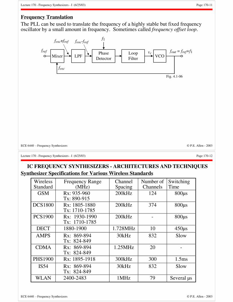
Frequency TranslationThe PLL can be used to translate the frequency of a highly stable but fixed frequencyoscillator by a small amount in frequency. Sometimes called frequency offset loop.
PhaseDetector
LoopFilter
fout = fref+f1vcLPFMixer VCO
fref
Fig. 4.1-06
fosc±fref fosc-freff1
fosc
Lecture 170 - Frequency Synthesizers - I (6/25/03) Page 170-12
ECE 6440 - Frequency Synthesizers © P.E. Allen - 2003
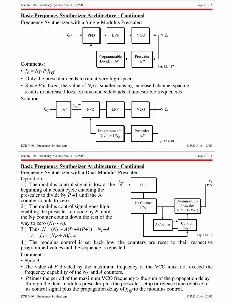
IC FREQUENCY SYNTHESIZERS - ARCHITECTURES AND TECHNIQUESSynthesizer Specifications for Various Wireless Standards
WirelessStandard
Frequency Range(MHz)
ChannelSpacing
Number ofChannels
SwitchingTime
GSM Rx: 935-960Tx: 890-915
200kHz 124 800µs
DCS1800 Rx: 1805-1880Tx: 1710-1785
200kHz 374 800µs
PCS1900 Rx: 1930-1990Tx: 1710-1785
200kHz - 800µs
DECT 1880-1900 1.728MHz 10 450µsAMPS Rx: 869-894
Tx: 824-84930kHz 832 Slow
CDMA Rx: 869-894Tx: 824-849
1.25MHz 20 -
PHS1900 Rx: 1895-1918 300kHz 300 1.5msIS54 Rx: 869-894
Tx: 824-84930kHz 832 Slow
WLAN 2400-2483 1MHz 79 Several µs

Lecture 170 - Frequency Synthesizers - I (6/25/03) Page 170-13
ECE 6440 - Frequency Synthesizers © P.E. Allen - 2003
Components of a Frequency SynthesizerFunction of a frequency synthesizer is to generate a frequency fo from a referencefrequency fref.
Block diagram:
Components: Phase/frequencydetector outputs asignal that is proportional to the difference between the frequency/phase of two inputperiodic signals. The low-pass filter is use to reduce the phase noise and enhance the spectral purity of theoutput.The voltage-controlled oscillator takes the filtered output of the PFD and generates anoutput frequency which is controlled by the applied voltage.The divider scales the output frequency by a factor of N.
fref = foN → fo = Nfref
Phase FrequencyDetector (PFD)
LPF VCO
Divider(1/N)
ReferenceFrequency fref
fo/N
fo
Fig. 12.4-16
Lecture 170 - Frequency Synthesizers - I (6/25/03) Page 170-14
ECE 6440 - Frequency Synthesizers © P.E. Allen - 2003
Basic Frequency Synthesizer ArchitectureSimple frequency synthesizer:
Phase FrequencyDetector (PFD)
LPF VCO
Divider(1/N)
ReferenceFrequency fref
fo/N
fo
Fig. 12.4-16
Comments:• Frequency step size is equal to fref. Thus, for small channel spacing, fref, is small which
makes N large.• Large N results in an increase in the in-band phase noise of the VCO signal by
20log(N).• fo = N·fref
Lecture 170 - Frequency Synthesizers - I (6/25/03) Page 170-15
ECE 6440 - Frequency Synthesizers © P.E. Allen - 2003
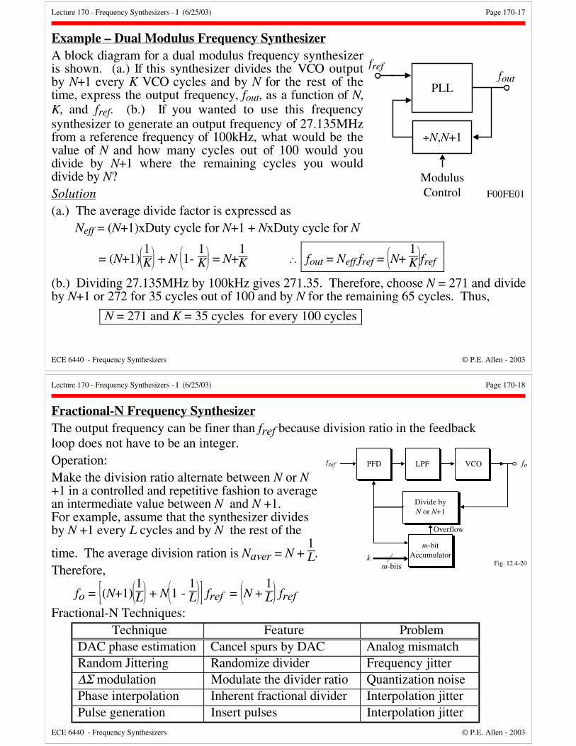
Basic Frequency Synthesizer Architecture - ContinuedFrequency Synthesizer with a Single-Modulus Prescaler:
Comments:• fo = NP·P·fref• Only the prescaler needs to run at very high speed• Since P is fixed, the value of NP is smaller causing increased channel spacing -
results in increased lock-on time and sidebands at undesirable frequenciesSolution:
PFD LPF VCO
Prescaler1/P
ProgrammableDivider 1/Np
fref fo
Fig. 12.4-17
PFD LPF VCO
Prescaler1/P
ProgrammableDivider 1/Np
fref fo
Fig. 12.4-18
1/Pfref/P
Lecture 170 - Frequency Synthesizers - I (6/25/03) Page 170-16
ECE 6440 - Frequency Synthesizers © P.E. Allen - 2003
Basic Frequency Synthesizer Architecture - ContinuedFrequency Synthesizer with a Dual-Modulus Prescaler:Operation:1.) The modulus control signal is low at thebeginning of a count cycle enabling theprescaler to divide by P +1 until the Acounter counts to zero.2.) The modulus control signal goes highenabling the prescaler to divide by P, untilthe NP counter counts down the rest of theway to zero (NP - A).3.) Thus, N = (NP – A)P +A(P+1) = NP+A
∴ fo = (NP + A)fref.4.) The modulus control is set back low, the counters are reset to their respectiveprogrammed values and the sequence is repeated.Comments:• NP > A• The value of P divided by the maximum frequency of the VCO must not exceed the
frequency capability of the NP and A counters.• P times the period of the maximum VCO frequency > the sum of the propagation delay
through the dual-modulus prescaler plus the prescaler setup or release time relative toits control signal plus the propagation delay of fref to the modulus control.
PLL
NP Counter1/NP
Dual-modulusPrescaler
1/P or 1/(P+1)
ControlLogic
A Counter
fref fo
Fig. 12.4-19
Lecture 170 - Frequency Synthesizers - I (6/25/03) Page 170-17
ECE 6440 - Frequency Synthesizers © P.E. Allen - 2003
Example – Dual Modulus Frequency SynthesizerA block diagram for a dual modulus frequency synthesizeris shown. (a.) If this synthesizer divides the VCO outputby N+1 every K VCO cycles and by N for the rest of thetime, express the output frequency, fout, as a function of N,K, and fref. (b.) If you wanted to use this frequencysynthesizer to generate an output frequency of 27.135MHzfrom a reference frequency of 100kHz, what would be thevalue of N and how many cycles out of 100 would youdivide by N+1 where the remaining cycles you woulddivide by N?Solution(a.) The average divide factor is expressed as
Neff = (N+1)xDuty cycle for N+1 + NxDuty cycle for N
= (N+1)
1
K + N
1- 1K = N+
1K ∴ fout = Neff fref =
N+ 1K fref
(b.) Dividing 27.135MHz by 100kHz gives 271.35. Therefore, choose N = 271 and divideby N+1 or 272 for 35 cycles out of 100 and by N for the remaining 65 cycles. Thus,
N = 271 and K = 35 cycles for every 100 cycles
PLL
÷N,N+1
freffout
ModulusControl F00FE01
Lecture 170 - Frequency Synthesizers - I (6/25/03) Page 170-18
ECE 6440 - Frequency Synthesizers © P.E. Allen - 2003
Fractional-N Frequency SynthesizerThe output frequency can be finer than fref because division ratio in the feedbackloop does not have to be an integer.Operation:Make the division ratio alternate between N or N+1 in a controlled and repetitive fashion to averagean intermediate value between N and N +1.For example, assume that the synthesizer dividesby N +1 every L cycles and by N the rest of the
time. The average division ration is Naver = N + 1L.
Therefore,
fo =
(N+1)
1
L + N
1 - 1L fref =
N + 1L fref
Fractional-N Techniques:Technique Feature Problem
DAC phase estimation Cancel spurs by DAC Analog mismatchRandom Jittering Randomize divider Frequency jitter∆Σ modulation Modulate the divider ratio Quantization noisePhase interpolation Inherent fractional divider Interpolation jitterPulse generation Insert pulses Interpolation jitter
PFD LPF VCO
m-bitAccumulator
Divide byN or N+1
fref fo
Fig. 12.4-20k
m-bits
Overflow

Lecture 170 - Frequency Synthesizers - I (6/25/03) Page 170-19
ECE 6440 - Frequency Synthesizers © P.E. Allen - 2003
A 1 GHz Fractional-N Frequency SynthesizerBlock diagram:
PFD/CP
a+b Da+b D
a+b D
D D
Mode Control LogicN-2 N-1 N N+1 N+2 N+3
C1 C2 D1 C3 D2
Multimodulus Prescaler÷N-2, ÷N-1, ÷N, ÷N+1, ÷N+2, ÷N+3
Controln-bits
LPF
LC VCO
Buffer Output
fref
Fig. 12.4-21
Experimental Results:
CarrierFrequency
Phase Noise,10kHz offset
Phase Noise,100kHz offset
Phase Noise,200kHz offset
Phase Noise,600kHz offset
Phase Noise,1MHz offset
972 MHz -83.1dBc/Hz -104.1dBc/Hz -110dBc/Hz -188dBc/Hz -122.4dBc/Hz916MHz -84.6dBc/Hz -104.4dBc/Hz -110.4dBc/Hz -118.2dBc/Hz -122.7dBc/Hz
Sideband spurs < -70dBc, power supply range of 2.7 to 4.5V (5.2mA at 3V), tuning range0.88-1GHz
Lecture 170 - Frequency Synthesizers - I (6/25/03) Page 170-20
ECE 6440 - Frequency Synthesizers © P.E. Allen - 2003
A Low-Noise, 1.6 GHz CMOS Frequency Synthesizer†
A CMOS PLL used to design the front-end RF function of frequency synthesizer.Block Diagram:
PFDChargePump
LoopFilter
LCVCO
Divide by 1/26
fref= 61.5MHz
fo
Fig. 12.4-23
Circuit Diagram of the LC Oscillator:Performance:• Power supply - 2.7V to 5V• Power dissipation at 3V is 90mW• Phase noise of -105dBc/Hz at 200kHz offset• Tuning range of 1.6GHz±100MHz
• 1.5mm2 in 0.6µm CMOS technology
† J.Parker and D.Ray, “A Low-Noise 1.6 GHz CMOS PLL with On-Chip Loop Filter, Proc. of 1997 Conf. on Custom Integrated Circuits, May 1997.
ISS
VDD
M1 M2
Cvar
CvarL1 L2
CAC
CAC
R
R
Fig. 12.4-24
M3
CTune
CTune
VBias
To LoopFilter

Lecture 170 - Frequency Synthesizers - I (6/25/03) Page 170-21
ECE 6440 - Frequency Synthesizers © P.E. Allen - 2003
Comparison of Recent CMOS VCO Noise Results
AuthorPower
DissipationP
Freq-uency
f0
Phase Noiseto Carrier
Ratio
OffsetFreq. (f)
EstimatedOpen Loop
QK0
Craninckx,Steyart,ISSCC95
24mW @3V 1.8 GHz -85dBc 10kHz 10 4x10-15
Rael, Abidi,ISSCC96
43mW@3V 900MHz -100dBc/Hz 100kHz 4 1.7x10⁻¹⁵
Souyer,ISSCC96
24mW@3V 4GHz -106dBc/Hz 1MHz 7 1.2x10⁻¹⁵
Thamsirianut,CICC94
7.5mW@3V 900MHz -93dBc/Hz 100kHz 1 (Class Bring osc.)
0.3x10⁻¹⁵
Weigandt,ISCAS94
10mW@3V 1GHz -85dBc/Hz 100kHz 1 (Class Aring osc.)
2.5x10⁻¹⁵
Parker, Ray,CICC97
90mW@3V 1.6GHz -105dBc/Hz 200kHz ≈7 0.6x10⁻¹⁵
Park, CICC98 17mW@3V 980MHz -109dBc/Hz 200kHz 8 0.2x10⁻¹⁵
Phase NoiseCarrier Amplitude = K0
f0
f2
1PQ
Lecture 170 - Frequency Synthesizers - I (6/25/03) Page 170-22
ECE 6440 - Frequency Synthesizers © P.E. Allen - 2003
DIVIDERS FOR FREQUENCY SYNTHESIZERSIntroductionWe have seen that in the previous material that dividers can be either fixed orprogrammable.In this section we will focus on circuits and concepts suitable for fixed, integer andfractional-N dividers.In addition, we shall consider noise-shaping techniques using delta-sigma methodsapplied to the fractional-N technique.

Lecture 170 - Frequency Synthesizers - I (6/25/03) Page 170-23
ECE 6440 - Frequency Synthesizers © P.E. Allen - 2003
Fixed DividersToggle-Flipflop based divide-by-2:
D Q
QClkvosc vdiv
Toggle-Flipflopvosc
t
t
vdiv
Fig. 4.3-11
vosc
D-Flipflop Implementation:• Proper sizing of the transistors results in
reasonable power-speed tradeoffs at GHz rates.• Device mismatches can result in phase imbalances
as large as 5°.• If the Clk input is not perfectly differential,
additional phase unbalances can occur. D
Q
Q
Clk
+
-
+
-
VDD
RL RL
M1 M2
M3
M4 M5
M6
Fig. 4.3-12
Lecture 170 - Frequency Synthesizers - I (6/25/03) Page 170-24
ECE 6440 - Frequency Synthesizers © P.E. Allen - 2003
Dual Modulus DividersEvolution of a divide-by-2/3 from a divide-by-3 circuit:
D Q
ClkFF1
D
QClkFF2
Clk
Q1
Q2
Fig. 4.3-13
Clk
t
t
Q1
t
t
Q2
G
G
G1
N=3
Divide-by-2/3 circuit (MC=1 → ÷2, MC=0 → ÷3):
D Q
ClkFF1
D
QClkFF2
Clk
Q1
Q2
Fig. 4.3-14
Clk
t
t
Q1
t
t
Q2
G
G
G1
MC
N=2

Lecture 170 - Frequency Synthesizers - I (6/25/03) Page 170-25
ECE 6440 - Frequency Synthesizers © P.E. Allen - 2003
Dual Modulus Dividers - ContinuedState diagram of the divide by 2/3 circuit:
"1"Q1Q2:00
MC=0
Q1Q2:01
Q1Q2:01
Q1Q2:11"1"
"0"
"X"
"X"2/3
decision point Fig4.3-135
Lecture 170 - Frequency Synthesizers - I (6/25/03) Page 170-26
ECE 6440 - Frequency Synthesizers © P.E. Allen - 2003
Speed of the Dual Modulus DividerThe divide-by-3 circuits are generally much slower than their divide-by-two counterparts.Consider the implementation of part of the previous divide-by-2/3 circuit.
D
Q2
Q2
Clk
+
-
+
-
VDD
RL RL
M1 M2
M3
M4 M5
M6
Fig. 4.3-15
RL RL
M1 M2
M3
VDDG1 FF2
On the clock edge where Q2 must change, sufficient time must be allowed for the delayof the AND gate, G1, and the input stage of FF2 before the next clock transition.
It is seen that the delay for ÷3 circuit is nearly twice that of the ÷2 circuit.

Lecture 170 - Frequency Synthesizers - I (6/25/03) Page 170-27
ECE 6440 - Frequency Synthesizers © P.E. Allen - 2003
Programmable DividersA divider can be achieved by using aprogrammable counter.
For a given speed requirement, a programmabledivider is less power optimized because thecritical path is dependent on the loaded value.A complete divider consisting of a fixed divider cascaded with a programmable divider.
Fixed CounterN1
Programmable CounterN2
Max. count = N2(max)
fintermediatefo fdivide
Power is high, powercan be optimized
Power is low, powercannot be optimized Fig. 4.3-17
Resolution (Complete divider)= Resolution (programmable divider) x Division ratio (fixed divider)
D
Clk
ProgrammableCounter, N2
Maximum count = N2
Preload Input(= division ratio M)
Counter Output(= fdivide)
Preload Enable
Clock (= fo)
Fig. 4.3-16
Lecture 170 - Frequency Synthesizers - I (6/25/03) Page 170-28
ECE 6440 - Frequency Synthesizers © P.E. Allen - 2003
Waveforms of Various Complete DividersN1 = 3 and N2 = 4:
fo
fintermediate
fdividefdivide = fo/12
Fig. 4.3-18
3 3 3 3
12
N1 = 3 and N2 = 3:
fo
fintermediate
fdividefdivide = fo/9
Fig. 4.3-19
3 3 3
9

Lecture 170 - Frequency Synthesizers - I (6/25/03) Page 170-29
ECE 6440 - Frequency Synthesizers © P.E. Allen - 2003
Waveforms of Various Complete Dividers – ContinuedN1 = 3/4 (N1 = 4 for one N2 cycle) and N2 = 3:
fo
fintermediate
fdividefdivide = fo/10
Fig. 4.3-20
4 3 3
10
N1 = 3/4 (N1 = 4 for two N2 cycles) and N2 = 3:
fo
fintermediate
fdividefdivide = fo/11
Fig. 4.3-20
34 4
11
Lecture 170 - Frequency Synthesizers - I (6/25/03) Page 170-30
ECE 6440 - Frequency Synthesizers © P.E. Allen - 2003
Multi-Modulus Dividers÷4/÷5 dual modulus counter example:
D Q
Clk
D Q
Clk
D Q
Clk
d2
Q3
MC
fps
Q2Q1
fo
d1d0 f÷4,÷5
Fig. 4.3-22
State Diagram:Note that there are two possible state paths A and Beach consisting of two sequences, a ÷4 sequence anda ÷5 sequence.For path A, the ÷4 sequence is from 000, 001,011,010, 000 and the ÷5 sequence is from 000, 001, 011,010, 100, 000.For path B, the ÷4 sequence is from 000, 001, 011,110, 000 and the ÷5 sequence is from 000, 001, 011,110, 100, 000.
000
001010100
011110
X0
0 X
1
1
X
0
4/5 decision point
Path A
Path BPath B
Fig. 4.3-23

Lecture 170 - Frequency Synthesizers - I (6/25/03) Page 170-31
ECE 6440 - Frequency Synthesizers © P.E. Allen - 2003
NOISE SHAPING TECHNIQUESDelta-Sigma Shaping Techniques
Delta-sigma modulators can be used along with mulitmodulus dividers to achieve noiseshaping of phase noise.
The objective of the delta-sigma modulator is to remove the noise due to thefluctuation of the mulitmodulus dividers.
The following slides review this technique as applied to frequency synthesizers.Analog implementation of a first-order delta-sigma modulator:
Integrator
1-bit quantizer
1-bit DAC D
+
-
x(t) y(nT)
Fig. 4.3-24
Lecture 170 - Frequency Synthesizers - I (6/25/03) Page 170-32
ECE 6440 - Frequency Synthesizers © P.E. Allen - 2003
Digital Implementation of the Delta-Sigma Modulator
Input, k
m-bits
m-bits
m-bits
D
1-bit Output
Residue,R
Clock
+-z-1
z-12m
Y(z)
2m
0
01
1-bit quantizerF(z) + +
+-
A(z)Y(z)A(z)
Q(z)
++
Fig. 4.3-25
The discrete first-order delta-sigma modulator can be implemented with an m-bitaccumulator. The m-bit accumulator has m input bits, a single output bit (carry-bit orMSB), and m-residue bits.Operation:
On every cycle of the reference clock, the residue output R of the accumulator isassigned the value R+k after one cycle if an overflow does not occur or the value R+k-2m ifthe accumulator produces a carry-bit signal.
Therefore, the accumulator overflow is equivalent to the comparator decision. Thedata stored in the accumulator is essentially the integral of the error between the desiredfrequency data k and the actual frequency control input.

Lecture 170 - Frequency Synthesizers - I (6/25/03) Page 170-33
ECE 6440 - Frequency Synthesizers © P.E. Allen - 2003
High-Order Delta-Sigma Modulatorsz-transform of a first-order delta-sigma modulator:
1-z-11
z-1
InputF(z)
Q(z)
Y(z)
-Q(z)
+
+
+ +
-
-
Fig. 4.3-26
n-th order delta-sigma modulator:
y(n)
First-Order Sigma-Delta Modulator
f(n) y1(n)
First-Order Sigma-Delta Modulator
-q1(n) y2(n)
First-Order Sigma-Delta Modulator
-q2(n) y3(n)
First-Order Sigma-Delta Modulator
-qN(n) yN+1(n)
BitManipulation
Circuitry
Fig. 4.3-27
Lecture 170 - Frequency Synthesizers - I (6/25/03) Page 170-34
ECE 6440 - Frequency Synthesizers © P.E. Allen - 2003
Use of a Modulator for Divider ControlConsider the second-order delta-sigma modulator implemented with m-bit accumulators:
Input, km-bits
m-bits
m-bits
D
Residue,R
m-bits
m-bits
m-bits
D
Residue,R
D
+1 -1+1Adder
Bit Manipulation Circuitry
y(n)
Fig. 4.3-28

Lecture 170 - Frequency Synthesizers - I (6/25/03) Page 170-35
ECE 6440 - Frequency Synthesizers © P.E. Allen - 2003
Use of a Modulator for Divider Control – Continuedz-tranform model for the previous second-order delta-sigma modulator:
1-z-11
z-1
InputF(z)
Q1(z)
Y1(z)
-Q1(z)
+
+
+ +
-
-
1-z-11
z-1
Q2(z)
Y(z)
+ +
+ +
-
-
Fig. 4.3-29
z-1
Y2(z)
From the above diagram, we can write,
Y1(z) = F(z) + (1-z-1)Q1(z) and Y2(z) = -Q1(z)(1-z-1) + Q2(z)(1-z-1)2
can be combined to give,
Y (z) = F(z) + + Q2(z)(1-z-1)2
Generalizing to the n-th order gives,
Y (z) = F(z) + + Qn(z)(1-z-1)n
Lecture 170 - Frequency Synthesizers - I (6/25/03) Page 170-36
ECE 6440 - Frequency Synthesizers © P.E. Allen - 2003
Use of a Modulator for Divider Control – ContinuedThe effective divide ratio of a fractional divider implemented with an n-th order delta-sigma modulator can be written as,
Neff = N(z) + Y(z) = N(z) + F(z) + Qn(z)(1-z-1)n
whereN(z) = integer part of the divide ratioF(z) = fractional part of the divide ratioQ(z) = quantization noise occurring at the n-th delta-sigma modulator
If the PLL is in lock, then
fo = Neff ·fref = [N(z) + F(z)] fref + (1-z-1)nQn(z) fref
where the first term is the desired frequency and the second term represent the frequencyfluctuation resulting from the quantization noise in the fractional modulator.

Lecture 170 - Frequency Synthesizers - I (6/25/03) Page 170-37
ECE 6440 - Frequency Synthesizers © P.E. Allen - 2003
Use of a Modulator for Divider Control – ContinuedAssume that the quantization noise is a random quantity in the interval {-0.5∆, +0.5∆}with equal probability. If the quantizer is 1-bit, then ∆ which is the quantization step sizeis 1.
The noise power or variance, σ 2e , can be found as
σ 2e = E(e) = 1∆ ⌡⌠
-0.5∆
0.5∆
e2de = ∆ 212
The spectrum of the quantization noise iswhere N(f) is given as,
N(f) = ∆ 2
12fref
where fref is the sampling frequency which is equal to the comparison frequency of thePFD.
N(f)
f-fref fref Fig. 4.3-30
Lecture 170 - Frequency Synthesizers - I (6/25/03) Page 170-38
ECE 6440 - Frequency Synthesizers © P.E. Allen - 2003
Use of a Modulator for Divider Control – ContinuedDefine ∆f(z) as the frequency noise of fluctuation of the output frequency fo(z). Thepower spectral density, S∆f(z), can be calculated from the second term of the previousexpression for fo(z).
∴ S∆f(z) = |(1-z-1)nfref |2 ∆ 2
12fref = |(1-z-1)nfref |2
112fref
= |(1-z-1)|2n fref12
Because phase is related to frequency through integration, the phase noise, θn(t), is
θn(t) = 2π⌡⌠∆f(t)dt
Using a simple rectangular integration in the z-domain yields,
Θn(z) = 2π ∆f(z)fref(1-z-1)
The power spectral density of the phase noise, SΘn(z), can be written as,
SΘn(z) = |Θn(z)|2 S∆f(z) = (2π)2
fref2|1-z-1|2 S∆f(z) =
(2π)2|1-z-1|2(n-1)
12 fref rads2/Hz
Assuming SΘn(f) is a two-sided power spectral density function gives L(f) = SΘn(f)
∴ L(f) = (2π)2
12 fref
2sin
πf
fref
2(n-1) rads2/Hz
where z-1 has been replaced with e-j2πf/fref and n is the order of the modulator.

Lecture 170 - Frequency Synthesizers - I (6/25/03) Page 170-39
ECE 6440 - Frequency Synthesizers © P.E. Allen - 2003
Use of a Modulator for Divider Control – ContinuedPredicted phase noise of higher-order modulators (fsample = 12.8 MHz):
Lecture 170 - Frequency Synthesizers - I (6/25/03) Page 170-40
ECE 6440 - Frequency Synthesizers © P.E. Allen - 2003
Use of a Modulator for Divider Control – ContinuedResults:
If a modulator has an accumulator input data k consisting of m bits, then the oscillatoroutput frequency, fo, can be given as,
fo =
N + k
2m fref
The uncertainty of this frequency will be reduced by the use of the sigma-delta modulator.
Summary:• The delta-sigma modulator attenuates phase noise from the factional controller to
negligible levels close to the center frequency.• Further from the center frequency, the phase noise increase rapidly and must be filtered
out prior to tuning the input of the VCO.• The loop filter in the PLL is used to filter the noise away from the center frequency.• When a higher-order, delta-sigma modulator is used for a fractional-N controller, the
PLL needs more poles in the loop filter to suppress the quantization noise at highfrequencies.

Lecture 170 - Frequency Synthesizers - I (6/25/03) Page 170-41
ECE 6440 - Frequency Synthesizers © P.E. Allen - 2003
SUMMARY• Examine the applications of PLLs
1.) Demodulation and modulation2.) Signal conditioning3.) Frequency synthesis4.) Clock and data recovery5.) Frequency translation
• Integrated Circuit Frequency Synthesizers – Architectures and Techniques- Fractional N- Dividers/prescalers- Noise shaping techniques