Dissertation Design and Simulate Radio Frequency (RF) CMOS ...
46
Dissertation Design and Simulate Radio Frequency (RF) CMOS Mixer Circuit by Muhammad Syazwan bin Muhammad Adib (5751) Dissertation submitted in partial fulfilment of the requirements for the Bachelor of Engineering (Hons) (Electrical & Electronics Engineering) June 2008 Universiti Teknologi PETRONAS Bandar Seri Iskandar 31750 Tronoh Perak Dam! Ridzuan
Transcript of Dissertation Design and Simulate Radio Frequency (RF) CMOS ...

Dissertation
Design and Simulate Radio Frequency (RF) CMOS Mixer Circuit
by
Muhammad Syazwan bin Muhammad Adib (5751)
Dissertation submitted in partial fulfilment of
the requirements for the
Bachelor of Engineering (Hons)
(Electrical & Electronics Engineering)
June 2008
Universiti Teknologi PETRONAS
Bandar Seri Iskandar
31750 Tronoh
Perak Dam! Ridzuan

CERTIFICATION OF APPROVAL
Design and Simulate Radio Frequency (RF) CMOS Mixer Circuit
Approved by,
by
Muhammad Syazwan bin Muhammad Adib
A project dissertation submitted to the
Electrical & Electronics Engineering Programme
Universiti Teknologi PETRONAS
in partial fulfilment of the requirement for the
BACHELOR OF ENGINEERING (Hons)
(ELECTRICAL & ELECTRONICS ENGINEERING)
(A.P. Dr Mohammad b A wan)
UNIVERSITI TEKNOLOGI PETRONAS
TRONOH, PERAK
JUNE2008

CERTIFICATION OF ORIGINALITY
This is to certifY that I am responsible for the work submitted in this project, that the
original work is my own except as specified in the references and
acknowledgements, and that the original work contained herein have not been
undertaken or done by unspecified sources or persons.
MUHAMMADSY

Acknowledgment
"I would like to take this opportunity to express my heartfelt gratitude to those who
had contributed in making my final year project (FYP) a success; whether directly or
indirectly. To A.P. Dr Mohammad b A wan; your continuous support, good guidance
and useful advices shall always be appreciated. My sincere gratitude also goes to
my parent and my colleagues, for their continuous support and useful advices which
I shall forever remember. Thank You."
[Muhammad Syazwan b Muhammad Adib, Electrical Department- Jan 2008]

ABSTRACT
Radio frequency design has been one of the principal research areas in the· recent past.
Much of work has been done in integrating data with wireless communication. Since
a decade ago, the frequencies for such communication have been in free bands
available in the low frequency spectrum like 900 MHz and lower. With rapid
improvement in the technology of microelectronic nowadays, these frequency
spectrums are improved to be within the range of ultra band frequencies of GHz.
These emergences of several RF Wireless Communication standards of
communication have demanded availability of low cost analogue blocks for use in
transceiver. Despite rigorous research undergoing, it has been difficult to meet the
design specification by low cost technologies like CMOS. In this project, the
presented mixer down converts Radio Frequency (RF) of 1.8 GHz to 200 MHz
which typifies specifications for a GSM 1800 receiver with Voltage Conversion Gain
(VCG) of 7.703 dB, IIP3 of 10.916 dBm and Noise Figure (NF) of 11.094 dB with
current utilization of 6 rnA. This hi.gh conversion gain and low noise figure mixer is
achieved by utilizing Differential Gilbert Mixer Cell. The mixer was simulated in
analogue environment of Spectra Cadence Schematic.

TABLE OF CONTENT
ABSTRACT .............................................................................................. ! TABLE OF CONTENT ......................................................................... II LIST OF FIGURES .............................................................................. IV LIST OF TABLES ................................................................................. V ABBREVIATIONS AND NOMENCLATURES ............................... VI CHAPTER 1: INTRODUCTION .......................................................... l
1.0 Background of Study .................................................................................... !
1.1 Problem Statement ........................................................................................ I
1.2 Objectives and Scope of Study ..................................................................... !
CHAPTER 2: LITERATURE REVIEW ............................................. 3 2.0 Mixer Theory ............................................................................................... .3
2.1
2.1.1
Preliminary Aspect Of The Mixer Design ................................................... .4
CMOS Technology .............................................................................. .4
2.1.2 Competing Technology ........................................................................ 5
2.1.2.1 Gallium Arsenide Technology (GaAs) ............................................. 6
2.1.2.2 Bipolar Complementary MOS Technology (BiCMOS) ................... 6
2.2 Advantages and Disadvantages ofCMOS .................................................... 7
2.2.1 Advantages ofCMOS ........................................................................... 7
2.2.2 Disadvantages of CMOS ...................................................................... 8
2.3 Passive Device Used in CMOS Technology ................................................ 8
2.3 .I Resistors ................................................................................................ 8
2.4 Type of Noises Available ............................................................................. 9
2.4.1 DSB and SSB ........................................................................................ 9
2.4.2 LO Leakage ........................................................................................ 10
2.5 Mixer Performances .................................................................................... ! 0
2.5.1
2.5.2
2.5.2.1
2.5.2.2
2.5.3
Voltage Conversion Gain ................................................................... ! 0
Linearity .............................................................................................. 11
1 dB Gain Compression Point ........................................................ .11
3'd Order Intercept Point (IIP3) ...................................................... .11
Noise Figure ........................................................................................ l2
11

2.6
2.6.1
Mixer Topologies ........................................................................................ 12
2.6.2
2.6.3
2.6.4
2.6.5
2.7
2.7.1
2.7.2
2.7.3
Single-Balanced Design ...................................................................... 13
Gilbert Cell with Differential Inputs ................................................... 13
Gilbert Cell with Single-Ended Inputs .............................................. .14
Micromizer ......................................................................................... 15
Common Gate-Common Source (CG-CS) Mixer .............................. 15
Mixer Design Characteristic ....................................................................... 16
Single Balanced vs Double Balanced Mixer ...................................... 16
MOS Behavior .................................................................................... 18
Switching Stage .................................................................................. 18
CHAPTER 3: METHODOLOGY ...................................................... 19 3.0 Introduction ................................................................................................. 19
3 .I Design Approach ........................................................................................ 20
3.1.1 RF Stage .............................................................................................. 21
3.1.2 LO Stage ............................................................................................. 21
3.1.3 Current Sinks ...................................................................................... 22
3.2 Circuit Schematic ........................................................................................ 23
CHAPTER 4: RESULT AND DISCUSSION .................................... 24 4.0 Schematic Simulation ................................................................................. 24
4.1 Transient Analysis ...................................................................................... 25
4.2 Voltage Conversion Gain ........................................................................... 27
4.3 The !dB Compression Point... .................................................................... 28
4.4 The Input 3'd Order Intercept Point (IIP3) .................................................. 29
4.5 PNOISE Analysis ....................................................................................... 29
CHAPTER 5: CONCLUSION AND RECOMMENDATION ......... 31 5.0 Conclusion and Recommendation .............................................................. 31
5.1 Future Work ................................................................................................ 32
REFERENCES ...................................................................................... 33 APPENDICES ....................................................................................... 34
111

LIST OF FIGURES
Figure 1: Multiplication of Two Different Frequency Terms ................................... .4
Figure 2: Cross Section of an NMOS ........................................................................ 5
Figure 3: Cross Sectional View ofGaAs MESFET ................................................... 6
Figure 4: Cross Sectional View of Devices in BiCMOS Process .............................. ?
Figure 5: Accumulation ofRF and Image Noise into The IF Band ........................... 9
Figure 6: Output Frequency Spectrum of Double Balanced Mixer. ....................... .lO
Figure 7: ldB Compression Point ............................................................................ ll
Figure 8: Frequency Spectrum of Two Tones Test of Mixer ................................. .12
Figure 9: Schematic of a Single-Balanced Design Mixer. ....................................... 13
Figure 10: Schematic of a Gilbert Cell with Differential Inputs ............................ l4
Figure 11: Schematic of a Gilbert Cell with Single-Ended Inputs ......................... 14
Figure 12: Schematic of a Micromizer. .................................................................. 15
Figure 13: Schematic of a Common-Gate Common-Source Mixer. ...................... 16
Figure 14: Schematic of Single Balance Mixer ..................................................... 17
Figure 15: Schematic of Double Balance Mixer .................................................... 17
Figure 16: I d' vs Vd, Plot showing the Different Regions of Operation ............... 18
Figure 17: Flow Chart ofProject. ........................................................................... l9
Figure 18: Two Current Sinks Circuit .................................................................... 22
Figure 19: Finalized Gilbert Cell Mixer. ................................................................ 23
Figure 20: The Gilbert Mixer Schematic View ...................................................... 24
Figure 21: The Oscillator Circuit for RF and LO Signal ....................................... 25
Figure 22: The Radio Frequency (RF) Signal located at 1.8 GHz ......................... 25
Figure 23: The Local Oscillator (LO) Signal located at 1.6 GHz .......................... 26
Figure 24: The Intermediate Frequency (IF) Signal located at 200 MHz .............. 26
Figure 25: Voltage Conversion Gain in PSS Simulation for 6 mA ........................ 27
Figure 26: !dB Compression Point in PSS Simulation for 6 mA ........................... 28
Figure 27: Noise Figure in PNOISE analysis for 6 mA .......................................... 30
IV

LIST OF TABLES
Table 1: Model parameters ofNMOS .................................................................... 20
Table 2: Values from the Calculation for Schematic ............................................. 23
Table 3: Voltage Conversion Gain (dB) for Different Currents ............................. 27
Table 4: ldB Compression Point (dBm) for Different Currents ............................ 28
Table 5: 3'd Order Intercept Point (IIP3) for Different Currents ............................ 29
Table 6: Noise Figure (dB) for Different Currents ................................................. 30
v

BICMOS
CMOS
CG-CS
dB
dBm
DC
DRC
DSB
GaAs
gm
IC
IF
IIP3
LNA
LO
LVS
MOS
MOSFET
NF
R
RF
RFICs
PSS
SNR
SSB
VCG
WiFi
ABBREVIATIONS AND NOMENCLATURES
Bipolar Complimentary Metal Oxide Semiconductor
Complimentary Metal Oxide Semiconductor
Common Gate-Common Source
Decibels
Decibels with respect to lm W
Direct Current
Design Check Rule
Double Side Band
Gallium Arsenide
Gate Transconductance of a MOSFET
Integrated Circuit
Intermediate Frequency
Input 3 rct Order Intercept Point
Low Noise Amplifier
Local Oscillator
Layout versus Schematic
Metal Oxide Semiconductor
Metal Oxide Semiconductor Field Effect Transistor
Noise Figure
Resistance
Radio Frequency
Radio Frequency ICs
Periodic Steady State
Signal to Noise Ratio
Single Side Band
Voltage Conversion Gain
Wireless Fidelity
VI

CHAPTER!
INTRODUCTION
1.0 Background of Study
The purpose of a CMOS mixer is to convert a base band or intermediate
frequency to the higher RF frequency (up-conversion mixer) or to translate an RF
frequency to a lower frequency base-band or Intermediate Frequency (IF) (down
conversion mixer) by multiplying the input signal with Local Oscillator (LO) signal.
This report describes a down converter CMOS mixer that converts RF of 1.8 GHz to
200MHz.
1.1 Problem Statement
The frequency translation process in a CMOS mixer will generate some
unwanted signal or noises to degrade the Signal-to-Noise ratio (SNR). Linearity of a
mixer also is an essential factor in designing a good high gain mixer and the linearity
of the mixer effects. There are some tradeoffs with having high linearity and gain,
the power consumption and noise of the circuit will also increase as well [ 1].
1.2 Objectives and Scope of Study
The objectives ofthe study are:
• To come up with a good design of a CMOS mixer circuit with high linearity
and has the quality to improve the output to input gain as well as the SNR
ratio.
• To simulate the complete circuit of a CMOS mixer using SPECTRE and
verify its performances.
• To do some improvisations on the design parameters of the simulated mixer
circuit wherever applicable.
I

The scope of study is to present the designed-CMOS mixer performance on
Gain, !dB Compression Gain, 3'd Order Intercept Point, Noise Figure (NF) and
linearity by setting it up to the set design specifications.
The following specifications are used for guideline in designing a CMOS
mixer circuit [I] :
Total Current< 20mA
Vaa = 3.3V
Power Consumption < 66m W
IIP3 > 20dBm
Gain between 0 to SdB
Noise Figure< 18dB
RF signal = 1.8 GHz
LO signal = 1.6 GHz
The figures for the specification are used based on the latest design of a CMOS
mixer circuit for a cable tuner utilizing 0.18 fllibrary technology.
2.

2.0 Mixer Theory
CHAPTER2
LITERATURE REVIEW
Mixer; or frequency converters are also sometimes called multipliers and in
the early days of super heterodyne receivers they were often called "detectors".
Whatever name it is known by, the requirement is that the mixer has the ability to:
• Convert the desired signal from the received frequency to the receiver's first
IF frequency.
• Convert the signal with minimum distortion and/or additive noise
• Convert the signal with minimum loss
• Convert the signal with good frequency accuracy
Mixers are used for frequency translation; they convert the Radio Frequency
(RF) to Intermediate Frequency (IF) by multiplying it with the Local Oscillator (LO)
signal applied to the mixers. The operation is as shown in Figure 1. The mixing
outcome produces two signal located at Ww + wRF and Ww- wRF frequency. One
signal is the wanted signal and the other is the unwanted based on what type the
mixer is configured whether an up converting or a down converting mixer
respectively [1]. The method of operation can be defined by equation (1).
3

Mag ~-------------,--------------,
Subtractive term Ww- wRF
' '
0 ' ' ,/ ',
' '
' ' ' '
WRF \
Freq
Additive term Ww - wRF
Figure 1: Multiplication of Two Different Frequency Terms
I V,u,(t) = -(cos(w1 - w2)1 + cos(w1 + w,)t)
2
2.1 Preliminary Aspect of The Mixer Design
(1)
There are a few aspects that need to be understood in order to design a good
CMOS mixer circuit. There are as follow:
2.1.1 CMOS Technology
CMOS Is also known as complementary-symmetry metal-oxide
semiconductor which the term "complementary-symmetry" is referring to the fact
that the digital design style of CMOS uses complementary and symmetrical pairs of
p-type and n-type MOSFETs for logic functions.
A metal-oxide-semiconductor field-effect transistor (MOSFET) is based on
the modulation of charge concentration caused by aMOS capacitance [2]. MOSFET
have two terminals (source and drain) where each is connected to separate highly
doped regions. These regions can be either p-type or n-type, but with condition that
they must both be of the same type. These two regions must be separated with a
4

highly doped region of the same type which is called as the 'body' as shown in
Figure 2. The 'gate' which is the active region of the MOS constitutes a MOS
capacitance with a third electrode. This region is located above the 'body' and
usually insulated with an oxide to separate it from the other regions.
Source Gate Drain
L p
Body
Figure 2: Cross Section of an NMOS
For an N-channel or n-MOSFET as in Figure 2, the source and the drain are
from the 'n+' regions whereas the body is a 'p' region. As method of operation,
when a positive voltage is supplied to the gate-source; by depleting the region of hole
thus an N -channel will be created at the surface of the P region. This channel
extends between the source and the drain. Current will only be conducted through
this channel when the gate potential is high enough to attract electrons from the
source into the channel. In contrary, when negative voltage is supplied to the gate
source, this channel disappears thus no current can flow from the source to the drain.
2.1.2 Competing Technology
The market interest is evolving from high cost technologies like GaAs
(Gallium Arsenide) that provides active and passive devices able to work at radio
frequency, but characterized by a low scale of integration; to a low cost standard
technology like CMOS [2].
5

2.1.2.1 Gallium Arsenide Technology (GaAs)
GaAs gas can be found in high frequencies IC mainly due to its properties of
high electron mobility (approximately 5 to 10 times more than Silicon) and high peak
velocity. Thus for the same input voltages GaAs devices have higher output currents,
and thus higher gm than the corresponding silicon devices [2]. One characteristic that
GaAs has is it enables faster charging and discharging of both load and parasitic
capacitance which results in an increase in speed of operation. In addition, the
substrate has higher resistivity (almost five times larger than silicon) which reduces
the cross talk between devices.
Sfl!J
' --. ....
Anod~ Catodc Schottky-barrier
metal \
MESI·ET
S{m~cc (S) Gate {G) Drain I: D)
II'
L t '----'-----l/ Ciumnd
Scm1-ins.ularing C·aAs suhstrahl
Figure 3: Cross Sectional View ofGaAs MESFET
MESFET is a good example of device which utilizes this type of technology
as in Figure 3. It operations is very similar to the silicon JFET but only for n
MOSFET. This technology cannot be implemented for p-mosfet as holes have
relatively low drift mobility to be used in GaAs. In fact, this is the advantage of using
GaAs technology as it lacks of complementary transistors. Another important feature
that allows GaAs integrated circuits to have perfect performance in the GHz bands is
the availability of high quality passive components [2].
2.1.2.2 Bipolar Complementary MOS Technology (BiCMOS)
This technology as laid in Figure 4 combines the abilities of CMOS like high
scale integration, low power consumption, high noise immunity with plus points of
bipolar technologies like high speed and high drive capabilities [2]. Definitely, this
6

technology is better than GaAs in term of cost estimation, but still costly relatively to
the CMOS technology as it requires additional masks. Similarly to GaAs, the
resistivity of the silicon substrate used in this technology is higher than CMOS
technology. This is beneficial as it reduces the cross talk between devices.
N-MOS P-MOS 1\PN
S G D S (j D C E ll
10 I-' I n--cpi -'---"- i:J ( n-wcll) p- well (n-well) p-
.p+ ' n+buried H n+buried "'"'--'
p- substmt-c
D Ll D D El D . .
p- subsume p+ n-~ri n+ buried n+sink.:r Oxide
Figure 4: Cross Sectional View of Devices in BiCMOS Process
2.2 Advantages and Disadvantages of CMOS
As with the other available technologies, there are a few advantages and
disadvantages of CMOS and it will be described in the next sub-section as follow:
2.2.1 Advantages of CMOS
The single major advantage of CMOS lies in very cheap and well-designed
fabrication processes [2]. Undeniably, cost is a major concern in the chip-related
industry, which CMOS is by far, the most economical in comparison to the other
technologies. It is to be estimated that GaAs is at least 200 times costlier to MOS
whereas Bipolar is 50 times. Furthermore, the fabrication of the CMOS has wide
popularity due to its extensive digital design. Lately, with decrease in the channel
length, the maximum usable frequency ofMOS has also gone higher up to GHz [2].
7
2.2.2 Disadvantages of CMOS
MOS to be known not be suited for high frequency operation. MOS has a
lower unity gain frequency as compared to the other competing technology. Besides,
CMOS tends to be an undefined model at high frequency [2]. This is due to MOS has
unpredictable operations at high frequency with low frequency models failed as well
to predict its operations. Therefore, there surely is a difficulty when it comes to
design using MOS as design tools when it fails to predict its exact operation. The
noise contributed from MOS as well need to be studied properly as other
technologies do not suffer from inconsistency of behaviour unlike CMOS.
2.3 Passive Device Used in CMOS Technology
Other than MOSFET which is an active device, there is as well passive
device used in the CMOS technology such as resistor.
2.3.1 Resistors
There are several options available for resistor in MOS process include poly,
source-drain diffusions, well, MOS transistor, metal interconnect and many more.
Poly has more resistivity than metal layers, tolerance is often poor and the
temperature coefficient may go high but in contrary it has the advantage of
reasonable low parasitic capacitance per unit area and low voltage coefficients [2].
Source drain is very similar to poly in term of characteristic, but with larger parasitic
capacitance and lower temperature coefficient. Meanwhile, well provides higher
resistance of the order 1-10 k0. but it has large parasitic capacitance, large
temperature and voltage coefficients [2].
MOS transistors can be used as a resistor with suitable gate to source voltage.
Incremental resistance of a long channel MOS in triode region is as in equation (2).
(2)
8

2.4 Type of Noises Available
Undeniably, noise contributes a big motivation in almost all circuit design.
But in wireless front -end design, its importance is overwhelmed. In electronics, noise
is usually referred as unwanted signal that contains no information. There are many
potential sources of noise which are external noise; which can be minimized using
any shielding method while the other one is internal noise (fundamental noise). The
latter type cannot be cancelled, but can only be minimized through better design.
There a few types of fundamental noises in electronic systems; Thermal Noise, Shot
Noise, Flicker Noise, Popcorn Noise and many more. However, these noises are not
as significant as DSB and SSB noise figure and noises due to LO leakage.
2.4.1 DSB and SSB
When two signals are multiplied, two different frequencies terms will show
up which are the additive term and the subtractive term. The output frequency
spectrum also consists of two terms if the LO frequency is fixed. The IF term
consists of two terms; one is w w - w RF which is the desired frequency term and the
other is w IM - w w . If the image term is considered, the amount of noise in the IF
frequency spectrum will be doubled. If the noise figure is considered neglecting the
image noise, it is called as double side band (DSB) noise figure. If the image noise is
considered then it is called as single side band (SSB). However, SSB is 3dB higher
than DSB noise as in Figure 5.
Mag
t t t Freq
Ww -WRF WIF
+wiM -ww
Figure 5: Accumulation ofRF and Image Noise into The IF Band
9

2.4.2 LO Leakage
If a single balanced mixer is used, the LO signal appears at the IF output due
to the bias current as in Figure 6, and the LO leakage signal makes the design of the
IF filter more difficult because the LO leakage signal is close to IF frequency. Most
of the LO leakage problems are caused by transistor mismatches [2]. The LO leakage
problem is solved by using a double balanced mixer so that the DC bias current term
at the output is cancelled. Hence, the LO signal does not appear at the IF output
anymore.
Mag
Freq
Ww+WRF 3wLO-wRF 3wLo+WRF SwLo w 5 + - RF WLO WRF
Figure 6: Output Frequency Spectrum of Double Balanced Mixer
2.5 Mixer Performances
. There are several criteria that can be observed as measurement to the
performance level of the CMOS Mixer. These include the Voltage Conversion Gain,
Linearity as well as the Noise Figure.
2.5.1 Voltage Conversion Gain
Voltage Conversion Gain of a mixer is defined as the Root Mean Square (rms)
voltage of the signal at the IF frequency divided by the rms voltage of the signal at
the RF frequency [1]. The two basic types are conversion voltage gain and
conversion power gain. If all switching MOS are perfect switches, therefore the
conversion voltage gain can be approximated as following in equation (3).
G -2 R v--gm. out (3) 7r
10

Hence the conversion power gain is as in equation ( 4).
( )
2 2 R,,
Gp = -gm.Rout -7r Rout
(4)
2.5.2 Linearity
Linearity describes the region of operation where the output signal varies
proportionally to the input signal. There are several ways of measuring linearity
performance of a mixer such as !dB gain compression point and 3'd order intercept
point (IIP3) [3].
2.5.2.1 ldB Gain Compression Point
The I dB gain compression point is defined as the input power level in dBm at
which the overall gain of amplifier is reduced by ldBm from its maximum value
where it would have been if it were an ideally linear device [3] as in Figure 7.
ldB 20log Aout
20!ogA,,
Figure 7: 1 dB Compression Point
2.5.2.2 3'd Order Intercept Point (IIP3)
It is a theoretical point at which the fundamental and third order response
intercepts. This point is found when two signals that are very close in frequency are
applied to the mixer as shown in Figure 8. Suppose the input power level at J; is the
same as at J; . The IIP3 is defined as the intercept point of the extrapolated line of
11

output power at frequency ho- (2 1,- /;)versus extrapolated line of the linear output
ho- J; [4]. !dB compression point is about 9.66dBm below the intercept point of
IIP3, thus equation ( 5) states
IIP3 = ldB compression point (in dBm) + 9.66dBm (5)
--, / ' - ' - ' / ' - ' / '
' ' Mag
;' "~ - - ' ' ' ' w if I - w,o ,/ ,/ ·.
' ' ' ' \ .:/ : /? 2wrf- w1o •
Freq.
Figure 8: Frequency Spectrum of Two Tones Test of Mixer
2.5.3 Noise Figure
Noise Figure (NF) calculates how much the SNR of a signal degrades
'because of the added noise as it passes through the mixer. The NF of the mixer is
defined as the ratio of total SNR of the RF signal to the total SNR ofiF signal [3] as
in equation (6).
NF(dB) = lOlog( SNR;. ) SNRont
2.6 Mixer Topologies
(6)
Passive mixers have higher linearity and better frequency response but they
do not have any gain thus are not widely used in RF systems. On the other hand,
active mixers have gain hence reducing noise contributed by the succeeding stages
[ 4]. There are five types of active mixer topologies available as follow:
12

2.6.1 Single-Balanced Design
This design is the simplest approach that can be implemented in most
semiconductor processes. It offers a desired single-ended RF input for ease of
application as it does not require a balun transformer at the input [ 4]. It also has
moderate gain and low noise figure. This topology is as presented in Figure 9 .
• -· -·-· -1 ~ i;11~: • I
l . -· -· _j~ ,,:,o:::1._5u. · · · · · I · '"'"'n· ...... r:n=1 ..
J ~
Figure 9: Schematic of a Single-Balanced Design Mixer
2.6.2 Gilbert Cell with Differential Inputs
The double balanced or Gilbert mixer as in Figure 10 is most desirable for
high port to port isolation and spurious output rejection applications and it can
provide high gain and very low noise figure [ 4]. A balun transformer is needed to
convert the single-ended input to a differential signal for a mixer.
13

.. ·c: . ~ml~t!N
--~:,~eo~~~ rn:1
D-- ~ ~ ''"""' w=1.5u I-Gt'l0n
. m:l.
Figure 10: Schematic of a Gilbert Cell with Differential Inputs
2.6.3 Gilbert Cell with Single-Ended Inputs
To eliminate the balun transformer, the Gilbert Cell can be driven single
ended with one side ac-grounded as in Figure II. It exhibits similar performance to
its differential counterpart except that it has lower dynamic range [4].
. ~· ~'"'"".' -- · w=l.::Ju I=Eilfln t'n;l
j_ ·"'' . T I
Figure 11: Schematic of a Gilbert Cell with Single-Ended Inputs
14

2.6.4 Micromizer
Micromizer as presented in Fignre 12 offers the best input IP3 due to its
third-order harmonic distortion cancellation mechanism. However, using this
topology it would be difficult to reduce the noise figure or to increase the gain as the
input is fed into the emitter of the transistor [4]. The balun transformer can be
eliminated by using a current mirror.
." ~r,1_K
. . ~:. . ' :': ..
. .-.-. --l (,-. --,---'-+
+ Figure 12: Schematic of a Micromizer
2.6.5 Common Gate-Common Source (CG-CS) Mixer
This mixer as in Figure 13 consists of two input transistors and four switching
transistors. One transistor is operated in common-gate configuration while the other
is operated in common-source configuration. Single to differential conversion is thus
realized with the CG-CS configuration as the outputs of the two input transistors are
equal but 180 degree out of phase [ 4]. Due to the balanced nature of the two outputs,
port to port isolation and spurious output rejection are preserved. The design has high
IP3 with modest noise figure [ 4].
15

,o =; l;1n ~ ..
~ .. ~,, T . ~,,;,. -r· ..
. . .
I l . f 'l' ....... 'l'. j .. . . . . I . . . . . . . . • . . . .
. ·~ .. ~· .. '1~ ... ~~ \'=l.:.Fl..;:;u _j -.,,-1.5.1.-1..5u - L _____...--:--:- -- · t=r.:~. ~~'{\-]. ·
I l .. ~i-\}'1-~-oon I . . I . . rn;1 m;i · - m!1 · ~:1 · · · · · · · · · ·
~ '
: ~\l\('y-: -·-. -· . .. 'jj.
---+-+--- -If- ---+-_j
. I . -~-
Figure 13: Schematic of a Common-Gate Common-Source Mixer
2. 7 Mixer Design Characteristic
In the designing process, it is essential that we have a deep understanding on
how the mixer works. There are several characteristics of mixer that need to be
studied in order to design a good mixer with high gain and linearity.
2.7.1 Single Balanced vs Double Balanced Mixer
The basic schematic of a single balanced mixer is as shown in Figure 14. The
mixer consists of two parts; one is RF current generation by using M I while the other
is switching action by using M2 and M3. The output will be the multiplication of the
RF and the LO signal. The drawback is that LO signal appears as a component of the
IF output spectrum due to the bias current [3].
16

M3
Ml
Figure 14: Schematic of Single Balance Mixer
To remove the LO signal from the output, double balance mixers are used as
shown in Figure 15. Another multiplier cell is added compared to the single balance
mixer so that the DC bias current at the output is cancelled if the transistors are
perfectly matched.
M3 M4 M5 M6
M1 M2
Figure 15: Schematic of Double Balance Mixer
17

2.7.2 MOS Behavior
All transistors are operated in the saturation region as shown in Figure 16.
This is due to this region offers the largest gain and makes the current less
susceptible to changing voltage across the transistors [1]. Equation (7) shows the
simplified model of signal current for MOSFET is saturation operation. The
transconductance, gm of the device is dependent on W and Vg, as shown in equation L
(8).
1 w 2 IDS =- fl,Cox -(VGS- V,) (7)
2 L
w gm =floC ox L(VGS- V,) (8)
40c•.o Linear Region
:;o(s_(J . ., .. --····· .. --
2.0
Saturation Region
:U.i 4.0
Figure 16: Id, vs Vd, Plot showing the Different Regions of Operation
2. 7.3 Switching Stage
When LO voltage level is too small, the output voltage is dependent on the
LO level, which means gain will be larger for larger LO due to output voltage will be
insensitive to the LO amplitude. Noise is also minimized for larger LO. However, if
LO is too large, it will lead to spikes in the signals hence reducing switching speeds
and may cause the transistors to leave the saturation region.
18

3.0 Introduction
CHAPTER3
METHODOLOGY
In the previous chapter, Gilbert Cell mixer was proposed to be the best
topology out of five other different common topologies of mixer due to its properties
of providing high gain and low noise figure. This topology will be used as the
primary reference through out the project. It shall be designed; later simulated using
Cadence, SPECTRE and its performance shall be analyzed. Figure 17 represents the
flow chart of project.
START
Obtain parameters ofMOS defined in SPECTRE RF
Design and calculation stage of the mixer
Simulation in SPECTRE RF using transient and PSS analysis
Layout Design Process
Figure 17: Flow Chart of Project
19

3.1 Design Approach
The model file used in the design in Cadence, SPECTRE is the 'ami06N.m'
(refer to Appendix 1) and the model parameters of the NMOS are summarized as in
Table 1.
Table 1: Model parameters of NMOS
/Jo 533.695cm2 1Vs
t,. 1.4lxl0 8
v,h 0.7086V
Based on the model parameters, the K n is calculated as follow:
/Jn = fJ0
= 533.695cm 2 I Vs = 533.695 x 10⁸ j.Jm
2 I Vs (13)
C = 5 ox = 3.45xlo-11
=2.447xl0-3Fim 2 =2.447xl0-15 FI 2
ox tox 1.4lxlo-s fJm (14)
K. = JJ.Cox = 533.695 X 10⁸ j.Jm
2 I v X 2.447 X 10⁻¹⁵ F I jJm = 130.595,UA I v' (15)
A current sink of I, = 6 mA was chosen to drive the mixer. Therefore 3 mA
of current is split between the differential pair. To preserve headroom, R, was
chosen such that there's only 0.1 V voltage drop across the resistor. To prevent
compression at the IF signal, a voltage of2.5 V was decided on the IF. Therefore,
V O.lV R =-=--=330
' I 3mA
= 3.3V- 2.5V = 266.7Q
3mA
20
(16)
(17)

3.1.1 RF Stage
The gain is proportional to the transconductance of the RF pairs.
Gain= 5dB = 1.82 VN
[2 R ]-
1
gm = __ L_. -R, =16.6mQ 1r Gam
The chosen overdrive voltage (V., - ~) was 300 m V
Therefore,
vg = ~ + v; + 300 m v = 0.5 + 0.7 + 0.3 = 1.5 v
Let,
Vd, = v., + 1 = 1.3V
Vg,= v.- V,
Vd, = Vd - V, = 1.3 + 0.5 = 1.8V
3.1.2 LO Stage
(18)
(19)
(20)
(21)
(22)
For proper switching, v., needed to be just slightly larger than ~ while W
needs to be large. v., was chosen to be 0.8 V.
2(150rym )(3mA) 824.9,um (23)
(130.595,u)(0.8V- 0.7086V) 2
v. = Vg, + V, = 0.8 + 1.8 = 2.6V (24)
21

3.1.3 Current Sinks
A large current consumption will be used for this design of CMOS Mixer.
Therefore, if aMOS must drive a large current, its width would have to be very large
making fabrication unrealizable. Therefore, two current sinks were used to provide
these currents instead of only one as in Figure 18. The degeneration resistor R, was
connected between the two current sinks to improve linearity.
R,
M3 M1
Figure 18: Two Current Sinks Circuit
Vd, = 0.4 V and current used is I, = 6 mA. To keep r0 high, L7•8 = 540rym .
v., = Vd,7 = v.,s = V,h + 300 m V = 1.0086 V
A small current of I 00 f.1A. was chosen for the reference current, I,1 .
w; _ 2LI, = 2(600rym)(3mA) = 3063 8
- K,(V.,8 - V,)' (130.595,u)(l.0086V -0.7086V)2 ,urn
- Wgi,f - 306.3,um X IOOtJA.- 5 105 ~ ---- - 0 .urn
I, 6mA
22
(25)
(26)
(27)

3.2 Circuit Schematic
The finalized Gilbert Cell mixer schematic is as shown in Figure 19. The
parameters calculated for the design is presented in Table 2.
Vdd
M9
Figure 19: Finalized Gilbert Cell Mixer
Table 2: Values from the Calculation for Schematic
Parameters Values M1 (W) 52.8flln
M2(W) 52.8flln
M3(W) 824.9f11n
M4(W) 824.9 flln M5(W) 824.9flln
M6(W) 824.9f11n
M7(W) 306.3f11n
M8(W) 306.3f11n M9(W) 5.105f11n
R, 33 n R, 266.7 n
R (current mirror) 33 kQ
23

CHAPTER4
RESULT AND DISCUSSION
4.0 Schematic Simulation
The presented mixer schematic is simulated using Cadence, SPECTRE as
shown in Figure 20. The applied signals of RF and LO signal is supplied from the
oscillator circuits as shown in Figure 21 .
• 4 J+ •
• ~ ~
- ~~ ~ ... z II<• e •== ,..,.,~~ • 1,..~J!n ... .-~~-~ll.llnr
'
rn•
P1.l7n;]~ • 1-tUr ,. • ..
0 ..J
, t~ r •
•
• Rl "' rsltlll
• ~-·
I I l ed
Figure 20: The Gilbert Mixer Schematic View
24
--.-• ~)
•i ...,... ... ~ •6!'!1>
• ""

.,.. • T • " " • • oal • .. ! • . ,.. . t y~ .!1 ; · ..7 • ~ I I
'P "'-' ... .. , ! •n "> ., • • •
. • • • ,._ ... ,. .. t- t ·~ ,. .
• " .. . •
• ' J
Figure 21 : The OsciJlator Circuit for RF and LO Signal
4.1 Transient Analysis
The transient simulation was used to find the transient response of the circuit
when the input signals; RF and LO signal are applied to the mixer. When the RF and
LO signals are mixed, the output result is a signal at the IF output located at 72 MHz.
Figure 22 and Figure 23 show the time varying input signals of the RF and LO signal
while Figure 24 shows the multiplied signal of IF signals as the outcome of the
mtx.mg.
s: .s 0 ,..
VT('/Rf+ ')- VT('IRF)
600.~-----------------------------------------------------.
200.
-200
- 400.().'
... r = o.s5 x 1 o-9 s
1 I= = 1.8GH= 0.55 X 10⁻⁹
-600.o-J---~~---.--------.-----------.--------"'T""------r--' 10.0 15.0 20.0 25.0 30.0
11mo (ns)
Figure 22: The Ractio Frequency (RF) Signal located at 1.8 GHz
25

l 0 >-
VT("/l.o+")- VT("/Lo-")
300.~---------------------------------------------------------.
r = o.625 x w-9 s
1 ! = =1.6GHz
o.625 x to-9
-200(}4---~-.-----,------...-----,...---~---,..--------.---.l
l 0 ,..
10.0 15.0 20.0 25.0 30.0 35.0 umt (ns)
Figure 23 : The Local Oscillator (LO) Signal located at 1.6 GHz
VT("/If+")- VT("/If-")
lOOO.o,.------------------------------.,
0
• • T = 5 x l0-9 s
1 f= =200MHz
5 x to-9
10.0 20.0 30.0 40.0 umt (ns)
Figure 24: The Intermediate Frequency (IF) Signal located at 200 MHz
26
50.0

4.2 Voltage Conversion Gain
The voltage conversion gain of the Gilbert mixer was determined using
Cadence, SPECTRE through Periodic Steady State (PSS) Analysis. It is the
difference between the input and output power. Figure 25 shows the screenshot of
the voltage conversion gain in PSS simulation for 6 mA. Table 3 shows the
conversion gain for different current consumptions for the mixer with two current
mtrrors.
The bias voltage ( Vd of LO Stage) is determined by the resistor load R1 , the
supply voltage and the bias current assuming matched pairs, as V11 = VDD -/btasR1 • As
a consequence, the saturation mode of a MOS is varied by varying Vd and Ibtas. This
region of mode offers the largest gain as in VCG. The larger the current will be, the
slower it will get to reach the saturation region; thus the lower the gain.
(/lf+)/(/PI+ h· 9) P" df!20(V/V)
40.0r------------------------------,
20
• •
00 ' ~-20.()-
~ '
-40.()-
-60.()-
0 10 200MHz I 7.7028d8
2.0 3.0 4.0 5.0 60 frtq (CHz)
Figure 25 : Voltage Conversion Gain in PSS Simulation for 6 mA
Table 3: Voltage Conversion Gain (dB) for Different Currents
Currents Voltage Conversion Gain 6mA 7.703d.B lOrnA 5.828d.B 16mA 2.240d.B
27
7.0

4.3 Tbe ldB Compression Point
This 1 dB compression gain is used to compute and find the linearity of the
mixer. This analysis is a part in the Periodic Steady State (PSS) analysis. To find the
1 dB compression, the input RF power was swept for a certain power range. Figure
26 shows the screenshot of the I dB compression point in PSS simulation for 6 mA.
Table 4 shows the summary of the 1 dB compression point for different current
consumptions.
Improvement in the linearity may worsen the gain of the mixer and vice versa.
Therefore as current is increased, gain is decreased but with increasing in linearity.
compres:s1onCurws
15.(),.----------------------------,
10.
5.
-5.
t Ordtr
ut Rtftrrtd 1d8 Comprtuoon 2 1.25603
Port = ·/~ORTT
1st Ordtr frtq • 2
-10<>+-~-~--~-r----~-~--~--------,-------------~ 0.0 5.0 10.0
prf(d8m) 15.0
Figure 26: I dB Compression Point in PSS Simulation for 6 mA
Table 4: I dB Compression Point (d.Bm) for Different Currents
Currents ldB Compression Point 6mA 1.256dBm lOrnA 1.983dBm 16mA 5.141d.Bm
28
20.0

4.4 The Input 3rd Order Intercept Point (DP3)
This analysis is also analyzed the linearity of the mixer circuit. To simulate
for the IIP3, two signals were supplied to the mixer and the power of the signals were
swept for the same range as for 1 dB compression point plot. The simulation's
summary is as shown in Table 5.
IIP3 has direct relationship to ldB Compression Point as in equation (5). As
1 dB Compression is increased as consequence of increasing the current, the IIP3 will
increase as well.
IIP3 = ldB compression point (in dBm) + 9.66dBm
Table 5: 3rd Order Intercept Point (IIP3) for Different Currents
Currents 3rd Order Intercept Point 6 rnA 10.916dBm 10 rnA 11.643dBm 16 rnA 14.80ldBm
4.5 PNOISE Analysis
The PNOISE analysis computes for the total n01se at the output which
includes contributions from the input source signals as well the output load. This
analysis is used together with PSS analysis to detennine the mixer's single sided
Noise Figure (NF). This also includes the effects of aliasing, folding and during the
conversion gain stage. Figure 27 shows the screenshot of the PNOISE analysis for
6 rnA. The noise Figure (NF) of the mixer is tabulated in Table 6 for different current
consumptions.
29

noose f>guro
11.0952.-------------------------------,
11.095
11.0948-
ii)
~11.0946 "' ..,
1109H
11.0942
11.094+--------------------------------i 108 2xto8 3xto8 4xlo8 SxlOB 6xlo8 7xtoB 8x10⁸ 109
I 200.28MHz I 11.09H76d8 frtq (Hz)
Figure 27: Noise Figure in PNOISE analysis for 6 mA
Table 6: Noise Figure (dB) for Different Currents
Currents Noise Figure (NF) 6mA ll .094dB lOrnA 1 1 .953dB 16mA 14.243dB
30

CHAPTERS
CONCLUSION AND RECOMMENDATION
5.0 Conclusion and Recommendation
The Differential Gilbert Cell mixer is designed for the application of GSM
wireless communication. The RF signal of 1. 8 GHz which is a typical specification
for mobile phones technology is down converted to a desired signal of 200 MHz.
Even though, there is a breakthrough in the current wireless technology with the
introduction ofWiFi communication which utilized up to 5 GHz frequency or more,
the mixer still undeniably can cope with the significant input signal frequency. This
is due to the breakthrough in the fabrication technology of microchip, to be exact in
the CMOS technology. Lately, with decrease in channel length, the maximum usable
frequency ofMOS has also gone higher [2].
The design of the mixer was done using models pre-defined by the author in
the Cadence Design Environment. Again, the design mixer simulation met all the
requirement specifications with an exception to the linearity performance. By
increasing the current supplied through the mixer; the linearity can be improved
although it may double up the total power consumption and reduce the gain. Though,
there is still limit of current that can be supplied to the mixer without damaging any
of the electronic components. Too high current leads to high noise at the output, thus
reduce the gain which simply the ratio of output over input.
The author starts the project with limited knowledge on the analogue
electronic field. However, as the understanding of the knowledge of CMOS mixer
design increased through researches and some trial errors, progress in this project
was definitely made faster. Lots of knowledge on the integrated analogue are gained
and learnt. Undeniably, future work shall be done in much shorter time and with full
confident.
31

5.1 Future Work
Some design modifications shall be made to improve the linearity
performance of the mixer. Linearity is by far an issue which needs to be tackled in
the future while maintaining the gain of the mixer. There is a give and take between
linearity and conversion gain, while improving one may worsen the other. Since
mixer is usually connected to a low noise amplifier (LNA) in a transceiver, therefore
other performance of the mixer can be sacrificed for the sake of improving the
linearity as it must handle the power that produced by the LNA. The source
degeneration resistor can be increased to improve linearity but it is to be reminded
again that it may reduce the total gain performance of the mixer. Since the total
current usage is by far too low compared to the design requirement and in addition to
the fact that current consumption is no longer a big issue, therefore more currents can
be utilized to drive the mixer improving the linearity.
For the future work, the other mixer design topologies shall be designed and
simulated in Cadence, SPECTRE. The performances of each of the topologies shall
be compared and analysed. This will again confirm the first assumption made during
the designing stage which Differential Gilbert Cell mixer is the best topology
available in term of performance.
The layout of the mixer shall be designed and simulate against the schematic.
Proper layout design rules shall be incorporated during the layout process. These can
be done using Design Rules Check (DRC) validation before going for Layout Versus
Schematic (L VS) simulation. The area used for the whole layout process should be
as minimum as possible and efficient as well.
32

REFERENCES
[1] Bi Pham, "A 1.9Ghz Gilbert Mixer in 0.18u CMOS for a Cable Tuner", Final
year dissertation, University of Carleton at Ottawa Canada, 2004.
[2] B. Choubey, C. Prakash and N. Kumar, "Design of CMOS front-end for a RF
Receiver", Final year dissertation, Kakatiya University at Warangal, 2002.
[3] J. Allstot David, Choi Kiyong and Park Jinho, "Parasitic Aware Optimization
of CMOS RF Circuit," Kluwer Academic Publishers, pp. 72-75 ,2003.
[4] G. Watanabe, L. Henry and J. Schoepf, "Integrated Mixer Design", Motorola
Incorporation,2002.
[5] Cadence Corporation, "Mixer Design Using SpectreRF" Application Note
http://www.cadence.com/communitv/virtuoso/resources/SpectreRFMixer533
AN.pdf, 20 September 2007.
[6] Behzad Razavi. "Design of Analog CMOS Integrated Circuits." McGraw
Hi112001.
[7] Universit 'a degli Studi di Pavia, "Simulation and Layout of a CMOS Analog
Circuit" http://www.dti.unimi.itHiberali/training/simlay.pdf, 18 March 2008.
33

APPENDICES
34

Appendix 1
*N8BN SPICE BSIM3 VERSION 3.1 (HSPICE Level 49) PARAMETER~ * level 11 for Cadence Spectre * DATE! Jan 25/99 * LOT! n8bn WAF! 03 * Temperature_parameters=Default .MODEL ami06N NMOS ( LEVEL=11 ~ VERSION=3.1 ~ TNOM=27 ~ TOX=1.41E-8 ~ XJ=1.5E-7 ~ NCH=1.7E17 ~ VTH0=0.7086 ~ 1<1=0.8354582 ~ 1<2=-0.088431 ~ 1<3=41.4403818 ~ K3B=-14 ~ W0=6.480766E-7 ~ NLX=1E-10 ~ DVTOW=O ~ DVT1W=5.3E6 ~ DVT2W=-0.032 ~ DVT0=3.6139113 ~ DVT1=0.3795745 ~ DVT2=-0.1399976 ~ U0=533.6953445 ~ UA=7.558023E-10 ~ UB=1.181167E-18 ·~ UC=2.582756E-11 ~ VSAT=1.300981E5 ~ A0=0.5292985 ~ AGS=0.1463715 ~ B0=1.283336E-6 ~ B1=1.408099E-6 ~ KETA=-0.0173166 ~ A1=0 ~ A2=1 ~ RD5l~=2.268366E3 ~ PRWI~=-lLE-3 ~ PRWB=6.320549E-5 ~
35
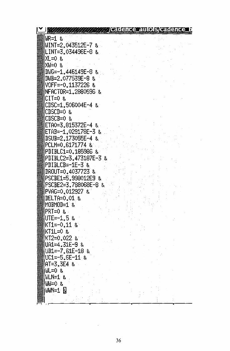
WR=1 & WINT=2.043512E-7 & LINT=3.034496E-8 & XL=O & XW=O & DWG=-1.446149E-8 & DWB=2.077539E-8 & VOFF=-0.1137226 & NFACTOR=1.2880596 & CIT=O & CDSC=1.506004E-4 & CDSCD=O & CDSCB=O & ETA0=3.815372E-4 & ETAB=-1.029178E-3 & DSUB=2.173055E-4 & PCLM=0.6171774 & PDIBLC1=0.185986 & PDIBLC2=3.473187E-3 & PDIBLCB=-1E-3 & DROUT=0.4037723 & PSCBE1=5.998012E9 & PSCBE2=3.788068E-8 & PVAG=0.012927 & DELTA=0.01 & MOBMOD=1 & PRT=O & UTE=-1.5 & KTl=-0.11 & KT1L=O & KT2=0.022 & UA1=4.31E-9 & UB1=-7.61E-18 & UC1=-5.6E-11 & AT=3.3E4 & WL=O & WLN=1 & WW=O & WWN=1 ~
36