
ANALOG-TO-DIGITAL CONVERTERS Dissertation Submitted to...
147
SINGLE-EVENT EFFECT MITIGATION IN PIPELINED ANALOG-TO-DIGITAL CONVERTERS By Brian D. Olson Dissertation Submitted to the Faculty of the Graduate School of Vanderbilt University in partial fulfillment of the requirements for the degree of DOCTOR OF PHILOSOPHY in Electrical Engineering December, 2010 Nashville, Tennessee Approved: Lloyd W. Massengill W. Timothy Holman Bharat L. Bhuva Arthur F. Witulski Dale McMorrow
Transcript of ANALOG-TO-DIGITAL CONVERTERS Dissertation Submitted to...
SINGLE-EVENT EFFECT MITIGATION IN PIPELINED
ANALOG-TO-DIGITAL CONVERTERS
By
Brian D. Olson
Dissertation
Submitted to the Faculty of the
Graduate School of Vanderbilt University
in partial fulfillment of the requirements
for the degree of
DOCTOR OF PHILOSOPHY
in
Electrical Engineering
December, 2010
Nashville, Tennessee
Approved:
Lloyd W. Massengill
W. Timothy Holman
Bharat L. Bhuva
Arthur F. Witulski
Dale McMorrow

ii
ACKNOWLEDGEMENTS
I would like to thank my advisor, Dr. Lloyd W. Massengill. With his guidance I
have achieved my degree. I would like to thank my other committee members,
Dr. W. Timothy Holman, Dr. Bharat L. Bhuva, Dr. Arthur F. Witulski, and
Dr. Dale McMorrow, for their encouragement, comments, and suggestions.
I am grateful for the support of Lew Cohn, Major Eric Heigel, Bruce Wilson, and
the Defense Threat Reduction Agency.
Finally, I would like to thank my family. My mother has always provided
positive encouragement as I reached for my goals. My father has an uncanny ability to
provide concise direction even when I have been lost. My brother has always been a
great example to follow. Most importantly I would like to thank my wife, Anna. She has
been an integral part of my life and has made me stronger. I am truly blessed to have her
in my life. Their constant support and motivation is something I will always admire.
iii
TABLE OF CONTENTS
Page ACKNOWLEDGEMENTS................................................................................................ ii LIST OF FIGURES ........................................................................................................... vi LIST OF TABLES............................................................................................................ xii Chapter
I. INTRODUCTION ...................................................................................................1 II. SINGLE-EVENT EFFECTS ...................................................................................4 Introduction........................................................................................................4 Radiation Environments.....................................................................................5 Trapped Radiation Environment..................................................................6 Solar .............................................................................................................8 Cosmic .......................................................................................................10 Terrestrial ...................................................................................................12 Basic Mechanisms of Single-Events................................................................13 Simulating Circuit Response to Single-Events ................................................16 Conclusion .......................................................................................................18 III. ANALOG-TO-DIGITAL CONVERTERS ...........................................................19 Introduction......................................................................................................19 Basic ADC Operation ......................................................................................19 Common ADC Performance Metrics...............................................................20 Common ADC Architectures...........................................................................22 Pipelined ADC.................................................................................................24 Topology....................................................................................................24 1.5-Bit Stage ..............................................................................................25 Multi-Bit Stage...........................................................................................27 Comparator ................................................................................................28 Multiplying Digital-to-Analog Converter..................................................30 Conclusion .......................................................................................................35 IV. SINGLE-EVENT EFFECTS IN PIPELINED ANALOG-TO-DIGITAL CONVERTERS ...............................................................................................36 Introduction......................................................................................................36
iv
Heavy Ion Testing............................................................................................36 SE Anlaysis......................................................................................................40 Pipelined ADCs .........................................................................................40 Flash ADCs................................................................................................41 SE Hardening...................................................................................................42 Conclusion .......................................................................................................43 V. FREQUENCY DOMAIN ANALYSIS .................................................................44 Introduction......................................................................................................44 Analysis Example: A Pipelined ADC..............................................................46 Operation....................................................................................................46 1.5-bit Stage Design...................................................................................47 Comparator Errors and Triple-Mode Redundancy ....................................49 Model Setup...............................................................................................50 10-Bit ADC Results ...................................................................................51 12-Bit and 14-Bit ADC Results .................................................................54 Upset Injection Rate...................................................................................55 Conclusion .......................................................................................................57 VI. MULTI-BIT STAGES...........................................................................................59 Introduction......................................................................................................59 Background......................................................................................................61 Single-Event Analysis of the Comparators......................................................63 SE-Response of 3-Input NAND Encoding Schemes.................................63 SE-Response of a More Robust Encoding Scheme ...................................65 SE-Simulations of the 3 Different Encoding Schemes..............................66 Single-Event Analysis of the MDAC ..............................................................72 SE-Response of the MDAC.......................................................................72 SE-Simulations of the MDAC ...................................................................73 Conclusion .......................................................................................................79 VII. SINGLE-EVENT EFFECT MITIGATION IN SWITCHED-CAPACITOR CIRCUITS .......................................................................................................80 Introduction to Dual-Path Hardening on a Comparator...................................80 Circuit Operation .............................................................................................83 Mitigation Technique.......................................................................................84 Analysis............................................................................................................89 Discussion........................................................................................................91 Results of the Dual Path RHBD Topology................................................91 Error Correction in Pipelined ADCs..........................................................93 Open Loop Versus Closed Loop Response ...............................................93 Tradeoffs ....................................................................................................96 Conclusions to Dual-Path Hardening on a Comparator...................................99
v
Introduction to Dual-Path Hardening Experimental Validation ....................100 Hardening Switched-Capacitor Circuits ........................................................102 Test Chip........................................................................................................104 Multiplying Digital-to-Analog Converter................................................104 Comparator ..............................................................................................106 Experimental Results .....................................................................................109 Conclusions to Dual-Path Hardening Experimental Validation ....................111 Introduction to Layout Considerations ..........................................................112 Background....................................................................................................113 Test Design and Circuit Operation ................................................................114 Results............................................................................................................117 Conclusion to Layout Considerations............................................................117 IX. CONCLUSIONS..................................................................................................121 Conclusion .....................................................................................................121 Design Techniques for SE-Hardened Pipelined ADCs .................................123 REFERENCES ................................................................................................................125

vi
LIST OF FIGURES Figure Page 1. In 1999, spacecraft anomaly records were categorized into anomaly types (ESD: electrostatic discharge; SEU: single event upset) [24] (data from [3]).........5 2. An illustration of the space radiation environment [25]. .........................................6 3. Motion of trapped charged particles in the Earth’s magnetic field [26], [27]. ........7 4. Equatorial radial profiles for proton fluxes [29]. .....................................................8 5. Correlation of proton events with solar cycle [30]. .................................................9 6. An EIT image in the 284 Angstrom wavelength of extreme UV light from each year of nearly an entire solar cycle [31]. .........................................................9 7. Particle flux data taken by ACE, SAMPEX, GOES-11 for a SEP [32].................10 8. Proton fluences from different SEP events [32]. ...................................................11 9. GCR relative ion composition [30], [33]. ..............................................................11 10. Neutrons flux increases with increasing flight altitude [2]....................................13 11. LET as a function of depth in silicon for a 132Xe ion with energy of 5 GeV. The range is about 520 µm and the maximum is referred to as the Bragg peak (from [40]).....................................................................................................14 12. Illustration of a diffusion region collecting the charge generated by a single-event. Regions of drift transport, depletion funnel, and diffusion transport are labeled (from [43])............................................................................15 13. Illustration showing the use of a current source to model a single-event in SPICE (from [47])..................................................................................................17 14. Measured diode current profiles caused by 5 MeV alpha particles incident on different size diodes (from [49]). The initial current spike is charge collection through drift, while the tail current is charge collection through diffusion. ................................................................................................................17 15. The ideal output response of a 3-bit ADC. ............................................................20
vii
16. An example of differential nonlinearity (DNL) in a 3-bit ADC............................22 17. An example of integral nonlinearity (INL) in a 3-bit ADC...................................23 18. Block diagram of an N-stage pipelined ADC. A 3-bit block diagram of a stage is also shown.................................................................................................26 19. Simplified pipelined ADC 1.5-bit stage architecture.............................................27 20. (a) The switched-capacitor comparator operates in two phases: (b) reset phase and (c) evaluation phase. .............................................................................29 21. The residue voltage transfer function for a 1.5-bit stage. ......................................31 22. The residue voltage transfer function for a 3-bit stage. .........................................32 23. Schematic of a multiplying digital-to-analog converter switched-capacitor network used in a 1.5-bit pipelined ADC stage. ....................................................33 24. Schematic of a multiplying digital-to-analog converter switched-capacitor network used in a 3-bit pipelined ADC stage. .......................................................34 25. Heavy ion testing results for the 12-bit 5 MSPS AD42961. Cross-section of all errors is plotted as well as errors only occurring in the 7 MSBs (re-plotted from [55]).............................................................................................37 26. Heavy ion testing results for the 12-bit 3 MSPS AD 1672 (from [56]).................38 27. Heavy ion testing results for the 12-bit 3 MSPS AD9223. Error cross- section in the 7 MSBs and 4 MSBs are shown (re-plotted from [57]). .................39 28. Heavy ion testing results for the 14-bit 105 MSPS ADS5424 (from [59]). ..........39 29. Simplified pipelined ADC architecture. ................................................................46 30. Simplified pipelined ADC 1.5-bit stage architecture.............................................47 31. Example FFT of C++ pipelined ADC model using 220 simulated samples...........51 32. Example FFT of C++ pipelined ADC model with injected comparator upsets. A single comparator had a probability of 0.1% to upset during a sample. The simulation used 220 simulated samples.............................................51 33. Signal-to-noise ratio improvement for increasing use of comparator TMR in a 10-bit pipelined ADC. The results shown are for a model with an individual comparator upset probability of 0.1%. .................................................52
viii
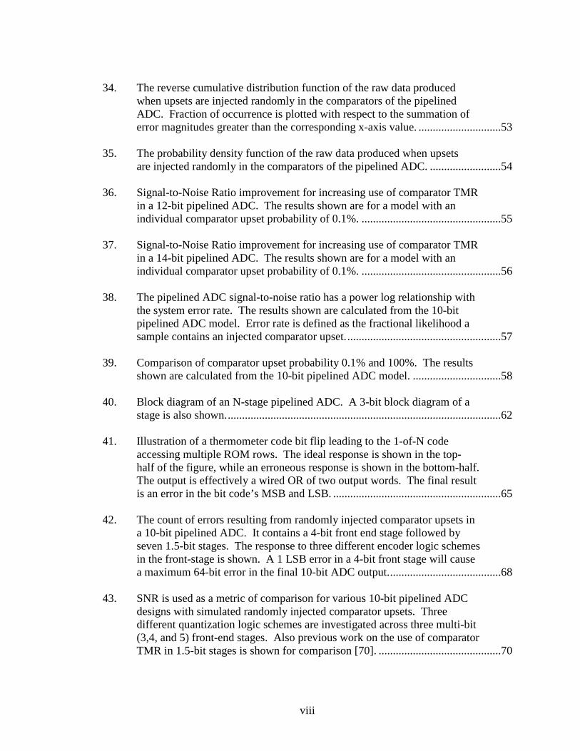
34. The reverse cumulative distribution function of the raw data produced when upsets are injected randomly in the comparators of the pipelined ADC. Fraction of occurrence is plotted with respect to the summation of error magnitudes greater than the corresponding x-axis value. .............................53 35. The probability density function of the raw data produced when upsets are injected randomly in the comparators of the pipelined ADC. .........................54 36. Signal-to-Noise Ratio improvement for increasing use of comparator TMR in a 12-bit pipelined ADC. The results shown are for a model with an individual comparator upset probability of 0.1%. .................................................55 37. Signal-to-Noise Ratio improvement for increasing use of comparator TMR in a 14-bit pipelined ADC. The results shown are for a model with an individual comparator upset probability of 0.1%. .................................................56 38. The pipelined ADC signal-to-noise ratio has a power log relationship with the system error rate. The results shown are calculated from the 10-bit pipelined ADC model. Error rate is defined as the fractional likelihood a sample contains an injected comparator upset.......................................................57 39. Comparison of comparator upset probability 0.1% and 100%. The results shown are calculated from the 10-bit pipelined ADC model. ...............................58 40. Block diagram of an N-stage pipelined ADC. A 3-bit block diagram of a stage is also shown.................................................................................................62 41. Illustration of a thermometer code bit flip leading to the 1-of-N code accessing multiple ROM rows. The ideal response is shown in the top- half of the figure, while an erroneous response is shown in the bottom-half. The output is effectively a wired OR of two output words. The final result is an error in the bit code’s MSB and LSB. ...........................................................65 42. The count of errors resulting from randomly injected comparator upsets in a 10-bit pipelined ADC. It contains a 4-bit front end stage followed by seven 1.5-bit stages. The response to three different encoder logic schemes in the front-stage is shown. A 1 LSB error in a 4-bit front stage will cause a maximum 64-bit error in the final 10-bit ADC output........................................68 43. SNR is used as a metric of comparison for various 10-bit pipelined ADC designs with simulated randomly injected comparator upsets. Three different quantization logic schemes are investigated across three multi-bit (3,4, and 5) front-end stages. Also previous work on the use of comparator TMR in 1.5-bit stages is shown for comparison [70]. ...........................................70
ix
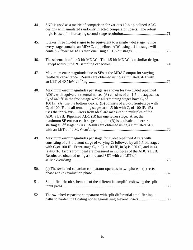
44. SNR is used as a metric of comparison for various 10-bit pipelined ADC designs with simulated randomly injected comparator upsets. The robust logic is used for increasing second-stage resolution..............................................71 45. It takes three 1.5-bit stages to be equivalent to a single 4-bit stage. Since every stage contains an MDAC, a pipelined ADC using a 4-bit stage will contain 2 fewer MDACs than one using all 1.5-bit stages. ...................................73 46. The schematic of the 3-bit MDAC. The 1.5-bit MDAC is a similar design, Except without the 2C sampling capacitors...........................................................74 47. Maximum error magnitude due to SEs at the MDAC output for varying feedback capacitance. Results are obtained using a simulated SET with an LET of 40 MeV-cm2/mg. ..................................................................................75 48. Maximum error magnitudes per stage are shown for two 10-bit pipelined ADCs with equivalent thermal noise. (A) consists of all 1.5-bit stages, has Cf of 440 fF in the front-stage while all remaining stages have Cf of 100 fF. (A) use the bottom x-axis. (B) consists of a 3-bit front-stage with Cf of 100 fF and all remaining stages are 1.5-bit with Cf of 100 fF. (B) uses the top x-axis. Errors from ideal are measured in multiples of the ADC’s LSB. Pipelined ADC (B) has one fewer stage. Also, the maximum SE error at each stage output in (B) is equivalent to errors starting at 2nd stage in (A). Results are obtained using a simulated SET with an LET of 40 MeV-cm2/mg. ..........................................................................76 49. Maximum error magnitudes per stage for 10-bit pipelined ADCs with consisting of a 3-bit front-stage of varying Cf followed by all 1.5-bit stages with Cf of 100 fF. Front-stage Cf in 2) is 100 fF, in 3) is 220 fF, and in 4) is 440 fF. Errors from ideal are measured in multiples of the ADC’s LSB. Results are obtained using a simulated SET with an LET of 40 MeV-cm2/mg.....................................................................................................78 50. (a) The switched-capacitor comparator operates in two phases: (b) reset phase and (c) evaluation phase. .............................................................................82 51. Simplified circuit schematic of the differential amplifier showing the split input paths..............................................................................................................85 52. The switched-capacitor comparator with split differential amplifier input paths to harden the floating nodes against single-event upsets..............................86
x
53. Currents through the differential input transistors during a single-event strike during the evaluation phase. The differential input voltage to the comparator pre-amp was 75 mV and the single-event deposited 23 fC on the floating node VPA_A+. Even though M1A is forced off, the dual path RHBD technique preserves the correct response, since the increase in current through M1B remains greater than the sum of currents through M2A and M2B. The comparator will latch the correct logic state. ........................88 54. Currents through the differential input transistors during a single-event strike during the evaluation phase. The differential input voltage to the comparator pre-amp was 45 mV and the single-event deposited 23 fC on the floating node VPA_A+. In this case the total current through the M1A and M1B remained less than the total current through M2A and M2B post strike, resulting in the latching of an incorrect logic state. Clearly, the dual path RHBD technique cannot prevent errors if the pre-amp input voltage is too small. ...............................................................................................89 55. Contour plots of differential pre-amp input voltage vs. deposited charge for (a) standard SC comparator design, (b) standard design with doubled capacitor size, and (c) splitting the comparator input nodes..................................92 56. Total currents through the differential input branches of using quad-path RHBD during a single-event strike. The single-event and operating conditions were the same as Fig. 54. The differential input to the comparator pre-amp was 45 mV and the single-event deposited 23 fC on the floating node VPA_A+. Unlike in Fig. 54 in which the dual-path RHBD did not work, the current through the M1 branch of the quad-path does return to being greater than the current through the M2 branch. The comparator will latch the correct logic state. .........................................................95 57. The result of the proposed RHBD technique applied to four parallel paths per input. ................................................................................................................96 58. The completed layout designs for (a) baseline and (b) RHBD comparator. The process used is the IBM CMOS 9SF. .............................................................97 59. The (a) switching network and (b) differential input for a basic sample- and-hold amplifier................................................................................................101 60. The dual-path hardening technique doubles the OTA input path in the (a) switching network and (b) OTA. .........................................................................103 61. Schematic of the baseline, 2X gain, multiplying digital-to-analog converter switched-capacitor network. ................................................................105 62. Micrograph of the baseline and hardened MDACs. ............................................107
xi
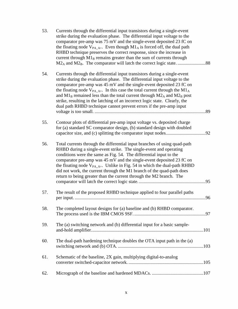
63. Schematic of the baseline comparator switched-capacitor network. ...................107 64. Micrograph of the baseline and hardened comparators. ......................................108 65. Test results for baseline and hardened MDAC. ...................................................109 66. Test results for baseline and hardened comparator. Comparator errors below the plotted dashed lined will be corrected in a pipelined analog-to- digital converter. ..................................................................................................110 67. Illustration of single-ended and fully differential operation. An injected transient on a single-ended amplifier will be propagated with the signal while a transient shared by the inputs of a fully-differential amplifier will be cancelled..........................................................................................................113 68. Proposed charge-sharing layout designs RHBL M1 (top) and RHBL M2 (bottom)................................................................................................................115 69. Schematic of test circuit and the RHBL M2 layout.............................................116 70. Baseline case of charge collection on a single transistor without the effects of charge sharing for M1 and M2.............................................................118 71. Unique charge for M1 (top) and M2 (bottom).....................................................119

xii
LIST OF TABLES
Table Page 1. Output states of the ADC pipelined stage decoder................................................48 2. Sensitive areas collecting unique charge greater than half of the maximum deposited charge for baseline and rhbl M1 and M2.............................................120
1
CHAPTER I
INTRODUCTION
Analog-to-digital converters (ADCs) are necessary circuits in many space,
military, and medical circuit applications. Intelligence, surveillance, reconnaissance, and
communication missions all require high performance ADCs. Speed, resolution, and
power are concerns in high performance designs. Unlike commercial applications, space,
military, and some medical electronics must also be able to function in a radiation
environment [1]-[5]. This additional complexity magnifies an interesting and needed
area of research.
One type of radiation effect can occur when a single ionizing particle passes
through the microelectronic circuit. An ionizing particle will generate charge in
semiconductor materials in the form of electron-hole pairs. The positive carriers, holes,
and negative carriers, electrons, may harmlessly recombine, but may also be collected on
circuit nodes causing erroneous current and voltage perturbations in the circuit operation.
An electrical change in transistor operation caused by an ionizing particle is called a
single-event effect (SEE). A single-event upset (SEU) occurs when an SEE causes a flip
in a logic state. A single-event transient (SET) is a current and/or voltage perturbation,
and if sufficient in size may propagate through logic.
Ionizing particles can be found at high altitudes, space, and in some medical
applications. Also, ionizing particles can be created as secondary or tertiary particles
from neutron collisions with other atoms. Single-events can disrupt ADC operation
2
producing erroneous output codes. One of the first heavy-ion irradiation tests of an ADC
showed that low LET particles will cause a complex distribution of errors [6]. The errors
occur in small-magnitude Gaussian-like distributions around the expected output code,
and also large magnitude errors [6], i.e., codes far from their expected values. In a
follow-up analysis these error types were categorized as a noise component (small
magnitude) and offset (large magnitude) [7]. The single-event error response of ADCs
can be much more complicated than noise and offset errors. Temporary data errors,
lingering offset errors, zero outputs, and linearity issues all occurred in a different ADC
heavy ion test [8]. Even the ADC response to proton testing provided a complex
response including a non-linear error response seen to occur over sample-rate and upsets
lasting multiple clock cycles [9]. Laser testing has shown some upsets internal to an
ADC can be masked while others can exacerbate large output errors [10], [11]. The
complex ADC responses to heavy ions including error magnitudes, rates, and duration
have been seen in other tests as well [12], [13].
The goal of this dissertation is to understand SEEs in high-speed ADCs, so the
impact of design topologies and mitigation techniques can be evaluated for Department
of Defense (DOD) or commercial space deployment. This goal can be broken into two
parts. The first part is to characterize and explain the single event effect response. The
second part is to provide additional circuit design alternatives that improve SEE response.
These goals address a need in the radiation effects community as discussed in the survey
performed by Kenneth G. Merkel and Anthony L. Wilson in the 2003 IEEE Proceedings
of the Aerospace Conference [14]. The survey concluded that defense space applications
have a need for radiation tolerant ADCs of speeds of at least 25 Msps with bit resolutions
3
of at least 10-12 bits, specifications best suited for the pipelined ADC architecture. The
work in this dissertation focuses on the pipelined ADC sub-circuits along the signal path.
Digital latches, references, bias circuits, and clock circuits are also known to be sensitive
to single-events [1], [13], [15]-[17], but are assumed to be independently hardened. The
conclusion of this work will help designers achieve ADCs for the next generation
applications, influence experimental testing methodologies, and be applied to other high-
speed mixed signal applications.
4
CHAPTER II
SINGLE-EVENT EFFECTS
Introduction
Space and military circuit applications must operate in a more intense radiation
environment than commercial electronics on Earth. For this reason careful design and
testing must be take place before fielding. This work focuses on one type of radiation
event called single-event effects. In this case a single ionizing particle passes through the
microelectronic circuit generating excess electron-hole pairs. Unless proper precaution is
taken, an erroneous circuit response can occur from devices collecting electron and/or
hole pairs.
SEEs in microelectronics were first theorized in 1962 [18]. In 1967, one-
dimensional numerical modeling showed a SEE can cause a memory error called a
single-event upset (SEU) [19], [20]. A SEU was not observed until almost a decade later.
In 1975, the first published account of a single event upset occurring in space was
reported [21]. A few years later, 1979, the first SEU in a random access memory was
published [1].
SEEs have become a more prevalent issue due to CMOS scaling. In 1965, G. E.
Moore proposed that the number of transistors on a chip would double every two years
[22]. Since then this statement has become the benchmark for the commercial
semiconductor industry and has become famously known as Moore’s Law. In order to
keep pace with Moore’s Law, industry has decreased device dimensions, operating
5
voltage, gate oxide thickness, gate length, nodal separation of the devices, nodal
capacitance, etc. with every technology generation. Since 1965, consumers have enjoyed
the benefits of significant increases in performance and speed, decrease in integrated
circuit cost, and smaller chips with greater functionality for CMOS technology.
Unfortunately, these factors have a negative impact of increased SE vulnerability of
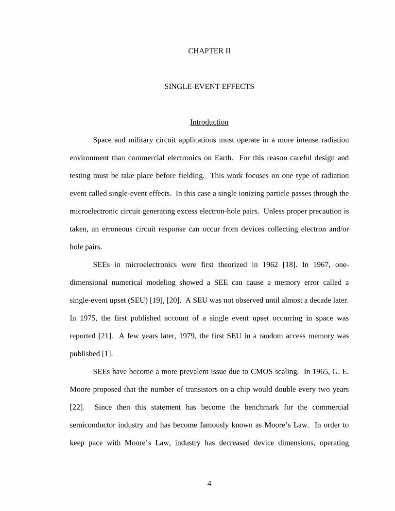
microelectronics [23]. In 1999, 28% of spacecraft anomaly records were attributed to
SEEs as shown by Fig. 1 [3], [24].
Radiation Environments
A detailed understanding of the radiation is required at the start of any radiation-
hardened circuit design. The distribution of ionizing particles that interact with a space
system is dependent on orbit altitude or space flight path. The space radiation
Fig. 1. In 1999, spacecraft anomaly records were categorized into anomaly types (ESD: electrostatic discharge; SEU: single event upset) [24] (data from [3]).

6
environment is broken into three categories: trapped, solar, and cosmic, and is illustrated
in Fig. 2 [25]. On Earth, neutron collisions with other atoms can produce ionizing
particle recoils; an issue for any flight application. Also there is a history of radioactive
contaminants in the microelectronics industry, which have to be carefully screened before
fabrication or SEEs will result.
Trapped Radiation Environment
There is an abundance of charged particles, predominantly protons and electrons,
trapped by the Earth’s magnetic fields. These regions of trapped particles were first
discovered and published by J. A. Van Allen in 1959, and thus subsequently named the
Van Allen belts [26]. Trapped protons and electrons are reflected back and forth between
Earth’s magnetic poles traveling along the magnetic field contours, and at the same time
Fig. 2. An illustration of the space radiation environment [25].

7
the trapped particles will also revolve around the Earth: electrons drift eastward while
protons drift westward. Trapped charged particle motion is illustrated in Fig. 3 [27], [28].
High altitude and space missions are impacted by trapped protons and electrons.
Protons are capable of producing SEEs through either direct or indirect ionization;
electrons are not yet able to produce SEEs in current technology. Electrons contribute to
total ionizing dose (TID), another well-studied radiation effect, but TID effects are not
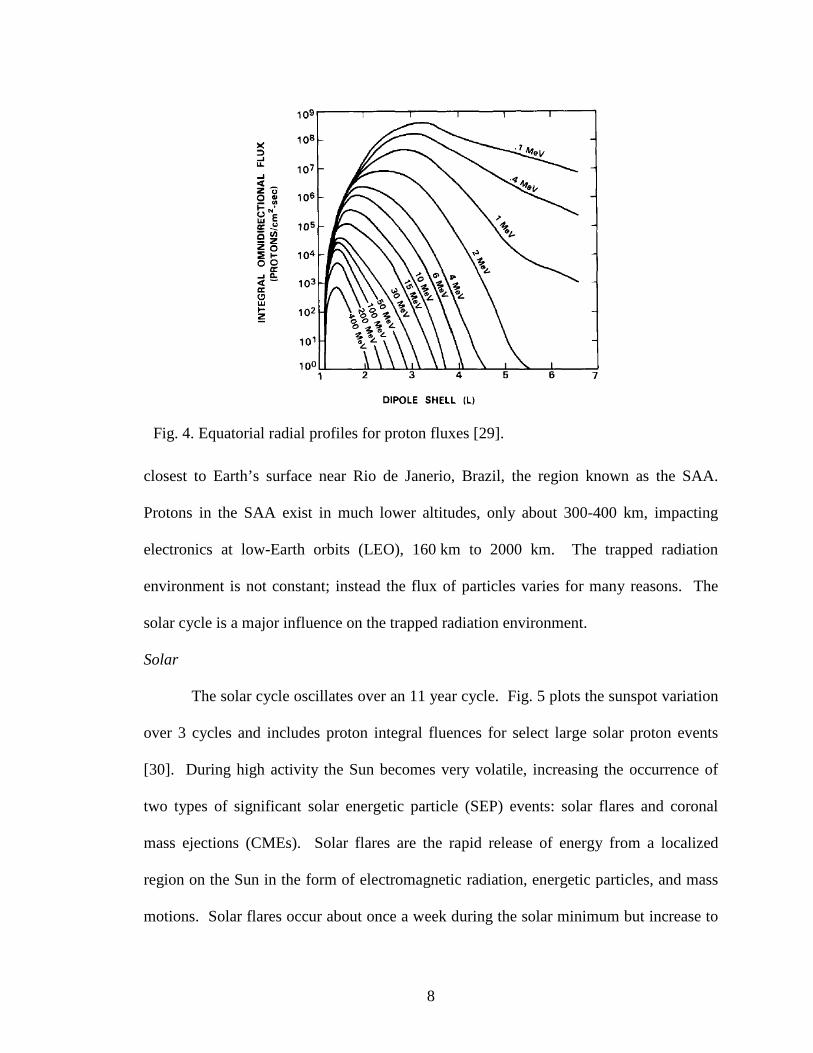
covered in this work. Fig. 4 shows proton fluxes for different energies as a function of
L-shell number (distance measured in Earth-radii from Earth’s center) [29]. Trapped
protons across a wide range of energies can impact electronics at mid-Earth orbits
(MEO), 2000 km to 35,000 km, corresponding to L-shells 1.3 through 6.5. At
geosynchronous Earth orbit (GEO), 35,786 km, and at further high-Earth orbits (HEO),
trapped proton fluxes are dominated by low energy protons (< 1 MeV). Another area of
proton concentration is the South Atlantic Anomaly (SAA). Earth’s magnetic poles are
offset from the rotational axis by 11 degrees. Due to this offset, the Van Allen belts are
Fig. 3. Motion of trapped charged particles in the Earth’s magnetic field [27], [28].
8
closest to Earth’s surface near Rio de Janerio, Brazil, the region known as the SAA.
Protons in the SAA exist in much lower altitudes, only about 300-400 km, impacting
electronics at low-Earth orbits (LEO), 160 km to 2000 km. The trapped radiation
environment is not constant; instead the flux of particles varies for many reasons. The
solar cycle is a major influence on the trapped radiation environment.
Solar
The solar cycle oscillates over an 11 year cycle. Fig. 5 plots the sunspot variation
over 3 cycles and includes proton integral fluences for select large solar proton events
[30]. During high activity the Sun becomes very volatile, increasing the occurrence of
two types of significant solar energetic particle (SEP) events: solar flares and coronal
mass ejections (CMEs). Solar flares are the rapid release of energy from a localized
region on the Sun in the form of electromagnetic radiation, energetic particles, and mass
motions. Solar flares occur about once a week during the solar minimum but increase to
Fig. 4. Equatorial radial profiles for proton fluxes [29].

9
Fig 6. An EIT image in the 284 Angstrom wavelength of extreme UV light from each year of nearly an entire solar cycle [31].
Fig 5. Correlation of proton events with solar cycle [30].
10
several per day when the Sun is most active. CME is the result of a huge magnetic
bubble of plasma that erupts from the Sun’s corona. During solar minimum, CMEs occur
about once every other day; at solar maximum, CMEs will occur 5-6 times a day. Solar
flares and CMEs can also occur simultaneously. Fig. 6 is a sequence of images of the
Sun spanning an entire solar cycle from the Solar and Heliospheric Observatory [31]. In
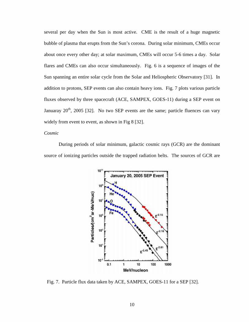
addition to protons, SEP events can also contain heavy ions. Fig. 7 plots various particle
fluxes observed by three spacecraft (ACE, SAMPEX, GOES-11) during a SEP event on
Januaray 20th, 2005 [32]. No two SEP events are the same; particle fluences can vary
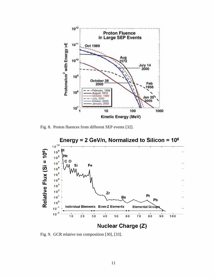
widely from event to event, as shown in Fig 8 [32].
Cosmic
During periods of solar minimum, galactic cosmic rays (GCR) are the dominant
source of ionizing particles outside the trapped radiation belts. The sources of GCR are
Fig. 7. Particle flux data taken by ACE, SAMPEX, GOES-11 for a SEP [32].
11
Fig. 9. GCR relative ion composition [30], [33].
Fig. 8. Proton fluences from different SEP events [32].

12
mostly unknown, but possible origins are theorized to be the Big Bang and supernovas.
Since GCR originate from outside our solar system, particle trajectories are essentially
omnidirectional. GCR distributions are dominated by protons; the flux of protons is
approximately 10 times larger than then next particle, helium, and over 1000 times larger
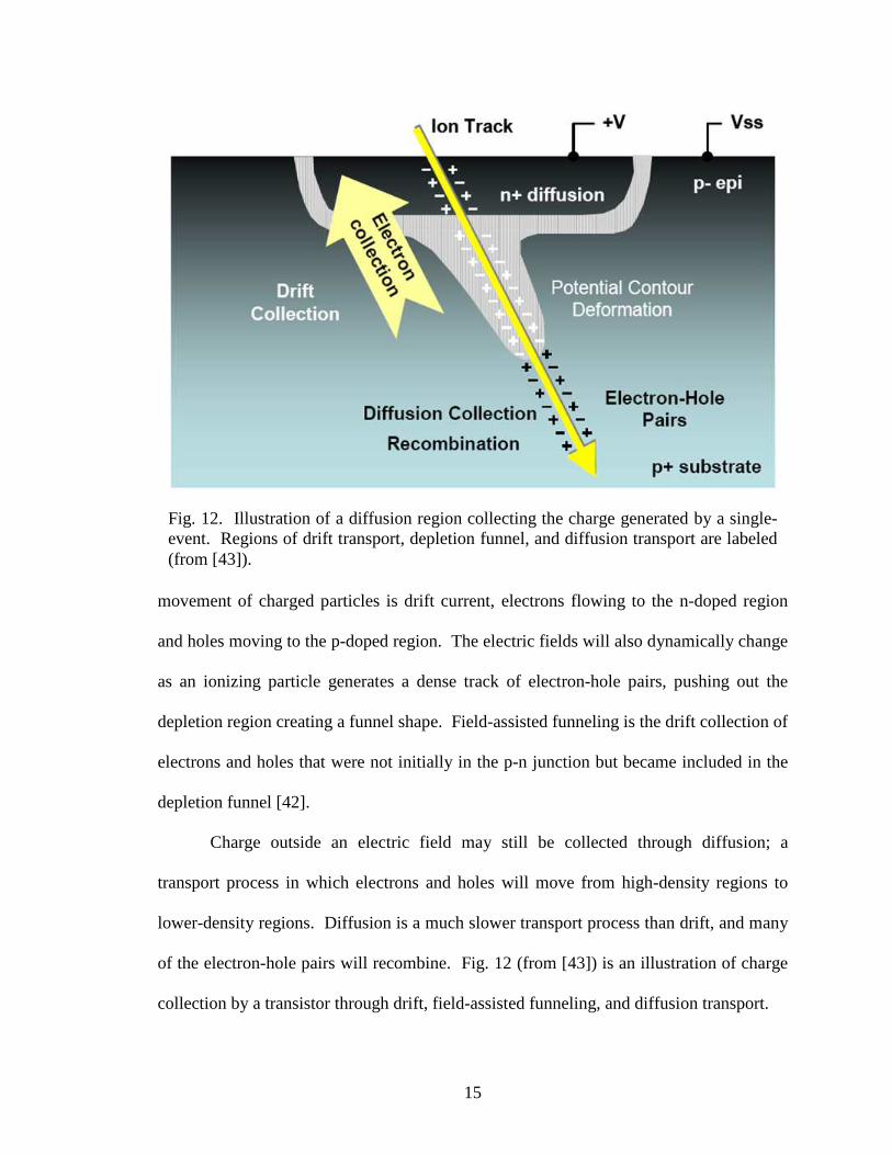
than iron. Fig. 9 plots the relative flux of ions with an energy of 2 GeV/nucleon that
make up GCRs, and has been normalized to Si flux of 106 [30], [33].
Terrestrial
Particle collisions between the Earth’s atmosphere and high energy GCRs or solar
particles can produce neutrons. Unlike protons and heavy ions, neutrons do not cause
direct ionization, but are one of the main sources of SEEs within the Earth’s atmosphere.
Energetic neutrons can interact with nuclei elastically, displacing the nucleus from its
lattice position, or inelastically, causing the nucleus to eject ionizing particles. Terrestrial
neutrons are the products of multi-generational particle collisions. Neutrons are an issue
at flight altitudes, as shown in Fig. 10 [2], and due to the shape of the magnetic fields,
GCRs can reach lower altitudes near the poles, resulting in a 5X-6X increase in the
number of neutrons [2]. Neutron flux is also dependent on the 11 year solar cycle and
can vary as much as a factor of two.
Impurities in the IC industry also account for terrestrial sources of SEEs. Alpha
particle emitters have been a concern for many years. In the late 1970s trace uranium and
thorium impurities were discovered to be the dominant cause of soft errors in dynamic
random-access memories (DRAMs) [34]. Currently, lead-solder is a common source of
alpha particles and has to be screened before use in IC packaging [35]. Another example
of impurities in the packaging and fabrication process causing SEEs, is the boron isotope

13
10B. Boron is commonly used as a p-type dopant and for borophosphosilicate glass
(BPSG), an insulator between metal layers. Boron has two isotopes: 80% of boron
particles are 11B while 20% are 10B. If 10B absorbs a neutron, it will become unstable,
breaking apart and releasing Li and an alpha particle, resulting in a increase in soft error
rates [36], [37]. The industry now screens boron for the 10B isotope, to minimize SEEs.
Basic Mechanisms of Single-Events
A single-event effect occurs when a sensitive device, such as a transistor, collects
the charge generated by an ionizing particle. As an ionizing particle passes through a
semiconductor it will lose energy to the material. This energy can excite electrons,
through Coulombic interaction, to break away from their valance bands leaving behind
vacancies (holes), thus generating electron-hole pairs (charge). The particle’s energy loss
is typically parameterized in the radiation effects community using linear energy transfer
Fig. 10. Neutrons flux increases with increasing flight altitude [2].

14
(LET). A minimum of 3.6 eV (Ee-h) is necessary to generate an electron-hole pair in
silicon [38]. LET can roughly be converted to charge generation per path length,
he
Si
E
XLETq
dX
dQ
−
⋅⋅=
)(ρ, (1)
given a silicon density (ρSi) of 2328 mg/cm3 and an electron energy (q) of 1.6x10⁻¹⁹ C
[38], [39]. An ionizing particle that has a constant LET of 10 MeV-cm2/mg will generate
100 fC/µm. However, ionizing particles do not lose energy at a constant rate. Fig. 11
shows the LET of 5 GeV 132Xe as a function of distance through silicon [40].
Without any external forces, electron-hole pairs will harmlessly recombine.
However, integrated CMOS circuits contain billions of p-n doping junctions, many of
which will be reversed biased. Electron-hole pairs generated in the depletion regions of
the reversed biased p-n junctions will quickly be separated by the electric fields. This
Fig. 11. LET as a function of depth in silicon for a 132Xe ion with energy of 5 GeV. The range is about 520 µm and the maximum is referred to as the Bragg peak (from [40]).
15
movement of charged particles is drift current, electrons flowing to the n-doped region
and holes moving to the p-doped region. The electric fields will also dynamically change
as an ionizing particle generates a dense track of electron-hole pairs, pushing out the
depletion region creating a funnel shape. Field-assisted funneling is the drift collection of
electrons and holes that were not initially in the p-n junction but became included in the
depletion funnel [42].
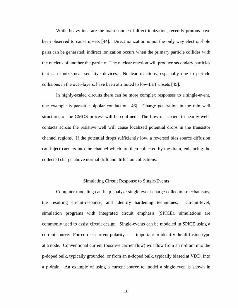
Charge outside an electric field may still be collected through diffusion; a
transport process in which electrons and holes will move from high-density regions to
lower-density regions. Diffusion is a much slower transport process than drift, and many
of the electron-hole pairs will recombine. Fig. 12 (from [43]) is an illustration of charge
collection by a transistor through drift, field-assisted funneling, and diffusion transport.
Fig. 12. Illustration of a diffusion region collecting the charge generated by a single-event. Regions of drift transport, depletion funnel, and diffusion transport are labeled (from [43]).
16
While heavy ions are the main source of direct ionization, recently protons have
been observed to cause upsets [44]. Direct ionization is not the only way electron-hole
pairs can be generated; indirect ionization occurs when the primary particle collides with
the nucleus of another the particle. The nuclear reaction will produce secondary particles
that can ionize near sensitive devices. Nuclear reactions, especially due to particle
collisions in the over-layers, have been attributed to low-LET upsets [45].
In highly-scaled circuits there can be more complex responses to a single-event,
one example is parasitic bipolar conduction [46]. Charge generation in the thin well
structures of the CMOS process will be confined. The flow of carriers to nearby well-
contacts across the resistive well will cause localized potential drops in the transistor
channel regions. If the potential drops sufficiently low, a reversed bias source diffusion
can inject carriers into the channel which are then collected by the drain, enhancing the
collected charge above normal drift and diffusion collections.
Simulating Circuit Response to Single-Events
Computer modeling can help analyze single-event charge collection mechanisms,
the resulting circuit-response, and identify hardening techniques. Circuit-level,
simulation programs with integrated circuit emphasis (SPICE), simulations are
commonly used to assist circuit design. Single-events can be modeled in SPICE using a
current source. For correct current polarity, it is important to identify the diffusion-type
at a node. Conventional current (positive carrier flow) will flow from an n-drain into the
p-doped bulk, typically grounded, or from an n-doped bulk, typically biased at VDD, into
a p-drain. An example of using a current source to model a single-even is shown in
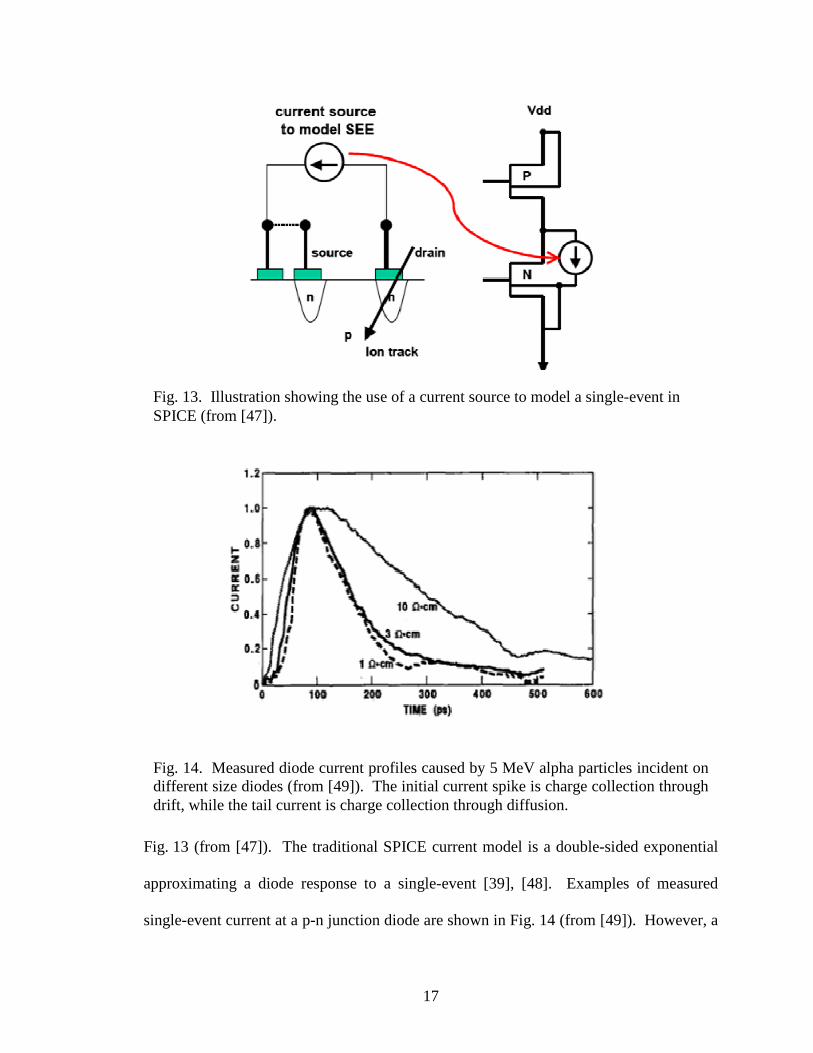
17
Fig. 13 (from [47]). The traditional SPICE current model is a double-sided exponential
approximating a diode response to a single-event [39], [48]. Examples of measured
single-event current at a p-n junction diode are shown in Fig. 14 (from [49]). However, a
Fig. 14. Measured diode current profiles caused by 5 MeV alpha particles incident on different size diodes (from [49]). The initial current spike is charge collection through drift, while the tail current is charge collection through diffusion.
Fig. 13. Illustration showing the use of a current source to model a single-event in SPICE (from [47]).
18
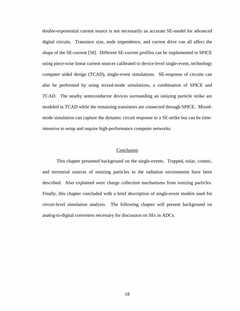
double-exponential current source is not necessarily an accurate SE-model for advanced
digital circuits. Transistor size, node impendence, and current drive can all affect the
shape of the SE-current [50]. Different SE-current profiles can be implemented in SPICE
using piece-wise linear current sources calibrated to device-level single-event, technology
computer aided design (TCAD), single-event simulations. SE-response of circuits can
also be performed by using mixed-mode simulations, a combination of SPICE and
TCAD. The nearby semiconductor devices surrounding an ionizing particle strike are
modeled in TCAD while the remaining transistors are connected through SPICE. Mixed-
mode simulation can capture the dynamic circuit response to a SE-strike but can be time-
intensive to setup and require high-performance computer networks.
Conclusion
This chapter presented background on the single-events. Trapped, solar, cosmic,
and terrestrial sources of ionizing particles in the radiation environment have been
described. Also explained were charge collection mechanisms from ionizing particles.
Finally, this chapter concluded with a brief description of single-event models used for
circuit-level simulation analysis. The following chapter will present background on
analog-to-digital converters necessary for discussion on SEs in ADCs.
19
CHAPTER III
ANALOG-TO-DIGITAL CONVERTERS
Introduction
Given the real-world environment is inherently analog, and the majority of
integrated chip (IC) processing is digital, analog-to-digital converters (ADCs) are
required to interface the two domains. Intelligence, surveillance, reconnaissance, and
communication missions all require high performance ADCs. This chapter explains basic
ADC operation, introduces the common performance metrics, and concludes with a
discussion on the pipelined ADC architecture.
Basic ADC Operation
An ADC converts a continuous analog signal into discrete digital values [51].
Typically, the output of an ADC is in binary; the total number of output bits is defined as
resolution. Therefore a 1-bit ADC will have 2 possible discrete values, a 2-bit ADC will
have 4 possible discrete values, a 3-bit ADC will have 8 possible discrete values, and so
forth. The least significant bit (LSB) of the binary output is the smallest unit step size
and is equal to full input range divided by the number of discrete values. Distances
between output codes are often measured in terms of LSBs. There are many types of
ADCs with resolutions as little as 1-bit to larger than 20-bits. The ADC’s conversion
speed is given in terms of the number of samples-per-second; typical speeds range from
20
kilo-samples-per-second (ksps), to mega-samples-per-second (Msps), and even giga-
samples-per-second (Gsps).
Common ADC Performance Metrics
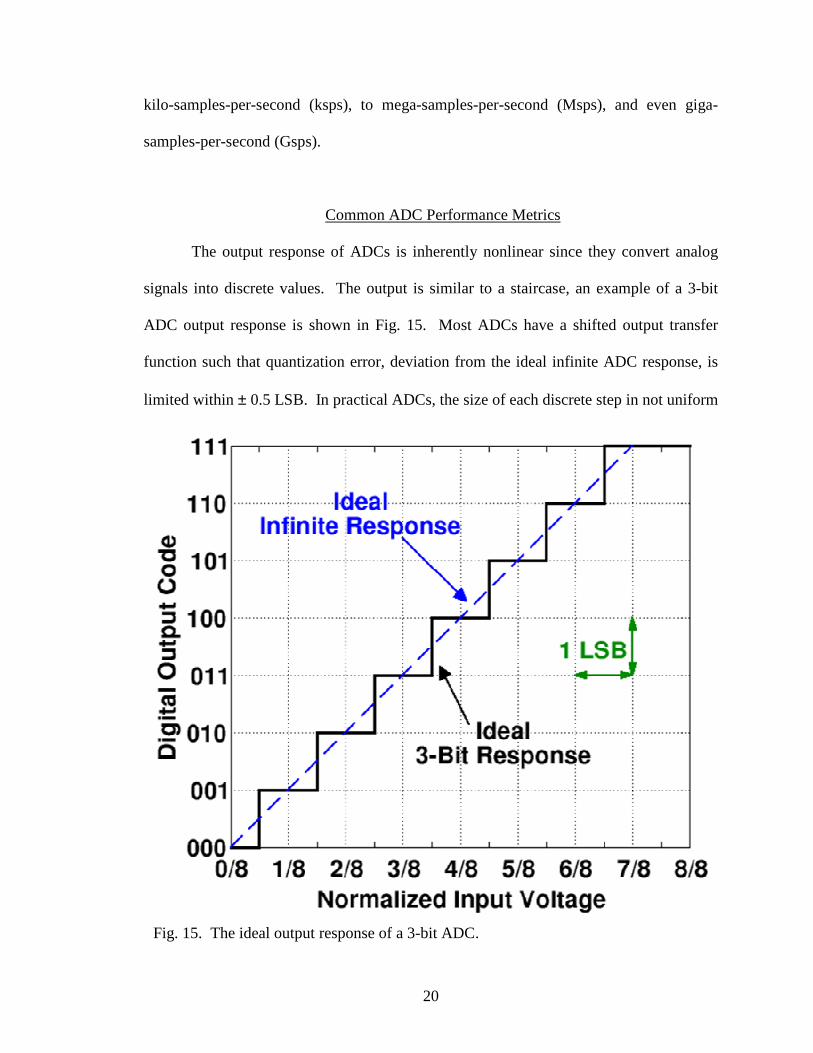
The output response of ADCs is inherently nonlinear since they convert analog
signals into discrete values. The output is similar to a staircase, an example of a 3-bit
ADC output response is shown in Fig. 15. Most ADCs have a shifted output transfer
function such that quantization error, deviation from the ideal infinite ADC response, is
limited within ± 0.5 LSB. In practical ADCs, the size of each discrete step in not uniform
Fig. 15. The ideal output response of a 3-bit ADC.
21
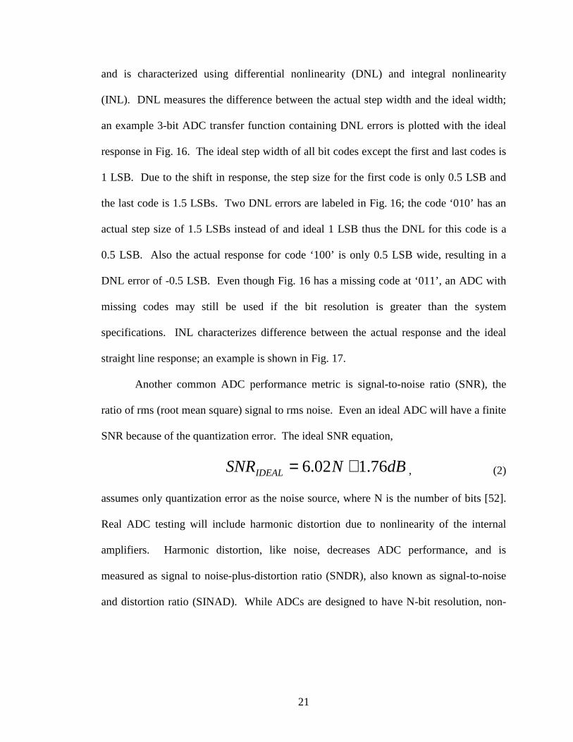
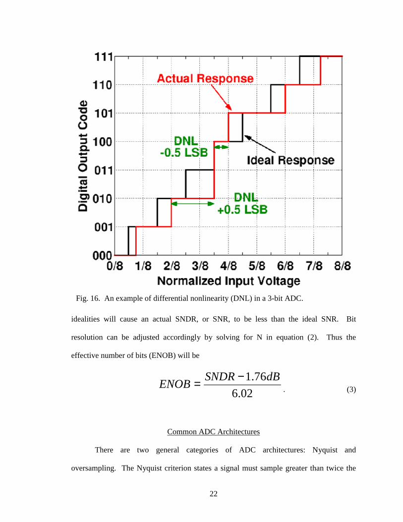
and is characterized using differential nonlinearity (DNL) and integral nonlinearity
(INL). DNL measures the difference between the actual step width and the ideal width;
an example 3-bit ADC transfer function containing DNL errors is plotted with the ideal
response in Fig. 16. The ideal step width of all bit codes except the first and last codes is
1 LSB. Due to the shift in response, the step size for the first code is only 0.5 LSB and
the last code is 1.5 LSBs. Two DNL errors are labeled in Fig. 16; the code ‘010’ has an
actual step size of 1.5 LSBs instead of and ideal 1 LSB thus the DNL for this code is a
0.5 LSB. Also the actual response for code ‘100’ is only 0.5 LSB wide, resulting in a
DNL error of -0.5 LSB. Even though Fig. 16 has a missing code at ‘011’, an ADC with
missing codes may still be used if the bit resolution is greater than the system
specifications. INL characterizes difference between the actual response and the ideal
straight line response; an example is shown in Fig. 17.
Another common ADC performance metric is signal-to-noise ratio (SNR), the
ratio of rms (root mean square) signal to rms noise. Even an ideal ADC will have a finite
SNR because of the quantization error. The ideal SNR equation,
dBNSNRIDEAL 76.102.6 += , (2)
assumes only quantization error as the noise source, where N is the number of bits [52].
Real ADC testing will include harmonic distortion due to nonlinearity of the internal
amplifiers. Harmonic distortion, like noise, decreases ADC performance, and is
measured as signal to noise-plus-distortion ratio (SNDR), also known as signal-to-noise
and distortion ratio (SINAD). While ADCs are designed to have N-bit resolution, non-
22
idealities will cause an actual SNDR, or SNR, to be less than the ideal SNR. Bit
resolution can be adjusted accordingly by solving for N in equation (2). Thus the
effective number of bits (ENOB) will be
02.6
76.1 dBSNDRENOB
−= . (3)
Common ADC Architectures
There are two general categories of ADC architectures: Nyquist and
oversampling. The Nyquist criterion states a signal must sample greater than twice the
Fig. 16. An example of differential nonlinearity (DNL) in a 3-bit ADC.

23
maximum signal frequency in order for the original signal to be recoverable. ADCs that
sample near the Nyquist criterion are considered Nyquist-rate converters. A design
challenge for these converters is aliasing; signals with higher frequencies than the
bandwidth of the ADC are indistinguishable from the signals inside the ADC’s
bandwidth. The frequency of an aliased signal is the difference between the high-
frequency component and the ADC’s sampling rate. Nyquist-rate converters require an
anti-aliasing filter with a sharp cutoff frequency at half the sampling frequency to prevent
high frequency signals from corrupting the data. In some applications, the anti-aliasing
filter requirements are relaxed by oversampling. Resolution can be increased by 0.5 bit
Fig 17. An example of integral nonlinearity (INL) in a 3-bit ADC.
24
for every 2X increase in sampling speed. Oversampling converters often have high
resolution but due to the oversampling ratio the maximum signal frequency is lower than
Nyquist-rate converters.
There are many types of ADC architectures; each having its own typical range of
resolution and speed often determining the application. Flash ADCs can operate at Gsps
speeds, but will have a maximum resolution of 8-bits. This architecture uses a ladder
structure of comparators, each ladder rung providing an additional quantization level.
Successive-approximation ADCs can quantize 20 or more bits but have slow sampling
speeds on the order of ksps. This architecture uses an iterative guess-and-check
algorithm for determining each bit starting with the MSB. Sigma-delta (Σ-∆) ADCs
combine an oversampling 1 bit ADC with feedback to provide noise shaping.
Resolution can be increased by the sum of the order of loop filter and a 0.5 bit for every
2X increase in sampling speed. Σ-∆ ADCs are popular in narrowband wireless
applications where resolutions greater than 10 bits are necessary and the signal
bandwidths are less than 1 MHz, such as Global System for Mobile Communication
(GSM). The focus of this research is pipelined ADCs; this topology offers a combination
of both resolution (10-16 bits) and speed (1-500 Msps).
Pipelined ADC
Topology
Pipelined ADCs offer high resolutions (10-16 bits) and high speeds (1-500 MHz),
a balance not found in other ADC architectures [53], [54]. The topology consists of a
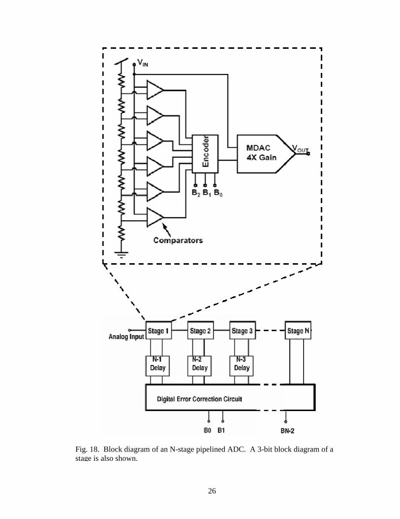
cascade of stages as shown in Fig. 18. The signal is quantized using an assembly line
25
approach where each stage quantizes a small portion of the analog signal, amplifies the
remaining signal residue, and passes it on to the next stage. Internally, a stage consists of
a low-resolution flash ADC, encoder logic, and a multiplying digital-to-analog converter
(MDAC).
The low-resolution ADC in each stage uses the flash topology; comprised of 2N-2
comparators and 2N-1 resistors, where N is the stage resolution. The resistor string
provides reference voltages for the comparators. Typically, a pipeline stage will not
quantize the top bit code (i.e. all 1’s), as this extra bit code is used to create 1-bit overlap
with the following stage. The bit overlap is used to decrease output residue by a half,
allowing extra range for digital error correction (DEC). The DEC relaxes the
requirements for the comparators, correcting any error within ±0.5 LSB of the input
reference. Each comparator compares the input voltage to a different voltage from the
reference resistor string. The comparator outputs generate a thermometer code, where the
number of comparators generating a logic 1 output value changes according to the
magnitude of the input voltage (which conceptually looks like a thermometer rising and
falling, hence the name).
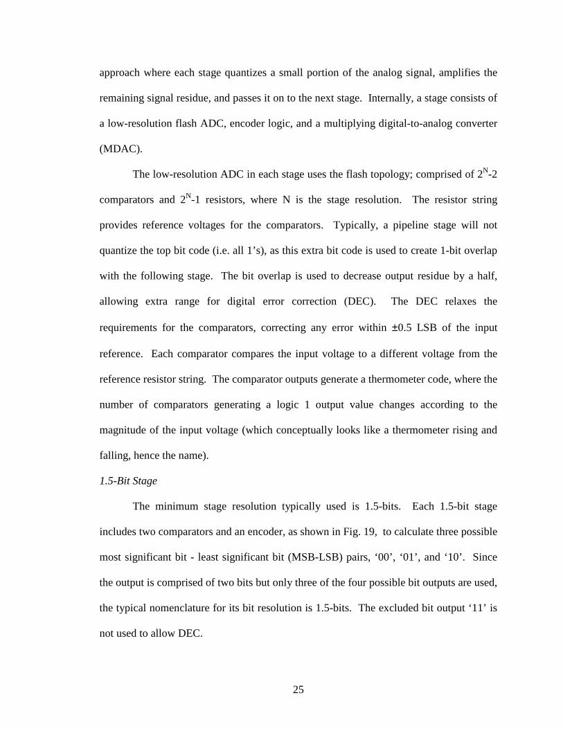
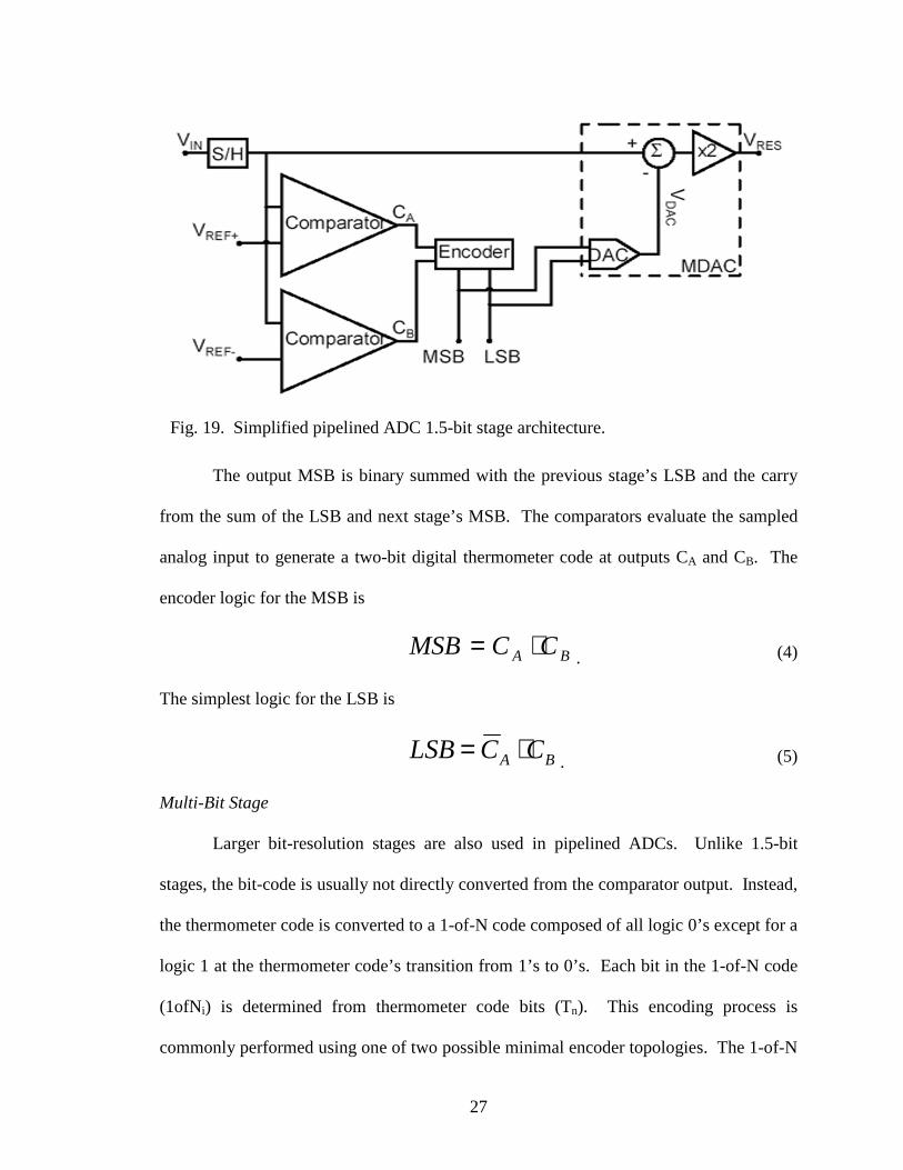
1.5-Bit Stage
The minimum stage resolution typically used is 1.5-bits. Each 1.5-bit stage
includes two comparators and an encoder, as shown in Fig. 19, to calculate three possible
most significant bit - least significant bit (MSB-LSB) pairs, ‘00’, ‘01’, and ‘10’. Since
the output is comprised of two bits but only three of the four possible bit outputs are used,
the typical nomenclature for its bit resolution is 1.5-bits. The excluded bit output ‘11’ is
not used to allow DEC.
26
Fig. 18. Block diagram of an N-stage pipelined ADC. A 3-bit block diagram of a stage is also shown.
27
The output MSB is binary summed with the previous stage’s LSB and the carry
from the sum of the LSB and next stage’s MSB. The comparators evaluate the sampled
analog input to generate a two-bit digital thermometer code at outputs CA and CB. The
encoder logic for the MSB is
BA CCMSB ⋅= . (4)
The simplest logic for the LSB is
BA CCLSB ⋅= . (5)
Multi-Bit Stage
Larger bit-resolution stages are also used in pipelined ADCs. Unlike 1.5-bit
stages, the bit-code is usually not directly converted from the comparator output. Instead,
the thermometer code is converted to a 1-of-N code composed of all logic 0’s except for a
logic 1 at the thermometer code’s transition from 1’s to 0’s. Each bit in the 1-of-N code
(1ofNi) is determined from thermometer code bits (Tn). This encoding process is
commonly performed using one of two possible minimal encoder topologies. The 1-of-N
Fig. 19. Simplified pipelined ADC 1.5-bit stage architecture.
28
code can be either determined by taking the complement of the subsequent bit with the
current and previous bits,
111 −+ ••= nnni TTTofN , (6)
or it can be determined from the complement of the next two subsequent bits with the
current bit,
nnni TTTofN ••= ++ 121 . (7)
The thermometer to 1-of-N code conversion typically uses 3-input NAND gates
to implement either (6) or (7). The 1-of-N code is then used to access the correct output
bit code from a ROM (read-only memory) table, and also selects the correct MDAC input
references.
Unlike minimum bit resolution (1.5-bit) stages, there is no unique nomenclature
for stages using DEC; it is assumed the stages overlap. For example, even though there
are 7 output codes for 3 bits, excluding the top code, a stage is not described as 2.33-bit
resolution; it is still defined as a 3-bit resolution stage.
Comparator
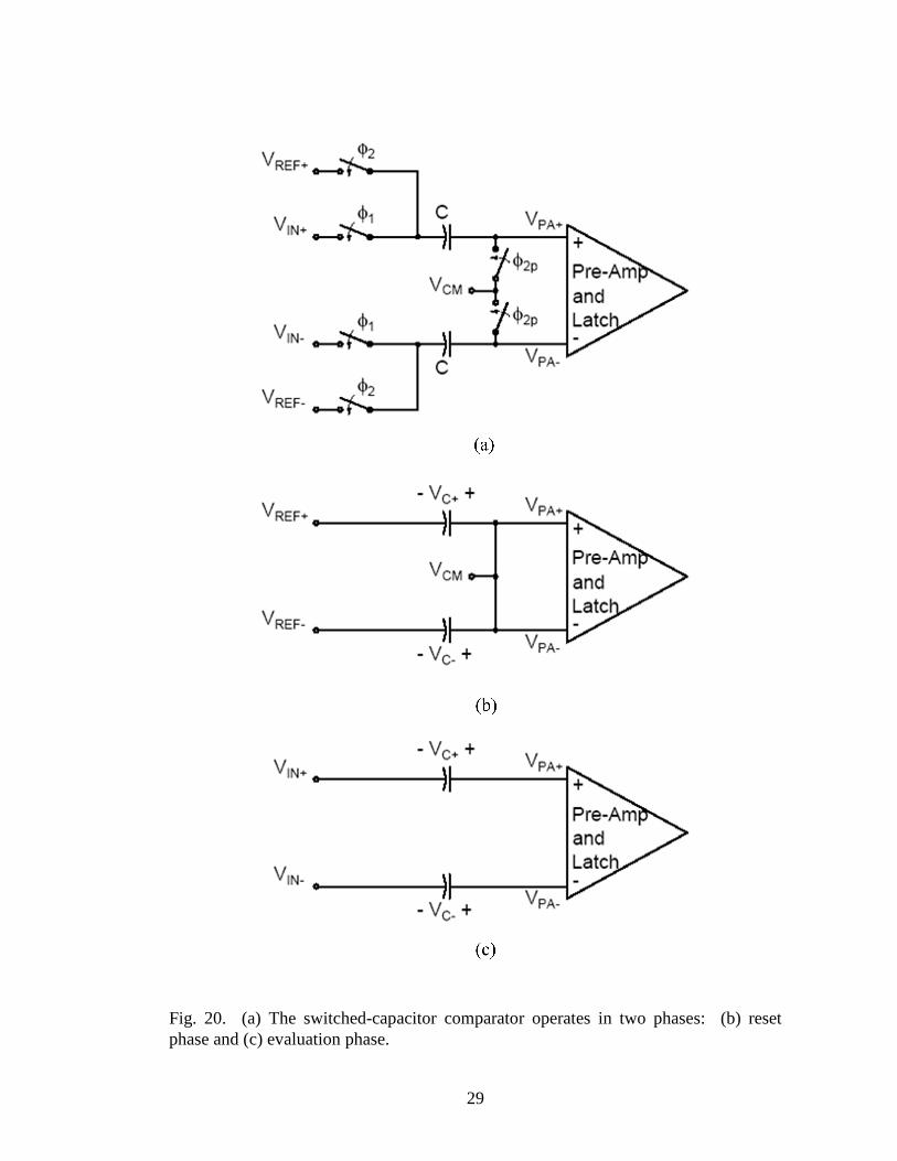
One of the important pipelined ADC sub-circuits is the comparator. Fig. 20 (a)
shows a typical switched-capacitor CMOS comparator as commonly used in pipelined
analog-to-digital converters. This comparator is composed of a capacitive input
sampling/subtraction network, a pre-amplifier, and an output latch. A reference voltage
is subtracted from the input signal, amplified, and will latch a logic ‘1’ if the difference is
positive or a logic ‘0’ if the difference is negative.
29
Fig. 20. (a) The switched-capacitor comparator operates in two phases: (b) reset phase and (c) evaluation phase.
30
The switched-capacitor comparator operates in two phases controlled by non-
overlapping clocks Φ1 and Φ2. During the reset phase, when Φ2 is high and Φ1 is low, as
shown in Fig. 20 (b), the differential reference voltage with respect to common-mode
voltage is sampled onto the capacitors,
−−
++
−=−=
REFCMC
REFCMC
VVV
VVV (8).
When Φ1 is high and Φ2 is low, as shown in Fig. 20 (c), the circuit is in evaluation
phase. The input voltage is summed with voltage stored across the capacitors from the
reset phase, resulting in the difference between input and reference voltages at the
pre-amplifier inputs,
( ) ( )−+−+−+
−−−−−
+++++
−−−=−∴−+=+=−+=+=
REFREFININPAPA
REFCMINCINPA
REFCMINCINPA
VVVVVV
VVVVVV
VVVVVV
(9).
If the differential input voltage is greater than the different reference then a logic ‘1’ will
be latched, otherwise the circuit will latch a logic ‘0’
Multiplying Digital-to-Analog Converter
Another important pipelined ADC sub-circuit is the MDAC. Once the quantizer
determines the bit-code, the MDAC generates an appropriately amplified residue voltage
as the input for the next stage in the pipeline, with each stage quantizing the next most
significant portion on the input signal. Example residue voltage transfer curves for 1 V
input range, 1.5-bit stage and 3-bit stages are shown in Figs. 21 and 22. The residue
voltage (VRES) transfer curve is a piecewise linear function with each segment having the
same slope equal to gain (G) of the MDAC. The gain is determined by 2 to power of N,
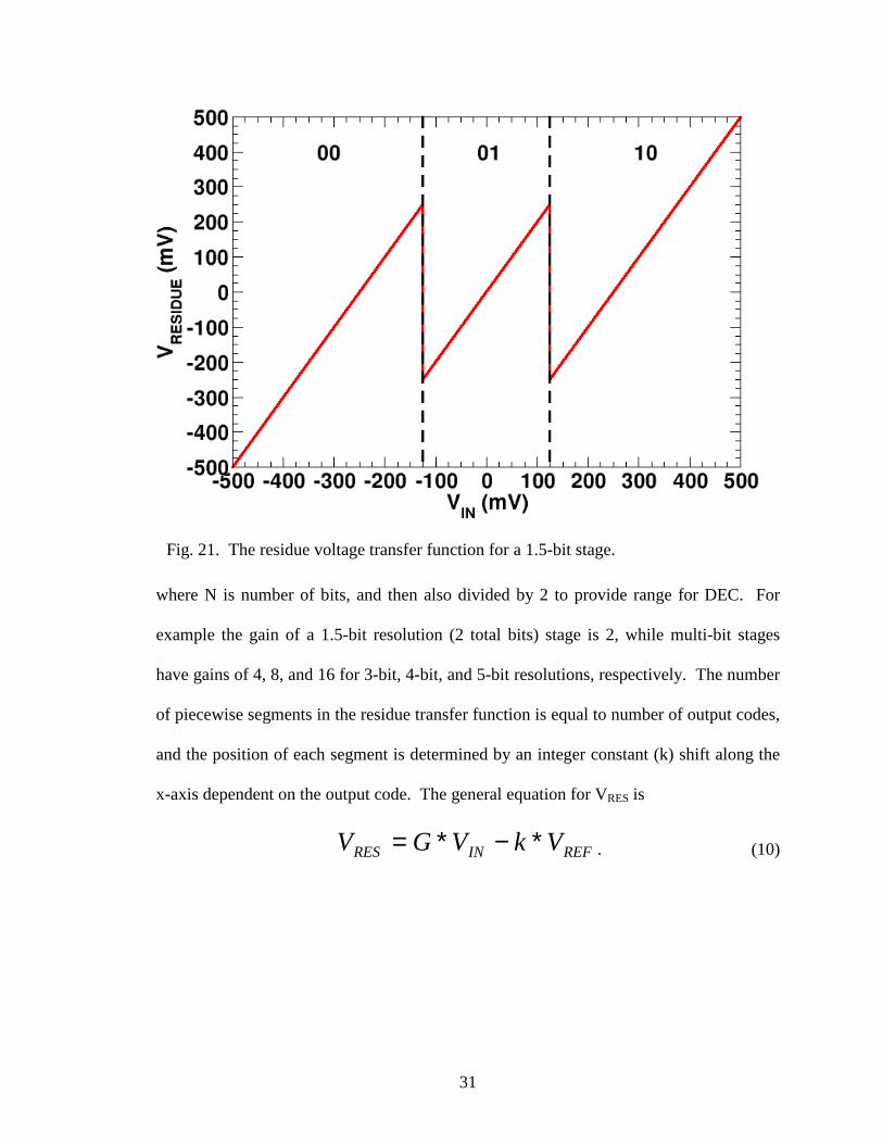
31
where N is number of bits, and then also divided by 2 to provide range for DEC. For
example the gain of a 1.5-bit resolution (2 total bits) stage is 2, while multi-bit stages
have gains of 4, 8, and 16 for 3-bit, 4-bit, and 5-bit resolutions, respectively. The number
of piecewise segments in the residue transfer function is equal to number of output codes,
and the position of each segment is determined by an integer constant (k) shift along the
x-axis dependent on the output code. The general equation for VRES is
REFINRES VkVGV ∗−∗= . (10)
Fig. 21. The residue voltage transfer function for a 1.5-bit stage.
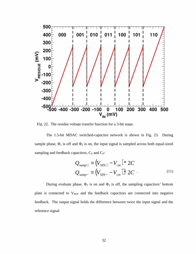
32
The 1.5-bit MDAC switched-capacitor network is shown in Fig. 23. During
sample phase, Φ1 is off and Φ2 is on, the input signal is sampled across both equal-sized
sampling and feedback capacitors, CS and CF:
( )( ) CVVQ
CVVQ
cmSINsamp
cmSINsamp
2
2
∗−=
∗−=
−−
++
. (11)
During evaluate phase, Φ1 is on and Φ2 is off, the sampling capacitors’ bottom
plate is connected to VREF and the feedback capacitors are connected into negative
feedback. The output signal holds the difference between twice the input signal and the
reference signal:
Fig. 22. The residue voltage transfer function for a 3-bit stage.

33
( )( )[ ]−+−+
−+
++−
−−+
−−
++
−−−∗∗−=−∴
+−
=
+−
=
∗−=
∗−=
REFREFSINSIN
OUTOUT
CMsevalsamp
OUT
CMsevalsamp
OUT
CMREFseval
CMREFseval
VVVV
VV
VC
QQV
VC
QQV
CVVQ
CVVQ
)(21
)(
)(
_
_
_
_
. (12)
Fig. 23. Schematic of a multiplying digital-to-analog converter switched-capacitor network used in a 1.5-bit pipelined ADC stage.
34
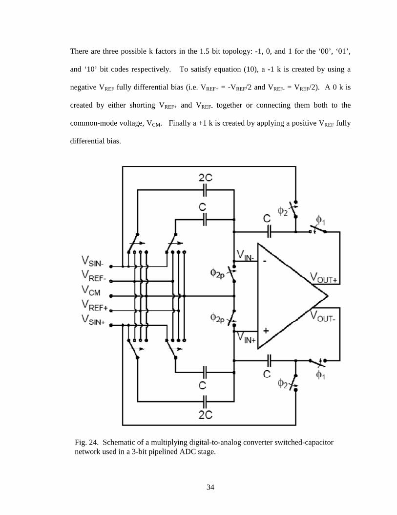
There are three possible k factors in the 1.5 bit topology: -1, 0, and 1 for the ‘00’, ‘01’,
and ‘10’ bit codes respectively. To satisfy equation (10), a -1 k is created by using a
negative VREF fully differential bias (i.e. VREF+ = -VREF/2 and VREF- = VREF/2). A 0 k is
created by either shorting VREF+ and VREF- together or connecting them both to the
common-mode voltage, VCM. Finally a +1 k is created by applying a positive VREF fully
differential bias.
Fig. 24. Schematic of a multiplying digital-to-analog converter switched-capacitor network used in a 3-bit pipelined ADC stage.
35
MDAC used in multi-bit stages are slightly different. Fig. 24 shows the fully-
differential switched-capacitor network MDAC for a 3-bit stage. A second sampling
capacitor, CS, is added in parallel and is twice the size of the original CS. Similar to the
1.5-bt MDAC, during the sampling phase all CS and CF are connected to the input signal.
During the evaluate phase the possible k factors are -3, -2, -1, 0, 1, 2, and 3 for bit codes
‘000’, ‘001’, ‘010’, ‘011’, ‘100’, ‘101’, and ‘110” respectively. The polarity of k is
achieved the same way as the 1.5-bit MDAC by the polarity of the applied VREF. The
magnitude of k is created by connecting a subset of the sampling capacitors to VREF such
that the ratio of the connected CS to CF is equal to k. The sampling capacitors not
connected to VREF are connected instead to VCM.
Conclusion
This chapter presents background on analog-to-digital circuits. The purpose of
ADCs is to discretize an analog signal to be stored and/or processed by digital circuitry.
Non-idealities in ADC performance can be measured with a variety of metrics, including
differential and integral nonlinearity and signal-to-noise ratio. The focus of this research
is on the pipelined ADC topology, since it offers a competitive balance of both high
speed and high resolution. The next chapter presents a background on single-event
phenomena in pipelined ADCs.
36
CHAPTER IV
SINGLE-EVENT EFFECTS IN PIPELINED ANALOG-TO-DIGITAL CONVERTERS
Introduction
Pipelined analog-to-digital converters (ADCs) are a preferred topology for space
and military integrated circuits because the resolution and speed performance fit a wide
range of applications. Also pipelined ADCs provide an interesting medium to study
single-events due to the complex nature of both analog and digital operation. This
chapter provides background on previous radiation testing and simulation analyses
performed on pipelined ADCs.
Heavy Ion Testing
Only a limited number of results from heavy ion irradiation of pipelined ADCs
have been published [55]-[60]. The first pipelined ADC heavy ion testing was performed
in 1994 on the 12-bit 5 MSPS AD42961, a device with 4 stages, and stage bit resolutions
of 3, 4, 4, and 4 sequentially. This ADC was designed to be radiation-hard against
neutron damage, total dose, and single-event latchup (SEL). However, the design did not
include any hardening targeted against single-event upsets or single event transients.
Errors were calculated by subtracting pre- from post-irradiation histograms of output [6].
The traditional cross-section was modified to include the dynamic sampling operation of
an ADC, changing cm2/device to cm2/MS (Mega-sample). Cross-section test results for
errors occurring in any bit, defined as raw errors, and also errors occurring only in the 7
37
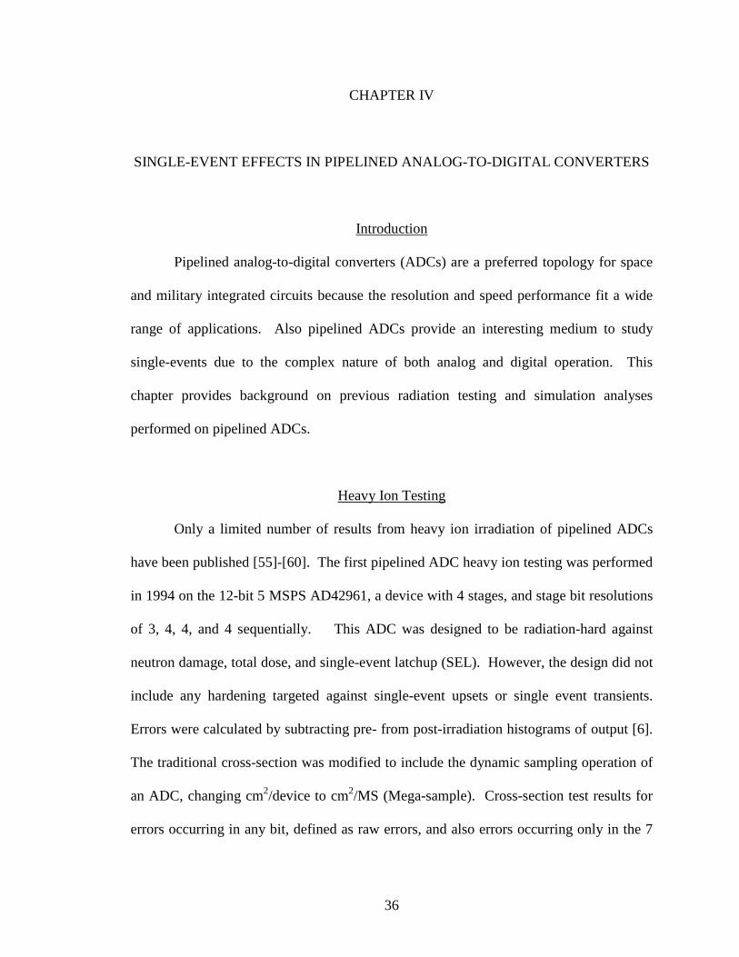
MSBs are shown in Fig 25. The saturated cross-section of errors occurring in the 7
MSBs is about 5 times smaller than the raw errors. Turflinger, et al., attributes the lack
of a strong dependence of LET on cross-section in the raw error data to charge collection
in the analog circuitry since this circuitry doesn’t have a specific critical charge [55].
Using 25% of saturated cross-section as the threshold, the errors in the 7 MSBs have a
threshold LET of 10 MeV-cm2/mg. The Turflinger, et al. paper, also estimated the error
rates for three different orbits; upsets in the 7 MSBs will occur at rates of about 3, 13, and
62 errors/day for LEO, proton belt, and GEO respectively [55].
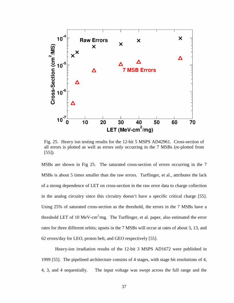
Heavy-ion irradiation results of the 12-bit 3 MSPS AD1672 were published in
1999 [55]. The pipelined architecture consists of 4 stages, with stage bit resolutions of 4,
4, 3, and 4 sequentially. The input voltage was swept across the full range and the
Fig. 25. Heavy ion testing results for the 12-bit 5 MSPS AD42961. Cross-section of all errors is plotted as well as errors only occurring in the 7 MSBs (re-plotted from [55]).
38
resulting output was compared to a non-irradiated reference device. The results are
shown in Fig. 26. The smallest tested LET, 3 MeV-cm2/mg, produced upsets in the
AD1672, but no further analysis was performed.
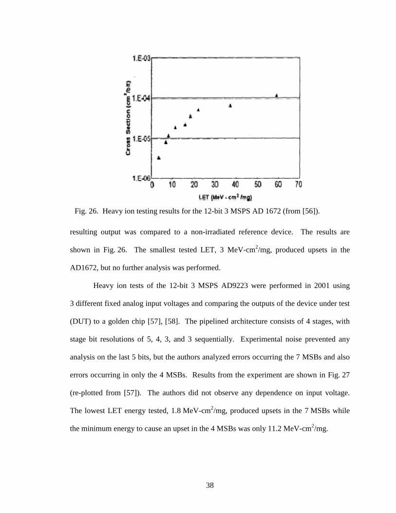
Heavy ion tests of the 12-bit 3 MSPS AD9223 were performed in 2001 using
3 different fixed analog input voltages and comparing the outputs of the device under test
(DUT) to a golden chip [57], [58]. The pipelined architecture consists of 4 stages, with
stage bit resolutions of 5, 4, 3, and 3 sequentially. Experimental noise prevented any
analysis on the last 5 bits, but the authors analyzed errors occurring the 7 MSBs and also
errors occurring in only the 4 MSBs. Results from the experiment are shown in Fig. 27
(re-plotted from [57]). The authors did not observe any dependence on input voltage.
The lowest LET energy tested, 1.8 MeV-cm2/mg, produced upsets in the 7 MSBs while
the minimum energy to cause an upset in the 4 MSBs was only 11.2 MeV-cm2/mg.
Fig. 26. Heavy ion testing results for the 12-bit 3 MSPS AD 1672 (from [56]).
39
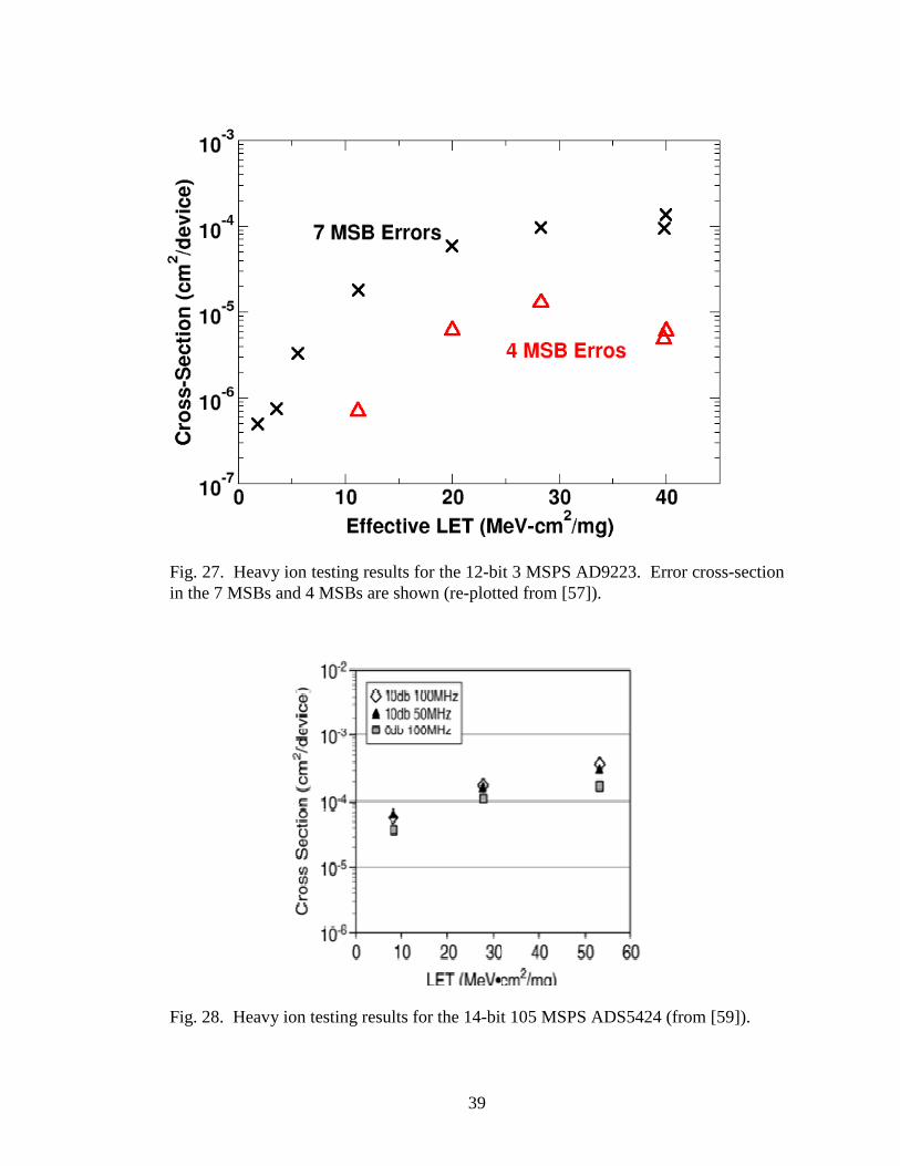
Fig. 28. Heavy ion testing results for the 14-bit 105 MSPS ADS5424 (from [59]).
Fig. 27. Heavy ion testing results for the 12-bit 3 MSPS AD9223. Error cross-section in the 7 MSBs and 4 MSBs are shown (re-plotted from [57]).
40
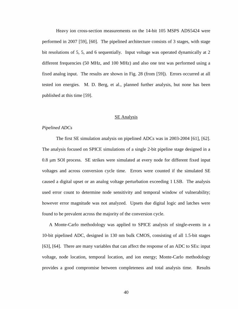
Heavy ion cross-section measurements on the 14-bit 105 MSPS ADS5424 were
performed in 2007 [59], [60]. The pipelined architecture consists of 3 stages, with stage
bit resolutions of 5, 5, and 6 sequentially. Input voltage was operated dynamically at 2
different frequencies (50 MHz, and 100 MHz) and also one test was performed using a
fixed analog input. The results are shown in Fig. 28 (from [59]). Errors occurred at all
tested ion energies. M. D. Berg, et al., planned further analysis, but none has been
published at this time [59].
SE Analysis
Pipelined ADCs
The first SE simulation analysis on pipelined ADCs was in 2003-2004 [61], [62].
The analysis focused on SPICE simulations of a single 2-bit pipeline stage designed in a
0.8 µm SOI process. SE strikes were simulated at every node for different fixed input
voltages and across conversion cycle time. Errors were counted if the simulated SE
caused a digital upset or an analog voltage perturbation exceeding 1 LSB. The analysis
used error count to determine node sensitivity and temporal window of vulnerability;
however error magnitude was not analyzed. Upsets due digital logic and latches were
found to be prevalent across the majority of the conversion cycle.
A Monte-Carlo methodology was applied to SPICE analysis of single-events in a
10-bit pipelined ADC, designed in 130 nm bulk CMOS, consisting of all 1.5-bit stages
[63], [64]. There are many variables that can affect the response of an ADC to SEs: input
voltage, node location, temporal location, and ion energy; Monte-Carlo methodology
provides a good compromise between completeness and total analysis time. Results
41
showed the most frequent errors occurred from SEs in the analog circuitry, MDAC and
sample-and-hold amplifier (SHA), however these errors were typically small in
magnitude. Large error magnitudes originate from SE strikes in the first couple stages
and occurred most frequently due to upsets in the comparators and latches. Error
resulting from comparator upsets also showed a dependence to input voltage, primarily
due to encoder logic masking and digital error correction.
Flash ADCs
The comparators and encoding circuitry in each stage of a pipelined ADC make
up a small flash ADC. Previous single-event analyses on flash ADCs will aid in the
understanding of single-events in pipelined ADCs. M. Singh, et al., used comprehensive
fault injection and nodal weighting, to analyze various ADC architectures, including a
flash ADC [65], [66]. The comparators were found to be the most sensitive sub-circuit in
the flash ADC topology. Pouget, et al., used a pulsed laser to inject charge at targeted
areas of a flash ADC [67]. In addition to using the laser to search for sensitive nodes in
the ADC, it was also synchronized to the ADC clock to investigate clock cycle
sensitivities. The largest errors came from strikes into the registers storing the MSBs
during the clock cycle after the latch operation. S. Buchner, et al., used a pulsed laser to
investigate the dependence of input voltages on overall sensitivity of a flash ADC [10],
[11]. The tests were performed because there were discrepancies between predicted error
rates and on-orbit data. During certain time periods the on-orbit data agreed with the
predicted error rates, however other time periods of on-orbit data did not match with the
predictions. The on-orbit flash ADC input code was not always the same as what was
used for the predictions. This dependence on input voltage for flash ADCs was
42
confirmed using the pulsed laser. Resulting errors would have different distributions in
magnitude and in number depending on the input voltage code and could vary as much as
an order of magnitude. It was determined that the encoding logic would sometimes mask
errors from the comparators.
SE Hardening
There are many potential sources of SE-induced errors in pipelined ADCs.
Reference, clock, and the internal sub-circuits can all be vulnerable to single-event
upsets. If one assumes that the clock circuits and reference circuits are independently
hardened, then vulnerable subcircuits within the pipeline can be hardened.
Kauppila, et al., recommended using temporally-hardened latches [61], [62];
simulations showed a significant decrease in the window of vulnerability. Sternberg,
et. al., recommended increasing the size of the sampling capacitors in the comparator and
MDAC sub-circuits and adding resistive feedback to the latches [63], [64]. E. Mikkola,
et al., showed auto-zeroing switched-capacitor architectures can limit the duration of
upset in the comparators [68]. P. Bellandi, et al., suggested using triple-modular-
redundancy (TMR) to protect the digital output registers [69].
M. Singh, et al., presented several recommendations for improving flash ADCs
[65], [66]. First, sensitivity analysis should be performed across multiple possible
sub-circuits to identify and thus implement the least sensitive sub-circuit. Pattern
detection can be used to correct or detect errors resulting from the comparators in a flash
ADC. Finally, the size of critical nodes in the comparators should be increased to
increase nodal capacitance therefore decreasing the size of injected transients.
43
Conclusion
This chapter presents background on single-events in pipelined analog-to-digital
circuits. Every experimental test shows a low threshold LET for errors and a high cross-
section, including errors in the MSBs. Unless hardening techniques are used, pipelined
ADCs will be sensitive to single-events. Previous analyses have shown large magnitude
errors can occur from SEs in latches in comparators. Comparator sensitivity to single-
events is also seen in Flash ADCs. The more abundant smaller magnitude errors are
dominated by the MDAC and S&H sub-circuits.
There is a lack of SE metrics for analyzing the contributions of both error
magnitude and frequency. Also previous SE-analyses have focused on minimum stage
resolution, even though advanced high-performance pipelined ADC design use multi-bit
stages. The current recommendations for hardening are limited; novel radiation-
hardened-by-design (RHBD) techniques are needed.
44
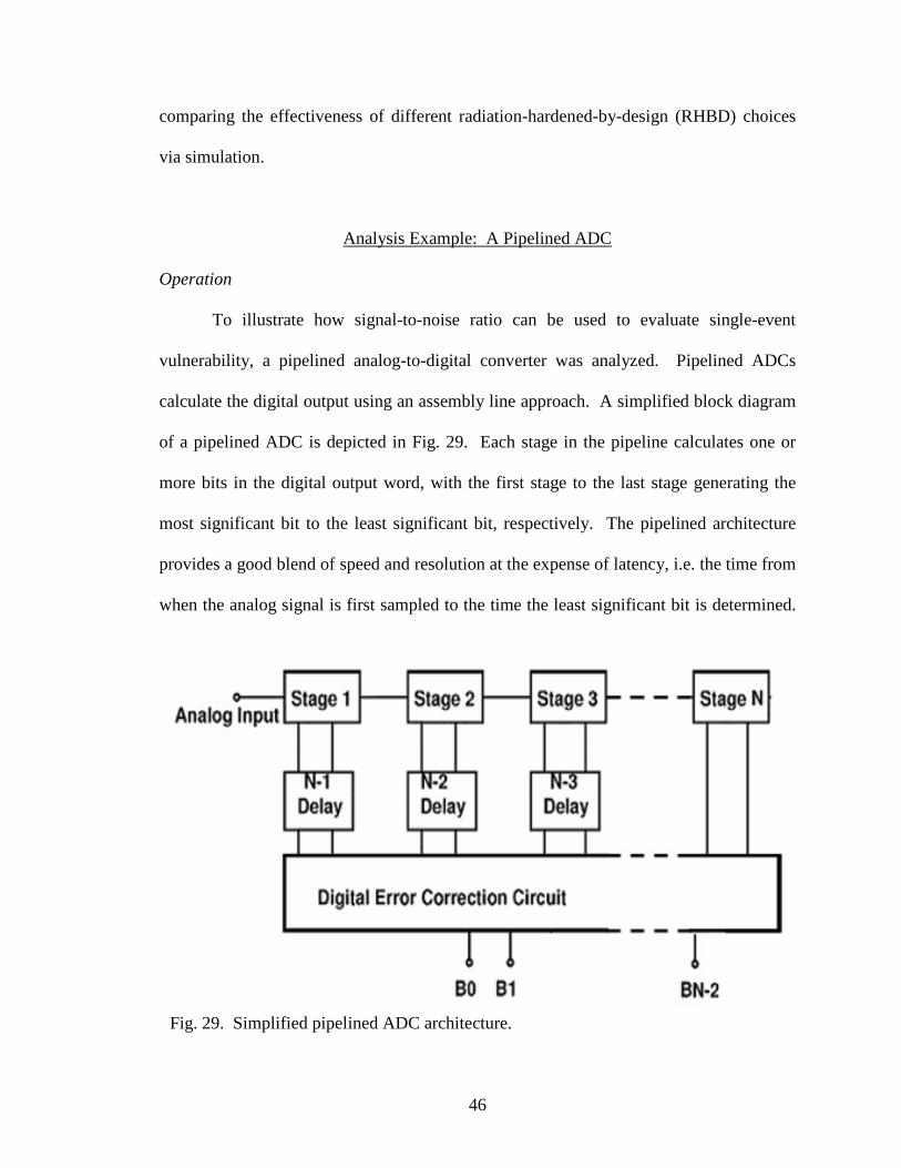
CHAPTER V
FREQUENCY DOMAIN ANALYSIS
The following chapter is a complete excerpt from a previously published
manuscript [70].
Introduction
The analysis of system-level single-event vulnerability of mixed-signal circuits
can be very challenging due to the fact that transients and upsets internal to the analog
and digital components do not necessarily appear at the system level. The extent of the
single-event response at the system level often does not correlate with the extent of
single-event response at the component level. Operating conditions may strongly affect
the overall single-event vulnerability of the system. In experimental testing of flash
analog-to-digital converters (ADCs), erroneous output data vary widely depending on the
chosen fixed input voltage for test [6], [7], [55], [71]. These factors make the single-
event analysis of mixed-signal circuits using cumulative individual responses of sub-
circuits to obtain the response of the whole system very difficult.
Even comprehensive simulations can lead to complex analysis. In one such study,
Sternberg, et al., derives cross-section curves using Monte Carlo simulations of a
pipelined ADC [63], [64]. These curves are dependent on the minimum magnitude of
error to be considered an upset, a variable that must be chosen by the designer.
Furthermore, it is difficult to evaluate and compare single event vulnerabilities when
45
different design choices for a given circuit topology lead to widely varying error
magnitude and frequency distributions. Consequently, concise SEE metrics for complex
mixed-signal circuits have been elusive. Such metrics would be particularly useful
during the design phase when determining the best techniques for mitigating single-event
errors.
Previous work has used frequency domain analysis to evaluate single events in
analog circuits [72], [73]. Furthermore, the performance of a commercial mixed-signal
circuit is often characterized in the frequency domain. One reasonable approach for an
SEE metric is to use some type of frequency domain measurement as a means of
comparing the single-event hardness of different mixed-signal circuits or systems. In an
ADC application, single-event transients can be considered as externally injected noise,
i.e. unwanted disturbances that interfere with the actual signal. Since ADCs are
inherently limited by quantization noise, their performance has long been quantified
using frequency domain metrics. Therefore, the noise added to the system by single-
event transients can be quantified using frequency domain metrics.
Parameters such as signal-to-noise ratio (SNR) and spurious free dynamic range
(SFDR) are typically used to evaluate performance in ADCs. In particular, SNR is a
parameter that is straightforward to calculate and applicable to a very wide range of
analog and mixed-signal systems. This work demonstrates a new method for comparing
the single-event hardness of different mixed-signal circuit designs. A SNR metric is
used, for the first time, to evaluate tradeoffs between single event vulnerability, area, and
power though the use of triple mode redundancy (TMR) [74] in the comparators of a
pipelined ADC. This metric enables the designer to optimize a mixed-signal circuit by
46
comparing the effectiveness of different radiation-hardened-by-design (RHBD) choices
via simulation.
Analysis Example: A Pipelined ADC
Operation
To illustrate how signal-to-noise ratio can be used to evaluate single-event
vulnerability, a pipelined analog-to-digital converter was analyzed. Pipelined ADCs
calculate the digital output using an assembly line approach. A simplified block diagram
of a pipelined ADC is depicted in Fig. 29. Each stage in the pipeline calculates one or
more bits in the digital output word, with the first stage to the last stage generating the
most significant bit to the least significant bit, respectively. The pipelined architecture
provides a good blend of speed and resolution at the expense of latency, i.e. the time from
when the analog signal is first sampled to the time the least significant bit is determined.
Fig. 29. Simplified pipelined ADC architecture.

47
However, due to the pipelined approach, the overall conversion rate of the ADC can be
quite high since new output data is available at each clock cycle.
1.5-bit Stage Design
The pipelined ADC simulated in this work has 10-bit resolution, operates at 100
Megasamples per second (MS/s), and is comprised of nine 1.5-bit stages. Each stage
includes a quantizer circuit consisting of two comparators and an encoder to calculate
three possible most significant bit-least significant bit (MSB-LSB) pairs, ‘00’, ‘01’, and
‘10’, as shown in Fig. 30. Since the output is comprised of two bits but only three of the
four possible bit outputs are used, bit resolution is defined as 1.5-bits. The excluded bit
output ‘11’ is not used in order to provide 0.5-bit overlap between stages, thereby
allowing for digital error correction (DEC).
The output bit MSB becomes part of the ADC digital output, while bit LSB is used
by the DEC circuit (not shown), except in the last stage of the pipeline. Thus, the first
eight stages of the pipeline generate eight output bits, while the last stage generates two
output bits to form the complete 10-bit output word.
Fig. 30. Simplified pipelined ADC 1.5-bit stage architecture.
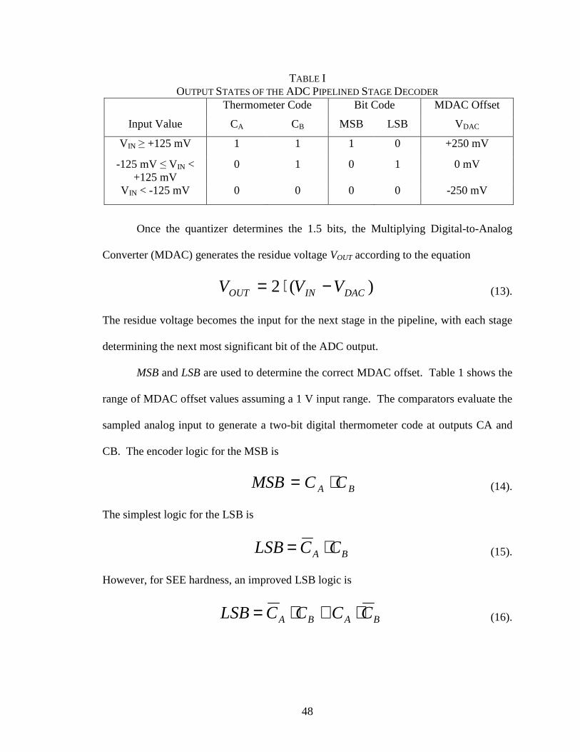
48
Once the quantizer determines the 1.5 bits, the Multiplying Digital-to-Analog
Converter (MDAC) generates the residue voltage VOUT according to the equation
)(2 DACINOUT VVV −⋅= (13).
The residue voltage becomes the input for the next stage in the pipeline, with each stage
determining the next most significant bit of the ADC output.
MSB and LSB are used to determine the correct MDAC offset. Table 1 shows the
range of MDAC offset values assuming a 1 V input range. The comparators evaluate the
sampled analog input to generate a two-bit digital thermometer code at outputs CA and
CB. The encoder logic for the MSB is
BA CCMSB ⋅= (14).
The simplest logic for the LSB is
BA CCLSB ⋅= (15).
However, for SEE hardness, an improved LSB logic is
BABA CCCCLSB ⋅+⋅= (16).
TABLE I OUTPUT STATES OF THE ADC PIPELINED STAGE DECODER
Thermometer Code Bit Code MDAC Offset
Input Value CA CB MSB LSB VDAC
V IN ≥ +125 mV 1 1 1 0 +250 mV
-125 mV ≤ VIN < +125 mV
0 1 0 1 0 mV
V IN < -125 mV 0 0 0 0 -250 mV

49
The extra encoder logic used for the LSB takes into account the invalid thermometer
code, ’10’. It ensures that if a single event forces the invalid code then the corresponding
error is no greater than the LSB of the stage.
Comparator Errors and Triple-Mode Redundancy
One source of significant errors results from single-event upsets in the
comparators. If a single event in a comparator forces its output state to flip, then the
quantizer will evaluate to an incorrect digital output. Thus, an upset in a comparator can
produce an error as large as the most significant bit for that stage. In a pipelined
converter with multiple stages, upsets occurring earlier in the pipeline will generally
create a much larger error in the digital output word and thus have a much greater effect
on SNR than upsets occurring later in the pipeline. Thus, SNR can be used to effectively
represent not only the presence of errors but also the severity of the errors at the system
level.
At this point it should be emphasized that using SNR to characterize the single-
event errors in a fabricated ADC would have little benefit unless the error rate was
extremely high. In most radiation environments, the SNR reduction due to single-event
strikes would be extremely small. With a simulator, however, the error rate can be set to
any arbitrary level, making the SNR an excellent means of evaluating different design
choices.
The application of triple-mode redundancy (TMR) to the comparators at various
stages of the pipeline was used to demonstrate the usefulness of frequency domain
analysis for evaluating system-level response of pipelined ADC circuits. TMR has
significant area and power penalties and is generally avoided unless absolutely necessary.
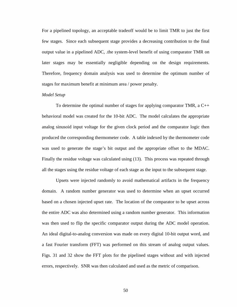
50
For a pipelined topology, an acceptable tradeoff would be to limit TMR to just the first
few stages. Since each subsequent stage provides a decreasing contribution to the final
output value in a pipelined ADC, .the system-level benefit of using comparator TMR on
later stages may be essentially negligible depending on the design requirements.
Therefore, frequency domain analysis was used to determine the optimum number of
stages for maximum benefit at minimum area / power penalty.
Model Setup
To determine the optimal number of stages for applying comparator TMR, a C++
behavioral model was created for the 10-bit ADC. The model calculates the appropriate
analog sinusoid input voltage for the given clock period and the comparator logic then
produced the corresponding thermometer code. A table indexed by the thermometer code
was used to generate the stage’s bit output and the appropriate offset to the MDAC.
Finally the residue voltage was calculated using (13). This process was repeated through
all the stages using the residue voltage of each stage as the input to the subsequent stage.
Upsets were injected randomly to avoid mathematical artifacts in the frequency
domain. A random number generator was used to determine when an upset occurred
based on a chosen injected upset rate. The location of the comparator to be upset across
the entire ADC was also determined using a random number generator. This information
was then used to flip the specific comparator output during the ADC model operation.
An ideal digital-to-analog conversion was made on every digital 10-bit output word, and
a fast Fourier transform (FFT) was performed on this stream of analog output values.
Figs. 31 and 32 show the FFT plots for the pipelined stages without and with injected
errors, respectively. SNR was then calculated and used as the metric of comparison.

51
10-bit ADC Results
The results of the using comparator TMR on a limited number of stages are
shown in Fig. 33. In this figure, SNR is plotted with respect to the number of stages in
which comparator TMR was applied. In each of these cases, comparator TMR was
applied to stages consecutively starting with the first stage, which contributes the most
significant bit in the final digital word. This figure indicates that the application of
comparator TMR to the first half of the 10-bit pipelined ADC produces the best tradeoff
in decreasing single event vulnerability versus increasing area and power. Note that the
Fig. 32. Example FFT of C++ pipelined ADC model with injected comparator upsets. A single comparator had a probability of 0.1% to upset during a sample. The simulation used 220 simulated samples.
Fig. 31. Example FFT of C++ pipelined ADC model using 220 simulated samples.
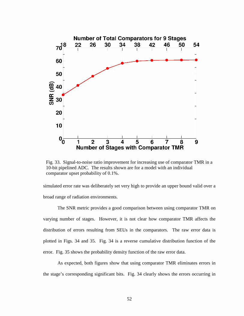
52
simulated error rate was deliberately set very high to provide an upper bound valid over a
broad range of radiation environments.
The SNR metric provides a good comparison between using comparator TMR on
varying number of stages. However, it is not clear how comparator TMR affects the
distribution of errors resulting from SEUs in the comparators. The raw error data is
plotted in Figs. 34 and 35. Fig. 34 is a reverse cumulative distribution function of the
error. Fig. 35 shows the probability density function of the raw error data.
As expected, both figures show that using comparator TMR eliminates errors in
the stage’s corresponding significant bits. Fig. 34 clearly shows the errors occurring in
Fig. 33. Signal-to-noise ratio improvement for increasing use of comparator TMR in a 10-bit pipelined ADC. The results shown are for a model with an individual comparator upset probability of 0.1%.
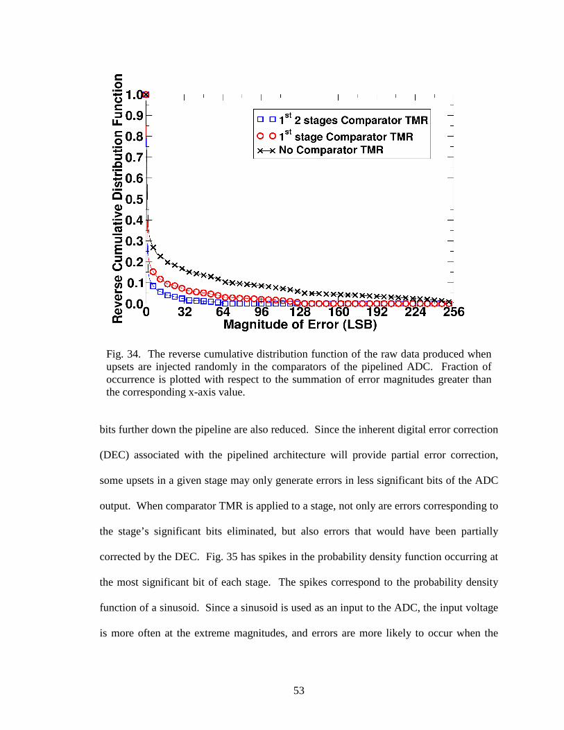
53
bits further down the pipeline are also reduced. Since the inherent digital error correction
(DEC) associated with the pipelined architecture will provide partial error correction,
some upsets in a given stage may only generate errors in less significant bits of the ADC
output. When comparator TMR is applied to a stage, not only are errors corresponding to
the stage’s significant bits eliminated, but also errors that would have been partially
corrected by the DEC. Fig. 35 has spikes in the probability density function occurring at
the most significant bit of each stage. The spikes correspond to the probability density
function of a sinusoid. Since a sinusoid is used as an input to the ADC, the input voltage
is more often at the extreme magnitudes, and errors are more likely to occur when the
Fig. 34. The reverse cumulative distribution function of the raw data produced when upsets are injected randomly in the comparators of the pipelined ADC. Fraction of occurrence is plotted with respect to the summation of error magnitudes greater than the corresponding x-axis value.
54
input is at the maximum and minimum values. Even when no comparator TMR is used,
not every comparator upset will produce an error at the output, as some will be
completely corrected by the DEC. Fig. 35 shows that full correction occurs 41% of the
time when using no comparator TMR, 58% of the time when using comparator TMR on
the 1st stage, and 70% of the time when it is used on the 1st two stages.
12-bit and 14-bit ADC Results
The results of the 10-bit ADC analysis leads to a new question: is comparator
TMR for the first four or five stages sufficient for a pipeline ADC of any resolution, or is
the optimum number of hardened stages a function of ADC resolution? To determine the
answer, the next set of simulations compared 12-bit and 14-bit ADCs. The results of
Fig. 35. The probability density function of the raw data produced when upsets are injected randomly in the comparators of the pipelined ADC.
55
these simulations are shown in Figs. 36 and 37. In all three figures (33, 36, and 37) the
SNR improvement reaches a point of diminishing return when comparator TMR is
applied to the first half of the pipeline. The apparent conclusion is that TMR is best
utilized for the same initial percentage of the pipeline regardless of resolution.
Upset Injection Rate
Finally, the effect of upset injection error rate on SNR was simulated. Fig. 38
shows the impact of the error rate on SNR. Error rate is defined as the fractional
likelihood a sample contains an injected comparator upset. As the error rate decreases,
the SNR increases at the rate of 10 dB per decade. As expected, the SNR due to single-
event errors approaches the ideal SNR at very low error rates, with the effective single-
Fig. 36. Signal-to-Noise Ratio improvement for increasing use of comparator TMR in a 12-bit pipelined ADC. The results shown are for a model with an individual comparator upset probability of 0.1%.
56
event “noise” level merging into the quantization noise floor of the ADC. Maximum
error rate simulations were performed in which an upset occurred in one of the
comparators on every data sample. Fig. 39 shows the same data as Fig. 33, plus data for
the described maximum error rate. Even though this case is obviously not realistic for
most applications, it does provide a worst-case boundary. Using this worst-case data
leads to the conclusion that a designer should apply comparator TMR only to the first
two-thirds of the pipeline at the very most. Even with extremely high SEE error rates, no
significant SNR benefit is derived by TMR hardening of the last third of the ADC
Fig. 37. Signal-to-Noise Ratio improvement for increasing use of comparator TMR in a 14-bit pipelined ADC. The results shown are for a model with an individual comparator upset probability of 0.1%.

57
pipeline. In practice, most designers may choose to limit TMR to the first half (or less)
of the pipeline, depending on the expected radiation environment.
Conclusions
Signal-to-noise ratio provides an excellent metric when comparing different single-event
mitigation design choices in an ADC. Frequency domain analysis was used to find the
point of diminishing returns for the use of TMR on the internal comparators of a
pipelined ADC. Even assuming extremely high comparator upset rates, comparator TMR
is most effective when applied to the first 50% to 70% of the total number of stages in a
1.5-bit/stage pipelined ADC, regardless of the overall resolution.
Fig. 38. The pipelined ADC signal-to-noise ratio has a power log relationship with the system error rate. The results shown are calculated from the 10-bit pipelined ADC model. Error rate is defined as the fractional likelihood a sample contains an injected comparator upset.

58
Clearly, the biggest advantage of using SNR is not to evaluate the performance of
one particular circuit, but to compare the performance of two or more different RHBD
techniques on the same circuit or system, or to compare the relative hardness of two or
more different circuit topologies. In such situations, the simulated error rate can be set
sufficiently high enough to allow the designer to make a valid comparison between
designs. Because signal-to-noise ratio is so commonly used to characterize analog and
mixed-signal systems, the SNR metric should prove equally useful in quantifying the
benefit of future RHBD techniques applied to a very broad range of designs such as
analog-to-digital converters, digital-to-analog converters, RF circuits, and analog signal
processing circuits.
Fig. 39. Comparison of comparator upset probability 0.1% and 100%. The results shown are calculated from the 10-bit pipelined ADC model.
59
CHAPTER VI
MULTI-BIT STAGES
The following chapter is a complete excerpt from a manuscript prepared for
publication.
Introduction
Analog-to-digital converters (ADCs) are essential to many space and military
applications. The pipelined ADC topology offers a good balance of speed and resolution.
This topology works by employing an assembly-line approach of quantizing a portion of
an analog signal, amplifying the un-quantized signal, and passing that signal to the next
stage.
Pipelined ADCs were originally designed with a typical stage resolution of
1.5-bits, which provides an optimal tradeoff between speed, area, and power [75].
However, thermal (kT/C) noise due to random fluctuation of charge carriers becomes a
major constraint for pipelined ADC resolutions greater than 10 bits [76]. Designs
become cumbersome when pipelined ADCs use only 1.5-bit stages, as thermal noise
forces the use of large multiplying digital-to-analog converter (MDAC) capacitors which
consume valuable area and require more power. These thermal noise requirements can
be lessened through the use of multi-bit stages, particularly at the front of the pipeline.
Some common examples of commercial pipelined ADCs using multi-bit stages are
60
Analog Devices’s AD9246, Linear Technology’s LTC2209, and National
Semiconductor’s ADC14C080.
Several papers describing methods for selecting the most optimal stage
resolutions for pipelined ADCs [75]-[79] have been published, where the number of bits
per stage is calculated according to the performance requirements of the desired ADC
application. For this paper, the most optimal configuration is not a concern, beyond the
assumption that multi-bit stages will be used in a pipelined ADC design.
Many pipelined ADCs have undergone heavy ion testing: examples include
Analog Devices’s AD42961, AD1672, and AD9223 and Texas Instrument’s ADS424
[55]-[60]. LET thresholds for these parts range from 1.8 MeV-cm2/mg to
11.2 MeV-cm2/mg. Unless SE-RHBD techniques are used, pipelined ADCs will be
sensitive to single-events.
There are many potential sources of SE-induced errors in pipelined ADCs.
Reference, clock, and the internal sub-circuits can all be vulnerable to single-event
upsets. If one assumes that the clock circuits and reference circuits are independently
hardened, then vulnerable sub-circuits within the pipeline can be hardened. Previous
research involving a comprehensive simulation analysis of 1.5-bit stages concluded that
the internal comparators and MDACs were the most sensitive sub-circuits [63] within the
pipeline stages. This work also recommended improving SE-hardness in the comparators
by increasing capacitance sizes and adding resistive feedback in the latch [63].
Several additional techniques have been developed to improve the SE-sensitivity
of the comparator sub-circuits. One technique limits the duration of upset by using an
auto-zeroing architecture for comparators [68]. Another technique reduces the
61
vulnerability of internal floating nodes in sample-and-hold and MDAC sub-circuits [80],
[81]. Triple-modular-redundancy (TMR) is recommended to protect the digital output
registers [69]. The application of TMR to the comparators in 1.5-bit stages has also been
analyzed [70].
This paper expands upon previous work in RHBD pipelined ADC design by
employing analysis and simulations to compare the differences in single-event response
of 1.5-bit stages versus multi-bit stages. The single-event error analysis focuses on the
two main sub-circuits of a pipelined ADC stage: the quantizer (comparators and encoder)
and the MDAC. An RHBD technique suitable for reducing single-event errors in multi-
bit stages is also described. This technique limits single-event bit upsets in the encoder to
a maximum of one LSB for any multi-bit stage, with only minimal layout penalty.
Background
The pipelined ADC topology consists of a cascade of stages as shown in Fig. 40.
A single stage quantizes a portion of the analog signal, amplifies the remaining signal
residue, and passes it to the next stage. A single pipeline stage consists of a low-
resolution flash ADC, an MDAC, and the corresponding encoder logic.
The flash ADC is comprised of 2N-2 comparators and 2N-1 resistors, where N is
the stage resolution. The resistor string provides reference voltages for the comparators.
Typically, a pipeline stage will not quantize the top bit code (i.e. 11...1), as this extra bit
code creates an overlap with the following stage to provide digital error correction. Each
comparator compares the input voltage to a different voltage from the reference resistor
string. The comparator outputs generate a thermometer code, where the number of

62
Fig. 40. Block diagram of an N-stage pipelined ADC. A 3-bit block diagram of a stage is also shown.
63
comparators generating a logic 1 output value changes according to the magnitude of the
input voltage (which conceptually looks like a thermometer rising and falling, hence the
name). The thermometer code is then converted to a 1-of-N code composed of all logic
0’s except for a logic 1 at the thermometer code’s transition from 1’s to 0’s. Each bit in
the 1-of-N code (1ofNi) is determined from thermometer code bits (Tn). This encoding
process is commonly performed using one of two possible minimal encoder topologies.
The 1-of-N code can be either determined by taking the complement of the subsequent bit
with the current and previous bits,
111 −+ ••= nnni TTTofN (17),
or it can be determined from the complement of the next two subsequent bits with the
current bit,
nnni TTTofN ••= ++ 121 (18).
The thermometer to 1-of-N code conversion typically uses 3-input NAND gates
to implement either (17) or (18). The 1-of-N code is then used to access the correct bit
code from a ROM (read-only memory) table, which is then used to configure the
switched-capacitor input network of an MDAC in order to correctly compute the residue
voltage for the next stage in the pipeline.
Single-Event Analysis of the Comparators
SE-Response of 3-Input NAND Encoding Schemes
Comparator metastability and component mismatch are critical design concerns
for high-speed flash ADCs, often leading to erroneous 1’s or 0’s appearing near the
64
transition point in the thermometer code. These errors are commonly referred as bubble
errors (analogous to bubbles in a mercury thermometer).
The encoding schemes described in (17) and (18) are typically used in
commercial designs because they provide adequate bubble error correction at minimal
design cost [82]. Equation (17) will produce the correct 1-of-N code for any single
erroneous 1 surrounded by 0’s. Similarly, equation (18) will produce the correct 1-of-N
code for any single erroneous 0 surrounded by 1’s. However, these encoding schemes
fail for bubbles on the opposite side of the thermometer code transition. For equation
(17), an erroneous 0 surrounded by 1’s that is two bits from the transition will produce a
incorrect 1-of-N code that is 2-bits apart from the correct 1-of-N code. Likewise, the
opposite erroneous case for equation (18) will also occur. Significantly worse are those
cases in which the bubble error (a 0 surrounded by 1’s in equation (17), or a 1 surrounded
by 0’s in equation (18)) occurs 3-bits or greater from the thermometer code transition.
These cases will produce two 1’s in the 1-of-N code, causing multiple ROM rows being
accessed and thus a wired-OR response between two output words.
Fig. 41 is an illustration of a thermometer code error causing multiple ROM rows
to be accessed. In this example, a 3-bit stage should ideally evaluate the input voltage to
a bit code of ‘010’. However, a bit flip in the thermometer code is exacerbated by two
1’s appearing in the 1-of-N code, accessing multiple ROM rows. As a result, both the
most significant bit (MSB) and the least significant bit (LSB) are flipped, erroneously
generating the top bit code which is reserved for digital error correction. While this may
not be a problem for many commercial applications, it is a concern for space and military
applications requiring applications to be single-event robust.
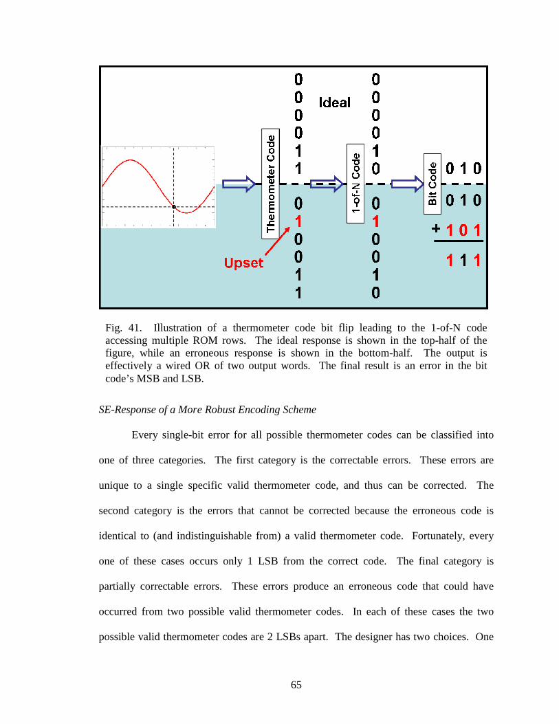
65
SE-Response of a More Robust Encoding Scheme
Every single-bit error for all possible thermometer codes can be classified into
one of three categories. The first category is the correctable errors. These errors are
unique to a single specific valid thermometer code, and thus can be corrected. The
second category is the errors that cannot be corrected because the erroneous code is
identical to (and indistinguishable from) a valid thermometer code. Fortunately, every
one of these cases occurs only 1 LSB from the correct code. The final category is
partially correctable errors. These errors produce an erroneous code that could have
occurred from two possible valid thermometer codes. In each of these cases the two
possible valid thermometer codes are 2 LSBs apart. The designer has two choices. One
Fig. 41. Illustration of a thermometer code bit flip leading to the 1-of-N code accessing multiple ROM rows. The ideal response is shown in the top-half of the figure, while an erroneous response is shown in the bottom-half. The output is effectively a wired OR of two output words. The final result is an error in the bit code’s MSB and LSB.

66
choice is to arbitrarily assign the erroneous code to one of the valid codes, leading to a
potentially correct response or to a 2 LSB error. The other option is to assign the
erroneous code to the thermometer code in between the two possible valid codes, limiting
any error to at most 1 LSB.
Previous work has investigated alternative encoder topologies in order to improve
tolerance to thermometer code errors when compared to encoders implemented using
(17) and (18). A more robust quantizing scheme was developed to protect against
metastability issues in flash ADCs [83], and later reintroduced to improve SEU tolerance
in flash ADCs [84]. However, this technique can also be applied to the encoder of a
pipelined ADC stage. This alternative encoding scheme evaluates a 1-of-N code using
the equation
( ) 1121 −++ •⊕•= nnnni TTTTofN (19).
This encoding scheme eliminates all correctable thermometer code errors. Also, for
partially correctable errors, this code assigns these those errors to the thermometer code
value between the two possible valid thermometer codes. Unlike standard 3-input
NAND logic encoders, this encoding scheme ensures that only a single ROM line will be
accessed for any single bit thermometer code upset. Most importantly, this technique
limits the maximum word error for the stage to a single LSB, regardless of the resolution
of the pipeline stage.
SE-Simulations of the 3 Different Encoding Schemes
The response of the pipelined ADC to single-event upsets originating from the
comparators was studied using a behavioral model. The model allowed effective analysis

67
of various stage design options without the need for a transistor-level design of each
circuit. A 10-bit pipelined ADC model was created in C++, which sampled a simulated
1-VP-P 24.8 MHz signal at 100 MSPS for a total of 220 samples. The ADC’s LSB is
approximately equal to 0.98 mV. Comparator upsets were injected randomly during
operation, with a probability that an individual comparator would upset at any particular
sample set to 0.1%. The relatively high probability was chosen to make comparator SEU
errors easily distinguishable from quantization error. Comparator upsets were simulated
as bit flips in the thermometer code. The ADC behavioral model was created using a
4-bit front-end stage, followed by seven 1.5-bit stages. A count of errors for both
NAND encoding schemes, shown in equations (17) and (18), and the more robust
encoding scheme shown in equation (19) are depicted in Fig. 42. Errors from ideal are
measured in multiples of the ADC’s LSB. The error distribution is not symmetric for
either of the 3-input NAND logic schemes and error magnitudes can also be quite large,
e.g. -896 LSBs for (18), and 349 LSBs for (17). This result is not surprising since upsets
can lead to multiple rows of the ROM being accessed, resulting in a convoluted ADC
error response. Single-events causing multiple ROM rows to be accessed have also been
seen with encoding logic using XOR gates [11]. The response of (19) is significantly
better. For a 1-VP-P input signal, a 1 LSB error in the 4-bit front-stage will cause a
maximum 64 LSB error in the final 10-bit ADC output. The largest errors produced by
random comparator upsets in the entire pipelined ADC correspond to a 1 LSB error in the
4-bit front-stage.
To evaluate the effectiveness of this coding scheme, it was necessary to compare
the single event response of the multi-bit stage ADC to a 1.5-bit stage ADC. In previous
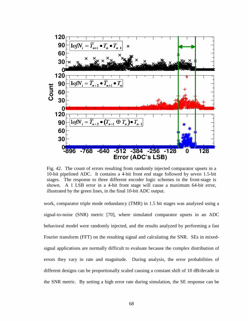
68
work, comparator triple mode redundancy (TMR) in 1.5 bit stages was analyzed using a
signal-to-noise (SNR) metric [70], where simulated comparator upsets in an ADC
behavioral model were randomly injected, and the results analyzed by performing a fast
Fourier transform (FFT) on the resulting signal and calculating the SNR. SEs in mixed-
signal applications are normally difficult to evaluate because the complex distribution of
errors they vary in rate and magnitude. During analysis, the error probabilities of
different designs can be proportionally scaled causing a constant shift of 10 dB/decade in
the SNR metric. By setting a high error rate during simulation, the SE response can be
Fig. 42. The count of errors resulting from randomly injected comparator upsets in a 10-bit pipelined ADC. It contains a 4-bit front end stage followed by seven 1.5-bit stages. The response to three different encoder logic schemes in the front-stage is shown. A 1 LSB error in a 4-bit front stage will cause a maximum 64-bit error, illustrated by the green lines, in the final 10-bit ADC output.

69
pushed above the noise floor so that comparisons between two different RHBD
techniques can be made.
The comparison of a 10-bit pipelined ADC using 1.5-bit and multi-bit stages is
shown in Fig. 43. This figure plots SNR with respect to the total number of comparators
in the entire 10-bit ADC. For the baseline case of all 1.5-bit stages, (9 stages with a total
of 18 comparators) the SNR is 34 dB. The SNR metric can be improved using
comparator TMR progressively starting with the first stage (22 total comparators) to
obtain an SNR of 41 dB, using it in the first two stages (26 total comparators) to obtain
an SNR of 48 dB, and progressing through the pipeline (adding 4 comparators per stage).
The results of using 3-, 4-, and 5-bit front-end stages are plotted in Fig. 43. Multi-
bit stages using a standard 3-input NAND logic encoder do not compare well to the
1.5-bit stages, and consequently should not be used in high radiation environments.
Since multi-bit stages have increasing number of comparators, the number of SE
vulnerable comparators in 3-input NAND logic schemes also increases, leading to a
worsening SE response with increasing resolution as shown in Fig. 43. By contrast, the
robust encoding logic scheme of (19) is far more effective against single-event upsets.
Unlike standard 3-input NAND logic encoders, where SNR worsens at higher front-end
stage bit resolutions, the robust logic encoder improves SNR by limiting the size of the
error to the LSB of the stage. For the same pipeline resolution, the 4-bit stage has nearly
the same SNR (47 dB) as three 1.5-bit stages where the first two stages utilize comparator
TMR (48 dB). Both cases have 26 total comparators, so no significant area penalty
results.
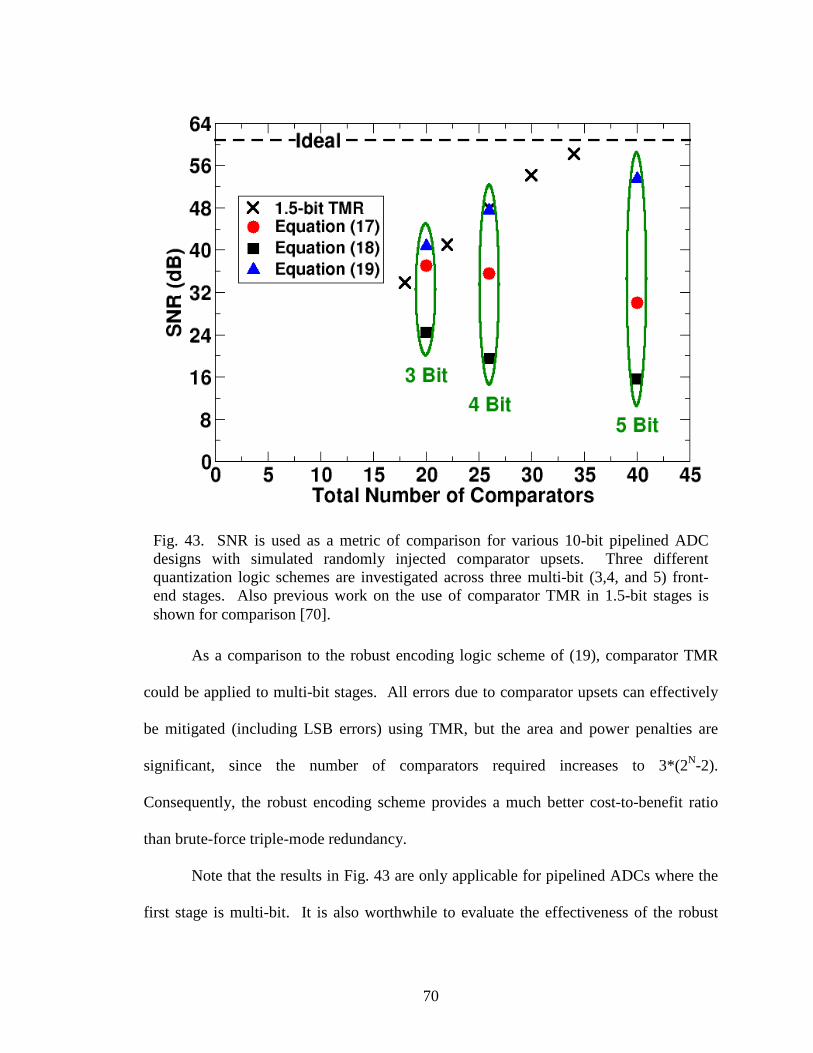
70
As a comparison to the robust encoding logic scheme of (19), comparator TMR
could be applied to multi-bit stages. All errors due to comparator upsets can effectively
be mitigated (including LSB errors) using TMR, but the area and power penalties are
significant, since the number of comparators required increases to 3*(2N-2).
Consequently, the robust encoding scheme provides a much better cost-to-benefit ratio
than brute-force triple-mode redundancy.
Note that the results in Fig. 43 are only applicable for pipelined ADCs where the
first stage is multi-bit. It is also worthwhile to evaluate the effectiveness of the robust
Fig. 43. SNR is used as a metric of comparison for various 10-bit pipelined ADC designs with simulated randomly injected comparator upsets. Three different quantization logic schemes are investigated across three multi-bit (3,4, and 5) front-end stages. Also previous work on the use of comparator TMR in 1.5-bit stages is shown for comparison [70].
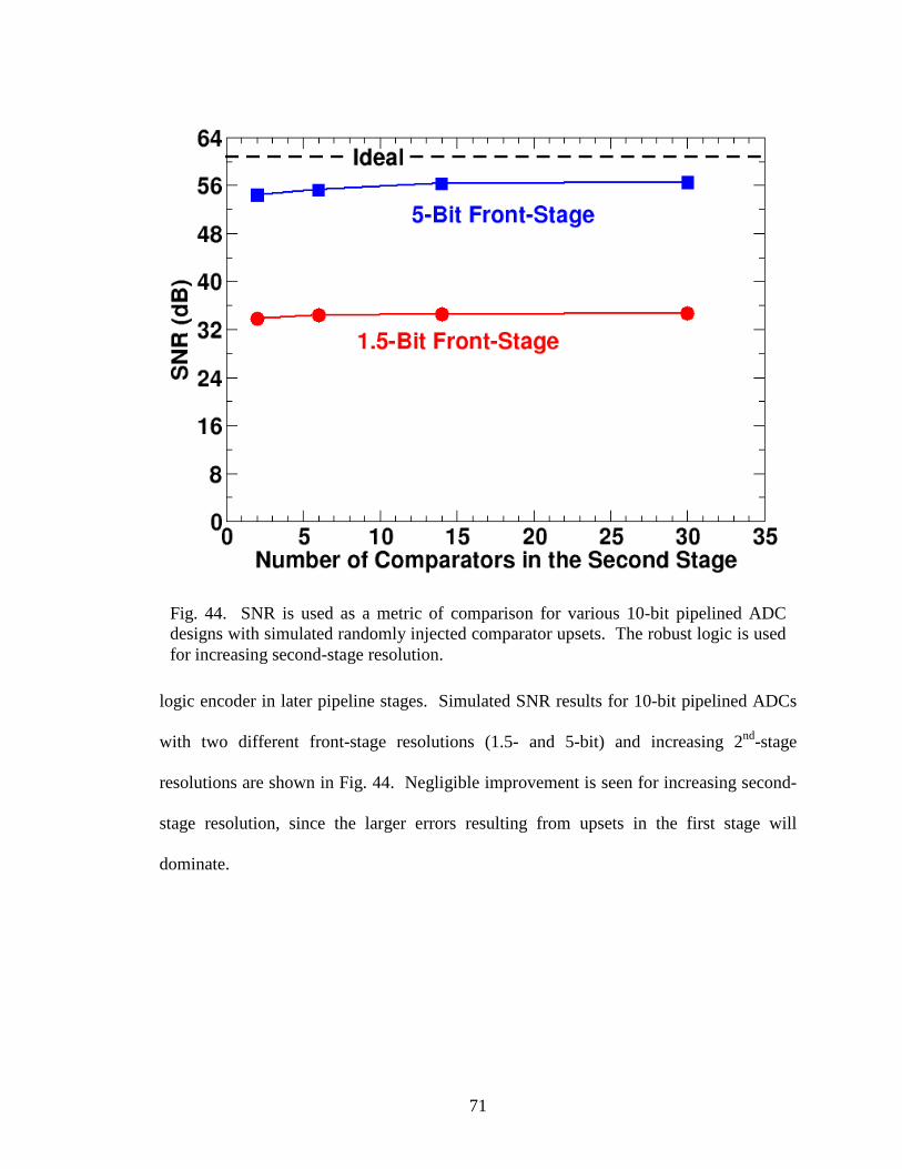
71
logic encoder in later pipeline stages. Simulated SNR results for 10-bit pipelined ADCs
with two different front-stage resolutions (1.5- and 5-bit) and increasing 2nd-stage
resolutions are shown in Fig. 44. Negligible improvement is seen for increasing second-
stage resolution, since the larger errors resulting from upsets in the first stage will
dominate.
Fig. 44. SNR is used as a metric of comparison for various 10-bit pipelined ADC designs with simulated randomly injected comparator upsets. The robust logic is used for increasing second-stage resolution.
72
Single-Event Analysis of the MDAC
SE-Response of the MDAC
Assuming the analog single-event-transient (ASET) distributions between multi-
bit MDACs and 1.5-bit MDACS are the same (to the first order), the effect of increased
per-stage resolution on the entire ADC can be better understood. First, pipelined ADCs
using multi-bit stages will have fewer MDACs, as illustrated in Fig. 45. Shown are three
1.5-bit stages, which is equivalent to a single 4 bit stage. Since every stage contains an
MDAC, the design using the 4-bit stage will have two fewer MDACs resulting in a
smaller sensitive volume. Also, because of the assembly line approach of the pipeline
topology, the error at the output of the entire pipelined ADC (∆VADC) is equal to the
ASET error at the output of the stage (∆VMDAC) is divided by the total gain (G) in the
pipeline up to that stage and can be represented by the following equation,
QVG
VkMDAC
k
i iADC ±∆•
=∆ ∏
=0
1 (20)
where Q is the quantization error of the ADC. The gain of a 1.5-bit stage is 2, while
multi-bit stages have gains of 4, 8, and 16 for 3-bit, 4-bit, and 5-bit resolutions,
respectively.
Even though an identical ASET in the MDACs of different stage resolutions will
produce a similar response at the output of the MDAC, the final ADC outputs will have
errors of different magnitudes. These errors are scaled by the gain of the stage, as shown
in equation (20). For example, the response of a 4-bit stage can be compared to the
equivalent response of three 1.5-bit stages by considering an ASET with a magnitude of
128 mV. The gain of the 4-bit stage is 8, so the equivalent output error voltage at the
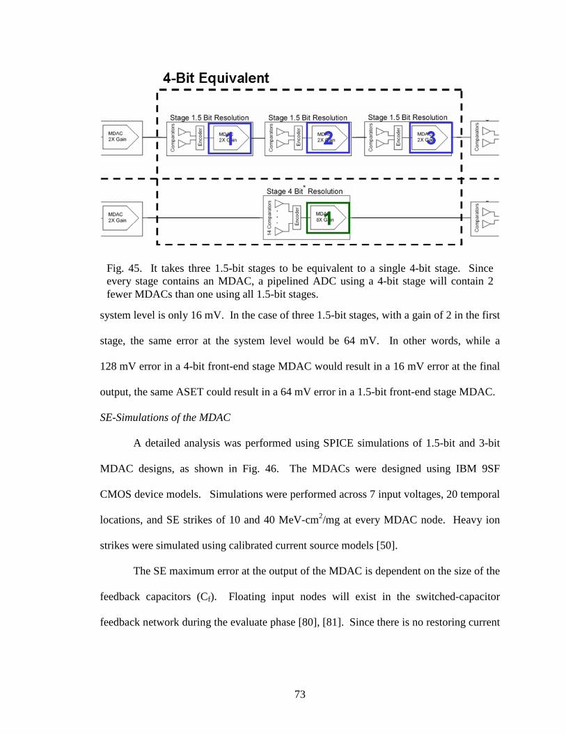
73
system level is only 16 mV. In the case of three 1.5-bit stages, with a gain of 2 in the first
stage, the same error at the system level would be 64 mV. In other words, while a
128 mV error in a 4-bit front-end stage MDAC would result in a 16 mV error at the final
output, the same ASET could result in a 64 mV error in a 1.5-bit front-end stage MDAC.
SE-Simulations of the MDAC
A detailed analysis was performed using SPICE simulations of 1.5-bit and 3-bit
MDAC designs, as shown in Fig. 46. The MDACs were designed using IBM 9SF
CMOS device models. Simulations were performed across 7 input voltages, 20 temporal
locations, and SE strikes of 10 and 40 MeV-cm2/mg at every MDAC node. Heavy ion
strikes were simulated using calibrated current source models [50].
The SE maximum error at the output of the MDAC is dependent on the size of the
feedback capacitors (Cf). Floating input nodes will exist in the switched-capacitor
feedback network during the evaluate phase [80], [81]. Since there is no restoring current
Fig. 45. It takes three 1.5-bit stages to be equivalent to a single 4-bit stage. Since every stage contains an MDAC, a pipelined ADC using a 4-bit stage will contain 2 fewer MDACs than one using all 1.5-bit stages.
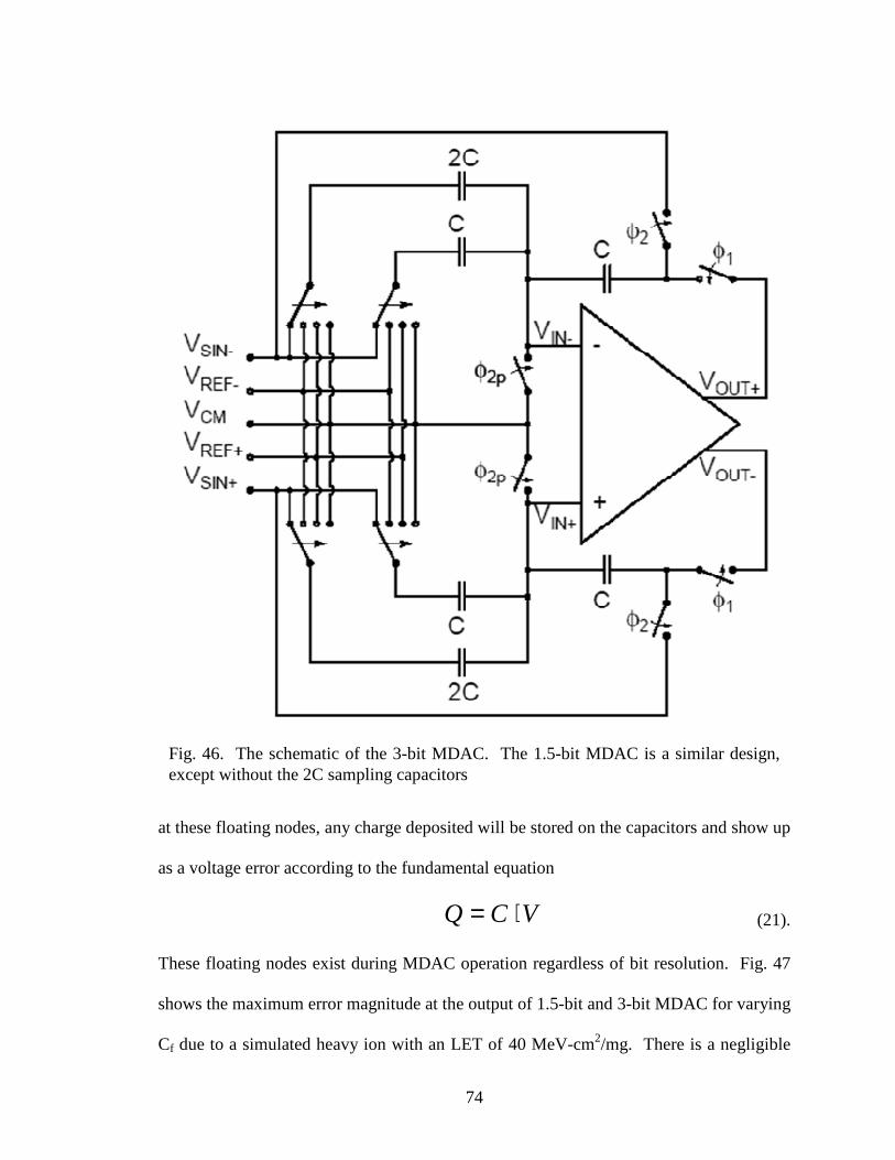
74
at these floating nodes, any charge deposited will be stored on the capacitors and show up
as a voltage error according to the fundamental equation
VCQ ⋅= (21).
These floating nodes exist during MDAC operation regardless of bit resolution. Fig. 47
shows the maximum error magnitude at the output of 1.5-bit and 3-bit MDAC for varying
Cf due to a simulated heavy ion with an LET of 40 MeV-cm2/mg. There is a negligible
Fig. 46. The schematic of the 3-bit MDAC. The 1.5-bit MDAC is a similar design, except without the 2C sampling capacitors
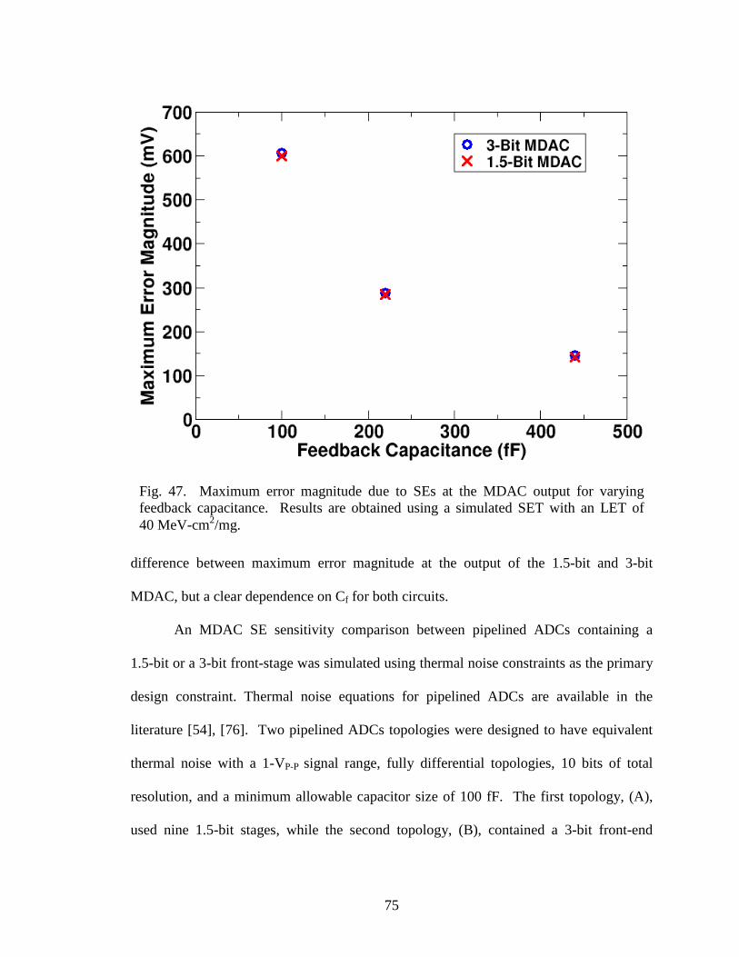
75
difference between maximum error magnitude at the output of the 1.5-bit and 3-bit
MDAC, but a clear dependence on Cf for both circuits.
An MDAC SE sensitivity comparison between pipelined ADCs containing a
1.5-bit or a 3-bit front-stage was simulated using thermal noise constraints as the primary
design constraint. Thermal noise equations for pipelined ADCs are available in the
literature [54], [76]. Two pipelined ADCs topologies were designed to have equivalent
thermal noise with a 1-VP-P signal range, fully differential topologies, 10 bits of total
resolution, and a minimum allowable capacitor size of 100 fF. The first topology, (A),
used nine 1.5-bit stages, while the second topology, (B), contained a 3-bit front-end
Fig. 47. Maximum error magnitude due to SEs at the MDAC output for varying feedback capacitance. Results are obtained using a simulated SET with an LET of 40 MeV-cm2/mg.
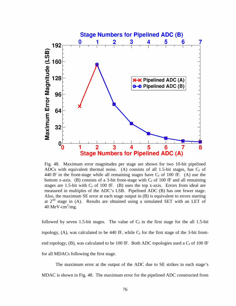
76
followed by seven 1.5-bit stages. The value of Cf in the first stage for the all 1.5-bit
topology, (A), was calculated to be 440 fF, while Cf for the first stage of the 3-bit front-
end topology, (B), was calculated to be 100 fF. Both ADC topologies used a Cf of 100 fF
for all MDACs following the first stage.
The maximum error at the output of the ADC due to SE strikes in each stage’s
MDAC is shown in Fig. 48. The maximum error for the pipelined ADC constructed from
Fig. 48. Maximum error magnitudes per stage are shown for two 10-bit pipelined ADCs with equivalent thermal noise. (A) consists of all 1.5-bit stages, has Cf of 440 fF in the front-stage while all remaining stages have Cf of 100 fF. (A) use the bottom x-axis. (B) consists of a 3-bit front-stage with Cf of 100 fF and all remaining stages are 1.5-bit with Cf of 100 fF. (B) uses the top x-axis. Errors from ideal are measured in multiples of the ADC’s LSB. Pipelined ADC (B) has one fewer stage. Also, the maximum SE error at each stage output in (B) is equivalent to errors starting at 2nd stage in (A). Results are obtained using a simulated SET with an LET of 40 MeV-cm2/mg.

77
1.5-bit stages, (A), occurred from strikes in the second stage, due to the smaller (100 fF
versus 440 fF) capacitors in the second stage. In this example, the pipelined ADC with a
3-bit front end, (B), overlaps the response of the final seven stages of (A), and will have
the same maximum MDAC error. However, the all 1.5-bit design has errors produced by
an additional stage, the first stage, and thus this circuit will have a larger sensitive area
than the pipelined ADC with a 3-bit front-end.
While the number of stages dominated the calculation of the MDAC sensitive
area, the increased number of nodes necessary to implement a multi-bit MDAC
contributes a second-order effect. For a more detailed comparison of sensitive area, each
error was weighted by the SPICE simulation node area. For simulations of SE strikes in
the MDACs with LET of 10 MeV cm2/mg, an error of at least 16 LSBs was produced in a
total area of 7.3X10⁻⁸ cm2 of the all 1.5-bit stages ADC, while the same error was
produced in a total area of only 4.8X10⁻⁸ cm2 in the ADC with a 3-bit front-end. An LET
of 40 MeV cm2/mg produced an error of at least 32 LSBs in areas of 7.7X10⁻⁸ cm2 and
5.4X10⁻⁸ cm2 in the pipelined ADCs of all 1.5-bit stages and 3-bit front-stage,
respectively.
While thermal noise constraints provide a good starting point in determining
capacitor size, it may also be necessary to increase Cf in order to meet SE sensitivity
requirements. Fig. 49 shows a decrease in maximum front-end error for increases in Cf
for SE strikes with LET of 40 MeV-cm2/mg. Increasing the front-end Cf to 220 fF
decreases the maximum MDAC error from 155 to 77 LSBs. Increasing Cf to 440 fF does
decrease the maximum error occurring in the front-stage to 37 LSBs, but 77 LSB errors
still occur from the 2nd stage. SE strikes produced an error of at least 32 LSBs in areas
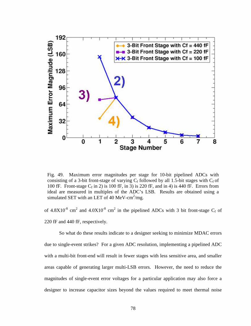
78
of 4.8X10⁻⁸ cm2 and 4.0X10⁻⁸ cm2 in the pipelined ADCs with 3 bit front-stage Cf of
220 fF and 440 fF, respectively.
So what do these results indicate to a designer seeking to minimize MDAC errors
due to single-event strikes? For a given ADC resolution, implementing a pipelined ADC
with a multi-bit front-end will result in fewer stages with less sensitive area, and smaller
areas capable of generating larger multi-LSB errors. However, the need to reduce the
magnitudes of single-event error voltages for a particular application may also force a
designer to increase capacitor sizes beyond the values required to meet thermal noise
Fig. 49. Maximum error magnitudes per stage for 10-bit pipelined ADCs with consisting of a 3-bit front-stage of varying Cf followed by all 1.5-bit stages with Cf of 100 fF. Front-stage Cf in 2) is 100 fF, in 3) is 220 fF, and in 4) is 440 fF. Errors from ideal are measured in multiples of the ADC’s LSB. Results are obtained using a simulated SET with an LET of 40 MeV-cm2/mg.
79
requirements. Consequently, the standard optimization of area versus power versus
thermal noise for pipelined ADCs as found in the literature may not be possible in an
RHBD circuit.
To summarize, if a designer does choose to implement a multi-bit front end for a
high-performance pipelined ADC, hardening that multi-bit stage against single-event
errors can be accomplished with acceptable design penalties with respect to multiple
1.5-bit stages, resulting in either equivalent or significantly reduced single-event error
magnitudes, depending on whether the MDAC or quantizer is affected.
Conclusions
The single-event sensitivity of pipelined ADCs with multi-bit stages has been
analyzed and compared to 1.5-bit stage alternatives. Multi bit stages are commonly used
in high-resolution pipelined ADC designs to provide reduced thermal noise, area, and
power. Multi-bit stages can also provide advantages with respect to single-event
vulnerability when compared to 1.5-bit stages. By utilizing a more robust encoding
scheme with little area penalty, errors resulting from comparator upsets in a multi-bit
stage can be limited to one LSB with a topology nearly as effective as 1.5-bit stages using
comparator TMR in the first pipeline stage. Pipelined ADCs with multi-bit stages will
also have fewer MDACs, leading to less sensitive area, although it may be necessary to
increase capacitor values in order to decrease SE errors resulting from strikes in the
MDACs. These results indicate that with proper design, pipelined ADCs using multi-bit
stages can be as effective as, and much more robust than, their 1.5-bit stage counterparts
when mitigating single-event errors in radiation environments.
80
CHAPTER VII
SINGLE-EVENT EFFECT MITIGATION IN SWITCHED-CAPACITOR CIRCUITS
This chapter presents novel SE-hardening techniques for switched-capacitor fully-
differential analog/mixed-signal circuits. First, a complete excerpt from a previously
published manuscript demonstrates dual-path hardening on a comparator [80]. Next, a
manuscript prepared for publication presents experimental data validating the dual-path
hardening technique in both MDAC and comparator circuits. Finally, the chapter
concludes with a discussion on analog layout techniques for SE-mitigation in fully-
differential analog/mixed-signal circuits.
Introduction to Dual-Path Hardening on a Comparator
Single-event effects in comparators have been the subject of considerable research
over the past two decades. Much of this research has focused on the analysis and
characterization of the single-event response of linear bipolar comparators. Early work
investigated the effect of heavy ions on the National Semiconductor LM111H [85]. Later
research was expanded to include various testing methodologies, testing facilities,
radiation-hardened processes, and simulation models [86]-[97]. In 2001, a radiation-
hardened-by-design linear bipolar comparator was presented that utilized triple-mode
redundancy (TMR), unique bias circuits for each comparator, and charge dissipation
techniques in the voter circuit [98]. This TMR approach was similar to that used to
harden digital circuits, with similar penalties in size, area, and power.
81
In comparison to their linear bipolar counterparts, relatively little research has
focused on single-event mitigation in CMOS comparators. In modern CMOS processes,
high-performance mixed-signal designs commonly use differential topologies and
switched-capacitor input/feedback networks to obtain greater dynamic range, better noise
rejection, improved matching, and/or reduced power dissipation relative to their single-
ended, continuous-time counterparts [99]. For example, high-speed CMOS data
converters typically make extensive use of differential switched-capacitor topologies.
Fig. 50(a) shows a typical switched-capacitor CMOS comparator as commonly
used in pipelined analog-to-digital converters. This comparator is composed of a
capacitive input sampling/subtraction network, a pre-amplifier, and an output latch.
These circuits compare an input voltage to a reference voltage and latch a logic ‘1’ or ‘0’
at the output depending on whether the input voltage is higher or lower than the
reference voltage. It is essential that valid comparator operation be ensured even in the
presence of single-events. A comprehensive SEE error analysis of the pre-amp and latch
circuits has been performed for an SOI CMOS comparator [100], but errors in the
capacitive input network were not investigated. Other work showed that an auto-zeroing
comparator design can limit upset duration to a single clock cycle between reset phases
[68], but such designs again do not address the problem of errors in the capacitive input
circuit.
In general, switched-capacitor circuit topologies exhibit much greater single-event
vulnerability than their continuous-time counterparts due to the presence of floating
nodes in the signal path [81], [101]. Floating nodes have no charge dissipation path, so
charge deposited on a floating capacitor by a single-event strike will persist until the next
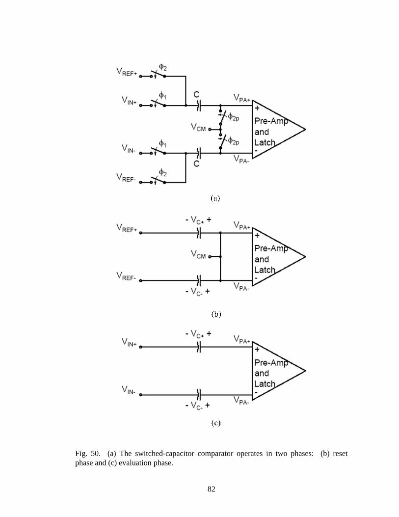
82
Fig. 50. (a) The switched-capacitor comparator operates in two phases: (b) reset phase and (c) evaluation phase.
83
clock phase. As shown in Fig. 50(c), the input network of a switched-capacitor
comparator is particularly vulnerable when its configuration results in floating input
nodes. In at least one design the input capacitor sizes were made much larger to harden
these nodes [63], but this “brute force” approach had significant penalties in terms of
layout area and maximum operating frequency.
Given sufficient time and restoring currents, a node in a continuous-time circuit
can dissipate collected charge at the cost of higher power dissipation. However,
switched-capacitor circuits have many advantages over continuous-time circuits in
precision high-speed CMOS designs, e.g. improved component matching. Consequently,
it is not practical to harden modern mixed-signal circuit designs against single-event
effects simply by migrating to continuous-time topologies, or by making capacitors
larger.
This research presents a novel solution for hardening the floating capacitive nodes
of the comparator input network, based on a modification of the “dual path” design
technique recently described for sample-and-hold feedback circuits [81]. This technique
can dramatically reduce the vulnerability of floating nodes in the switched-capacitor
input network with (at worst) a 2X capacitor area penalty. When combined with digital
error correction techniques, dual-path SEE mitigation can completely eliminate bit errors
in analog-to-digital converters due to strikes on the floating input circuits of comparators.
Circuit Operation
The switched-capacitor comparator shown in Fig. 50(a) operates in two phases
controlled by non-overlapping clocks φ1 and φ2. The switching network subtracts the
84
differential reference voltage from the differential input voltage. During the reset phase,
when φ2 is high and φ1 is low, the capacitors are precharged to the difference between the
differential reference voltage and common-mode voltage, as shown in Fig. 50(b) and
(22).
−−
++
−=−=
REFCMC
REFCMC
VVV
VVV (22)
When φ1 is high and φ2 is low, the circuit switches to the evaluation phase, and the
capacitors are connected between the input voltage and the pre-amplifier inputs. It is
during this phase that nodes connected to the input of the pre-amplifier are floating as
shown in Fig. 50(c). The differential voltage that appears at the input to the pre-amplifier
is the difference between the input signal and the reference voltages as shown by (23).
( ) ( )−+−+−+
−−−−−
+++++
−−−=−∴−+=+=−+=+=
REFREFININPAPA
REFCMINCINPA
REFCMINCINPA
VVVVVV
VVVVVV
VVVVVV
(23)
This differential input voltage is amplified and then latched as logic “1” or “0” depending
on whether the differential signal voltage or differential reference voltage is greater in
value.
Mitigation Technique
Clearly, a voltage perturbation in the differential data path of the comparator may
cause erroneous data to be latched at the comparator output. A dual signal path that
provides significant immunity to a voltage perturbation on a single floating node of a

85
switched-capacitor feedback amplifier has recently been described [81]. A modified
version of this technique can be applied to the input network of the comparator to prevent
most errors from generating an erroneous latched value. However, this dual input path
must not significantly degrade the performance of the comparator under normal
operation.
Fig. 51 shows the comparator circuit with dual inputs implemented in the
differential input stage. Input transistors M1 and M2 have each been split into two
identical transistors connected in parallel, M1A||M1B and M2A||M2B, such that the width-
to-length ratio of each parallel device is half the width-to-length ratio of the original
transistor. When the gates of M1A and M1B are shorted together, this configuration is
identical to a standard differential amplifier. However, the mitigation technique requires
Fig. 51. Simplified circuit schematic of the differential amplifier showing the split input paths.
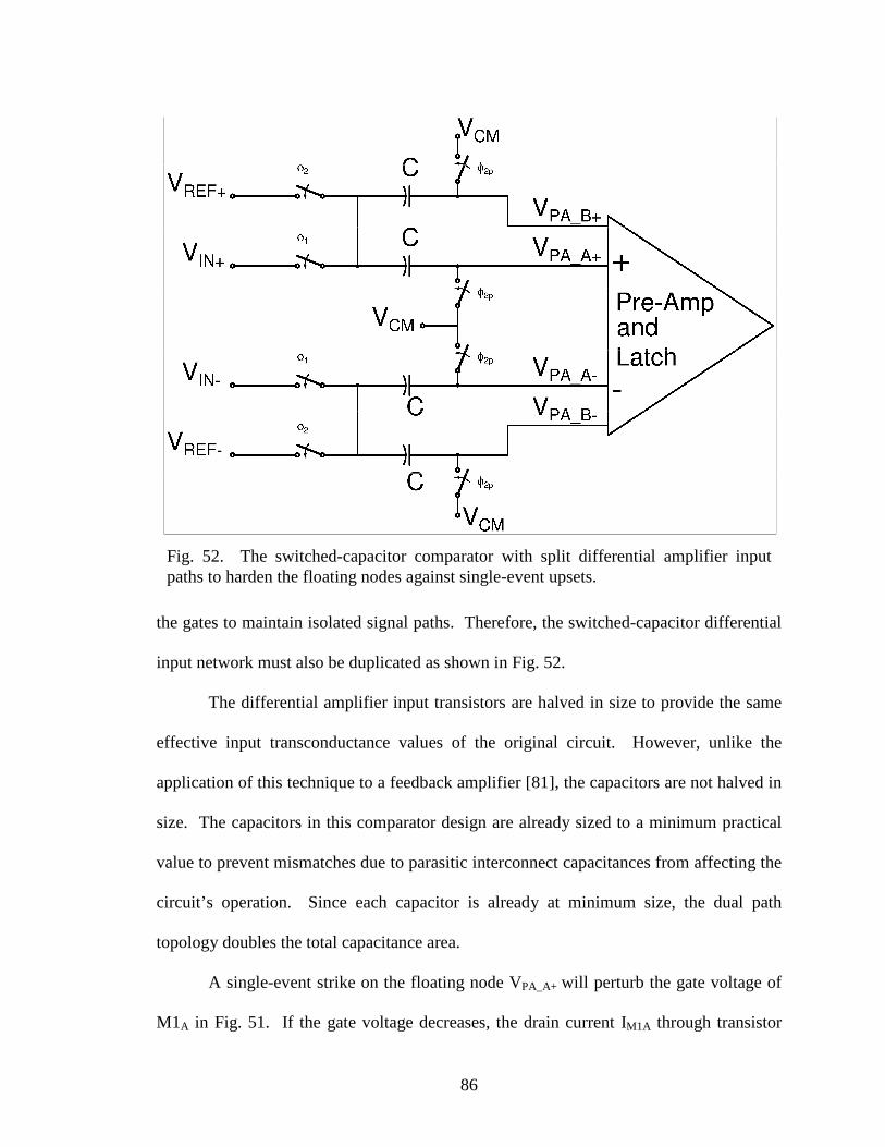
86
the gates to maintain isolated signal paths. Therefore, the switched-capacitor differential
input network must also be duplicated as shown in Fig. 52.
The differential amplifier input transistors are halved in size to provide the same
effective input transconductance values of the original circuit. However, unlike the
application of this technique to a feedback amplifier [81], the capacitors are not halved in
size. The capacitors in this comparator design are already sized to a minimum practical
value to prevent mismatches due to parasitic interconnect capacitances from affecting the
circuit’s operation. Since each capacitor is already at minimum size, the dual path
topology doubles the total capacitance area.
A single-event strike on the floating node VPA_A+ will perturb the gate voltage of
M1A in Fig. 51. If the gate voltage decreases, the drain current IM1A through transistor
Fig. 52. The switched-capacitor comparator with split differential amplifier input paths to harden the floating nodes against single-event upsets.
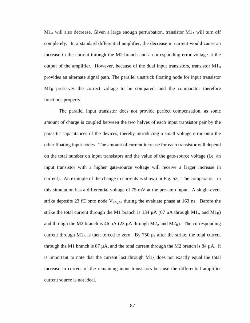
87
M1A will also decrease. Given a large enough perturbation, transistor M1A will turn off
completely. In a standard differential amplifier, the decrease in current would cause an
increase in the current through the M2 branch and a corresponding error voltage at the
output of the amplifier. However, because of the dual input transistors, transistor M1B
provides an alternate signal path. The parallel unstruck floating node for input transistor
M1B preserves the correct voltage to be compared, and the comparator therefore
functions properly.
The parallel input transistor does not provide perfect compensation, as some
amount of charge is coupled between the two halves of each input transistor pair by the
parasitic capacitances of the devices, thereby introducing a small voltage error onto the
other floating input nodes. The amount of current increase for each transistor will depend
on the total number on input transistors and the value of the gate-source voltage (i.e. an
input transistor with a higher gate-source voltage will receive a larger increase in
current). An example of the change in currents is shown in Fig. 53. The comparator in
this simulation has a differential voltage of 75 mV at the pre-amp input. A single-event
strike deposits 23 fC onto node VPA_A+ during the evaluate phase at 163 ns. Before the
strike the total current through the M1 branch is 134 µA (67 µA through M1A and M1B)
and through the M2 branch is 46 µA (23 µA through M2A and M2B). The corresponding
current through M1A is then forced to zero. By 750 ps after the strike, the total current
through the M1 branch is 87 µA, and the total current through the M2 branch is 84 µA. It
is important to note that the current lost through M1A does not exactly equal the total
increase in current of the remaining input transistors because the differential amplifier
current source is not ideal.

88
Unfortunately, this design technique cannot prevent upsets if the differential input
voltage is too small. Fig. 54 shows the dual-path RHBD technique failing for a smaller
input voltage. The SEE and comparator operating conditions were kept the same as in
Fig. 53 except the differential input voltage was decreased to 45 mV. In this case the
total current through the M1 branch after the strike remained less than the total current
through the M2 branch causing an erroneous latch.
Finally, for this mitigation technique to function effectively, a single-event strike
must turn off an input transistor rather than force it into ohmic operation. Therefore, if
the amplifier has n-type input transistors, the capacitor switches must also be n-type
Fig. 53. Currents through the differential input transistors during a single-event strike during the evaluation phase. The differential input voltage to the comparator pre-amp was 75 mV and the single-event deposited 23 fC on the floating node VPA_A+. Even though M1A is forced off, the dual path RHBD technique preserves the correct response, since the increase in current through M1B remains greater than the sum of currents through M2A and M2B. The comparator will latch the correct logic state.
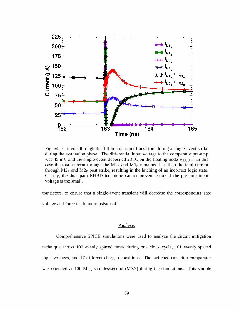
89
transistors, to ensure that a single-event transient will decrease the corresponding gate
voltage and force the input transistor off.
Analysis
Comprehensive SPICE simulations were used to analyze the circuit mitigation
technique across 100 evenly spaced times during one clock cycle, 101 evenly spaced
input voltages, and 17 different charge depositions. The switched-capacitor comparator
was operated at 100 Megasamples/second (MS/s) during the simulations. This sample
Fig. 54. Currents through the differential input transistors during a single-event strike during the evaluation phase. The differential input voltage to the comparator pre-amp was 45 mV and the single-event deposited 23 fC on the floating node VPA_A+. In this case the total current through the M1A and M1B remained less than the total current through M2A and M2B post strike, resulting in the latching of an incorrect logic state. Clearly, the dual path RHBD technique cannot prevent errors if the pre-amp input voltage is too small.
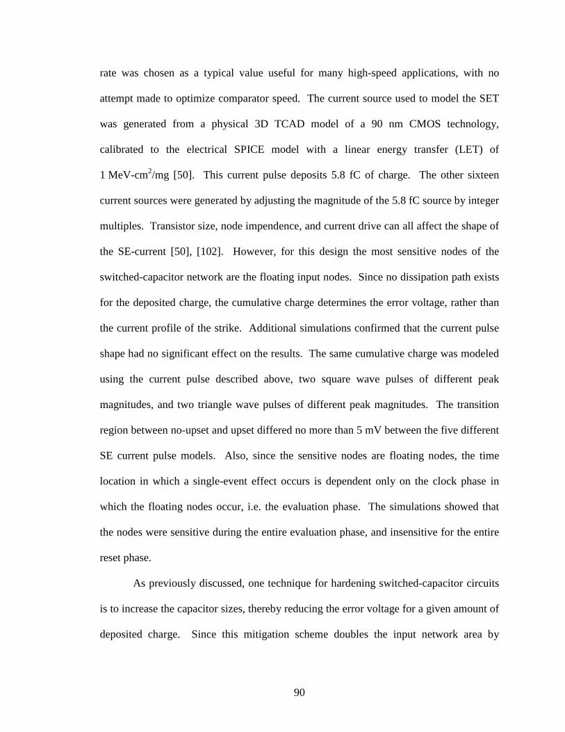
90
rate was chosen as a typical value useful for many high-speed applications, with no
attempt made to optimize comparator speed. The current source used to model the SET
was generated from a physical 3D TCAD model of a 90 nm CMOS technology,
calibrated to the electrical SPICE model with a linear energy transfer (LET) of
1 MeV-cm2/mg [50]. This current pulse deposits 5.8 fC of charge. The other sixteen
current sources were generated by adjusting the magnitude of the 5.8 fC source by integer
multiples. Transistor size, node impendence, and current drive can all affect the shape of
the SE-current [50], [102]. However, for this design the most sensitive nodes of the
switched-capacitor network are the floating input nodes. Since no dissipation path exists
for the deposited charge, the cumulative charge determines the error voltage, rather than
the current profile of the strike. Additional simulations confirmed that the current pulse
shape had no significant effect on the results. The same cumulative charge was modeled
using the current pulse described above, two square wave pulses of different peak
magnitudes, and two triangle wave pulses of different peak magnitudes. The transition
region between no-upset and upset differed no more than 5 mV between the five different
SE current pulse models. Also, since the sensitive nodes are floating nodes, the time
location in which a single-event effect occurs is dependent only on the clock phase in
which the floating nodes occur, i.e. the evaluation phase. The simulations showed that
the nodes were sensitive during the entire evaluation phase, and insensitive for the entire
reset phase.
As previously discussed, one technique for hardening switched-capacitor circuits
is to increase the capacitor sizes, thereby reducing the error voltage for a given amount of
deposited charge. Since this mitigation scheme doubles the input network area by

91
doubling the number of capacitors, an obvious question to be answered is if the increased
hardness of the comparator is simply due to the larger capacitor area, or if the dual input
path topology truly provides additional benefit. Consequently, as a “sanity check” the
dual-input comparator design was also compared to a standard switched-capacitor design
with each capacitor doubled in size.
Discussion
Results of the Dual Path RHBD Topology
Splitting the differential inputs to the comparator provides a dramatic
improvement in single-event hardness as seen by the contour plots of Fig. 55. The
differential input voltage is shown on the x-axis while the deposited charge is shown on
the y-axis. The dark region indicates an upset condition versus the light region indicating
no upset. For the standard circuit topologies of Figs. 55(a) and 55(b), the susceptible
input voltage region increases with deposited charge according to the fundamental
capacitor equation V = Q/C. This increase is not strictly linear, as higher deposited
charges eventually create a dissipation path by forcing the floating node to become so
negative that the switching transistor connected to the node turns on.
The single-event-hardened dual-path topology does not follow this semi-linear
relationship. In fact, the upset-susceptible input voltage region in Fig. 55(c) quickly
saturates. This saturation occurs because the struck node (e.g. node VPA_A+) quickly turns
off the amplifier’s input transistor (M1A), and additional deposited charge cannot turn it
“more” off. The results in Fig. 55(c) show upsets can still occur when the magnitude of
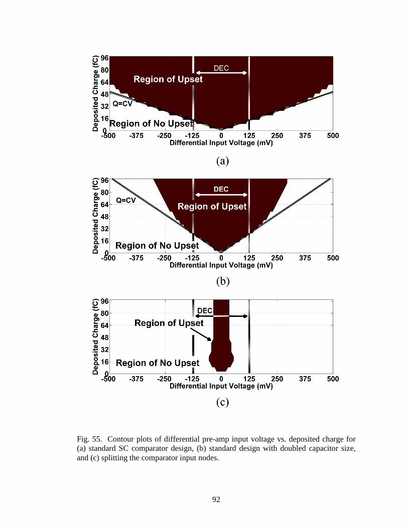
92
Fig. 55. Contour plots of differential pre-amp input voltage vs. deposited charge for (a) standard SC comparator design, (b) standard design with doubled capacitor size, and (c) splitting the comparator input nodes.
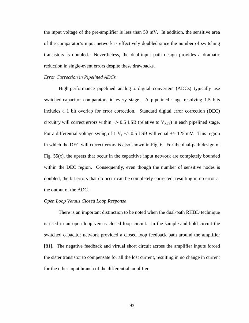
93
the input voltage of the pre-amplifier is less than 50 mV. In addition, the sensitive area
of the comparator’s input network is effectively doubled since the number of switching
transistors is doubled. Nevertheless, the dual-input path design provides a dramatic
reduction in single-event errors despite these drawbacks.
Error Correction in Pipelined ADCs
High-performance pipelined analog-to-digital converters (ADCs) typically use
switched-capacitor comparators in every stage. A pipelined stage resolving 1.5 bits
includes a 1 bit overlap for error correction. Standard digital error correction (DEC)
circuitry will correct errors within +/- 0.5 LSB (relative to VREF) in each pipelined stage.
For a differential voltage swing of 1 V, +/- 0.5 LSB will equal +/- 125 mV. This region
in which the DEC will correct errors is also shown in Fig. 6. For the dual-path design of
Fig. 55(c), the upsets that occur in the capacitive input network are completely bounded
within the DEC region. Consequently, even though the number of sensitive nodes is
doubled, the bit errors that do occur can be completely corrected, resulting in no error at
the output of the ADC.
Open Loop Versus Closed Loop Response
There is an important distinction to be noted when the dual-path RHBD technique
is used in an open loop versus closed loop circuit. In the sample-and-hold circuit the
switched capacitor network provided a closed loop feedback path around the amplifier
[81]. The negative feedback and virtual short circuit across the amplifier inputs forced
the sister transistor to compensate for all the lost current, resulting in no change in current
for the other input branch of the differential amplifier.

94
Circuits with open loop amplifier topologies, such as the comparator, behave
somewhat differently. If an input transistor is forced off by a single-event strike,
capacitive coupling will force a voltage change on all of the floating input nodes of the
comparator. Instead of the lost current being compensated for by only the sister
transistor, the current is distributed across all the input transistors. If the differential input
voltage is small enough, the dual input path topology may still fail, as the case in Fig. 54.
As shown in Fig. 55(c), errors can still occur if the differential input voltage to the pre-
amplifier is 50 mV or less.
The effectiveness of the technique for open loop circuits can be further improved
by increasing the number of input paths. There are two reasons why adding more input
transistors will improve the single-event hardness of the switched-capacitor floating
nodes. First, the percentage of current lost from the total branch current will be reduced.
The maximum current loss in the dual-path design is one half of the total branch current,
since at most one of the two dual input paths can be turned off. By switching to a quad-
path design the maximum current loss would decrease to one quarter of the total branch
current. The second reason is due to the way the lost current is redistributed. The
redistribution of lost current will depend on the total number on input transistors and the
gate-source voltages. In the worst case of the dual-path design, only three of the four
input transistors will be operational during a single-event strike. This means the branch
being affected by the single event will contain only one of the total three transistors
receiving the lost current redistribution. For the quad-path design this improves to three
of the total seven operational transistors. Since the lost current is distributed across all
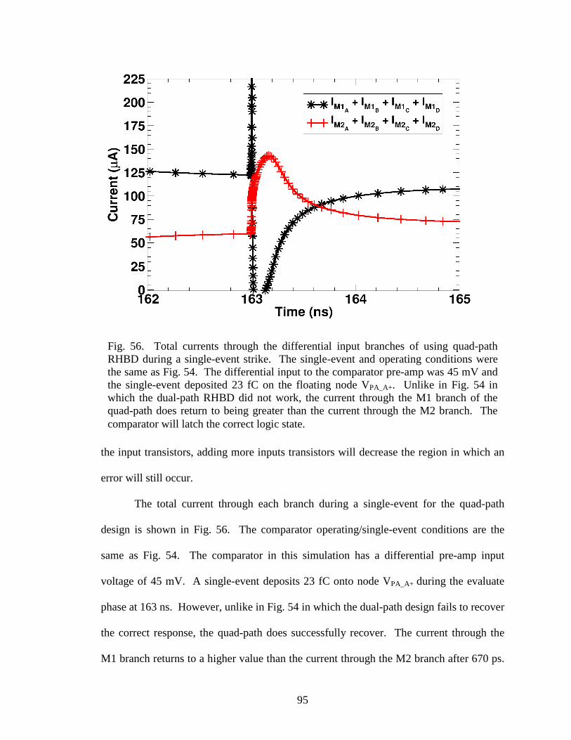
95
the input transistors, adding more inputs transistors will decrease the region in which an
error will still occur.
The total current through each branch during a single-event for the quad-path
design is shown in Fig. 56. The comparator operating/single-event conditions are the
same as Fig. 54. The comparator in this simulation has a differential pre-amp input
voltage of 45 mV. A single-event deposits 23 fC onto node VPA_A+ during the evaluate
phase at 163 ns. However, unlike in Fig. 54 in which the dual-path design fails to recover
the correct response, the quad-path does successfully recover. The current through the
M1 branch returns to a higher value than the current through the M2 branch after 670 ps.
Fig. 56. Total currents through the differential input branches of using quad-path RHBD during a single-event strike. The single-event and operating conditions were the same as Fig. 54. The differential input to the comparator pre-amp was 45 mV and the single-event deposited 23 fC on the floating node VPA_A+. Unlike in Fig. 54 in which the dual-path RHBD did not work, the current through the M1 branch of the quad-path does return to being greater than the current through the M2 branch. The comparator will latch the correct logic state.
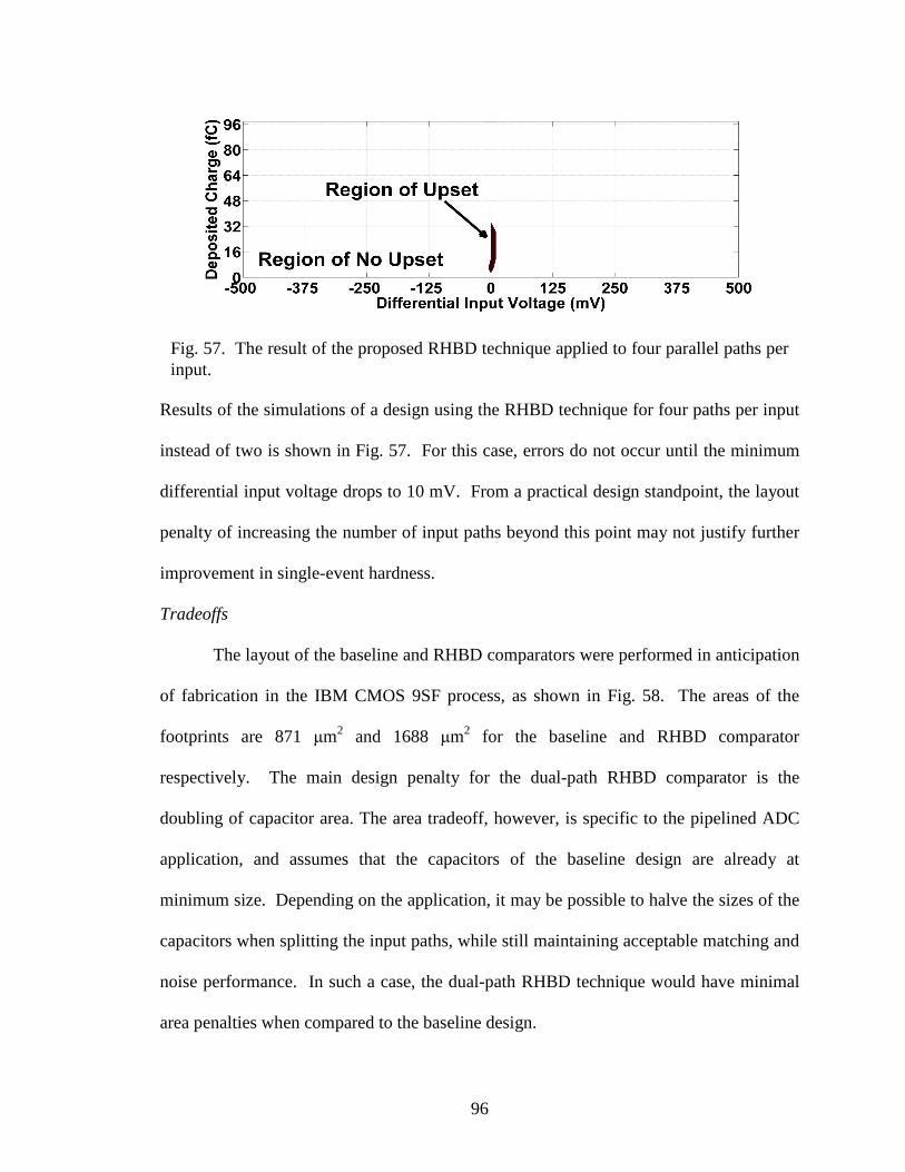
96
Results of the simulations of a design using the RHBD technique for four paths per input
instead of two is shown in Fig. 57. For this case, errors do not occur until the minimum
differential input voltage drops to 10 mV. From a practical design standpoint, the layout
penalty of increasing the number of input paths beyond this point may not justify further
improvement in single-event hardness.
Tradeoffs
The layout of the baseline and RHBD comparators were performed in anticipation
of fabrication in the IBM CMOS 9SF process, as shown in Fig. 58. The areas of the
footprints are 871 µm2 and 1688 µm2 for the baseline and RHBD comparator
respectively. The main design penalty for the dual-path RHBD comparator is the
doubling of capacitor area. The area tradeoff, however, is specific to the pipelined ADC
application, and assumes that the capacitors of the baseline design are already at
minimum size. Depending on the application, it may be possible to halve the sizes of the
capacitors when splitting the input paths, while still maintaining acceptable matching and
noise performance. In such a case, the dual-path RHBD technique would have minimal
area penalties when compared to the baseline design.
Fig. 57. The result of the proposed RHBD technique applied to four parallel paths per input.
97
Fig. 58. The completed layout designs for (a) baseline and (b) RHBD comparator. The process used is the IBM CMOS 9SF.
98
Speed penalties are dependent on the application. If the capacitors can be halved
in size, then the total capacitance for the circuit will not change, and the dual-path design
will have no significant speed penalties. However, the capacitors were kept the same size
in the ADC comparator application, and by implementing the dual-path design the total
capacitance of the system doubled. As long as the switches driving the capacitors are
replicated in each path, or their width-to-length ratios are doubled, the RC time constants
will not increase. Speed penalties will also depend on the circuits driving the VIN, VREF,
and VCM inputs. If these circuits are slew-rate limited then maximum sampling speed
will at worst be halved. However, if these circuits are not slew-rate limited then there is
no speed penalty.
The dual-path topology has negligible power penalties. There is effectively no
increase in power in the pre-amp and latch subcomponents. Even though the dual-path
RHBD technique doubles the number of input transistors, the width-to-length ratios are
halved, with no resulting changes in current. Although the number of capacitors is
doubled and the number of switches is increased, any increase in power in the switched-
capacitor subtraction network is negligible when compared to the power dissipation of
the pre-amp and latch. Simulation of a sinusoid input to both baseline and RHBD
comparators shows an average power of 101 µW for both designs.
Transistor and capacitor mismatch are also of concern in analog differential
topologies. Switched-capacitor topologies provide greater precision than continuous-
time circuits, since it is easier to match capacitors than resistors. However, if an input
transistor is forced off in a dual-path circuit, the result is an effective 1:2 mismatch
between the differential inputs, resulting in an input offset voltage. (For a quad-path
99
design the mismatch ratio will be 3:4). While many switched-capacitor circuit designs
can correct for offset errors caused by mismatches [51], [68], [99], [103]-[105], the
digital error correction in a pipelined ADC significantly reduces the matching
requirements of the comparators by correcting any offset voltage errors up to one-half of
an LSB. Conceptually it can be seen in Fig. 6 and Fig. 8 that any input offset voltage
induced by an input transistor being shut off must fall within the ± 50 mV and ± 10 mV
upset ranges in the simulations, and therefore be well within the ± 0.5 LSB correction
range of the DEC circuitry of the pipelined ADC.
Conclusions to Dual-Path Hardening on a Comparator
The dual-path RHBD technique provides a simple but effective means of
hardening the floating input nodes for a switched-capacitor comparator. By splitting the
input nodes into separate parallel signal paths, a dramatic improvement in single-event
hardness is observed. For a pipelined ADC, the input voltage region over which the
comparator does upset can be completely bounded by digital error correction, effectively
eliminating all bit errors due to the single-event strikes on the input networks of the
comparators. These results indicate that the dual-path RHBD technique should be
extremely effective at reducing single-event errors for a broad range of switched-
capacitor circuits, with or without feedback.
The tradeoff for using the dual-path technique is increased layout complexity, an
increase in the number of switching transistor, and a doubling of overall capacitor area,
assuming that the input capacitors were originally at minimum size. However,
100
simulations show that the effectiveness of this hardening scheme easily justifies this
design penalty for high-performance mixed-signal applications.
Introduction to Dual-Path Hardening Experimental Validation
In modern CMOS processes, high-performance mixed-signal designs commonly
use differential topologies and switched-capacitor input/feedback networks to obtain
greater dynamic range, better noise rejection, improved matching, and/or reduced power
dissipation relative to their single-ended, continuous-time counterparts [99]. In general,
switched-capacitor circuit topologies exhibit much greater single-event vulnerability than
the continuous-time analogs due to the presence of floating nodes in the signal path [81].
Floating nodes have no charge dissipation path, so charge deposited on a floating
capacitor by a single-event strike will persist until the next clock phase.
Previous work in hardening switched-capacitor circuits involves increasing the
size of the inputs capacitors [63]. This “brute force” approach has significant penalties in
terms of layout area and maximum operating frequency. Similarly, given sufficient time
and restoring currents, a node in a continuous-time circuit can dissipate collected charge
at the cost of higher power dissipation. The circuit-performance advantages of switched-
capacitor topologies outweigh the complications of hardening these circuits for single-
event effects. The drawbacks of these techniques make it impractical to harden modern
mixed-signal circuit designs against single-event effects simply by migrating to
continuous-time topologies, or by making capacitors larger.
This research presents experimental results for hardening the floating capacitive
nodes of switched-capacitor circuits, based on using the dual-path hardening technique
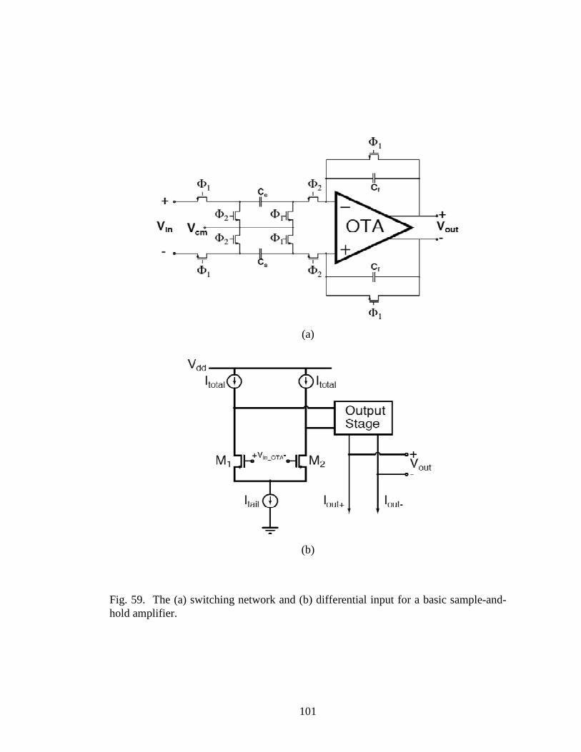
101
Fig. 59. The (a) switching network and (b) differential input for a basic sample-and-hold amplifier.
(a)
(b)
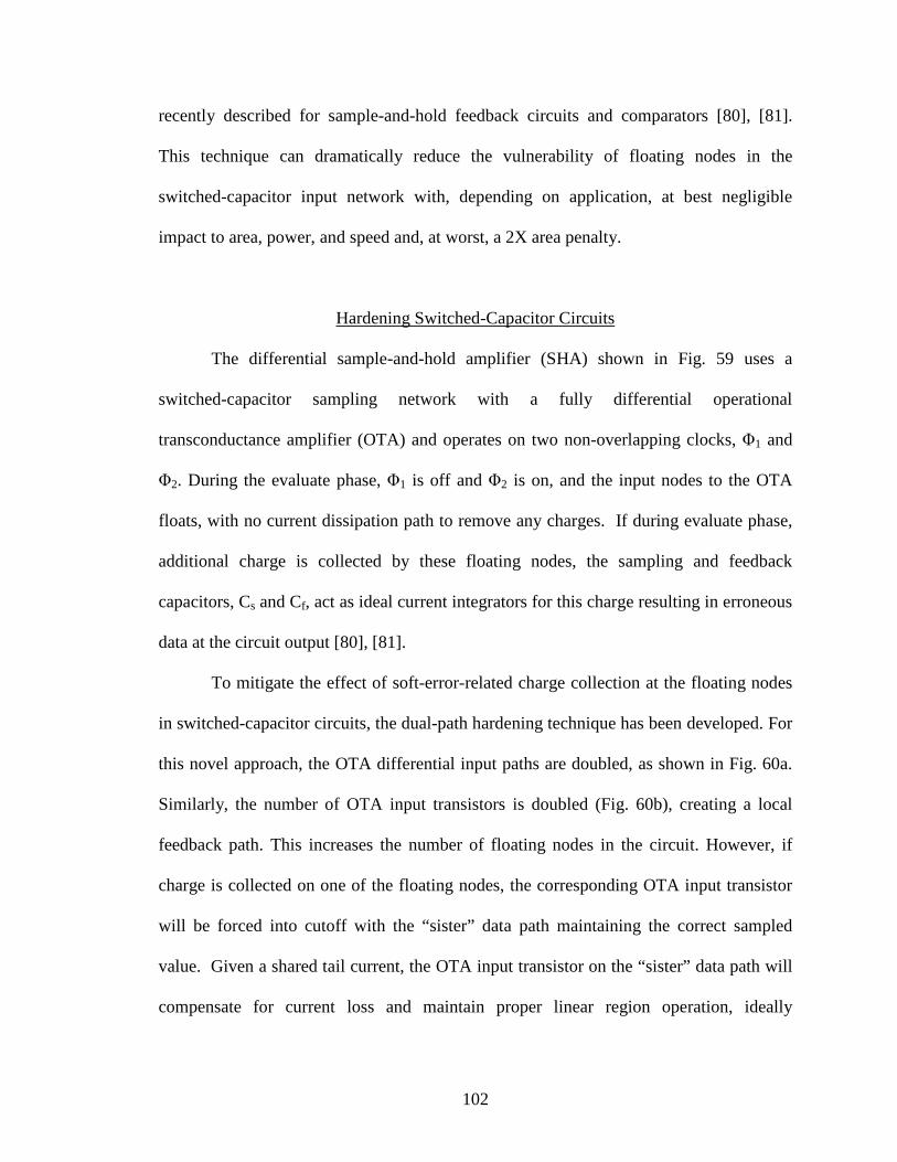
102
recently described for sample-and-hold feedback circuits and comparators [80], [81].
This technique can dramatically reduce the vulnerability of floating nodes in the
switched-capacitor input network with, depending on application, at best negligible
impact to area, power, and speed and, at worst, a 2X area penalty.
Hardening Switched-Capacitor Circuits
The differential sample-and-hold amplifier (SHA) shown in Fig. 59 uses a
switched-capacitor sampling network with a fully differential operational
transconductance amplifier (OTA) and operates on two non-overlapping clocks, Φ1 and
Φ2. During the evaluate phase, Φ1 is off and Φ2 is on, and the input nodes to the OTA
floats, with no current dissipation path to remove any charges. If during evaluate phase,
additional charge is collected by these floating nodes, the sampling and feedback
capacitors, Cs and Cf, act as ideal current integrators for this charge resulting in erroneous
data at the circuit output [80], [81].
To mitigate the effect of soft-error-related charge collection at the floating nodes
in switched-capacitor circuits, the dual-path hardening technique has been developed. For
this novel approach, the OTA differential input paths are doubled, as shown in Fig. 60a.
Similarly, the number of OTA input transistors is doubled (Fig. 60b), creating a local
feedback path. This increases the number of floating nodes in the circuit. However, if
charge is collected on one of the floating nodes, the corresponding OTA input transistor
will be forced into cutoff with the “sister” data path maintaining the correct sampled
value. Given a shared tail current, the OTA input transistor on the “sister” data path will
compensate for current loss and maintain proper linear region operation, ideally
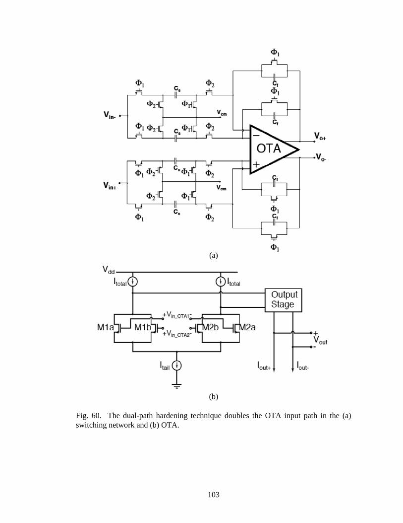
103
Fig. 60. The dual-path hardening technique doubles the OTA input path in the (a) switching network and (b) OTA.
(a)
(b)
104
correcting any error. This technique works best when the amplifier input transistor is
forced into cutoff. To ensure this, the switches must be of same type (NFET or PFET) as
the OTA input transistors. This design constraint can lead to some difficulty in designing
a circuit with strict noise margins, but can be overcome if bootstrapped switches are used.
Area, power, and speed design penalties associated with the dual-path hardening
technique are minimal. If capacitor values are set by gain-bandwidth and thermal noise
requirements, then the sizes of capacitors, switches, and amplifier input transistors can be
divided between the branches, with negligible impact on final area, power and speed [81],
as is the case in the present SHA example. In the worst-case scenario, if the capacitor
values are small enough to be dominated by parasitic effects, and cannot be halved [80],
the circuit area doubles, assuming the design is dominated by capacitor area. In this case,
the switching-network power requirements will also be doubled, but is negligible
compared to the amplifier power requirements. Speed penalties will depend on the
driving circuit; if the driver is slew-rate limited then speed may also be halved.
Test Chip
Multiplying Digital-to-Analog Converter
The dual path technique was implemented on a multiplying digital-to-analog
converter circuit (MDAC) and a comparator circuit. Baseline (conventional design
without the dual paths mentioned above) and hardened (with dual paths) versions were
fabricated in AMI 0.5 µm bulk CMOS process. Even though results presented in this
paper are for 0.5 µm process, this technique is equally effective for any advanced
technology node.

105
The baseline, 2X gain, MDAC switched-capacitor network, shown in Fig. 61, is
similar to the SHA. During sample phase, Φ1 is off and Φ2 is on, the input signal is
sampled across both equal-sized sampling and feedback capacitors, Cs and Cf:
( )( ) CVVQ
CVVQ
cmSINsamp
cmSINsamp
2
2
∗−=
∗−=
−−
++
(23).
During evaluate phase, Φ1 is on and Φ2 is off, the sampling capacitors’ bottom plate is
connected to VREF and the feedback capacitors are connected into negative feedback.
Fig. 61. Schematic of the baseline, 2X gain, multiplying digital-to-analog converter switched-capacitor network.
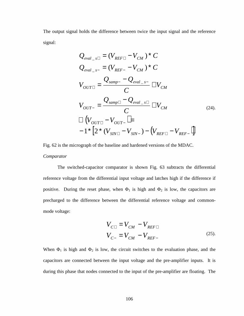
106
The output signal holds the difference between twice the input signal and the reference
signal:
( )( )[ ]−+−+
−+
++−
−−+
−−
++
−−−∗∗−=−∴
+−
=
+−
=
∗−=
∗−=
REFREFSINSIN
OUTOUT
CMsevalsamp
OUT
CMsevalsamp
OUT
CMREFseval
CMREFseval
VVVV
VV
VC
QQV
VC
QQV
CVVQ
CVVQ
)(21
)(
)(
_
_
_
_
(24).
Fig. 62 is the micrograph of the baseline and hardened versions of the MDAC.
Comparator
The switched-capacitor comparator is shown Fig. 63 subtracts the differential
reference voltage from the differential input voltage and latches high if the difference if
positive. During the reset phase, when Φ1 is high and Φ2 is low, the capacitors are
precharged to the difference between the differential reference voltage and common-
mode voltage:
−−
++
−=−=
REFCMC
REFCMC
VVV
VVV (25).
When Φ1 is high and Φ2 is low, the circuit switches to the evaluation phase, and the
capacitors are connected between the input voltage and the pre-amplifier inputs. It is
during this phase that nodes connected to the input of the pre-amplifier are floating. The
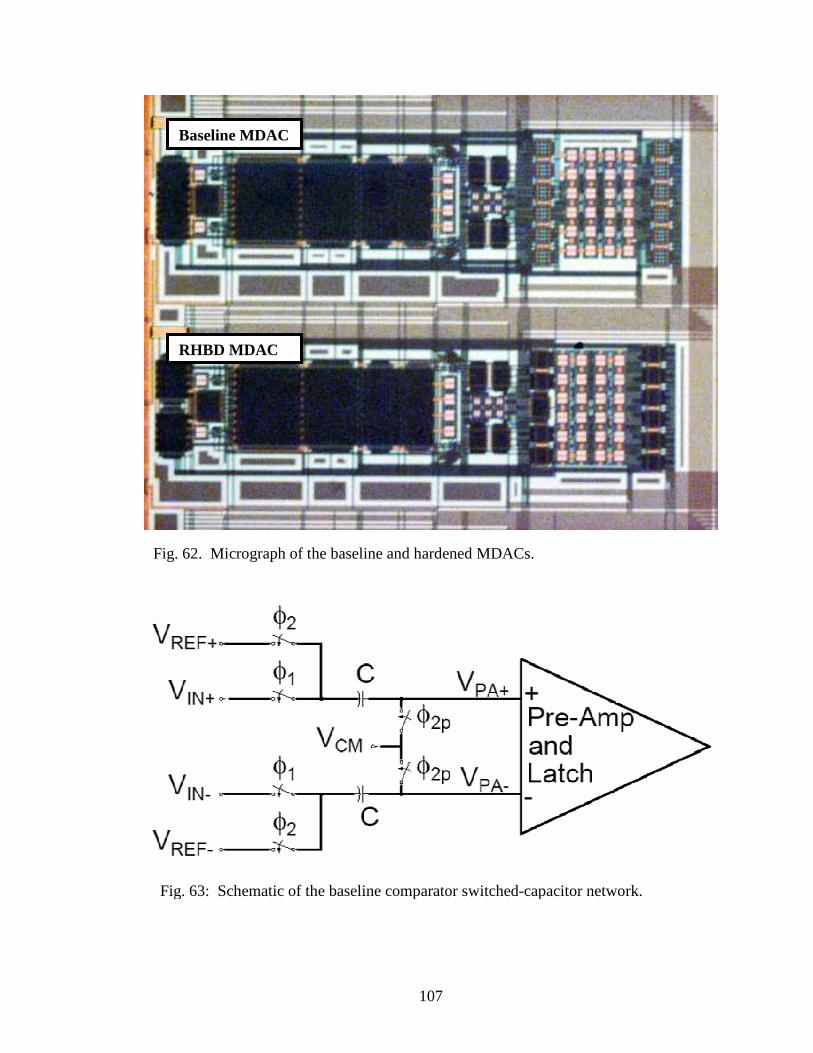
107
Fig. 63: Schematic of the baseline comparator switched-capacitor network.
Fig. 62. Micrograph of the baseline and hardened MDACs.
Baseline MDAC
RHBD MDAC
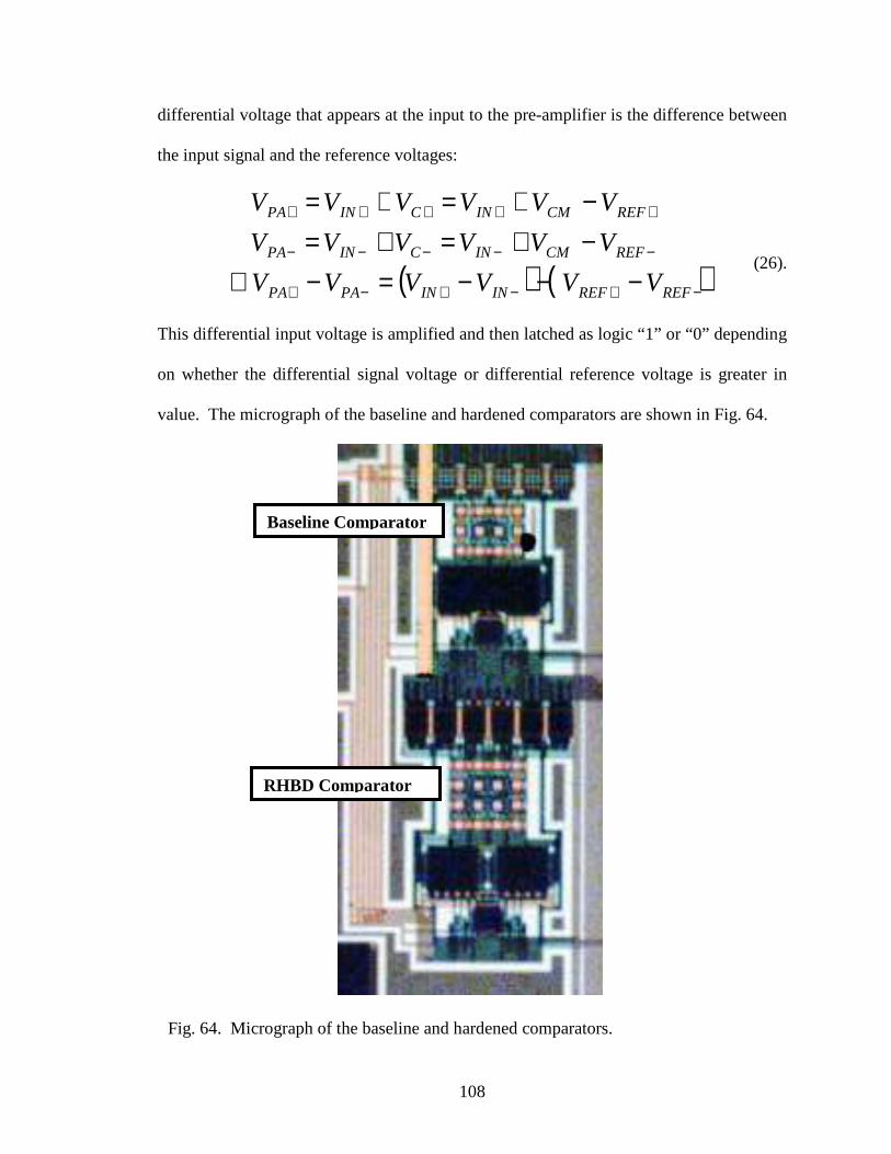
108
differential voltage that appears at the input to the pre-amplifier is the difference between
the input signal and the reference voltages:
( ) ( )−+−+−+
−−−−−
+++++
−−−=−∴−+=+=−+=+=
REFREFININPAPA
REFCMINCINPA
REFCMINCINPA
VVVVVV
VVVVVV
VVVVVV
(26).
This differential input voltage is amplified and then latched as logic “1” or “0” depending
on whether the differential signal voltage or differential reference voltage is greater in
value. The micrograph of the baseline and hardened comparators are shown in Fig. 64.
Fig. 64. Micrograph of the baseline and hardened comparators.
Baseline Comparator
RHBD Comparator
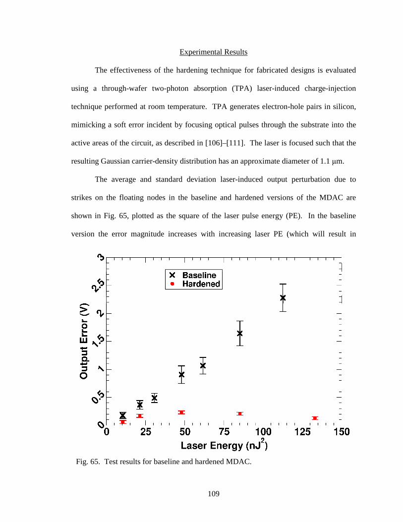
109
Experimental Results
The effectiveness of the hardening technique for fabricated designs is evaluated
using a through-wafer two-photon absorption (TPA) laser-induced charge-injection
technique performed at room temperature. TPA generates electron-hole pairs in silicon,
mimicking a soft error incident by focusing optical pulses through the substrate into the
active areas of the circuit, as described in [106]–[111]. The laser is focused such that the
resulting Gaussian carrier-density distribution has an approximate diameter of 1.1 µm.
The average and standard deviation laser-induced output perturbation due to
strikes on the floating nodes in the baseline and hardened versions of the MDAC are
shown in Fig. 65, plotted as the square of the laser pulse energy (PE). In the baseline
version the error magnitude increases with increasing laser PE (which will result in
Fig. 65. Test results for baseline and hardened MDAC.
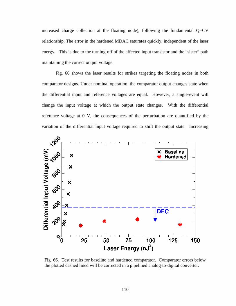
110
increased charge collection at the floating node), following the fundamental Q=CV
relationship. The error in the hardened MDAC saturates quickly, independent of the laser
energy. This is due to the turning-off of the affected input transistor and the “sister” path
maintaining the correct output voltage.
Fig. 66 shows the laser results for strikes targeting the floating nodes in both
comparator designs. Under nominal operation, the comparator output changes state when
the differential input and reference voltages are equal. However, a single-event will
change the input voltage at which the output state changes. With the differential
reference voltage at 0 V, the consequences of the perturbation are quantified by the
variation of the differential input voltage required to shift the output state. Increasing
Fig. 66. Test results for baseline and hardened comparator. Comparator errors below the plotted dashed lined will be corrected in a pipelined analog-to-digital converter.
111
deposited charge forces the baseline comparator to change state at a larger-than-normal
differential input voltage. This is analogous to the baseline MDAC response of Fig. 65:
the hardened comparator error response quickly saturates with increasing charge
injection.
There are comparator applications that can correct the remaining error in the data
seen in Fig. 66 for the hardened design. To further clarify the effectiveness of the dual-
path hardening technique, consider a pipelined A-to-D converter. Typically each pipeline
stage will overlap with the next stage, providing some digital error correction (DEC) for
voltage errors less than ½ LSB resulting in the comparators. Assuming a 1.5-bit stage
and VREF of 3 V, the DEC will correct all errors less than 375 mV for these designs.
Thus, proposed single-event mitigation technique will correct all single-events on the
hardened floating nodes.
Conclusions to Dual-Path Hardening Experimental Validation
The dual-path RHBD technique provides a simple but effective means of
hardening the floating input nodes for switched-capacitor circuits. By splitting the input
nodes into separate parallel signal paths, a dramatic improvement in single-event
hardness is observed. In non-hardened switched-capacitor designs a single-event on the
floating nodes will cause an error at the output directly proportional to the amount of
charge collected. The dual-path RHBD technique limits the size of any remaining error
and decouples the error response from the amount of charge collected. In some switched-
capacitor circuit applications the hardening technique will make the floating nodes
immune to single-events. For example in a pipelined ADC, the input voltage region over
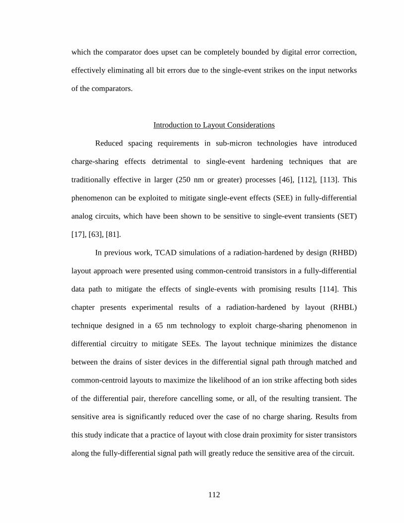
112
which the comparator does upset can be completely bounded by digital error correction,
effectively eliminating all bit errors due to the single-event strikes on the input networks
of the comparators.
Introduction to Layout Considerations
Reduced spacing requirements in sub-micron technologies have introduced
charge-sharing effects detrimental to single-event hardening techniques that are
traditionally effective in larger (250 nm or greater) processes [46], [112], [113]. This
phenomenon can be exploited to mitigate single-event effects (SEE) in fully-differential
analog circuits, which have been shown to be sensitive to single-event transients (SET)
[17], [63], [81].
In previous work, TCAD simulations of a radiation-hardened by design (RHBD)
layout approach were presented using common-centroid transistors in a fully-differential
data path to mitigate the effects of single-events with promising results [114]. This
chapter presents experimental results of a radiation-hardened by layout (RHBL)
technique designed in a 65 nm technology to exploit charge-sharing phenomenon in
differential circuitry to mitigate SEEs. The layout technique minimizes the distance
between the drains of sister devices in the differential signal path through matched and
common-centroid layouts to maximize the likelihood of an ion strike affecting both sides
of the differential pair, therefore cancelling some, or all, of the resulting transient. The
sensitive area is significantly reduced over the case of no charge sharing. Results from
this study indicate that a practice of layout with close drain proximity for sister transistors
along the fully-differential signal path will greatly reduce the sensitive area of the circuit.
113
Background
The advantages in dynamic output range and noise rejection over single-ended
circuits make differential topologies the accepted standard for high-performance analog
design [113]. The sample and hold amplifier (SHA), shown in Fig. 59, has several
examples of “sister” differential devices in the data path. These device pairs feature two
transistors connected such that any differential voltage applied to the inputs is amplified,
making single events (SE) particularly detrimental. However, assuming a large common
mode rejection ratio (CMRR), any common voltage applied to both the inputs is rejected,
as illustrated in Fig. 67.
When device matching is a priority in analog layout, a common-centroid approach
is used in which devices are arranged around a center location so that the effects of
process variation, gradient effects, and random noise are cancelled [115]. This is typical
Fig. 67. Illustration of single-ended and fully differential operation. An injected transient on a single-ended amplifier will be propagated with the signal while a transient shared by the inputs of a fully-differential amplifier will be cancelled.

114
in differential pair inputs, but not necessarily used for other sister devices along a
differential signal path such as switching transistors.
For advanced technologies, the density of transistors is sufficiently high that
charge generated by a single-event will be collected by the struck transistor and adjacent
components. If a common-centroid layout is used to promote charge sharing in a fully
differential circuit, the effects of a single-event transient on the circuit can be minimized.
Test Design and Circuit Operation
Proposed RHBL examples for single-multiplicity (M1) and unit-cell double-
multiplicity (M2) transistor differential pairs are shown in Fig. 68. These pairs are
arranged with drains located as close as design rules allow or, when applicable, in a
common-centroid configuration.
The circuit used in this study to test the effectiveness of the layout technique for
mitigating SEEs is shown in Fig. 69. The circuit is designed in a 65 nm process and is
based on a charge-sharing measurement circuit described previously [116]. Separate test
circuits are available for M1 and M2 configured as in Fig. 68. The bottom panel of
Fig. 69 shows the layout for M2.
During an SEE test of this circuit, there are three phases of operation: pre-charge,
hit, and evaluate. During pre-charge, the 516 fF target capacitors are charged to a test-
controlled voltage and the reference voltage is set. During the laser strike, all of the
switches are open and the target nodes are floating. As a result of the hit, some charge
stored on the target capacitors is removed. Finally, during the evaluate phase, the sense
amps are enabled to compare each transistor to the reference voltage.

115
The efficacy of this approach is evaluated using a through-wafer two-photon
absorption (TPA) single event upset mapping technique [106]-[111], as previously
described in Chapter VII. The pre-charge and evaluate clock cycles for the circuit are
synchronized with the laser pulse. The timing of the clocks with the laser ensures each
laser pulse hits the target shortly after pre-charging and just before evaluation, ensuring
an event occurs at each evaluate phase and that there are no strikes during the pre-charge
phase, which would potentially distort the results.
The M1 and M2 target devices were scanned by the laser with a step size of
0.3 µm. Data were taken at a low enough laser pulse energy (2.86 nJ) so no upsets are
observed above a 950 mV target voltage in the most sensitive region of the circuit,
ensuring that the upset voltage could be observed throughout the circuit. For each
location in a scan, pre-charge voltage at the hit nodes is swept in 25 mV steps with
respect to the reference voltage. The voltage at which the sense amp switches states is
Fig. 68. Proposed charge-sharing layout designs RHBL M1 (top) and RHBL M2 (bottom).
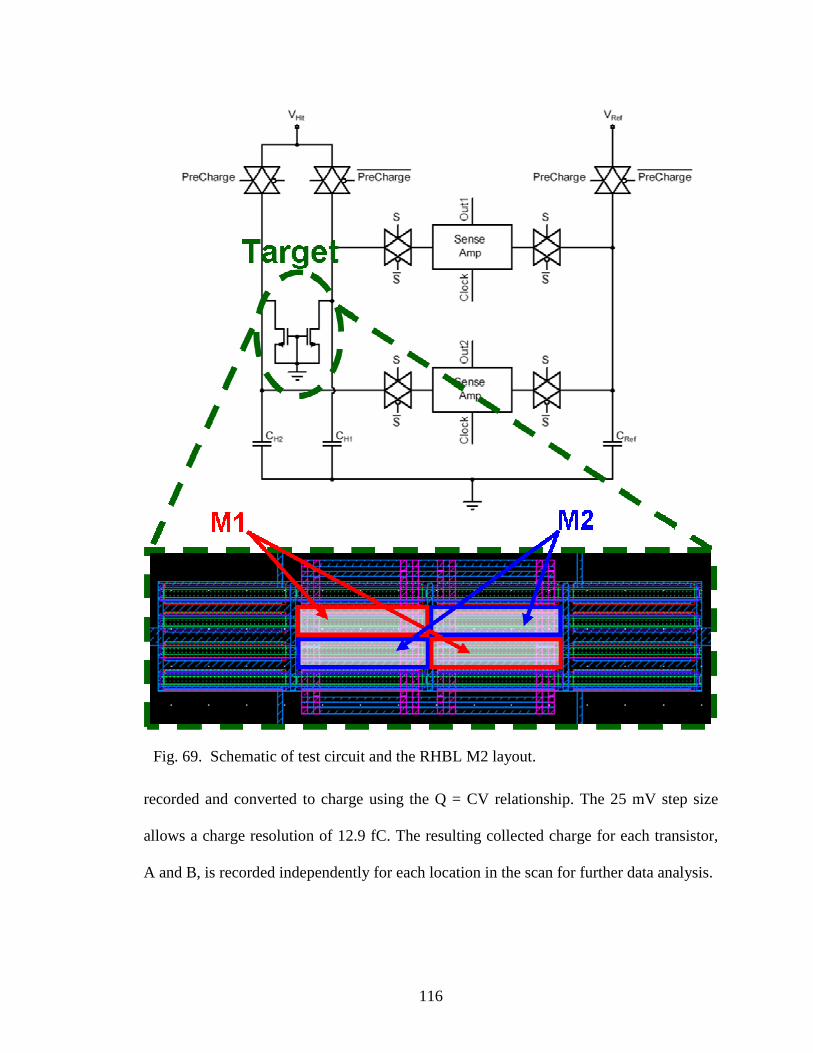
116
recorded and converted to charge using the Q = CV relationship. The 25 mV step size
allows a charge resolution of 12.9 fC. The resulting collected charge for each transistor,
A and B, is recorded independently for each location in the scan for further data analysis.
Fig. 69. Schematic of test circuit and the RHBL M2 layout.
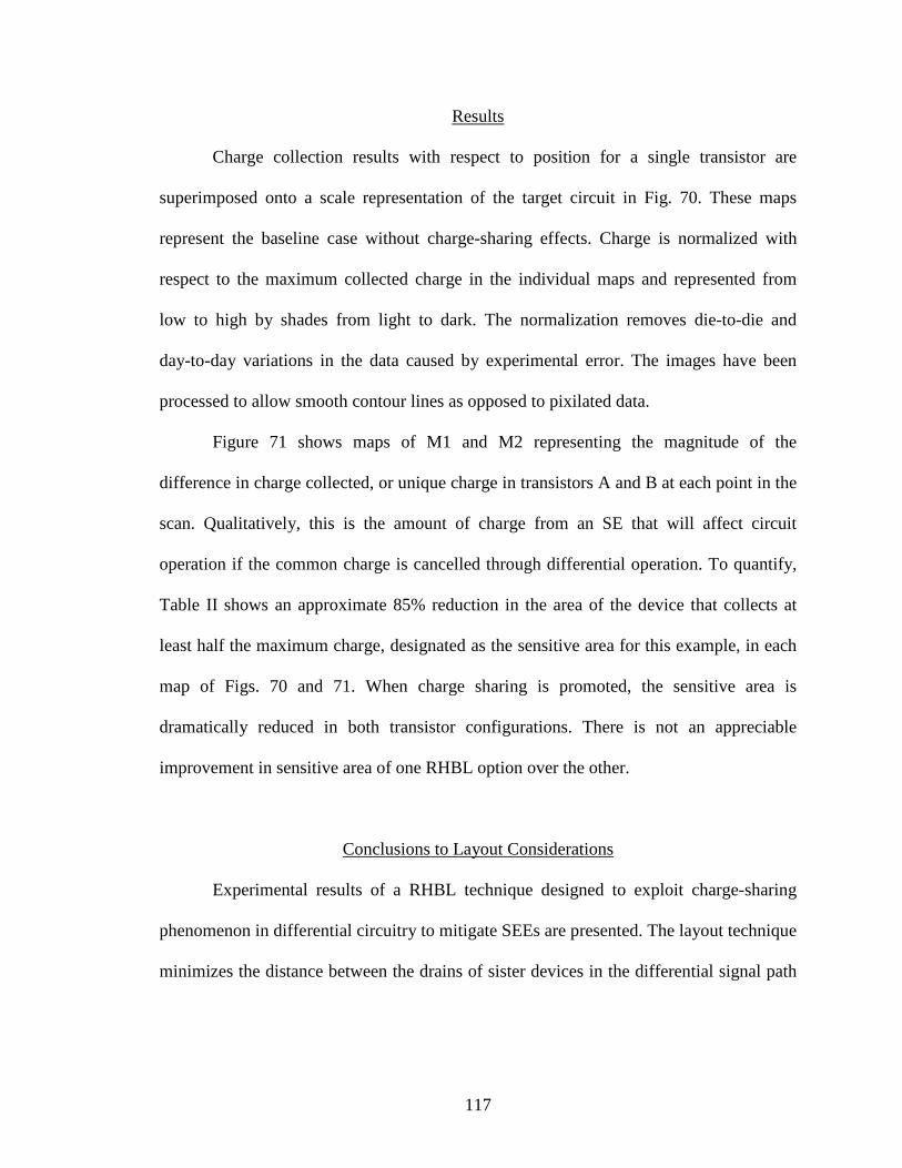
117
Results
Charge collection results with respect to position for a single transistor are
superimposed onto a scale representation of the target circuit in Fig. 70. These maps
represent the baseline case without charge-sharing effects. Charge is normalized with
respect to the maximum collected charge in the individual maps and represented from
low to high by shades from light to dark. The normalization removes die-to-die and
day-to-day variations in the data caused by experimental error. The images have been
processed to allow smooth contour lines as opposed to pixilated data.
Figure 71 shows maps of M1 and M2 representing the magnitude of the
difference in charge collected, or unique charge in transistors A and B at each point in the
scan. Qualitatively, this is the amount of charge from an SE that will affect circuit
operation if the common charge is cancelled through differential operation. To quantify,
Table II shows an approximate 85% reduction in the area of the device that collects at
least half the maximum charge, designated as the sensitive area for this example, in each
map of Figs. 70 and 71. When charge sharing is promoted, the sensitive area is
dramatically reduced in both transistor configurations. There is not an appreciable
improvement in sensitive area of one RHBL option over the other.
Conclusions to Layout Considerations
Experimental results of a RHBL technique designed to exploit charge-sharing
phenomenon in differential circuitry to mitigate SEEs are presented. The layout technique
minimizes the distance between the drains of sister devices in the differential signal path

118
Fig. 70. Baseline case of charge collection on a single transistor without the effects of charge sharing for M1 and M2.
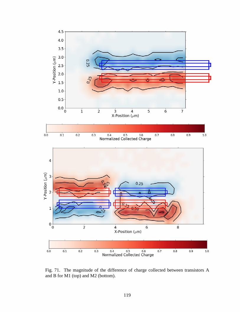
119
Fig. 71. The magnitude of the difference of charge collected between transistors A and B for M1 (top) and M2 (bottom).
120
through matched and common-centroid techniques to maximize the likelihood of an ion
strike affecting both sides of the differential pair, therefore cancelling some, or all, of the
resulting transient. The sensitive area for both layout techniques is reduced by a factor of
at least 6.5 over the baseline case of no charge sharing. There is neither penalty nor
benefit for using a common-centroid layout in the case where the transistors need to be
separated into unit cells as long as the drains of the devices are placed as close together as
design rules allow. These tests were conducted with only n-channel devices. It is
expected that p-channel devices will only enhance the charge sharing phenomena [116].
Analysis of the symmetry of the devices using a quadrant of the experimental data
mirrored upon itself to reduce experimental variation will be fully described in the final
paper. The results from this study indicate that a practice of layout with close drain
proximity for sister transistors along the fully-differential signal path will greatly reduce
the sensitive area of the circuit. The penalty is additional wiring overhead and additional
capacitance in the cases where common-centroid layout would not normally be
employed, but the overall charge sharing, and therefore single-event mitigation, is
dramatically enhanced.
TABLE II SENSITIVE AREAS COLLECTING UNIQUE CHARGE GREATER THAN HALF OF THE MAXIMUM
DEPOSITED CHARGE FOR BASELINE AND RHBL M1 AND M2. M1 (µm2) M2 (µm2)
Baseline 6.39 12.24
RHBL 0.94 1.85
121
CHAPTER VIII
CONCLUSIONS
Conclusion
This research uses circuit simulations, behavioral modeling, and experimental
testing to characterize the effects of SEEs and provide novel RHBD techniques for
generalized pipelined ADC circuits. First, a metric for comparing SE-vulnerability
between multiple designs was developed. Signal-to-noise ratio provides an excellent
metric when comparing different single-event mitigation design choices in an ADC. The
most significant advantage of using SNR is not to evaluate the performance of one
particular circuit, but to compare the performance of two or more different RHBD
techniques on the same circuit or system, or to compare the relative hardn.ess of two or
more different circuit topologies. In such situations, the simulated error rate can be set
sufficiently high enough to allow the designer to make a valid comparison between
designs. Because signal-to-noise ratio is so commonly used to characterize analog and
mixed-signal systems, the SNR metric should prove equally useful in quantifying the
benefit of future RHBD techniques applied to a very broad range of designs such as
analog-to-digital converters, digital-to-analog converters, RF circuits, and analog signal
processing circuits.
The single-event sensitivity of pipelined ADCs with multi-bit stages has been
analyzed and compared to 1.5-bit stage alternatives. Multi-bit stages are commonly used
in high-resolution pipelined ADC designs to provide reduced thermal noise, area, and
122
power. Multi-bit stages can also provide advantages with respect to single-event
vulnerability when compared to 1.5-bit stages. By utilizing a more robust encoding
scheme with little area penalty, errors resulting from comparator upsets in a multi-bit
stage can be limited to one LSB with a topology nearly as effective as 1.5-bit stages using
comparator TMR in the first pipeline stage. Pipelined ADCs with multi-bit stages will
also have fewer MDACs, leading to less sensitive area, although it may be necessary to
increase capacitor values in order to decrease SE errors resulting from strikes in the
MDACs. These results indicate that with proper design, pipelined ADCs using multi-bit
stages can be as effective as, and much more robust than, their 1.5-bit stage counterparts
when mitigating single-event errors in radiation environments.
Previous SE-hardening recommendations have been limited to hardening the
digital circuits or increasing the sizes of sampling capacitors in the analog circuits. This
work has expanded and provides much more thorough designs for hardening pipelined
ADCs. 1.5-bit stages can benefit by applying TMR to the comparators. SE-sensitivity to
comparator upset in multi-bit stages can been masked and/or corrected by using better
robust encoding logic schemes. Also, the analog circuitry has less sensitive area in
pipelined ADC designs using multi-bit stages than 1.5-bit stages.
The comparators, sample-and-hold amplifier, and multiplying digital-to-analog
converter sub-circuits are likely to be fully-differential and use switched-capacitor
circuits in advanced high-performance designs. Until recently switched-capacitor
circuits were highly vulnerable to SE because of floating nodes. Hardening options were
limited to resizing the sampling capacitors. A novel RHBD technique, dual path
hardening, has been developed that significantly decreases the SE-vulnerability of
123
switched-capacitor circuits and is applicable in both closed-loop and open-loop designs.
Results from simulations and laser testing have validated dual-path hardening.
Signal information in fully-differential analog circuits is stored as the difference
of two data paths. This significantly improves the noise margins since noise shared
across both data paths does not affect the signal information. While charge sharing is a
major issue in highly-scaled digital circuits, it can be advantageous in analog circuits.
Results from recent laser testing have validated layout techniques that share charge more
efficiently thus providing improved SE-hardening in fully-differential analog circuits.
Design Techniques for SE-Hardened Pipelined ADCs
Unless SE radiation-hardened-by-design (RHBD) techniques are used, pipelined
ADCs will be sensitive to single-events. The majority of previous work has focused on
hardening the digital circuitry through various techniques: temporal-hardening, resistive
feedback, and TMR [61]-[66], [69]. However, the analog sub-circuits are vulnerable to
single-events as well and prior to this work hardening options were limited to increasing
the size of the sampling capacitors, increasing nodal capacitance, and using auto-zeroing
switched-capacitor architectures to restrain the duration or error [63], [64], [68].
This work has led to many additional recommendations for hardening pipelined
ADCs. Since each pipeline stage quantizes the signal with decreasing significance; the
effort of SE hardening should focus with the beginning stages. Simple architecture
changes can limit output errors produced by comparator upsets. Comparator TMR is
very effective in 1.5-bit stages, but, in multi-bit stages can have a high cost in terms of
area and power. While traditional encoder logic schemes in multi-bit stages are effective
124
for protecting against metastability issues, they are still vulnerable to SEs. Instead, robust
logic schemes can be implemented, such as equation (19), that will either correct or mask
many errors. In advanced designs the analog/mixed-signal sub-circuits (comparator,
sample-and-hold amplifier, and multiplying digital-to-analog converter) are likely to use
switched-capacitor topologies. Unfortunately switched-capacitor circuits contain floating
nodes which produce larger errors from charge collection. Dual-path hardening has been
developed and experimentally verified for hardening the vulnerable floating nodes in
switched-capacitor designs with minimal tradeoffs. Advanced analog/mixed-signal
designs are also fully-differential, therefore sensitive area can be significantly decreased
through layout considerations. “Sister” devices across the differential data paths should
be placed as close as possible in layout and even use common-centroid or interleaved
geometries. This will promote common-mode charge, which is easily distinguishable
from the data signal and is rejected by amplifiers.
The pipelined ADC signal path can be hardened by combining the analog/mixed-
signal RHBD techniques developed in this work with the previous recommendations for
digital logic and latches. The reference voltage and clock circuits are also vulnerable to
single-events, but were not covered in this work. Steps must be taken to harden these
control circuits as well.
125
REFERENCES
[1] T. C. May and M. H. Woods, “Alpha Particle-Induced Soft Errors in Dynamic Memories,” IEEE Trans. Elec. Dev., vol. 26, no. 1, pp. 2-9, Jan. 1979.
[2] E. Normand, “Single Event Effects in Avionics,” IEEE Trans. Nucl. Sci., vol.
43, no. 2, pp. 461-474, April 1996. [3] H. C. Koons, J. E. Mazur, R. S. Selesnick, J. B. Blake, J. F. Fennell, J. L.
Roeder, and P. C. Anderson, “The impact of the space environment on space systems,” Aerospace Technical Report, no. TR-99(1670)-1, July, 1999.
[4] P. D. Bradley and E. Normand, “Single Event Upsets in Implantable
Cardioverter Defibrillators,” IEEE Trans. Nucl. Sci., vol. 45, no. 6, pp. 2929-2939, Dec. 1998.
[5] J. Wilkinson and S. Hareland, “A Cautionary Tale of Soft Errors Induced by
SRAM Packaging Materials,” IEEE Trans. Dev. And Mat. Reliab., vol. 5, no. 3, pp. 428-433, Sept. 2005.
[6] T. L. Turflinger, M. V. Davey, “Transient radiation test techniques for high-
speed analog-to-digital converters,” IEEE Trans. Nuc. Sci., vol. 36, no. 6, pp. 2356-2361, Dec. 1989.
[7] T. L. Turflinger and M. V. Davey, “Understanding Single Event Phenomena
in Complex Analog and Digital Integrated Circuits,” IEEE Trans. Nucl. Sci., vol. 37, no. 6, pp. 1832-1838, Dec. 1990.
[8] D. J. Wilson and D. A. Dorn, “Characterization of single event effects for the
AD677, 16 bit A/D converter,” Proc. IEEE Radiation Effects Data Workshop, pp. 113-117, 2007.
[9] R. A. Reed, P. W. Marshall, M. A. Carts, G. L. Henegar, and R. B. Katz,
“Proton-induced single event upset characterization of a 1 giga-sample per second analog-to-digital convert,” Radiation and Its Effects on Components and Systems, 1999 Fifth European Conference on, pp. 188-192, 1999.
[10] S. P. Buchner, T. J. Meehan, A. B. Campbell, K. A. Clark, D. McMorrow,
“Characterization of single-event upsets in a flash analog-to-digital converter (AD9058),” IEEE Trans. Nucl. Sci., vol. 47, no. 6, pp. 2358-2364, 2000.
[11] S. Buchner, A. B. Campbell, A. Sternberg, L. W. Massengill, D. McMorrow,
C. Dyer, “Validity of using a fixed analog input for evaluating the SEU sensitivity of a flash analog-to-digital converter,” IEEE Trans. Nucl. Sci., vol. 52, no. 1, pp. 462-467, Feb. 2005.

126
[12] W. F. Heidergott, R. Ladbury, P. W. Marshall, S. Buchner, A. B. Campbell,
R. A. Reed, J. Hockmuth, N. Kha, C. Sieleck, A. Assad, “Complex SEU signatures in high-speed analog-to-digital conversion,” IEEE Trans. Nucl. Sci., vol. 48, no. 6, pp. 1828-1832, Dec. 2001.
[13] K. Kruckmeyer, R. L. Rennie, and V. Ramachandran, “Use of Code Error and
Beat Frequency Test Method to Identify Single Event Upset Sensitive Circuits in a 1 GHz Analog to Digital Converter,” IEEE Trans. Nucl. Sci., vol. 55, no. 4, pp. 2013-2018, Aug. 2008.
[14] K. G. Merkel and A. L. Wilson, “A survey of high performance analog-to-
digital converters for defense space applications,” Aerospace Conference, Proceedings, 2003 IEEE, vol. 5, pp. 2415-2427, Mar. 2003.
[15] Y. Boulghassoul, S. Buchner, D. Morrow, V. Pouget, L. W. Massengill, P.
Fouillat, W. T. Holman, C. Poivey, J. W. Howard, M. Savage, M. C. Maher, “Investigation of millisecond-long analog single-event transisents in the LM6144 op amp,” IEEE Trans. Nucl. Sci., vol. 51, no. 6, pp. 3529, 3536, Dec. 2004.
[16] Y. Boulghassoul, L. W. Massengill, A. L. Sternberg, B. L. Bhuva, “Effects of
technology scaling on the SET sensitivity of RF CMOS Voltage-controlled oscillators,” IEEE Trans. Nucl. Sci., vol. 52, no. 6, pp. 2426-2432, Dec. 2005.
[17] T. D. Loveless, L. W. Massengill, B. L. Bhuva, W. T. Holman, A. F. Witulski,
and Y. Boulghassoul, “A hardened-by-design technique for RF digital phase-locked-loops,” IEEE Trans. Nucl. Sci., vol. 53, no. 6, pp. 3432–3438, Dec. 2006.
[18] J. T. Wallmark and S. M. Marcus, “Minimum size and maximum packing
density of nonredundant semiconductor devices,” Proc. IRE, vol. 50, pp. 286–298, 1962.
[19] C. W. Gwyn, D. L. Scharfetter, J. L. Wirth, “The Analysis of Radiation
Effects in Semiconductor Devices,” IEEE Trans. Nucl. Sci., vol. 14, no. 6, pp. 153-169, Dec. 1967.
[20] V. A. J. van Lint, J. H. Alexander, D. K. Nichols, P. R. Ward, “Computerized
Model for Response of Transistors to a Pulse of Ionizing Radiation,” IEEE Trans. Nucl. Sci., vol. 14, no. 6, pp. 170-178, Dec. 1967.
[21] D. Binder, E. C. Smith, A. B. Holman, “Satellite Anomalies from Galactic
Cosmic Rays,” IEEE Trans. Nucl. Sci., vol. 22, no. 6, pp. 2675-2680, Dec. 1975.

127
[22] G. E. Moore, “Progress in Digital Integrated Electronics,” IEDM Tech. Dig., vol. 21, pp. 11-13, 1975.
[23] T. R. Oldham, “How Device Scaling Affects Single Event Sensitivity,” in
IEEE NSREC Short Course, 2003, pp. IV-1–IV-66. [24] J. Mazur, “The Radiation Environment Outside and Inside a Spacecraft,” in
IEEE NSREC Short Course, 2002, pp. II-1–II-69. [25] Nikkei Science, Inc. of Japan, image by K. Endo. [26] J. A. Van Allen, C. E. McIlwain, and G. H. Ludwig, “Radiation observations
with satellite 1958 EX,” J. Geophys. Res., vol. 64, no. 3, pp. 271–286, 1959. [27] W. J. Stapor, P. T. McDonald, A. R, Knudson, A. B. Campbell, and B. G.
Glagola, “Charge Collection in Silicon for Ions of Different Energy but Same Linear Energy Transfer (LET),” IEEE Trans. on Nucl. Sci., vol. 35, no. 6, pp. 1585–1590, Dec. 1988.
[28] M. Xapsos, “Modeling the Space Radiation Environment,” in IEEE NSREC
Short Course, 2006, pp. II-1–II-62. [29] E. G. Stassinopoulos, J. P. Raymond, “The Space Radiation Environment for
Electronics,” IEEE Proceedings, vol. 76, no. 11, pp. 1423-1442, Nov. 1988. [30] J. Barth, “Modeling Space Radiation Environments,” in IEEE NSREC Short
Course, 1997, pp. I-1-I-83. [31] National Aeronautics and Space Administration's Goddard Space Flight
Center, Solar & Heliospheric Observatory (SOHO) Project. [Online]. Available: http://sohowww.nascom.nasa.gov/gallery/images/cycle001.html
[32] R. A. Mewaldt, M. D. Looper, C. M. S. Cohen, G. M. Mason, D. K. Haggerty,
M. I. Desai, A. W. Labrador, R. A. Leske, J. E. Mazur, “Solar-Particle Energy Spectra during the Large Events of October-November 2003 and January 2005,” 29th International Cosmic Ray Conference, June 2005.
[33] R. A. Medwadlt, “Elemental Composition and Energy Spectra of Galactic
Cosmic Rays,” Proc. from Conference on Interplanetary Particle Environment, JPL Publication 88-28, pp. 121-132, JPL, Pasadena, CA, April 1988.
[34] T. C. May and M. H. Woods, “A New Physical Mechanism for Soft Error in
Dynamic Memories,” Proc. 16th Int’l Reliability Physics Symp. (IRPS), IEEE EDS, pp. 33-40, 1978.
128
[35] A. Maheshwari and A. Lesea, “Flip-Chip Package Substrate Solder Issue,” Xilinx White Paper: Virtex-II and Virtex-II Pro Families, WP208(v1.1), pp. 1-4, Jan. 2004.
[36] R. L. Fleischer, “Cosmic Ray Interaction with Boron: A Possible Source of
Soft Errors,” IEEE Trans. Nucl. Sci., vol. 30, no. 5, pp. 4013-4015, Oct. 1983. [37] T. R. Oldham, S. Murril, and C. T. Self, “Single Event Upset of VLSI
Memory Circuits Induced by Thermal Neutrons,” Hardened Electronics and Radiation Technology Conference, 1986.
[38] S. M. Sze, Physics of Semiconductor Devices, Wiley, New York, 1981. [39] L. W. Massengill, “SEU modeling and prediction techniques,” in IEEE
NSREC Short Course, 1993, pp. III-1–III-93. [40] S. Buchner, “Single-Event Transients in Linear Integrated Circuits,” in IEEE
NSREC Short Course, 2005, pp. IV-1-IV-77. [41] R. D. Evans, The Atomic Nucleus, McGraw-Hill Book Company, Inc, New
York, 1955. [42] C. M. Hsieh, P. C. Murley, and R. R. O’Brien, “A field-funneling effect on
the collection of alpha-particle-generated carriers in silicon devices,” IEEE Electron Device Lett., vol. 2, pp. 103-105, Dec. 1981.
[43] R. Baumann, “Single-event effects in advanced CMOS,” in IEEE NSREC
Short Course, 2005, pp. II-1–II-59. [44] A. K. Sutton, J. D. Cressler, M. A. Carts, P. W. Marshall, J. A. Pellish, R. A.
Reed, M. L. Alles, N. Guogu, “Proton-induced SEU in SiGe digital logic at cryogenic temperatures,” Int’l Semiconductor Device Research Symp., pp. 1-2, Dec. 2007.
[45] K. M. Warren, R. A. Weller, M. H. Mendenhall, R. A. Reed, D. R. Ball, C. L.
Howe, B. D. Olson, M. L. Alles, L. W. Massengill, R. D. Schrimpf, N. F. Haddad, S. E. Doyle, D. McMorrow, J. S. Melinger, W. T. Lotshaw, “The Contributions of Nuclear Reactions to Single Event Upset Cross-Section Measurements in a High-Density SEU Hardened SRAM Topology,” IEEE Trans. Nucl. Sci., vol. 52, no. 6, pp. 2125-2136, Dec. 2005.
[46] B. D. Olson, D. R. Ball, K. M. Warren, L. W. Massengill, N. F. Haddad, S. E.
Doyle, D. McMorrow, “Simultaneous Single Event Charge Sharing and Parasitic Bipolar Conduction in Highly-Scaled SRAM Design,” IEEE Trans. Nucl. Sci.., vol. 52, no. 6, pp. 2132-2136, Dec. 2005.
129
[47] T. Weatherford, “From carriers to contacts, a review of SEE charge collection processes in devices,” in IEEE NSREC Short Course, 2002, pp. IV-1–IV-53.
[48] G. C. Messenger, “Collection of Charge on Junction Nodes from Ion Tracks,”
IEEE Trans. Nucl. Sci., vol. 29, no. 6, pp. 2024-2031, Dec. 1982. [49] R. S. Wagner, N. Bordes, J. M. Bradley, C. J. Maggiore, A. R. Knudson, A. B.
Campbell, “Alpha-, boron-, silicon-, and iron-ion induced current transients in low-capacitance silicon and GaAs diodes,” IEEE Trans. Nucl. Sci., vol. 35, no. 6, pp. 1578-1584, Dec. 1988.
[50] S. DasGupta, “Trends in single event pulse widths and pulse shapes in deep
submicron CMOS,” M.S. thesis, Vanderbilt Univ., Nashville, TN, 2007. [51] P. E. Allen and D. R. Holberg, CMOS Analog Circuit Design, 2nd Edition,
Oxford University Press, New York, 2004. [52] B. Baker, “What does the ADC SNR mean?,” Electronics Design, Strategy,
News, May 27, 2004. [Online]. Available: http://www.edn.com/article/475552-What_does_the_ADC_SNR_mean_.php
[53] S. H. Lewis, “Video-Rate Analog-to-Digital Conversion Using Pipelined
Architectures,” Ph.D. Dissertation, Univ. of Cal. Berkeley, Berkeley, CA, 1987.
[54] D. W. Cline, “Noise, Speed, and Power Trade-offs in Pipelined Analog to
Digital Converters,” Ph.D. Dissertation, Univ. of Cal. Berkeley, Berkeley, CA, 1995.
[55] T. L. Turflinger, M. V. Davey, B. M. Mappes, “Single event effects in analog-
to-digital converters: Device performance and system impact,” IEEE Trans. Nuc. Sci., vol. 41, no. 6, pp. 2187-2194, Dec. 1994.
[56] M. V. O’Bryan, K. A. LaBel, R. A. Reed, J. W. Howard, J. L. Barth, C. M.
Seidleck , P. W. Marshall, C. J. Marshall, H. S. Kim, D. K. Hawkins, M. A. Carts, K. E. Forslund, “Recent Radiation Damage and Single Event Effect Results for Microelectronics,” Radiation Effects Data Workshop, 1999.
[57] C. Poivey, J. Forney, C. Palor, “Heavy ion single event effects test of 8 bits
ADC AD7821 from Analog Devices 12 bits ADC AD9223 from Analog Devices 12 bits ADC LTC1272 from Linear Technology,” http://radhome.gsfc.nasa.gov/radhome/papers/T080101_ADC.pdf, August 2001.
130
[58] M. V. O’Bryan, K. A. LaBel, R. L. Ladbury, C. Poivey, J. W. Howard Jr., R. A. Reed, S. D. Kniffin, S. P. Buchner, J. P. Bings, J. L. Titus, S. D. Clark, T. L. Turflinger, C. M. Seidleck, C. J. Marshall, P. W. Marshall, H. S. Kim, D. K. Hawkins, M. A. Carts, J. D. Forney, M. R. Jones, A. B. Sanders, T. L. Irwin, S. R. Cox, Z. A. Kahric, C. D. Palor, J. A. Sciarini, “Current Single Event Effects and Radiation Damage Results for Candidate Spacecraft Electronics,” Radiation Effects Data Workshop, 2002.
[59] M. D. Berg, H. Kim, A. Phan, “SEE Tests for Texas Instruments ADS5424
ADC,” http://radhome.gsfc.nasa.gov/radhome/papers/T111207_ADS5424.pdf, Nov. 2007.
[60] M. V. O’Bryan, K. A. LaBel, S. P. Buchner, R. L. Ladbury, C. F. Poivey, T.
R. Oldham, M. J. Campola, M. A. Carts, M. D. Berg, A. B. Sanders, S. R. Mackey, “Compendium of Recent Single Event Effects Results for Candidate Spacecraft Electronics for NASA,” Radiation Effects Data Workshop, 2008.
[61] J. S. Kauppila, “The design of a custom single-event hardened analog-to-
digital converter,” M.S. thesis, Vanderbilt Univ., Nashville, TN, 2003. [62] J. S. Kauppila, L. W. Massengill, W. T. Holman, A. V. Kauppila, S.
Sanathanamurthy, “Single even simulation methodology for analog/mixed signal design hardening,” IEEE Trans. Nucl. Sci., vol. 51, no. 6, pp. 3603-3608, Dec. 2004.
[63] A. L. Sternberg, L. W. Massengill, M. Hale, B. Blalock, “Single-Event
Sensitivity and Hardening of a Pipelined Analog-to-Digital Converter,” IEEE Trans. Nucl. Sci., vol. 53, no. 6, pp. 3532-3538, 2006.
[64] A. L. Sternberg, “Single-event response and hardening techniques for high-
performance pipelined analog-to-digital converters,” Ph.D. Dissertation, Vanderbilt Univ., Nashville, TN, 2006.
[65] M. Singh and I. Koren, “Reliability enhancement of analog-to-digital-
converters,” Proc. of IEEE Symp. on Defect and Fault Tolerance in VLSI, pp. 347-353, 2001.
[66] M. Singh and I. Koren, “Fault-sensitivity analysis and reliability enhancement
of analog-to-digital converters,” IEEE Trans. on VLSI, vol. 11, no. 5, pp. 839-852, 2003.
[67] V. Pouget, D. Lewis, and P. Fouillat, “Time-resolved scanning of integrated
circuits with a pulsed laser; application to transient fault injection in an adc,” Proc. of Instrumentation and Measurement Conference, 2003.

131
[68] E. Mikkola, B. Vermeire, H. J. Barnaby, H. G. Parks, and K. Borhani, “SET tolerant CMOS comparator,” IEEE Trans. Nucl. Sci., vol. 51, no. 6, pp. 3609–3614, Dec. 2004.
[69] P. Bellandi, F. Brandani, A. S. Brogna, S. Chicca, L. Colombini, C. Garbossa,
S. Puccini, R. Saletti, M. Stagi, “A 12-bit pipelined self-calibrated radiation hardened adc for aerospace applications,” IEEE Workshop on Radiation Effects on Components and Systems, vol. 1, pp. 141-144, 2002.
[70] B. D. Olson, W. T. Holman, L. W. Massengill, and B. L. Bhuva, “Evaluation
of Radiation-Hardened Design Techniques Using Frequency Domain Analysis,” IEEE Trans. Nucl. Sci., vol. 55, pp. 2957-2961, 2008.
[71] T. L. Turflinger, “Single-Event Effects in Analog and Mixed-Signal
Integrated Circuits,” IEEE Trans. Nucl. Sci., vol. 43, no. 2, pp. 594-602, 1996. [72] Y. Boulghassoul, L. W. Massengill, T. L. Turflinger, and W. T. Holman,
“Frequency Domain Analysis of Analog Single-Event Transients in Linear Circuits,” IEEE Trans. Nucl. Sci., vol. 49, no. 6, pp. 3142-3147, Dec. 2002.
[73] A. V. Kauppila, L. W. Massengill, W. T. Holman, G. L. Vaughn, and J. S.
Kauppila, “Frequency-Domain Analysis of Analog Single-Event Transients (ASETs) Based on Energy Spectral Density,” IEEE Trans. Nucl. Sci., vol. 51, no. 6, pp. 3537-3545, Dec. 2004.
[74] W. Peterson, Error-Correcting Codes, 2nd ed. Cambridge, MA: MIT Press,
1980, p. 560. [75] S. H. Lewis, “Optimizing the Stage Resolution in Pipelined, Multistage,
Analog-to-Digital Converters for Video-Rate Applications,” IEEE Trans. Circuits Syst. II, vol. 39, pp. 516-523, Aug. 1992.
[76] J. Goes, J. C. Vital, J. E. Franca, “Systematic Design for Optimization of
High-Speed Self-Calibrated Pipelined A/D Converters,” IEEE Trans. Circuits Syst. II, vol. 45, pp. 1513-1526, Dec. 1998.
[77] P. T. F. Kwok, H. C. Luong, “Power Optimization for Pipeline Analog-to-
Digital Converters,” IEEE Trans. Circuits Syst. II, vol. 46, pp. 549-553, May 1999.
[78] R. Lotfi, M. Taherzadeh-Sani, M. Y. Azizi, O. Shoaei, “A Low-Power Design
Methodology for High-Resolution Pipelined Analog-to-Digtial Converters,” IEEE Intl. Symp. Low Power Elect. Design, pp. 334- 339, Aug. 2003.
132
[79] P. J. Quinn, A. H. M. van Roermund, “Design and Optimization of Multi-bit Front-end Stage and Scaled Back-end Stages of Pipelined ADCs,” IEEE Intl. Symp. Circuits Syst., vol. 3, pp. 1964-1967, May 2005.
[80] B. D. Olson, W. T. Holman, L. W. Massengill, B. L. Bhuva, P. R. Fleming,
“Single-Event Effect Mitigation in Switched-Capacitor Comparator Designs,” IEEE Trans. Nucl. Sci., vol. 55, no. 6, pp. 3440-3446, Dec. 2008.
[81] P. R. Fleming, B. D. Olson, W. T. Holman, B. L. Bhuva, and L. W.
Massengill, “Design Technique for Mitigation of Soft Errors in Differential Switched-Capacitor Circuits,” IEEE Trans. Cir. and Sys. II: Express Briefs, vol. 55, pp. 838-842, 2008.
[82] J. Peterson, “A monolithic video AD converter,” IEEE J. Solid-State Circuits,
vol. SC-14, no. 6, pp. 932-937, Dec. 1979. [83] C. W. Mangelsdorf, “A 400-MHz Input Flash Converter with Error
Correction,” IEEE J. Solid-Stage Circuits, vol. 25, no. 1, pp. 184-191, Feb. 1990.
[84] T. Monnier, F. M. Roche, F. Corbiere, "Restructuring of the flash A/D
converter to improve SEU rad tolerance," Radiation and Its Effects on Components and Systems, 1999 Fifth European Conference on, pp. 353-357, 1999.
[85] R. Koga, S. D. Pinkerton, S. C. Moss, D. C. Mayer, S. LaLumondiere, S. J.
Hansel, K. B. Crawford, and W. R. Crain, “Observation of single event upsets in analog microcircuits,” IEEE Trans. Nucl. Sci., vol. 40, no. 6, pp. 1838–1844, Dec. 1993.
[86] D. K. Nichols, J. R. Coss, T. F. Miyahira, and H. R. Schwartz, “Heavy ion and
proton induced single event transients in comparators,” IEEE Trans. Nucl. Sci., vol. 42, no. 6, pp. 2960–2967, Dec. 1996.
[87] R. Koga, S. H. Crain, K. B. Crawford, S. C. Moss, S. D. LaLumondiere, and J.
W. Howard, Jr., “Single event transient (SET) sensitivity of radiation hardened and COTS voltage comparators,” in Proc. IEEE Radiation Effects Data Workshop, 2000, pp. 53–60.
[88] A. H. Johnston, G. M. Swift, T. F. Miyahira, and L. D. Edmonds, “A model
for single-event transients in comparators,” IEEE Trans. Nucl. Sci., vol. 47, no. 6, pp. 2624–2633, Dec. 2000.
133
[89] C. Poivey, J. W. Howard, Jr., S. Buchner, K. A. LaBel, J. D. Forney, H. S. Kim, and A. Assad, “Development of a test methodology for single-event transients (SETs) in linear devices,” IEEE Trans. Nucl. Sci., vol. 48, no. 6, pp. 2180–2186, Dec. 2001.
[90] A. L. Sternberg, L. W. Massengill, R. D. Schrimpf, and P. Calvel,
“Application determinance of single-event transient characteristics in the LM111 comparator,” IEEE Trans. Nucl. Sci., vol. 48, no. 6, pp. 1855–1858, Dec. 2001.
[91] S. Buchner, D. McMorrow, A. L. Sternberg, L. W. Massengill, R. L. Pease,
and M. C. Maher, “Single-event transient (SET) characterization of an LM119 voltage comparator: An approach to SET model validation using a pulsed laser,” IEEE Trans. Nucl. Sci., vol. 49, no. 3, pp. 1502–1508, April 2002.
[92] M. W. Savage, T. Turflinger, J. L. Titus, H. F. Barsun, A. L. Sternberg, Y.
Boulghassoul, and L. W. Massengill, “Variations in SET pulse shapes in the LM124A and LM111,” in Proc. IEEE Radiation Effects Data Workshop, 2002, pp. 75–81.
[93] A. H. Johnston, T. F. Miyahira, L. D. Edmonds, and F. Irom, “Single-Event
transients in high-speed comparators,” IEEE Trans. Nucl. Sci., vol. 49, no. 6, pp. 3082–3089, Dec. 2002.
[94] S. D. LaLumondiere, R. Koga, P. Yu, M. C. Maher, and S. C. Moss, “Laser-
induced and heavy ion-induced single-event transient (SET) sensitivity measurements on 139-type comparators,” IEEE Trans. Nucl. Sci., vol. 49, no. 6, pp. 3121–3128, Dec. 2002.
[95] R. L. Pease, A. L. Sternberg, Y. Boulghassoul, L. W. Massengill, S. Buchner,
D. McMorrow, D. S.Walsh, G. L. Hash, S. D. LaLumondiere, and S. C. Moss, “Comparison of SETs in bipolar linear circuits generated with an ion microbeam, laser light, and circuit simulation,” IEEE Trans. Nucl. Sci., vol. 49, no. 6, pp. 3163–3170, Dec. 2002.
[96] S. Buchner, J. W. Howard, Jr., C. Poivey, D. McMorrow, and R. L. Pease,
“Pulsed-laser testing methodology for single event transients in linear devices,” IEEE Trans. Nucl. Sci., vol. 51, no. 6, pp. 3716–3722, Dec. 2004.
[97] M. F. Bernard, L. Dusseau, S. Buchner, D. McMorrow, R. Ecoffet, J. Boch,
J.-R. Vaille, R. D. Schrimpf, and K. A. LaBel, “Impact of total ionizing dose on the analog single event transient sensitivity of a linear bipolar integrated circuit,” IEEE Trans. Nucl. Sci., vol. 54, no. 6, pp. 2534–2540, Dec. 2007.
134
[98] N. W. van Vonno and B. R. Doyle, “Design considerations and verification testing of an SEE-hardened quad comparator,” IEEE Trans. Nucl. Sci., no. 6, vol. 48, pp. 1859–1864, Dec. 2001.
[99] P. E. Allen and E. Sanchez-Sinencio, Switched-Capacitor Circuits, Van
Nostrand Reinhold, New York, 1984. [100] B. Zhao and A. Leuciuc, “Single event transients characterization in SOI
CMOS comparators,” IEEE Trans. Nucl. Sci., vol. 51, no. 6, pp. 3360–3364, Dec. 2004.
[101] P. R. Fleming, “An RHBD technique to improve the single-event vulnerability
of switched-capacitor differential circuits,”M.S. thesis, Vanderbilt Univ., Nashville, TN, 2007.
[102] S. DasGupta, A. F. Witulski, B. L. Bhuva, M. L. Alles, R. A. Reed, O. A.
Amusan, J. R. Ahlbin, R. D. Schrimpf, and L. W. Massengill, “Effect of well and substrate potential modulation on single event pulse shape in deep submicron CMOS,” IEEE Trans. Nucl. Sci., vol. 54, no. 6, pp. 2407–2412, Dec. 2007.
[103] Y.-M. Lin, B. Kim, and P. R. Gray, “A 13-b 2.5-MHz self-calibrated
pipelined A/D converter in 3-µm CMOS,” IEEE J. Solid-State Circuits, vol. 26, no. 4, pp. 628–636, April 1991.
[104] U.-K. Moon and B.-S. Song, “Background digital calibration techniques for
pipelined ADCs,” IEEE Trans. Circuits Syst. II, Analog. Digit. Signal Process., vol. 44, no. 2, pp. 102–109, Feb. 1997.
[105] S.-U. Kwak, B.-S. Song, and K. Bacrania, “A 15-b, 5-Msample/s low-
spurious CMOS ADC,” IEEE J. Solid-State Circuits, vol. 32, no. 12, pp. 1866–1875, Dec. 1997.
[106] T. F. Boggess, K. M. Bohnert, K. Mansour, S. C. Moss, I. W. Boyd, and A. L.
Smirl, “Simultaneous measurement of the two-photon coefficient and free-carrier cross section above the bandgap of crystalline silicon,” IEEE J. Quantum Electron., vol. 22, no. 2, pp. 360–368, Feb. 1986.
[107] D. McMorrow , W. T. Lotshaw , J. S. Melinger , S. Buchner and R. L. Pease
“Subbandgap laser-induced single event effects: Carrier generation via two-photon absorption,” IEEE Trans. Nucl. Sci., vol. 49, pp. 3002, Dec. 2002.
[108] D. McMorrow , W. T. Lotshaw , J. S. Melinger , S. Buchner , Y.
Boulghassoul , L. W. Massengill and R. Pease “Three-dimensional mapping of single-event effects using two photon absorption,” IEEE Trans. Nucl. Sci., vol. 50, pp. 2199, Dec. 2003.
135
[109] D. McMorrow, S. Buchner, W.T. Lotshaw, J.S. Melinger, M. Maher, M.W.
Savage, "Demonstration of single-event effects induced by through-wafer two-photon absorption," IEEE Trans. Nucl. Sci., vol. 51, pp. 3553, Dec. 2004.
[110] D. McMorrow, W.T. Lotshaw, J.S. Melinger, S. Buchner, M. Maher, M.
Savage, J.D. Davis, R.K. Lawrence, J.H. Bowman, R.D. Brown, D. Carlton, J. Pena and J. Vasquez, N.F. Haddad, K.M. Warren, and L.M. Massengill, “Single-Event Upset in Flip-Chip SRAM Induced by Through-Wafer Two-Photon-Absorption,” IEEE Trans. Nucl. Sci., vol. 52, pp. 2421, Dec. 2005.
[111] T.D. Loveless, L.W. Massengill, B.L. Bhuva, W.T. Holman, R.A. Reed, D.
McMorrow, J.S. Melinger, P. Jenkins, "A Single-Event-Hardened Phase-Locked Loop Fabricated in 130 nm CMOS," IEEE Trans. Nucl. Sci., vol. 54, pp.2012, Dec. 2007.
[112] J. D. Black, A. L. Sternberg, M. L. Alles, A. F. Witulski, B. L. Bhuva, L. W.
Massengill, J. M. Benedetto, M. P. Baze, J. L. Wert, and M. G. Hubert, “Multiple-bit upset in 130 nm CMOS technology,” IEEE Trans. Nucl. Sci., vol. 52, no. 6, pp. 2536–2541, Dec. 2005.
[113] O. A. Amusan, A. F. Witulski, L. W. Massengill, B. L. Bhuva, P. R. Fleming,
M. L. Alles, A. L. Sternberg, J. D. Black, and R. D. Schrimpf, “Charge collection and charge sharing in a 130 nm CMOS technology,” IEEE Trans. Nucl. Sci., vol. 53, no. 6, pp. 3253–3258, Dec. 2006.
[114] A. T. Kelly, P. R. Felming, W. T. Holman, A. F. Witulski, B. L. Bhuva, and
L. W. Massengill, “Differential Analog Layout for Improved ASET Tolerance,” IEEE Trans. Nucl. Sci., vol. 54, pp. 2053-2059, Dec. 2007.
[115] A. Hastings. The Art of Analog Layout, Upper Saddle River, NJ: Pearson
Prentice Hall, 2006, pp. 277-281. [116] O. A. Amusan, P. R. Fleming, B. L. Bhuva, L. W. Massengill, A. F. Witulski,
M. C. Casey, D. McMorrow, S. A. Nation, F. Barsun, J. S. Melinger, M. J. Gadlage, and T. D. Loveless, “Laser verification of on-chip charge collection measurement circuit,” IEEE Trans. Nucl. Sci., vol. 55, pp. 3309–3313, Dec. 2008.


