AN-5076 Design a High Power Factor Flyback Converter Using ...
15
To learn more about ON Semiconductor, please visit our website at www.onsemi.com Is Now Part of ON Semiconductor and the ON Semiconductor logo are trademarks of Semiconductor Components Industries, LLC dba ON Semiconductor or its subsidiaries in the United States and/or other countries. ON Semiconductor owns the rights to a number of patents, trademarks, copyrights, trade secrets, and other intellectual property. A listing of ON Semiconductor’s product/patent coverage may be accessed at www.onsemi.com/site/pdf/Patent-Marking.pdf. ON Semiconductor reserves the right to make changes without further notice to any products herein. ON Semiconductor makes no warranty, representation or guarantee regarding the suitability of its products for any particular purpose, nor does ON Semiconductor assume any liability arising out of the application or use of any product or circuit, and specifically disclaims any and all liability, including without limitation special, consequential or incidental damages. Buyer is responsible for its products and applications using ON Semiconductor products, including compliance with all laws, regulations and safety requirements or standards, regardless of any support or applications information provided by ON Semiconductor. “Typical” parameters which may be provided in ON Semiconductor data sheets and/or specifications can and do vary in different applications and actual performance may vary over time. All operating parameters, including “Typicals” must be validated for each customer application by customer’s technical experts. ON Semiconductor does not convey any license under its patent rights nor the rights of others. ON Semiconductor products are not designed, intended, or authorized for use as a critical component in life support systems or any FDA Class 3 medical devices or medical devices with a same or similar classification in a foreign jurisdiction or any devices intended for implantation in the human body. Should Buyer purchase or use ON Semiconductor products for any such unintended or unauthorized application, Buyer shall indemnify and hold ON Semiconductor and its officers, employees, subsidiaries, affiliates, and distributors harmless against all claims, costs, damages, and expenses, and reasonable attorney fees arising out of, directly or indirectly, any claim of personal injury or death associated with such unintended or unauthorized use, even if such claim alleges that ON Semiconductor was negligent regarding the design or manufacture of the part. ON Semiconductor is an Equal Opportunity/Affirmative Action Employer. This literature is subject to all applicable copyright laws and is not for resale in any manner.
Transcript of AN-5076 Design a High Power Factor Flyback Converter Using ...

To learn more about ON Semiconductor, please visit our website at www.onsemi.com
Is Now Part of
ON Semiconductor and the ON Semiconductor logo are trademarks of Semiconductor Components Industries, LLC dba ON Semiconductor or its subsidiaries in the United States and/or other countries. ON Semiconductor owns the rights to a number of patents, trademarks, copyrights, trade secrets, and other intellectual property. A listing of ON Semiconductor’s product/patent coverage may be accessed at www.onsemi.com/site/pdf/Patent-Marking.pdf. ON Semiconductor reserves the right to make changes without further notice to any products herein. ON Semiconductor makes no warranty, representation or guarantee regarding the suitability of its products for any particular purpose, nor does ON Semiconductor assume any liability arising out of the application or use of any product or circuit, and specifically disclaims any and all liability, including without limitation special, consequential or incidental damages. Buyer is responsible for its products and applications using ON Semiconductor products, including compliance with all laws, regulations and safety requirements or standards, regardless of any support or applications information provided by ON Semiconductor. “Typical” parameters which may be provided in ON Semiconductor data sheets and/or specifications can and do vary in different applications and actual performance may vary over time. All operating parameters, including “Typicals” must be validated for each customer application by customer’s technical experts. ON Semiconductor does not convey any license under its patent rights nor the rights of others. ON Semiconductor products are not designed, intended, or authorized for use as a critical component in life support systems or any FDA Class 3 medical devices or medical devices with a same or similar classification in a foreign jurisdiction or any devices intended for implantation in the human body. Should Buyer purchase or use ON Semiconductor products for any such unintended or unauthorized application, Buyer shall indemnify and hold ON Semiconductor and its officers, employees, subsidiaries, affiliates, and distributors harmless against all claims, costs, damages, and expenses, and reasonable attorney fees arising out of, directly or indirectly, any claim of personal injury or death associated with such unintended or unauthorized use, even if such claim alleges that ON Semiconductor was negligent regarding the design or manufacture of the part. ON Semiconductor is an Equal Opportunity/Affirmative Action Employer. This literature is subject to all applicable copyright laws and is not for resale in any manner.
www.fairchildsemi.com
© 2014 Fairchild Semiconductor Corporation www.fairchildsemi.com Rev. 1.0.2 • 10/23/14
AN-5076
Design a High Power Factor Flyback Converter Using FL7733A for an LED Driver with Ultra-Wide Output Voltage
Introduction
Due to continuous improvement of high-brightness LED’s
efficacy, as increasing number of lighting lamps are
designed using LED as the replacement for incandescent,
fluorescent, plate, down light, etc. LED drivers need highly
precise output current regulation because LED brightness
and color is dependent on LED current level. At the same
time, high Power Factor (PF) and low Total Harmonics
Distortion (THD) have become key design requirements for
LED driver. In applications where precise output current
regulation is required, the conventional control method uses
current sensing in the secondary side, which results in
additional sensing loss.
Primary-Side Regulation (PSR) for LED drivers can be a
solution for achieving international regulations (such as
Energy Star) for Solid-State Lighting (SSL) products. PSR
controls the output current precisely with the information in
the primary side of the power supply only, removing output
current sensing loss and eliminating secondary feedback
circuitry. This makes it feasible to fit the driver circuit
inside small-form factor retrofit lamps and meet
international regulations without excessive cost increase for
SSL application. Fairchild Semiconductor’s Pulse Width
Modulation (PWM) PSR controller, FL7733A, simplifies
meeting SSL requirements while eliminating external
components. FL7733A provides highly precise output
current regulation versus change in the transformer’s
magnetizing inductance, input and output voltage
information, and powerful protection functions for system
reliability.
This application note presents practical design
considerations for a single-stage flyback LED driver with
ultra-wide output voltage ranges using the FL7733A. It
includes the procedure for designing the transformer and
selecting key components. The design procedure is verified
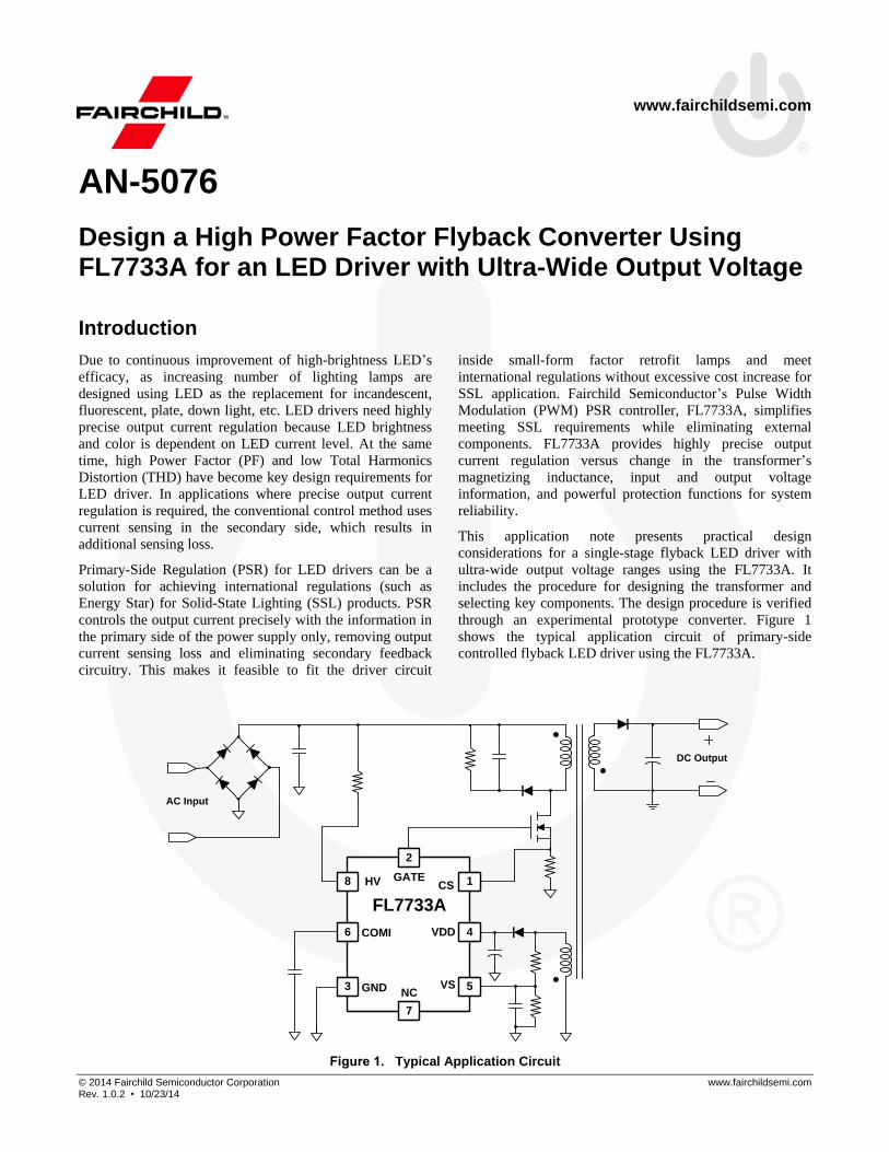
through an experimental prototype converter. Figure 1
shows the typical application circuit of primary-side
controlled flyback LED driver using the FL7733A.
AC Input
COMI
GND VS
HV CSGATE
VDD
DC Output
5
1
2
46
3
8
7
NC
FL7733A
Figure 1. Typical Application Circuit
AN-5076 APPLICATION NOTE
© 2014 Fairchild Semiconductor Corporation www.fairchildsemi.com Rev. 1.0.2 • 10/23/14 2
Operation Principle of Primary-Side Regulation
Generally, Discontinuous Conduction Mode (DCM)
operation is preferred for single-stage primary-side flyback
converters because it allows better output regulation, higher
PF, and lower THD. The operation principles of DCM
flyback converter are as follows:
Mode I
During the MOSFET turn-on time (tON), input voltage (VIN)
is applied across the transformer’s primary-side inductance
(Lm). Then, drain current (IDS) of the MOSFET increases
linearly from zero to the peak value (IDS.PK), as shown in
Figure 3. During this time, the energy is drawn from the
input and stored in the inductor.
Mode II
When the MOSFET (Q) is turned off, the energy stored in
the transformer forces the rectifier diode (D) to turn on.
AC Input
Primary Side Regulation
Controller
tDIS Detector
PWM
Control
Ref EAI
VCS Detector
TRUECURRENT®
Calculation
VCOMI
RS
NP : NSID
IDSQ
D
VCS
VDD
VS
Gate
VA
NA
LM
VIN
VF
+
+ +
Figure 2. Primary-Side Regulated Flyback Converter
While the diode is conducting, output voltage (VOUT) and the
diode forward-voltage drop (VF), is applied across the
transformer’s secondary-side inductance and diode current (ID)
decreases linearly from the peak value (IDS.PK NP/NS) to zero.
At the end of inductor current discharge time (tDIS), all energy
stored in the transformer has been delivered to the output.
Mode III
When the diode current reaches zero, the transformer
auxiliary winding voltage begins to oscillate by the
resonance between the primary-side inductance (Lm) and the
effective capacitor loaded across MOSFET (Q).
VIN
MODE I MODE II MODE III
IO
IDS
ID
VDS
VGate
tDIS
tS
VAOUT
S
A VN
N
IDS.PK
)VV(N
NFOUT
S
P
PK.DS
S
P IN
N
Figure 3. Key Waveforms of PSR Flyback Converter
The output current can be estimated using the peak drain
current and inductor current discharge time because output
current is the same as the average of the diode current in
steady state. The peak value of the drain current is
determined by the CS peak voltage detector and the inductor
current discharge time (tDIS) is sensed by the tDIS detector.
With peak drain current, inductor current discharging time,
and operating switching period information; the innovative
TRUECURRENT® calculation block estimates output
current as follows:
SS
PCS
S
DIS
oRN
NV
t
tI
1
2
1 (1)
25.0 CS
S
DIS Vt
t (2)
SS
Po
RN
NI
1125.0 (3)
AN-5076 APPLICATION NOTE
© 2014 Fairchild Semiconductor Corporation www.fairchildsemi.com Rev. 1.0.2 • 10/23/14 3
Design Procedure
A design procedure for a single-stage flyback LED driver,
based on FL7733A, is presented in this section using the
schematic of Figure 1 as the reference. An offline LED
driver with 50 W (50 V / 1 A) output has been selected as a
design example. The design specifications are:
Input voltage range: 90 ~ 264 VAC and 50 ~ 60 Hz
Nominal output voltage and current: 50 V / 1.0 A
Operating output voltage: 7 V ~ 55 V
Minimum efficiency: 88%
Operating switching frequency: 65 kHz
Maximum duty: 40%
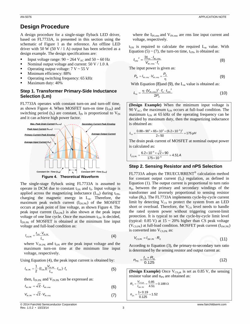
Step 1. Transformer Primary-Side Inductance Selection (Lm)
FL7733A operates with constant turn-on and turn-off time,
as shown Figure 4. When MOSFET turn-on time (tON) and
switching period (tS) are constant, IIN is proportional to VIN
and it can achieve high power factor.
Constant On -Time (tON)
Average Input Current (IIN)
Secondary Current Peak Envelop
Constant OFF -Time (tOFF)
Primary Current Peak Envelop
Max. Peak Drain Current (IDS.PK)
Peak Input Current (IIN.PK)
Average Output Current
tS Figure 4. Theoretical Waveform
The single-stage flyback using FL7733A is assumed to
operate in DCM due to constant tON and tS. Input voltage is
applied across the magnetizing inductance (Lm) during tON,
charging the magnetic energy in Lm. Therefore, the
maximum peak switch current (IDS.PK) of the MOSFET
occurs at peak point of line voltage, as shown Figure 4. The
peak input current (IIN.PK) is also shown at the peak input
voltage of one line cycle. Once the maximum tON is decided,
IDS.PK of MOSFET is obtained at the minimum line input
voltage and full-load condition as:
m
PKINON
PKDSL
VtI .
.
(4)
where VIN.PK and tON are the peak input voltage and the
maximum turn-on time at the minimum line input
voltage, respectively.
Using Equation (4), the peak input current is obtained by:
SON
m
PKINONPKIN ft
L
VtI ))((
2
1 ..
(5)
then, IIN.PK and VIN.PK can be expressed as:
rmsINPKIN II .. 2 (6)
rmsINPKIN VV .. 2 (7)
where the IIN.rms and VIN.rms are rms line input current and
voltage, respectively.
tON is required to calculate the required Lm value. With
Equation (5) ~ (7), the turn-on time, tON, is obtained as:
srmsIN
rmsINmON
fV
ILt
.
.2 2
(8)
The input power is given as:
O
rmsINrmsININ
PVIP ..
(9)
With Equation (8)and (9), the Lm value is obtained as:
O
ONSrmsINm
P
tfVL
2
)(22
.
(10)
(Design Example) When the minimum input voltage is
90 VAC, the maximum tON occurs at full-load condition. The
maximum tON at 65 kHz of the operating frequency can be
decided by maximum duty, then the magnetizing inductance
is obtained as:
HLm µ175502
)102.6(10659088.0 2632
The drain peak current of MOSFET at nominal output power
is calculated as:
AI PKDS 51.410175
902102.66
6
.
Step 2. Sensing Resistor and nPS Selection
FL7733A adopts the TRUECURRENT® calculation method
for constant output current (IO) regulation, as defined in
Equation (1). The output current is proportional to turn ratio
nps between the primary and secondary windings of the
transformer and inversely proportional to sensing resistor
value (RS). The FL7733A implements cycle-by-cycle current
limit by detecting VCS to protect the system from an LED
short or overload. Therefore, the VCS level needs to handle
the rated system power without triggering current-limit
protection. It is typical to set the cycle-by-cycle limit level
(typical: 0.85 V) at 15 ~ 20% higher than CS peak voltage
(VCS.PK) at full-load condition. MOSFET peak current (ISW.PK)
is converted into VCS,PK as:
SPKSWPKCS RIV .. (11)
According to Equation (3), the primary-to-secondary turn ratio
is determined by the sensing resistor and output current as:
125.0
SOPS
RIn
(12)
(Design Example) Once VCS,pk is set as 0.85 V, the sensing
resistor value and nPS are obtained as:
188.051.4
85.0
.
.
PKSW
pkCS
SI
VR
52.1125.0
19.01
psn
AN-5076 APPLICATION NOTE
© 2014 Fairchild Semiconductor Corporation www.fairchildsemi.com Rev. 1.0.2 • 10/23/14 4
Step 3. nAS and nAP Selection
When VDD voltage is 23 V, the FL7733A stops its switching
operation due to Over-Voltage Protection (OVP). So, nAS
and nAP can be determined as follows:
OVPOOVPO
OVPDDAS
VV
Vn
..
. 23 (13)
PS
AS
APn
nn (14)
where, nAS is the auxiliary-to-secondary turns ratio and
nAP is the auxiliary to primary turns ratio of transformer.
(Design Example) Once output over-voltage level is set as
56 V, nAS is obtained as:
41.056
23ASn
27.052.1
41.0APn
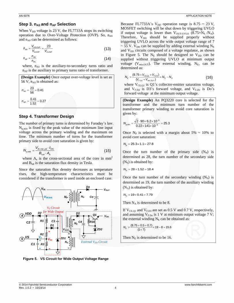
Step 4. Transformer Design
The number of primary turns is determined by Faraday’s law.
Np,min is fixed by the peak value of the minimum line input
voltage across the primary winding and the maximum on
time. The minimum number of turns for the transformer
primary side to avoid core saturation is given by:
esat
ONpkIN
pAB
tVN
.min.
min, (15)
where Ae is the cross-sectional area of the core in mm2
and Bsat is the saturation flux density in Tesla.
Since the saturation flux density decreases as temperature
rises, the high-temperature characteristics must be
considered if the transformer is used inside an enclosed case.
5VS
VOUT
VDD
R1
R2
R3C1
ZD1
D1
C3
NA
NSNP
NE
ZD2
VDD
External VDD Circuit
VS Circuit
for Wide Output
4
VSC
VS
VAUX
++
+
R16C4
D3Q1
VIN.bnk
VINDo
D2
Co
C2
Figure 5. VS Circuit for Wide Output Voltage Range
Because FL7733A’s VDD operation range is 8.75 ~ 23 V,
MOSFET switching will be shut down by triggering UVLO
if output voltage is lower than VOUT-UVLO (8.75×NS /NA).
Therefore, VDD should be supplied properly without
triggering UVLO across the wide output voltage range of 7
~ 55 V. VDD can be supplied by adding external winding NE
and VDD circuits composed of a voltage regulator, as shown
in Figure 5. The NE should be designed so VDD can be
supplied without triggering UVLO at minimum output
voltage (Vmin.OUT). The external winding, NE, can be
determined as:
AS
OUTDoF
F.DQCE
E NNVV
VVN
)(
)75.8(
.min.
31. (16)
where VCE.Q1 is Q1’s collector-emitter saturation voltage,
and VF.D3 is D3’s forward voltage, and VF.Do is Do’s
forward voltage at the minimum output voltage.
(Design Example) An PQ3220 core is selected for the
transformer and the minimum turn number of the
transformer primary winding to avoid core saturation is
given by:
3.251014122.0
102.69026
6
min,
pN
Once NP is selected with a margin about 5% ~ 10% to
avoid core saturation:
8.271.13.25 pN
Once the turn number of the primary side (NP) is
determined as 28, the turn number of the secondary side
(NS) is obtained by:
4.1852.128 SN
Once the turn number of the secondary winding (NS) is
determined as 19, the turn number of the auxiliary winding
(NA) is obtained by:
79.741.019 AN
Then NA is determined to be 8.
If VCE.Q1 and VF.D3 are set as 0.5 V and 0.7 V, respectively,
and assuming VF.Do is 1 V at minimum output voltage 7 V;
the external winding NE can be obtained as:
6.15819)71(
)7.05.075.8(
EN
Then NE is determined to be 16.
AN-5076 APPLICATION NOTE
© 2014 Fairchild Semiconductor Corporation www.fairchildsemi.com Rev. 1.0.2 • 10/23/14 5
Step 5. VS Circuits for Wide Output Range
The first consideration for R1, R2, and R3 selection is that
VS should be 2.45 V at the end of diode current conduction
time to operate at 65 kHz switching frequency at the rated
power. The second consideration is VS blanking, as
explained below. The output voltage is detected by the
auxiliary winding and a resistive divider connected to the
VS pin, as shown in Figure 5. However, in a single-stage
flyback converter without a DC link capacitor, auxiliary
winding voltage cannot be clamped to reflected output
voltage over the whole input line cycle due to the small Lm
current, which induces VS voltage sensing error, as shown in
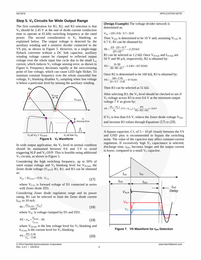
Figure 6. Frequency decreases rapidly at the zero-crossing
point of line voltage, which can cause LED light flicker. To
maintain constant frequency over the whole sinusoidal line
voltage, VS blanking disables VS sampling when line voltage
is below a particular level by sensing the auxiliary winding.
VIN
VIN.BNK
VS.BNK
VS at VIN > VIN.BNK VS at low VIN
VS
Sensing Error
Figure 6. VS Waveform
In wide output application, the VS level in normal condition
should be maintained between 0.6 and 3 V to avoid
triggering SLP and VS OVP. This is feasible using additional
VS circuits, as shown in Figure 5.
Considering the high switching frequency, up to 50% of
rated output voltage and VS blanking level for VIN.bnk, the
Zener diode voltage (VZD1), R1, R2, and R3 can be obtained
as:
1..1 )5.0( DFOVPDDZD VVV (17)
where VF.D1 is forward voltage of D1 connected in series
with Zener diode ZD1.
Considering Zener diode regulation range and its power
rating, R1 can be selected to limit the Zener diode current
IZD1 to 10 mA:
mA10
)VV(1R SCOVPDD
(18)
where VSC is voltage clamped by D1 and ZD1.
12.
. RI
VnR
bnkVS
bnkIN
AP (19)
where VIN.bnk is the line voltage level for VS blanking and
IVS.bnk is the current level for VS blanking.
45.2
45.223
SCV
RR (20)
(Design Example) The voltage divider network is
determined as:
8.107.0)5.023(1 ZDV
Then VZD1 is determined to be 10 V and, assuming VF.D1 is
0.7 V, R1 can be obtained by:
k23.11010
7.010231R
3
R1 can be selected as 1.2 kΩ. Once VIN.bnk and IVS.bnk are
50 V and 90 µA, respectively, R2 is obtained by:
kkR 53.1572.1
109028
5082
6
Once R2 is determined to be 160 kΩ, R3 is obtained by:
kR 51.47
45.27.010
45.21603
Then R3 can be selected as 51 kΩ.
After selecting R3, the VS level should be checked to see if
VS voltage across R3 is over 0.6 V at the minimum output
voltage 7 V as given by:
VRRR
RVV
N
NNVS DoF
S
EA 6.0)321
3()7(
)(.
If VS is less than 0.6 V, reduce the Zener diode voltage VZD1
and increase R3 values through Equations (17) to (20).
A bypass capacitor, C1, of 5 ~ 10 pF closely between the VS
and GND pins is recommended to bypass the switching
noise. The value of the capacitor may affect constant-current
regulation. If excessively high VS capacitance is selected,
discharge time, tDIS, becomes longer and the output current
is lower, compared to a small VS capacitor.
tDIS
IDS IDo
tON
tDIS
Delay
VSC
VS
VAUX
Figure 7. VS Waveform for tDIS Detection
AN-5076 APPLICATION NOTE
© 2014 Fairchild Semiconductor Corporation www.fairchildsemi.com Rev. 1.0.2 • 10/23/14 6
An additional consideration in VS circuits for wide output
voltage range is tDIS delay caused by the voltage difference
between VAUX and VSC when VAUX across auxiliary winding
is clamped to VSC as shown in Figure 7. This delay lasts
until VAUX is the same as VSC and may affect constant output
current regulation. It can be removed by putting a capacitor,
C9, between the auxiliary winding and the cathode of Zener
diode, ZD1. The VAUX is divided with capacitor voltage VC3
and VZD1 when the gate is turned off. Then VC3 is maintained
to its voltage without discharging at the moment, but VZD2 is
decreased to VAUX – VC3 when the diode current ID reaches
zero. Therefore, VS can follow VAUX as the dotted line
shown in Figure 7. C3 should be selected to the proper value
depending on resonant frequency determined by the
resonance between magnetizing inductance Lm and
MOSFET COSS. The 330 pF used in this application was
selected by trial and error. Its value can be obtained as:
pFf
kHzC
r
330300
3
(21)
where fr is the resonance frequency determined by the
resonance between COSS and Lm.
Step 6. Calculate the Voltage and Current of the Switching Devices
Primary-Side MOSFET: The voltage stress of the
MOSFET is discussed in determining the transformer turns
ratio. Assuming the drain voltage overshoot is considered as
certain voltage VOS, the maximum drain voltage is given as:
OSDoFOVPO
S
PpkINDS VVV
N
NVV )( ...max.(max) (22)
where VIN.max.pk is the maximum line peak voltage and VOS
is the drain voltage overshoot. The rms current (ISW.rms)
though the MOSFET is given as:
6.
SON
pkrmsDS
ftII
(23)
(Design Example) Assuming that drain voltage overshoot is
about 100 V, the maximum drain voltage across the MOSFET
is calculated as:
VVDS 559100)156(19
282265(max)
The rms current though the MOSFET is:
AI rmsDS 17.16
1065102.651.4
36
.
Secondary-Side Diode: The maximum reverse voltage and
rms current of the rectifier diode are obtained as:
pkin
P
SOD V
N
NVV .max.
(24)
S
P
RO
pkin
rmsSWrmsDN
N
V
VII
2
.min.
..
(25)
(Design Example) Diode voltage and current are obtained as:
VVD 310226528
1956
AI rmsD 991.020
60
1.742
127357.0.
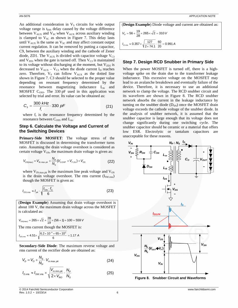
Step 7. Design RCD Snubber in Primary Side
When the power MOSFET is turned off, there is a high-
voltage spike on the drain due to the transformer leakage
inductance. This excessive voltage on the MOSFET may
lead to an avalanche breakdown and eventually failure of the
device. Therefore, it is necessary to use an additional
network to clamp the voltage. The RCD snubber circuit and
its waveform are shown in Figure 8. The RCD snubber
network absorbs the current in the leakage inductance by
turning on the snubber diode (DSN) once the MOSFET drain
voltage exceeds the cathode voltage of the snubber diode. In
the analysis of snubber network, it is assumed that the
snubber capacitor is large enough that its voltage does not
change significantly during one switching cycle. The
snubber capacitor should be ceramic or a material that offers
low ESR. Electrolytic or tantalum capacitors are
unacceptable for these reasons.
Lm
RSN
DSN
CSN
CO
Llk
VOUT
VSN
NP : NSVIN
IDS
VDS
+
+
+
VSN
VDS
VOS
)( FOUT
S
P VVN
N
VIN
ID
IDS.PK
ID
Figure 8. Snubber Circuit and Waveforms
AN-5076 APPLICATION NOTE
© 2014 Fairchild Semiconductor Corporation www.fairchildsemi.com Rev. 1.0.2 • 10/23/14 7
Snubber capacitor voltage at full-load condition is given as:
OSROSN VVV (26)
The power dissipated in the snubber network is obtained as:
S
ROSN
SN
PKDSlk
SN
SN
SN fVV
VIL
R
VP
2
..
2
2
1 (27)
where Llk is leakage inductance, VSN is snubber capacitor
voltage at full load, and RSN is the snubber resistor.
The leakage inductance is measured at the switching
frequency on the primary winding with all other windings
shorted. The snubber resistor with proper rated wattage
should be chosen based on the power loss. The maximum
ripple of the snubber capacitor voltage is obtained as:
SSNSN
SNSN
fRC
VV
(28)
In general, 5 ~ 20% ripple of the selected capacitor voltage
is reasonable. In this snubber design, neither the lossy
discharge of the inductor nor stray capacitance is considered.
(Design Example) Since the voltage overshoot of the drain
voltage has been determined to be the same as the reflected
output voltage, the snubber voltage is:
VVVV OSROSN 200
The leakage inductance is measured as 3 µH. Then the loss
in snubber networking is given as:
W
PSN
48.3
106584200
20056.4105
2
1 326
kRSN 45.1148.3
2002
To allow 15% ripple on the snubber voltage (200 V):
nFCSN 9.81065101220015.0
20033
AN-5076 APPLICATION NOTE
© 2014 Fairchild Semiconductor Corporation www.fairchildsemi.com Rev. 1.0.2 • 10/23/14 8
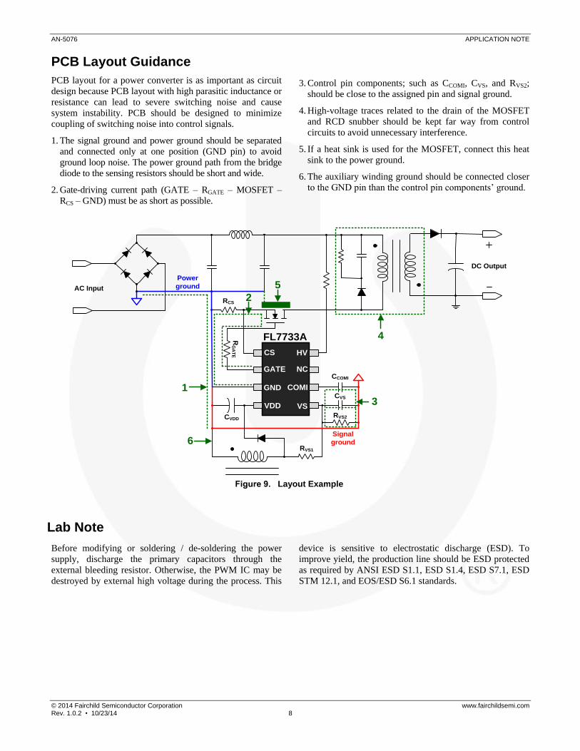
PCB Layout Guidance
PCB layout for a power converter is as important as circuit
design because PCB layout with high parasitic inductance or
resistance can lead to severe switching noise and cause
system instability. PCB should be designed to minimize
coupling of switching noise into control signals.
1. The signal ground and power ground should be separated
and connected only at one position (GND pin) to avoid
ground loop noise. The power ground path from the bridge
diode to the sensing resistors should be short and wide.
2. Gate-driving current path (GATE – RGATE – MOSFET –
RCS – GND) must be as short as possible.
3. Control pin components; such as CCOMI, CVS, and RVS2;
should be close to the assigned pin and signal ground.
4. High-voltage traces related to the drain of the MOSFET
and RCD snubber should be kept far way from control
circuits to avoid unnecessary interference.
5. If a heat sink is used for the MOSFET, connect this heat
sink to the power ground.
6. The auxiliary winding ground should be connected closer
to the GND pin than the control pin components’ ground.
FL7733A
AC Input
GND
GATE
VDD VS
CS
COMI
NC
HV
DC Output
RCS
RG
AT
E
CVDD
CCOMI
CVS
RVS2
RVS1
1
2
3
4
5Power
ground
Signal
ground6
Figure 9. Layout Example
Lab Note
Before modifying or soldering / de-soldering the power
supply, discharge the primary capacitors through the
external bleeding resistor. Otherwise, the PWM IC may be
destroyed by external high voltage during the process. This
device is sensitive to electrostatic discharge (ESD). To
improve yield, the production line should be ESD protected
as required by ANSI ESD S1.1, ESD S1.4, ESD S7.1, ESD
STM 12.1, and EOS/ESD S6.1 standards.
AN-5076 APPLICATION NOTE
© 2014 Fairchild Semiconductor Corporation www.fairchildsemi.com Rev. 1.0.2 • 10/23/14 9
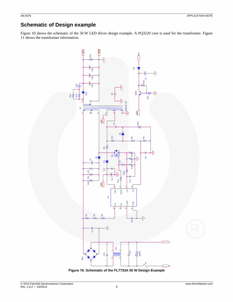
Schematic of Design example
Figure 10 shows the schematic of the 50 W LED driver design example. A PQ3220 core is used for the transformer. Figure
11 shows the transformer information.
Figure 10. Schematic of the FL7733A 50 W Design Example
VD
D
C8
R5
C1
0
U1
CO
MI
6
GA
TE
2
CS
1
VD
D4
HV
8
NC
7
GN
D3
VS
5
VD
D
C3
R1
7
C4
D2
Aux
R8
ZD
2
R9
R1
T2
PQ
32
20
12
V
61 2 4
9 11
53
R2
R3
D5
Aux
C6
R1
3
R1
0R
11
BD
1
Q1
R1
4
R1
2
C2 C
5
R4
C9
C1
Co
2
50V
GN
D
Co
3
D1
R7
R1
8
C7
CF
2
Q103
R1
6
ZD
1
D3
R2
0
R1
9
CF
1
F1
NL
Do
1
LF
1
34
21
Ro
1C
o1
MO
V1
C1
1
R6
AN-5076 APPLICATION NOTE
© 2014 Fairchild Semiconductor Corporation www.fairchildsemi.com Rev. 1.0.2 • 10/23/14 10
NP1(3 à2)
NS (9 à11)
NA(4 à5)
NP2(2 à1)
Start
NE(6 à4)
2mm Barrier
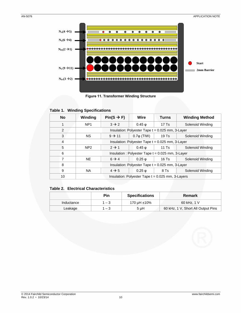
Figure 11. Transformer Winding Structure
Table 1. Winding Specifications
No Winding Pin(S à F) Wire Turns Winding Method
1 NP1 3 à 2 0.45 φ 17 Ts Solenoid Winding
2 Insulation: Polyester Tape t = 0.025 mm, 3-Layer
3 NS 9 à 11 0.7φ (TIW) 19 Ts Solenoid Winding
4 Insulation: Polyester Tape t = 0.025 mm, 3-Layer
5 NP2 2 à 1 0.45 φ 11 Ts Solenoid Winding
6 Insulation : Polyester Tape t = 0.025 mm, 3-Layer
7 NE 6 à 4 0.25 φ 16 Ts Solenoid Winding
8 Insulation: Polyester Tape t = 0.025 mm, 3-Layer
9 NA 4 à 5 0.25 φ 8 Ts Solenoid Winding
10 Insulation: Polyester Tape t = 0.025 mm, 3-Layers
Table 2. Electrical Characteristics
Pin Specifications Remark
Inductance 1 – 3 170 µH ±10% 60 kHz, 1 V
Leakage 1 – 3 5 µH 60 kHz, 1 V, Short All Output Pins
AN-5076 APPLICATION NOTE
© 2014 Fairchild Semiconductor Corporation www.fairchildsemi.com Rev. 1.0.2 • 10/23/14 11
Bill of Materials
Item
No.
Part
Reference Part Number Qty. Description Manufacturer
1 BD1 G3SBA60 1 4 A / 600 V, Bridge Diode Vishay
2 CF1 MPX AC275V 474K 1 470 nF / 275 VAC, X-Capacitor Carli
3 CF2 MPX AC275V 224K 1 220 nF / 275 VAC, X-Capacitor Carli
4 Co1, Co2, Co3 KMG 470 μF / 63 V 3 470 µF / 63 V, Electrolytic Capacitor Samyoung
5 C1 MPE 630 V 334K 1 330 nF / 630 V, MPE Film Capacitor Sungho
6 C2 C1206C103KDRACTU 1 10 nF / 630 V, SMD Capacitor 1206 Kemet
7 C3 KMG 10 μF / 35 V 1 10 µF / 35 V, Electrolytic Capacitor Samyoung
8 C4 C0805C104K5RACTU 1 100 nF / 50 V, SMD Capacitor 2012 Kemet
9 C5 C0805C519C3GACTU 1 5.1 pF / 25 V, SMD Capacitor 2012 Kemet
10 C6 C0805C205J3RACTU 1 2.2 µF / 25 V, SMD Capacitor 2012 Kemet
11 C7 KMG 1 μF / 50 V 1 1 µF / 50 V, Electrolytic Capacitor Samyoung
12 C8 SCFz2E472M10BW 1 4.7 nF / 250 V, Y-Capacitor Samwha
13 C9 C1206C331K5RACTU 1 330 pF / 630 V, SMD Capacitor 1206 Kemet
14 C10 C1206C471KDRACTU 1 470 pF / 630 V, SMD Capacitor 1206 Kemet
15 C11 C0805C101C3GACTU 1 100 pF / 25 V, SMD Capacitor 0805 Kemet
16 Do1 FFPF08H60S 1 600 V / 8 A, Hyper-Fast Rectifier Fairchild Semiconductor
17 D1, D3 RS1M 2 1000 V / 1 A, Ultra-Fast Recovery Diode Fairchild Semiconductor
18 D2 1N4003 1 200 V / 1 A, General-Purpose Rectifier Fairchild Semiconductor
19 D5 LL4148 1 100 V / 0.2 A, Small Signal Diode Fairchild Semiconductor
20 F1 250 V / 2 A 1 250 V / 2 A, Fuse Bussmann
21 LF1 B82733F 1 40 mH Common Inductor EPCOS
22 MOV1 SVC681D-10A 1 Metal Oxide Varistor Samwha
23 Q1 FCPF400N80Z 1 800 V / 400 mΩ, N-Channel MOSFET Fairchild Semiconductor
24 Q103 KSP42 1 High-Voltage NPN Transistor Fairchild Semiconductor
25 Ro1 RC1206JR-0727KL 1 27 kΩ, SMD Resistor 1206 Yageo
26 R1, R7 RC1206JR-0710KL 2 10 kΩ, SMD Resistor 1206 Yageo
27 R2, R3 RC1206JR-0715KL 2 15 kΩ, SMD Resistor 1206 Yageo
28 R4, R5, R20 RC1206JR-07100KL 3 100 kΩ, SMD Resistor 1206 Yageo
29 R6, R15 RC1206JR-0710RL 2 10 Ω, SMD Resistor 1206 Yageo
30 R8 RC0805JR-07160KL 1 160 kΩ, SMD Resistor 0805 Yageo
31 R9 RC0805JR-0727KL 1 56 kΩ, SMD Resistor 0805 Yageo
32 R10 RC1206JR-070R2L 1 0.2 Ω, SMD Resistor 1206 Yageo
33 R11, R12 RC1206JR-073RL 2 3.0 Ω, SMD Resistor 1206 Yageo
34 R13 RC0805JR-0710RL 1 10 Ω, SMD Resistor 0805 Yageo
35 R14 RC0805JR-07510RL 1 510 Ω, SMD Resistor 0805 Yageo
36 R16 RC1206JR-0730kL 1 30 kΩ, SMD Resistor 1206 Yageo
37 R17 RC1206JR-071KL 1 1.0 kΩ, SMD Resistor 1206 Yageo
38 R18, R19 RC1206JR-07300RL 2 300 Ω, SMD Resistor 1206 Yageo
39 T2 PQ3220 1 PQ Core, 12Pin Transformer TDK
40 U1 FL7733A 1 Main PSR Controller Fairchild Semiconductor
41 ZD1 15 V 1 15 V Zener Diode Fairchild Semiconductor
42 ZD2 10 V 1 10 V Zener Diode Fairchild Semiconductor
AN-5076 APPLICATION NOTE
© 2014 Fairchild Semiconductor Corporation www.fairchildsemi.com Rev. 1.0.2 • 10/23/14 12
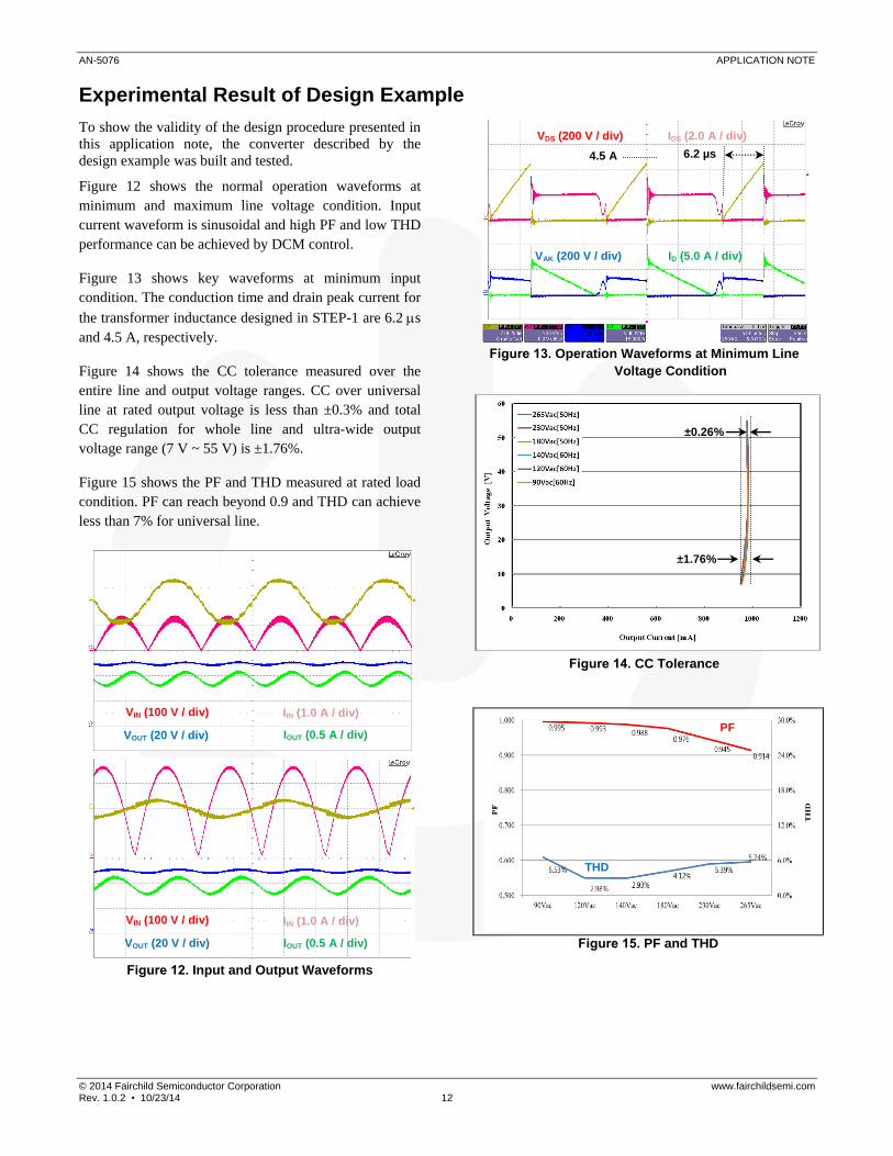
Experimental Result of Design Example
To show the validity of the design procedure presented in
this application note, the converter described by the
design example was built and tested.
Figure 12 shows the normal operation waveforms at
minimum and maximum line voltage condition. Input
current waveform is sinusoidal and high PF and low THD
performance can be achieved by DCM control.
Figure 13 shows key waveforms at minimum input
condition. The conduction time and drain peak current for
the transformer inductance designed in STEP-1 are 6.2 s
and 4.5 A, respectively.
Figure 14 shows the CC tolerance measured over the
entire line and output voltage ranges. CC over universal
line at rated output voltage is less than ±0.3% and total
CC regulation for whole line and ultra-wide output
voltage range (7 V ~ 55 V) is ±1.76%.
Figure 15 shows the PF and THD measured at rated load
condition. PF can reach beyond 0.9 and THD can achieve
less than 7% for universal line.
Figure 12. Input and Output Waveforms
Figure 13. Operation Waveforms at Minimum Line
Voltage Condition
Figure 14. CC Tolerance
Figure 15. PF and THD
VIN (100 V / div) IIN (1.0 A / div)
VOUT (20 V / div) IOUT (0.5 A / div)
4.5 A
VDS (200 V / div) IDS (2.0 A / div)
VAK (200 V / div) ID (5.0 A / div)
6.2 µs
±0.26%
±1.76%
VIN (100 V / div)
VOUT (20 V / div)
IIN (1.0 A / div)
IOUT (0.5 A / div) PF
THD
AN-5076 APPLICATION NOTE
© 2014 Fairchild Semiconductor Corporation www.fairchildsemi.com Rev. 1.0.2 • 10/23/14 13
Related Product Resources
FL7733A — Primary-Side-Regulated LED Driver with Power Factor Correction
DISCLAIMER
FAIRCHILD SEMICONDUCTOR RESERVES THE RIGHT TO MAKE CHANGES WITHOUT FURTHER NOTICE TO ANY PRODUCTS HEREIN TO IMPROVE RELIABILITY, FUNCTION, OR DESIGN. FAIRCHILD DOES NOT ASSUME ANY LIABILITY ARISING OUT OF THE APPLICATION OR USE OF ANY PRODUCT OR CIRCUIT DESCRIBED HEREIN; NEITHER DOES IT CONVEY ANY LICENSE UNDER ITS PATENT RIGHTS, NOR THE RIGHTS OF OTHERS. LIFE SUPPORT POLICY FAIRCHILD’S PRODUCTS ARE NOT AUTHORIZED FOR USE AS CRITICAL COMPONENTS IN LIFE SUPPORT DEVICES OR SYSTEMS WITHOUT THE EXPRESS WRITTEN APPROVAL OF THE PRESIDENT OF FAIRCHILD SEMICONDUCTOR CORPORATION. As used herein:
1. Life support devices or systems are devices or systems which, (a) are intended for surgical implant into the body, or (b) support or sustain life, or (c) whose failure to perform when properly used in accordance with instructions for use provided in the labeling, can be reasonably expected to result in significant injury to the user.
2. A critical component is any component of a life support device or system whose failure to perform can be reasonably expected to cause the failure of the life support device or system, or to affect its safety or effectiveness.
www.onsemi.com1
ON Semiconductor and are trademarks of Semiconductor Components Industries, LLC dba ON Semiconductor or its subsidiaries in the United States and/or other countries.ON Semiconductor owns the rights to a number of patents, trademarks, copyrights, trade secrets, and other intellectual property. A listing of ON Semiconductor’s product/patentcoverage may be accessed at www.onsemi.com/site/pdf/Patent−Marking.pdf. ON Semiconductor reserves the right to make changes without further notice to any products herein.ON Semiconductor makes no warranty, representation or guarantee regarding the suitability of its products for any particular purpose, nor does ON Semiconductor assume any liabilityarising out of the application or use of any product or circuit, and specifically disclaims any and all liability, including without limitation special, consequential or incidental damages.Buyer is responsible for its products and applications using ON Semiconductor products, including compliance with all laws, regulations and safety requirements or standards,regardless of any support or applications information provided by ON Semiconductor. “Typical” parameters which may be provided in ON Semiconductor data sheets and/orspecifications can and do vary in different applications and actual performance may vary over time. All operating parameters, including “Typicals” must be validated for each customerapplication by customer’s technical experts. ON Semiconductor does not convey any license under its patent rights nor the rights of others. ON Semiconductor products are notdesigned, intended, or authorized for use as a critical component in life support systems or any FDA Class 3 medical devices or medical devices with a same or similar classificationin a foreign jurisdiction or any devices intended for implantation in the human body. Should Buyer purchase or use ON Semiconductor products for any such unintended or unauthorizedapplication, Buyer shall indemnify and hold ON Semiconductor and its officers, employees, subsidiaries, affiliates, and distributors harmless against all claims, costs, damages, andexpenses, and reasonable attorney fees arising out of, directly or indirectly, any claim of personal injury or death associated with such unintended or unauthorized use, even if suchclaim alleges that ON Semiconductor was negligent regarding the design or manufacture of the part. ON Semiconductor is an Equal Opportunity/Affirmative Action Employer. Thisliterature is subject to all applicable copyright laws and is not for resale in any manner.
PUBLICATION ORDERING INFORMATIONN. American Technical Support: 800−282−9855 Toll FreeUSA/Canada
Europe, Middle East and Africa Technical Support:Phone: 421 33 790 2910
Japan Customer Focus CenterPhone: 81−3−5817−1050
www.onsemi.com
LITERATURE FULFILLMENT:Literature Distribution Center for ON Semiconductor19521 E. 32nd Pkwy, Aurora, Colorado 80011 USAPhone: 303−675−2175 or 800−344−3860 Toll Free USA/CanadaFax: 303−675−2176 or 800−344−3867 Toll Free USA/CanadaEmail: [email protected]
ON Semiconductor Website: www.onsemi.com
Order Literature: http://www.onsemi.com/orderlit
For additional information, please contact your localSales Representative
© Semiconductor Components Industries, LLC